KR100858818B1 - Thin film transistor and flat panel display device having same - Google Patents
Thin film transistor and flat panel display device having sameDownload PDFInfo
- Publication number
- KR100858818B1 KR100858818B1KR1020070027246AKR20070027246AKR100858818B1KR 100858818 B1KR100858818 B1KR 100858818B1KR 1020070027246 AKR1020070027246 AKR 1020070027246AKR 20070027246 AKR20070027246 AKR 20070027246AKR 100858818 B1KR100858818 B1KR 100858818B1
- Authority
- KR
- South Korea
- Prior art keywords
- layer
- electrode
- thin film
- film transistor
- source
- Prior art date
- Legal status (The legal status is an assumption and is not a legal conclusion. Google has not performed a legal analysis and makes no representation as to the accuracy of the status listed.)
- Active
Links
- 239000010409thin filmSubstances0.000titleclaimsabstractdescription51
- 239000004065semiconductorSubstances0.000claimsabstractdescription20
- 239000010936titaniumSubstances0.000claimsabstractdescription20
- 229910052782aluminiumInorganic materials0.000claimsabstractdescription13
- 229910052750molybdenumInorganic materials0.000claimsabstractdescription8
- ZOKXTWBITQBERF-UHFFFAOYSA-NMolybdenumChemical compound[Mo]ZOKXTWBITQBERF-UHFFFAOYSA-N0.000claimsabstractdescription7
- RTAQQCXQSZGOHL-UHFFFAOYSA-NTitaniumChemical compound[Ti]RTAQQCXQSZGOHL-UHFFFAOYSA-N0.000claimsabstractdescription7
- XAGFODPZIPBFFR-UHFFFAOYSA-NaluminiumChemical compound[Al]XAGFODPZIPBFFR-UHFFFAOYSA-N0.000claimsabstractdescription7
- 239000011733molybdenumSubstances0.000claimsabstractdescription7
- 229910052719titaniumInorganic materials0.000claimsabstractdescription7
- 238000000034methodMethods0.000claimsdescription25
- 239000000758substrateSubstances0.000claimsdescription14
- 238000007254oxidation reactionMethods0.000abstractdescription2
- AMGQUBHHOARCQH-UHFFFAOYSA-Nindium;oxotinChemical compound[In].[Sn]=OAMGQUBHHOARCQH-UHFFFAOYSA-N0.000abstract1
- 230000003647oxidationEffects0.000abstract1
- 239000010410layerSubstances0.000description136
- 239000011368organic materialSubstances0.000description7
- 239000000463materialSubstances0.000description6
- 238000002161passivationMethods0.000description6
- 239000011229interlayerSubstances0.000description5
- 238000005530etchingMethods0.000description4
- 239000010408filmSubstances0.000description4
- PQXKHYXIUOZZFA-UHFFFAOYSA-Mlithium fluorideInorganic materials[Li+].[F-]PQXKHYXIUOZZFA-UHFFFAOYSA-M0.000description4
- 239000012299nitrogen atmosphereSubstances0.000description4
- 229910004298SiO 2Inorganic materials0.000description3
- 150000001875compoundsChemical class0.000description3
- 238000002347injectionMethods0.000description3
- 239000007924injectionSubstances0.000description3
- 238000004519manufacturing processMethods0.000description3
- 229910052709silverInorganic materials0.000description3
- 229910004205SiNXInorganic materials0.000description2
- -1acrylChemical group0.000description2
- UMIVXZPTRXBADB-UHFFFAOYSA-NbenzocyclobuteneChemical compoundC1=CC=C2CCC2=C1UMIVXZPTRXBADB-UHFFFAOYSA-N0.000description2
- NIHNNTQXNPWCJQ-UHFFFAOYSA-NfluoreneChemical compoundC1=CC=C2CC3=CC=CC=C3C2=C1NIHNNTQXNPWCJQ-UHFFFAOYSA-N0.000description2
- 230000005525hole transportEffects0.000description2
- 229910052749magnesiumInorganic materials0.000description2
- 229910052751metalInorganic materials0.000description2
- 239000002184metalSubstances0.000description2
- 238000012986modificationMethods0.000description2
- 230000004048modificationEffects0.000description2
- 238000000623plasma-assisted chemical vapour depositionMethods0.000description2
- 229920000642polymerPolymers0.000description2
- 238000007789sealingMethods0.000description2
- 239000002356single layerSubstances0.000description2
- YOZHUJDVYMRYDM-UHFFFAOYSA-N4-(4-anilinophenyl)-3-naphthalen-1-yl-n-phenylanilineChemical compoundC=1C=C(C=2C(=CC(NC=3C=CC=CC=3)=CC=2)C=2C3=CC=CC=C3C=CC=2)C=CC=1NC1=CC=CC=C1YOZHUJDVYMRYDM-UHFFFAOYSA-N0.000description1
- 229910052779NeodymiumInorganic materials0.000description1
- 229910052581Si3N4Inorganic materials0.000description1
- VYPSYNLAJGMNEJ-UHFFFAOYSA-NSilicium dioxideChemical compoundO=[Si]=OVYPSYNLAJGMNEJ-UHFFFAOYSA-N0.000description1
- 229910021417amorphous siliconInorganic materials0.000description1
- 229910052804chromiumInorganic materials0.000description1
- 229920001940conductive polymerPolymers0.000description1
- 239000010949copperSubstances0.000description1
- XCJYREBRNVKWGJ-UHFFFAOYSA-Ncopper(II) phthalocyanineChemical compound[Cu+2].C12=CC=CC=C2C(N=C2[N-]C(C3=CC=CC=C32)=N2)=NC1=NC([C]1C=CC=CC1=1)=NC=1N=C1[C]3C=CC=CC3=C2[N-]1XCJYREBRNVKWGJ-UHFFFAOYSA-N0.000description1
- 238000000151depositionMethods0.000description1
- 230000008021depositionEffects0.000description1
- 239000002019doping agentSubstances0.000description1
- 239000011521glassSubstances0.000description1
- 229910052737goldInorganic materials0.000description1
- RBTKNAXYKSUFRK-UHFFFAOYSA-Nheliogen blueChemical compound[Cu].[N-]1C2=C(C=CC=C3)C3=C1N=C([N-]1)C3=CC=CC=C3C1=NC([N-]1)=C(C=CC=C3)C3=C1N=C([N-]1)C3=CC=CC=C3C1=N2RBTKNAXYKSUFRK-UHFFFAOYSA-N0.000description1
- 238000007641inkjet printingMethods0.000description1
- 229910010272inorganic materialInorganic materials0.000description1
- 239000011147inorganic materialSubstances0.000description1
- 239000011810insulating materialSubstances0.000description1
- 238000009413insulationMethods0.000description1
- 229910052741iridiumInorganic materials0.000description1
- 239000004973liquid crystal related substanceSubstances0.000description1
- IBHBKWKFFTZAHE-UHFFFAOYSA-Nn-[4-[4-(n-naphthalen-1-ylanilino)phenyl]phenyl]-n-phenylnaphthalen-1-amineChemical compoundC1=CC=CC=C1N(C=1C2=CC=CC=C2C=CC=1)C1=CC=C(C=2C=CC(=CC=2)N(C=2C=CC=CC=2)C=2C3=CC=CC=C3C=CC=2)C=C1IBHBKWKFFTZAHE-UHFFFAOYSA-N0.000description1
- 229910052759nickelInorganic materials0.000description1
- 238000005121nitridingMethods0.000description1
- 229910052757nitrogenInorganic materials0.000description1
- 229910052763palladiumInorganic materials0.000description1
- 230000000704physical effectEffects0.000description1
- 239000004033plasticSubstances0.000description1
- 229910052697platinumInorganic materials0.000description1
- 229910021420polycrystalline siliconInorganic materials0.000description1
- 230000001681protective effectEffects0.000description1
- 239000011241protective layerSubstances0.000description1
- 238000007650screen-printingMethods0.000description1
- 239000003566sealing materialSubstances0.000description1
- HQVNEWCFYHHQES-UHFFFAOYSA-Nsilicon nitrideChemical compoundN12[Si]34N5[Si]62N3[Si]51N64HQVNEWCFYHHQES-UHFFFAOYSA-N0.000description1
- 229910052814silicon oxideInorganic materials0.000description1
- TVIVIEFSHFOWTE-UHFFFAOYSA-Ktri(quinolin-8-yloxy)alumaneChemical compound[Al+3].C1=CN=C2C([O-])=CC=CC2=C1.C1=CN=C2C([O-])=CC=CC2=C1.C1=CN=C2C([O-])=CC=CC2=C1TVIVIEFSHFOWTE-UHFFFAOYSA-K0.000description1
- 238000001771vacuum depositionMethods0.000description1
Images


Classifications
- H—ELECTRICITY
- H10—SEMICONDUCTOR DEVICES; ELECTRIC SOLID-STATE DEVICES NOT OTHERWISE PROVIDED FOR
- H10D—INORGANIC ELECTRIC SEMICONDUCTOR DEVICES
- H10D30/00—Field-effect transistors [FET]
- H10D30/60—Insulated-gate field-effect transistors [IGFET]
- H10D30/67—Thin-film transistors [TFT]
- H10D30/6729—Thin-film transistors [TFT] characterised by the electrodes
- H10D30/6737—Thin-film transistors [TFT] characterised by the electrodes characterised by the electrode materials
- H—ELECTRICITY
- H10—SEMICONDUCTOR DEVICES; ELECTRIC SOLID-STATE DEVICES NOT OTHERWISE PROVIDED FOR
- H10D—INORGANIC ELECTRIC SEMICONDUCTOR DEVICES
- H10D30/00—Field-effect transistors [FET]
- H10D30/60—Insulated-gate field-effect transistors [IGFET]
- H10D30/67—Thin-film transistors [TFT]
- H10D30/674—Thin-film transistors [TFT] characterised by the active materials
- H10D30/6741—Group IV materials, e.g. germanium or silicon carbide
- H10D30/6743—Silicon
- H—ELECTRICITY
- H10—SEMICONDUCTOR DEVICES; ELECTRIC SOLID-STATE DEVICES NOT OTHERWISE PROVIDED FOR
- H10K—ORGANIC ELECTRIC SOLID-STATE DEVICES
- H10K59/00—Integrated devices, or assemblies of multiple devices, comprising at least one organic light-emitting element covered by group H10K50/00
- H10K59/10—OLED displays
- H10K59/12—Active-matrix OLED [AMOLED] displays
- H10K59/131—Interconnections, e.g. wiring lines or terminals
Landscapes
- Engineering & Computer Science (AREA)
- Microelectronics & Electronic Packaging (AREA)
- Electroluminescent Light Sources (AREA)
Abstract
Description
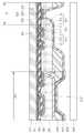
Translated fromKorean도 1은 종래의 유기 발광 디스플레이 장치의 일부를 개략적으로 도시하는 단면도이다.1 is a cross-sectional view schematically illustrating a part of a conventional organic light emitting display device.
도 2는 본 발명의 일 실시예에 따른 박막 트랜지스터를 개략적으로 도시하는 단면도이다.2 is a cross-sectional view schematically illustrating a thin film transistor according to an exemplary embodiment of the present invention.
도 3은 본 발명의 다른 일 실시예에 따른 유기 발광 디스플레이 장치의 일부를 개략적으로 도시하는 단면도이다.3 is a cross-sectional view schematically illustrating a portion of an organic light emitting display device according to another embodiment of the present invention.
<도면의 주요 부분에 대한 부호의 설명><Explanation of symbols for the main parts of the drawings>
100: 디스플레이부 110: 기판100: display unit 110: substrate
120: 버퍼층 130: 반도체층120: buffer layer 130: semiconductor layer
140: 게이트 절연막 150: 게이트 전극140: gate insulating film 150: gate electrode
160: 층간 절연막 170: 소스/드레인 전극160: interlayer insulating film 170: source / drain electrodes
180: 보호막 210: 제1전극180: protective film 210: first electrode
220: 화소 정의막230: 중간층220: pixel defining layer 230: intermediate layer
250: 제2전극300: 배선250: second electrode 300: wiring
400: 봉지기판400: sealing board
본 발명은 박막 트랜지스터 및 이를 구비한 평판 디스플레이 장치에 관한 것으로서, 더 상세하게는 박막 트랜지스터의 전극과 동시에 형성되는 배선의 저항을 감소시키면서도 제조 중 배선이 손상되는 것을 방지하는 박막 트랜지스터 및 이를 구비한 평판 디스플레이 장치에 관한 것이다.BACKGROUND OF THE INVENTION 1. Field of the Invention The present invention relates to a thin film transistor and a flat panel display device having the same, and more particularly, to a thin film transistor and a flat plate having the same to reduce the resistance of the wiring formed at the same time as the electrode of the thin film transistor while preventing the wiring. It relates to a display device.
도 1은 종래의 유기 발광 디스플레이 장치의 일부를 개략적으로 도시하는 단면도이다. 도 1에 도시된 것과 같이 일반적으로 평판 디스플레이 장치는 기판(11) 상에 형성된 디스플레이부(10)와, 디스플레이부(10) 외측의 배선부(A)에 형성된 배선(30)을 구비한다. 유기 발광 디스플레이 장치 등과 같은 평판 디스플레이 장치의 경우 디스플레이부에 화소전극(21), 중간층(23) 및 대향전극(25)을 구비한 복수개의 유기 발광 소자들이 배치되는데, 능동 구동형 유기 발광 디스플레이 장치의 경우에는 각 유기 발광 소자에 구비된 박막 트랜지스터를 통해 각 유기 발광 소자의 발광여부 및 발광정도를 제어한다. 이 경우 제조 공정을 단순화하고 제조비용을 절약하기 위하여 통상적으로 디스플레이부에 배치되는 박막 트랜지스터의 소스 전극 및 드레인 전극 형성 시 디스플레이부 외측에 배치되는 배선의 형성을 동시에 하게 된다.1 is a cross-sectional view schematically illustrating a part of a conventional organic light emitting display device. As shown in FIG. 1, a flat panel display apparatus generally includes a
통상적으로 종래의 박막 트랜지스터의 소스 전극 및 드레인 전극은 Ti층 및 Al층을 포함한 다층으로 형성되거나 Mo층 및 Al층을 포함한 다층으로 형성되었다.In general, the source electrode and the drain electrode of the conventional thin film transistor are formed in a multilayer including a Ti layer and an Al layer, or a multilayer including a Mo layer and an Al layer.
그러나 Ti층이 최상부에 위치할 경우 소스 전극 및 드레인 전극을 형성한 후의 후속 공정이 질소 분위기에서 이루어질 경우 Ti층이 질화되거나, 후속 공정 중 식각 등의 공정을 거칠 경우 Ti층이 산화된다는 문제점이 있었다. 소스 전극 및 드레인 전극의 최상부층인 Ti층의 질화 또는 산화는 이후 소스 전극 및 드레인 전극 중 어느 한 전극에 전기적으로 연결되는 발광 소자 등의 화소 전극(21)과의 소스 전극 및 드레인 전극 사이의 컨택저항이 커져 평판 디스플레이 장치의 품질을 저하시킨다는 문제가 있었다.However, when the Ti layer is located at the top, there is a problem that the Ti layer is nitrided when the subsequent process after forming the source electrode and the drain electrode is performed in a nitrogen atmosphere, or the Ti layer is oxidized when the Ti layer is subjected to an etching process during the subsequent process. . Nitriding or oxidization of the Ti layer, which is the top layer of the source electrode and the drain electrode, is then performed by contact between the source electrode and the drain electrode with the
또한 Mo층이 최상부에 위치할 경우 소스 전극 및 드레인 전극을 형성할 시 동시에 형성하는 배선(30)의 최상부층 역시 Mo층이 되는 바, 이는 배선(30)을 형성한 후 후속 공정에서 화소 전극(21) 등을 형성하면서 거치게 되는 식각 공정 중 쉽게 손상된다는 문제점이 있었다.In addition, when the Mo layer is located at the top, the top layer of the
본 발명은 상기와 같은 문제점을 포함하여 여러 문제점들을 해결하기 위한 것으로서, 박막 트랜지스터의 전극과 동시에 형성되는 배선의 저항을 감소시키면서도 제조 중 배선이 손상되는 것을 방지하는 박막 트랜지스터 및 이를 구비한 평판 디스플레이 장치를 제공하는 것을 목적으로 한다.SUMMARY OF THE INVENTION The present invention has been made to solve a number of problems, including the above problems, a thin film transistor and a flat panel display device having the same to prevent damage to the wiring during manufacturing while reducing the resistance of the wiring formed at the same time as the electrode of the thin film transistor. The purpose is to provide.
본 발명은 복수개의 층상 구조를 가지며 최상부층은 ITO로 형성된 소스 전극 및 드레인 전극과, 상기 소스 전극과 상기 드레인 전극에 각각 접하는 반도체층과, 상기 소스 전극, 상기 드레인 전극 및 상기 반도체층으로부터 절연된 게이트 전극 을 구비하는 것을 특징으로 하는 박막 트랜지스터를 제공한다.The present invention has a plurality of layered structure and the top layer is a source electrode and drain electrode formed of ITO, a semiconductor layer in contact with the source electrode and the drain electrode, respectively, insulated from the source electrode, the drain electrode and the semiconductor layer Provided is a thin film transistor comprising a gate electrode.
이러한 본 발명의 다른 특징에 의하면, 상기 소스 전극과 상기 드레인 전극의 차상부층은 티타늄으로 형성된 층인 것으로 할 수 있다.According to another aspect of the present invention, the difference between the source layer and the drain layer of the drain electrode may be a layer formed of titanium.
본 발명의 또 다른 특징에 의하면, 상기 소스 전극과 상기 드레인 전극의 차상부층은 몰리브덴으로 형성된 층인 것으로 할 수 있다.According to still another feature of the present invention, the difference layer between the source electrode and the drain electrode may be a layer formed of molybdenum.
본 발명의 또 다른 특징에 의하면, 상기 소스 전극과 상기 드레인 전극의 차상부층의 하부층은 알루미늄으로 형성된 층인 것으로 할 수 있다.According to still another feature of the present invention, the lower layer of the upper layer of the source electrode and the drain electrode may be a layer formed of aluminum.
본 발명은 또한 (i) 기판과, (ii) 상기 기판 상에 배치되며, 복수개의 층상 구조를 가지며 최상부층은 ITO로 형성된 소스 전극 및 드레인 전극과, 상기 소스 전극과 상기 드레인 전극에 각각 접하는 반도체층과, 상기 소스 전극과 상기 드레인 전극과 상기 반도체층으로부터 절연된 게이트 전극을 구비하는 박막 트랜지스터와, (iii) 상기 기판 상에 배치되며, 상기 박막 트랜지스터의 소스 전극 및 드레인 전극과 동일한 구조를 갖는 배선을 구비하는 것을 특징으로 하는 평판 디스플레이 장치를 제공한다.The present invention also relates to (i) a substrate, (ii) a source electrode and a drain electrode disposed on the substrate, the top layer having a plurality of layered structures formed of ITO, and a semiconductor contacting the source electrode and the drain electrode, respectively. A thin film transistor having a layer, the source electrode, the drain electrode, and a gate electrode insulated from the semiconductor layer, and (iii) disposed on the substrate and having the same structure as the source electrode and the drain electrode of the thin film transistor. Provided is a flat panel display device comprising wiring.
이러한 본 발명의 다른 특징에 의하면, 상기 박막 트랜지스터의 소스 전극 및 드레인 전극 중 어느 한 전극에 전기적으로 연결된 유기 발광 소자를 더 구비하는 것으로 할 수 있다.According to another aspect of the present invention, an organic light emitting device may be further provided that is electrically connected to any one of a source electrode and a drain electrode of the thin film transistor.
본 발명의 또 다른 특징에 의하면, 상기 박막 트랜지스터의 소스 전극 및 드레인 전극과 상기 배선의 차상부층은 티타늄으로 형성된 층인 것으로 할 수 있다.According to still another feature of the present invention, the source and drain electrodes of the thin film transistor and the difference upper layer of the wiring may be a layer formed of titanium.
본 발명의 또 다른 특징에 의하면, 상기 박막 트랜지스터의 소스 전극 및 드 레인 전극과 상기 배선의 차상부층은 몰리브덴으로 형성된 층인 것으로 할 수 있다.According to still another feature of the present invention, the source electrode and drain electrode of the thin film transistor and the difference upper layer of the wiring may be a layer formed of molybdenum.
본 발명의 또 다른 특징에 의하면, 상기 박막 트랜지스터의 소스 전극 및 드레인 전극과 상기 배선의 차상부층의 하부층은 알루미늄으로 형성된 층인 것으로 할 수 있다.According to still another feature of the present invention, the source layer and the drain electrode of the thin film transistor and the lower layer of the upper layer of the wiring may be formed of aluminum.
이하, 첨부된 도면들을 참조하여 본 발명의 실시예를 상세히 설명하면 다음과 같다.Hereinafter, exemplary embodiments of the present invention will be described in detail with reference to the accompanying drawings.
도 2는 본 발명의 일 실시예에 따른 박막 트랜지스터를 개략적으로 도시하는 단면도이다.2 is a cross-sectional view schematically illustrating a thin film transistor according to an exemplary embodiment of the present invention.
도 2를 참조하면, 기판(110) 상에 박막 트랜지스터가 형성되어 있다. 이 박막 트랜지스터는 소스 전극과 드레인 전극(170), 소스 전극과 드레인 전극(170)에 각각 접하는 반도체층(130), 소스 전극과 드레인 전극(170) 및 반도체층(130)으로부터 절연된 게이트 전극(150)을 구비한다. 물론 도 2에 도시된 것과 같이 실리콘 나이트라이드 또는 실리콘 옥사이드 등과 같은 절연성 물질로 형성된 게이트 절연막(140) 또는 층간 절연막(160)을 더 구비할 수도 있다.Referring to FIG. 2, a thin film transistor is formed on the
상기와 같은 구조에 있어서, 본 실시예에 따른 박막 트랜지스터의 소스 전극 및 드레인 전극(170)은 복수개의 층상구조를 갖는데, 최상부층(173)은 ITO로 형성된 층이다.In the above structure, the source electrode and the
전술한 바와 같이 통상적으로 종래의 박막 트랜지스터의 소스 전극 및 드레인 전극은 Ti층 및 Al층을 포함한 다층으로 형성되거나 Mo층 및 Al층을 포함한 다 층으로 형성되었다. 그러나 Ti층이 최상부에 위치할 경우 소스 전극 및 드레인 전극을 형성한 후의 후속 공정이 질소 분위기에서 이루어질 경우 Ti층이 질화되거나, 후속 공정 중 식각 등의 공정을 거칠 경우 Ti층이 산화된다는 문제점이 있었다. 또한 Mo층이 최상부에 위치할 경우 소스 전극 및 드레인 전극을 형성할 시 동시에 형성하는 배선의 최상부층 역시 Mo층이 되는 바, 이는 배선을 형성한 후 후속 공정에서 화소전극 등을 형성하면서 거치게 되는 식각 공정 중 쉽게 손상된다는 문제점이 있었다.As described above, the source electrode and the drain electrode of the conventional thin film transistor are typically formed of a multilayer including a Ti layer and an Al layer, or a multilayer including a Mo layer and an Al layer. However, when the Ti layer is located at the top, there is a problem that the Ti layer is nitrided when the subsequent process after forming the source electrode and the drain electrode is performed in a nitrogen atmosphere, or the Ti layer is oxidized when the Ti layer is subjected to an etching process during the subsequent process. . In addition, when the Mo layer is located at the top, the top layer of the wiring formed simultaneously when forming the source electrode and the drain electrode is also the Mo layer, which is etched through forming the pixel electrode in a subsequent process after forming the wiring. There was a problem of being easily damaged during the process.
그러나 본 실시예에 따른 박막 트랜지스터의 경우에는 소스 전극 및 드레인 전극(170)의 최상부층(173)은 ITO로 형성되는 바, 이러한 ITO로 형성되는 최상부층(173)은 그 물질적인 특성 상 소스 전극 및 드레인 전극을 형성한 후의 후속 공정이 질소 분위기에서 이루어지더라도 질화되지 않으며, 또한 후속 공정 중 식각 등의 공정을 거칠 경우에도 산화되거나 손상되지 않는다. 따라서 복수개의 층상구조를 갖는 소스 전극 및 드레인 전극(170)의 최상부층(173)으로서 ITO층을 갖는 본 실시예에 따른 박막 트랜지스터를 이용하여 평판 디스플레이 장치를 제조하게 되면, 박막 트랜지스터의 소스 전극 및 드레인 전극(170)과 발광 소자 사이의 컨택에 있어서 컨택저항을 낮게 유지할 수 있으며, 또한 우수한 품질의 평판 디스플레이 장치를 구현할 수 있다.However, in the thin film transistor according to the present exemplary embodiment, the
한편 박막 트랜지스터의 소스 전극 및 드레인 전극(170), 그리고 이 소스 전극 및 드레인 전극(170)과 동시에 형성되는 배선 등의 저항을 낮추기 위하여, 박막 트랜지스터의 소스 전극 및 드레인 전극(170)의 다층에는 Al층(171)이 포함되도록 할 수 있다. 그러나 이러한 Al층(171)은 저항이 낮고 전기 전도도가 높다는 장점이 있으나 후속 공정에 있어서 쉽게 손상된다는 문제점이 있다. 그러므로 도 2에 도시된 것과 같이 Al층(171)을 덮는 Ti층 또는 Mo층(172)이 구비되도록 하는 것이 바람직하다. 물론 이러한 Al층 또는 Mo층(172)은 ITO층(173)에 의해 덮여 있으므로 후속 공정에 있어서 손상되지 않으며 문제를 야기하지 않게 된다. 결과적으로 본 실시예에 따른 박막 트랜지스터의 소스 전극과 드레인 전극(170)의 차상부층은 티타늄 또는 몰리브덴으로 형성된 층(172)이고, 차상부층(172)의 하부층(173)은 알루미늄으로 형성된 층인 것으로 할 수 있다.On the other hand, in order to lower the resistance of the source electrode and the
도 3은 본 발명의 다른 일 실시예에 따른 유기 발광 디스플레이 장치의 일부를 개략적으로 도시하는 단면도이다.3 is a cross-sectional view schematically illustrating a portion of an organic light emitting display device according to another embodiment of the present invention.
도 3을 참조하면, 글라스재, 금속재 또는 플라스틱재 등의 기판(110) 상에 디스플레이부(100)가 구비되어 있고, 이 디스플레이부(100) 외측에 배선부(A)가 구비되어 있다. 배선부(A)에는 배선(300)이 구비되어 있다. 디스플레이부(100)에는 유기 발광 소자가 구비되는데, 이 유기 발광 소자는, 제1전극(210, 화소전극)과, 이에 대향된 제2전극(250)과, 제1전극(210)과 제2전극(250) 사이에 개재된 적어도 발광층을 포함하는 중간층(230)을 구비한다. 기판(110)의 외측 가장자리에는 밀봉재(미도시)가 구비되어 기판(110)과 봉지기판(400)을 밀봉시킨다.Referring to FIG. 3, the
기판(110)에는 복수개의 박막 트랜지스터들이 구비되어 있는데, 이들은 회로 구동부에 구비된 박막 트랜지스터들일 수도 있고, 디스플레이부(100) 내에 구비된 박막 트랜지스터들일 수도 있으며, 필요에 따라 구비된 그 이외의 박막 트랜지스터 들일 수도 있다.The
기판의 외측 가장자리의 배선부(A)에는 배선(300)이 배치되어 있는데, 도 3에 도시된 것과 달리 복수개의 배선이 배치될 수도 있는 등 다양한 변형이 가능함은 물론이다. 이러한 배선(300)은 도 3에 도시된 것과 같이 제2전극(250)에 전원을 공급하는 전극전원배선일 수도 있으나, 이 외에도 회로 구동부와 디스플레이부(100)를 연결하는 배선일 수도 있는 등 다양한 변형이 가능하다.Although the
상기 디스플레이부(100) 및 유기 발광 소자의 구성을 더 자세히 설명하자면 다음과 같다.The configuration of the
먼저 기판(110)상에 SiO2 등으로 버퍼층(120)이 구비되어 있다. 버퍼층(120)의 일면 상에는 반도체층(130)이 구비되는데, 반도체층(130)은 비정질 실리콘층 또는 다결정질 실리콘층으로 형성될 수 있으며, 또는 유기 반도체 물질로 형성될 수도 있다. 도면에서 자세히 도시되지는 않았으나, 필요에 따라 반도체층(130)은 N+형 또는 P+형의 도펀트들로 도핑되는 소스 및 드레인 영역과, 채널 영역을 구비할 수 있다.First, a
반도체층(130)의 상부에는 게이트 전극(150)이 구비되는데, 이 게이트 전극(150)에 인가되는 신호에 따라 소스 전극과 드레인 전극(170)이 전기적으로 소통된다. 게이트 전극(150)은 인접층과의 밀착성, 적층되는 층의 표면 평탄성 그리고 가공성 등을 고려하여, 예를 들어 MoW, Al/Cu 등과 같은 물질로 형성된다. 이때 반도체층(130)과 게이트 전극(150)과의 절연성을 확보하기 위하여, 예컨대 플라즈마 강화 화학 기상 증착(PECVD)을 통해 SiO2 등으로 구성되는 게이트 절연막(140)이 반도체층(130)과 게이트 전극(150) 사이에 개재된다.The
게이트 전극(150)의 상부에는 층간 절연막(160)이 구비되는데, 이는 SiO2, SiNx 등의 물질로 단층으로 형성되거나 또는 다중층으로 형성될 수도 있다. 층간 절연막(160)의 상부에는 소스/드레인 전극(170)이 형성된다. 소스/드레인 전극(170)은 층간 절연막(160)과 게이트 절연층(140)에 형성되는 컨택홀을 통하여 반도체층에 각각 전기적으로 연결된다.An interlayer insulating
소스/드레인 전극(170)의 상부에는 보호막(패시베이션층 및/또는 평탄화층, 180)이 구비되어, 하부의 박막 트랜지스터를 보호하고 평탄화시킨다. 이 보호막(180)은 다양한 형태로 구성될 수 있는데, BCB(benzocyclobutene) 또는 아크릴(acryl) 등과 같은 유기물, 또는 SiNx와 같은 무기물로 형성될 수도 있고, 단층으로 형성되거나 이중 혹은 다중층으로 구성될 수도 있는 등 다양한 변형이 가능하다.A passivation layer (passivation layer and / or planarization layer 180) is provided on the source /
이 보호막(180) 상에는 다양한 디스플레이 소자가 구비될 수 있는데, 본 실시예의 경우에는 유기 발광 소자가 구비되어 있다. 이 유기 발광 소자는 제1전극(210)과, 이 제1전극에 대향하는 제2전극(250)과, 이 전극들 사이에 개재된 적어도 발광층을 포함하는 중간층(230)을 구비한다.Various display elements may be provided on the
제1전극(210)은 보호막(180) 상에 구비되는데, 이 제1전극(210)은 보호막(180)에 형성된 컨택홀을 통하여 하부의 소스 또는 드레인 전극(170)에 전기적으 로 연결된다. 제1전극(210)은 투명 전극 또는 반사형 전극으로 구비될 수 있는데, 투명전극으로 사용될 때에는 ITO, IZO, ZnO 또는 In2O3로 구비될 수 있다. 반사형 전극으로 사용될 때에는 Ag, Mg, Al, Pt, Pd, Au, Ni, Nd, Ir, Cr 및 이들의 화합물 등으로 반사막을 형성한 후, 그 위에 ITO, IZO, ZnO 또는 In2O3를 형성할 수 있다.The
한편, 제2전극(250)도 투명 전극 또는 반사형 전극으로 구비될 수 있는 데, 투명전극으로 사용될 때에는 일함수가 작은 금속 즉, Li, Ca, LiF/Ca, LiF/Al, Al, Ag, Mg 및 이들의 화합물이 중간층을 향하도록 증착한 후, 그 위에 ITO, IZO, ZnO 또는 In2O3 등의 투명 전극 형성용 물질로 보조 전극층이나 버스 전극 라인을 형성할 수 있다. 그리고 반사형 전극으로 사용될 때에는 Li, Ca, LiF/Ca, LiF/Al, Al, Ag, Mg 및 이들의 화합물을 전면 증착하여 형성한다. 그러나, 반드시 이에 한정되는 것은 아니며, 제1전극 및 제2전극으로 전도성 폴리머 등 유기물을 사용할 수도 있다.Meanwhile, the
중간층(230)은 저분자 또는 고분자 유기물로 구비될 수 있다. 저분자 유기물로 형성될 경우 홀 주입층(HIL: Hole Injection Layer), 홀 수송층(HTL: Hole Transport Layer), 발광층(EML: Emission Layer), 전자 수송층(ETL: Electron Transport Layer), 전자 주입층(EIL: Electron Injection Layer) 등이 단일 혹은 복합의 구조로 적층되어 형성될 수 있으며, 사용 가능한 유기 재료도 구리 프탈로시아닌(CuPc: copper phthalocyanine), N,N-디(나프탈렌-1-일)-N,N'-디페닐-벤지딘 (N,N'-Di(naphthalene-1-yl)-N,N'-diphenyl-benzidine: NPB) , 트리스-8-하이드록시퀴놀린 알루미늄(tris-8-hydroxyquinoline aluminum)(Alq3) 등을 비롯해 다양한 물질이 사용될 수 있다. 이러한 층들은 진공증착의 방법으로 형성될 수 있다. 고분자 유기물로 형성될 경우에는 대개 홀 수송층(HTL) 및 발광층(EML)으로 구비된 구조를 가질 수 있으며, 이 때, 상기 홀 수송층으로 PEDOT를 사용하고, 발광층으로 PPV(Poly-Phenylenevinylene)계 및 폴리플루오렌(Polyfluorene)계 등 고분자 유기물질을 사용하며, 이를 스크린 인쇄나 잉크젯 인쇄방법 등으로 형성할 수 있다. 물론 상기와 같은 중간층은 반드시 이에 한정되는 것은 아니고, 다양한 실시예들이 적용될 수 있음은 물론이다.The
상기와 같은 구조에 있어서, 박막 트랜지스터의 소스 전극 및 드레인 전극(170)은 복수개의 층상 구조를 갖되 최상부층(173)은 ITO로 형성된다. 그리고 배선부(A)의 배선(300)은 박막 트랜지스터의 소스 전극 및 드레인 전극(170)과 동일한 구조를 갖는다. 따라서 배선(300) 역시 복수개의 층상 구조를 갖되 최상부층(303)은 ITO로 형성된다.In the above structure, the source electrode and the
이와 같은 본 실시예에 따른 평판 디스플레이 장치의 경우에는 박막 트랜지스터의 소스 전극 및 드레인 전극(170)의 최상부층(173)과 배선(300)의 최상부층(303)은 ITO로 형성되는 바, 이러한 ITO로 형성되는 최상부층(173, 303)은 그 물질적인 특성 상 소스 전극 및 드레인 전극을 형성한 후의 후속 공정이 질소 분위기에서 이루어지더라도 질화되지 않으며, 또한 후속 공정 중 식각 등의 공정을 거칠 경우에도 산화되거나 손상되지 않는다. 따라서 복수개의 층상구조를 갖는 소스 전 극 및 드레인 전극(170)의 최상부층(173) 및 배선(300)의 최상부층(303)으로서 ITO층을 갖는 본 실시예에 따른 평판 디스플레이 장치의 경우, 박막 트랜지스터의 소스 전극 및 드레인 전극(170)과 유기 발광 소자의 화소전극(210)과의 컨택에 있어서 컨택저항을 낮게 유지할 수 있으며, 또한 우수한 품질의 평판 디스플레이 장치를 구현할 수 있다.In the flat panel display device according to the present exemplary embodiment, the
한편 박막 트랜지스터의 소스 전극 및 드레인 전극(170), 그리고 이 소스 전극 및 드레인 전극(170)과 동시에 형성되는 배선(300) 등의 저항을 낮추기 위하여, 박막 트랜지스터의 소스 전극 및 드레인 전극(170)의 다층과 배선(300)의 다층에는 Al층(171, 301)이 포함되도록 할 수 있다. 그러나 이러한 Al층(171, 301)은 저항이 낮고 전기 전도도가 높다는 장점이 있으나 후속 공정에 있어서 쉽게 손상된다는 문제점이 있다. 그러므로 도 3에 도시된 것과 같이 Al층(171, 301)을 덮는 Ti층 또는 Mo층(172, 302)이 구비되도록 하는 것이 바람직하다. 물론 이러한 Al층 또는 Mo층(172, 302)은 ITO층(173, 303)에 의해 덮여 있으므로 후속 공정에 있어서 손상되지 않으며 문제를 야기하지 않게 된다. 결과적으로 본 실시예에 따른 박막 트랜지스터의 소스 전극과 드레인 전극(170)의 차상부층 및 배선(300)의 차상부층은 티타늄 또는 몰리브덴으로 형성된 층(172, 302)이고, 차상부층(172, 302)의 하부층(173, 303)은 알루미늄으로 형성된 층인 것으로 할 수 있다.On the other hand, in order to lower the resistance of the source electrode and the
물론 도 3 및 이를 참조한 본 실시예에서는 디스플레이부에 구비되는 발광 소자로서 유기 발광 소자를 예로 들어 설명하였으나, 본 발명이 이에 한정되지 않으며 액정 표시 소자 등과 같은 다양한 소자가 구비된 경우에도 적용될 수 있음은 물론이다.Of course, although the organic light emitting device is illustrated as an example of the light emitting device provided in the display unit in FIG. 3 and the present embodiment, the present invention is not limited thereto and may be applied to various devices such as a liquid crystal display device. Of course.
상기한 바와 같이 이루어진 본 발명의 박막 트랜지스터 및 이를 구비한 평판 디스플레이 장치에 따르면, 박막 트랜지스터의 전극과 동시에 형성되는 배선의 저항을 감소시키면서도 제조 중 배선이 손상되는 것을 방지하는 박막 트랜지스터 및 이를 구비한 평판 디스플레이 장치를 제공할 수 있다.According to the thin film transistor of the present invention and the flat panel display device having the same as described above, the thin film transistor and the flat plate having the same to reduce the resistance of the wiring formed at the same time as the electrode of the thin film transistor while preventing the wiring It is possible to provide a display device.
본 발명은 도면에 도시된 실시예를 참고로 설명되었으나 이는 예시적인 것에 불과하며, 당해 기술 분야에서 통상의 지식을 가진 자라면 이로부터 다양한 변형 및 균등한 다른 실시예가 가능하다는 점을 이해할 것이다. 따라서, 본 발명의 진정한 기술적 보호 범위는 첨부된 특허청구범위의 기술적 사상에 의하여 정해져야 할 것이다.Although the present invention has been described with reference to the embodiments shown in the drawings, these are merely exemplary, and those skilled in the art will understand that various modifications and equivalent other embodiments are possible. Therefore, the true technical protection scope of the present invention will be defined by the technical spirit of the appended claims.
Claims (9)
Translated fromKoreanPriority Applications (1)
| Application Number | Priority Date | Filing Date | Title |
|---|---|---|---|
| KR1020070027246AKR100858818B1 (en) | 2007-03-20 | 2007-03-20 | Thin film transistor and flat panel display device having same |
Applications Claiming Priority (1)
| Application Number | Priority Date | Filing Date | Title |
|---|---|---|---|
| KR1020070027246AKR100858818B1 (en) | 2007-03-20 | 2007-03-20 | Thin film transistor and flat panel display device having same |
Publications (1)
| Publication Number | Publication Date |
|---|---|
| KR100858818B1true KR100858818B1 (en) | 2008-09-17 |
Family
ID=40023201
Family Applications (1)
| Application Number | Title | Priority Date | Filing Date |
|---|---|---|---|
| KR1020070027246AActiveKR100858818B1 (en) | 2007-03-20 | 2007-03-20 | Thin film transistor and flat panel display device having same |
Country Status (1)
| Country | Link |
|---|---|
| KR (1) | KR100858818B1 (en) |
Cited By (1)
| Publication number | Priority date | Publication date | Assignee | Title |
|---|---|---|---|---|
| KR20160023745A (en)* | 2013-05-31 | 2016-03-03 | 삼성디스플레이 주식회사 | Organic light emitting display apparatus and method for manufacturing the same |
Citations (3)
| Publication number | Priority date | Publication date | Assignee | Title |
|---|---|---|---|---|
| KR0131057B1 (en)* | 1992-12-09 | 1998-04-14 | 야마자끼 순페이 | Electronic circuit |
| KR20040106576A (en)* | 2002-05-21 | 2004-12-17 | 더 스테이트 오브 오레곤 액팅 바이 앤드 쓰루 더 스테이트 보드 오브 하이어 에쥬케이션 온 비해프 오브 오레곤 스테이트 유니버시티 | Transistor structures and methods for making the same |
| KR20060058454A (en)* | 2004-11-25 | 2006-05-30 | 삼성에스디아이 주식회사 | Thin film transistor, manufacturing method thereof and flat panel display device having same |
- 2007
- 2007-03-20KRKR1020070027246Apatent/KR100858818B1/enactiveActive
Patent Citations (3)
| Publication number | Priority date | Publication date | Assignee | Title |
|---|---|---|---|---|
| KR0131057B1 (en)* | 1992-12-09 | 1998-04-14 | 야마자끼 순페이 | Electronic circuit |
| KR20040106576A (en)* | 2002-05-21 | 2004-12-17 | 더 스테이트 오브 오레곤 액팅 바이 앤드 쓰루 더 스테이트 보드 오브 하이어 에쥬케이션 온 비해프 오브 오레곤 스테이트 유니버시티 | Transistor structures and methods for making the same |
| KR20060058454A (en)* | 2004-11-25 | 2006-05-30 | 삼성에스디아이 주식회사 | Thin film transistor, manufacturing method thereof and flat panel display device having same |
Cited By (2)
| Publication number | Priority date | Publication date | Assignee | Title |
|---|---|---|---|---|
| KR20160023745A (en)* | 2013-05-31 | 2016-03-03 | 삼성디스플레이 주식회사 | Organic light emitting display apparatus and method for manufacturing the same |
| KR102098745B1 (en) | 2013-05-31 | 2020-05-27 | 삼성디스플레이 주식회사 | Organic light emitting display apparatus and method for manufacturing the same |
Similar Documents
| Publication | Publication Date | Title |
|---|---|---|
| KR100683791B1 (en) | Thin film transistor substrate and flat panel display device having same | |
| EP1796171B1 (en) | Flat panel display and method of fabricating the same | |
| KR100875103B1 (en) | Organic light emitting display device | |
| EP2031658B1 (en) | Organic light emitting display apparatus | |
| KR100787461B1 (en) | Organic light emitting display device employing a multilayer anode | |
| KR100730156B1 (en) | Flat panel display device | |
| KR100958644B1 (en) | Organic light emitting display apparatus | |
| KR101806405B1 (en) | Backplane for flat panel display apparatus, flat panel display apparatus comprising the same, and manufacturing method of the backplane for flat panel display apparatus | |
| KR20110057985A (en) | Flexible display device and manufacturing method thereof | |
| KR20150039490A (en) | Organic light emitting display device and method for manufacturing the same | |
| KR20150135721A (en) | Organic light-emitting display apparatus and method for manufacturing the same | |
| KR100592302B1 (en) | A method of manufacturing a substrate having a thin film transistor, a substrate having a thin film transistor manufactured thereby, a method of manufacturing a flat panel display device, and a flat panel display device manufactured accordingly | |
| KR100943186B1 (en) | OLED display device and manufacturing method thereof | |
| KR100858818B1 (en) | Thin film transistor and flat panel display device having same | |
| KR100987383B1 (en) | Thin film transistor substrate and flat panel display device having same | |
| KR100813838B1 (en) | Flat panel display device | |
| KR100696514B1 (en) | Top-emitting organic light emitting display | |
| KR100813849B1 (en) | Organic light emitting display device | |
| KR100719599B1 (en) | Flat panel display device | |
| KR100730222B1 (en) | Flat panel display device | |
| KR100647629B1 (en) | A method of manufacturing a substrate having a thin film transistor, a substrate having a thin film transistor manufactured thereby, a method of manufacturing a flat panel display device, and a flat panel display device manufactured accordingly | |
| KR100696548B1 (en) | Flat panel display and manufacturing method | |
| KR100659113B1 (en) | Flat panel display device |
Legal Events
| Date | Code | Title | Description |
|---|---|---|---|
| A201 | Request for examination | ||
| PA0109 | Patent application | Patent event code:PA01091R01D Comment text:Patent Application Patent event date:20070320 | |
| PA0201 | Request for examination | ||
| E902 | Notification of reason for refusal | ||
| PE0902 | Notice of grounds for rejection | Comment text:Notification of reason for refusal Patent event date:20080212 Patent event code:PE09021S01D | |
| E701 | Decision to grant or registration of patent right | ||
| PE0701 | Decision of registration | Patent event code:PE07011S01D Comment text:Decision to Grant Registration Patent event date:20080826 | |
| GRNT | Written decision to grant | ||
| PR0701 | Registration of establishment | Comment text:Registration of Establishment Patent event date:20080910 Patent event code:PR07011E01D | |
| PR1002 | Payment of registration fee | Payment date:20080911 End annual number:3 Start annual number:1 | |
| PG1601 | Publication of registration | ||
| PR1001 | Payment of annual fee | Payment date:20110829 Start annual number:4 End annual number:4 | |
| FPAY | Annual fee payment | Payment date:20120831 Year of fee payment:5 | |
| PR1001 | Payment of annual fee | Payment date:20120831 Start annual number:5 End annual number:5 | |
| FPAY | Annual fee payment | Payment date:20130830 Year of fee payment:6 | |
| PR1001 | Payment of annual fee | Payment date:20130830 Start annual number:6 End annual number:6 | |
| FPAY | Annual fee payment | Payment date:20140901 Year of fee payment:7 | |
| PR1001 | Payment of annual fee | Payment date:20140901 Start annual number:7 End annual number:7 | |
| FPAY | Annual fee payment | Payment date:20160831 Year of fee payment:9 | |
| PR1001 | Payment of annual fee | Payment date:20160831 Start annual number:9 End annual number:9 | |
| FPAY | Annual fee payment | Payment date:20180829 Year of fee payment:11 | |
| PR1001 | Payment of annual fee | Payment date:20180829 Start annual number:11 End annual number:11 | |
| FPAY | Annual fee payment | Payment date:20190822 Year of fee payment:12 | |
| PR1001 | Payment of annual fee | Payment date:20190822 Start annual number:12 End annual number:12 | |
| PR1001 | Payment of annual fee | Payment date:20200901 Start annual number:13 End annual number:13 | |
| PR1001 | Payment of annual fee | Payment date:20210825 Start annual number:14 End annual number:14 | |
| PR1001 | Payment of annual fee | Payment date:20240822 Start annual number:17 End annual number:17 |