KR100857807B1 - Chemical Vapor Deposition Equipment for Flat Panel Displays - Google Patents
Chemical Vapor Deposition Equipment for Flat Panel DisplaysDownload PDFInfo
- Publication number
- KR100857807B1 KR100857807B1KR1020070061165AKR20070061165AKR100857807B1KR 100857807 B1KR100857807 B1KR 100857807B1KR 1020070061165 AKR1020070061165 AKR 1020070061165AKR 20070061165 AKR20070061165 AKR 20070061165AKR 100857807 B1KR100857807 B1KR 100857807B1
- Authority
- KR
- South Korea
- Prior art keywords
- gas
- pipe
- gas inlet
- inlet pipe
- section
- Prior art date
- Legal status (The legal status is an assumption and is not a legal conclusion. Google has not performed a legal analysis and makes no representation as to the accuracy of the status listed.)
- Expired - Fee Related
Links
Images

Classifications
- H01L21/205—
- C—CHEMISTRY; METALLURGY
- C23—COATING METALLIC MATERIAL; COATING MATERIAL WITH METALLIC MATERIAL; CHEMICAL SURFACE TREATMENT; DIFFUSION TREATMENT OF METALLIC MATERIAL; COATING BY VACUUM EVAPORATION, BY SPUTTERING, BY ION IMPLANTATION OR BY CHEMICAL VAPOUR DEPOSITION, IN GENERAL; INHIBITING CORROSION OF METALLIC MATERIAL OR INCRUSTATION IN GENERAL
- C23C—COATING METALLIC MATERIAL; COATING MATERIAL WITH METALLIC MATERIAL; SURFACE TREATMENT OF METALLIC MATERIAL BY DIFFUSION INTO THE SURFACE, BY CHEMICAL CONVERSION OR SUBSTITUTION; COATING BY VACUUM EVAPORATION, BY SPUTTERING, BY ION IMPLANTATION OR BY CHEMICAL VAPOUR DEPOSITION, IN GENERAL
- C23C16/00—Chemical coating by decomposition of gaseous compounds, without leaving reaction products of surface material in the coating, i.e. chemical vapour deposition [CVD] processes
- C23C16/44—Chemical coating by decomposition of gaseous compounds, without leaving reaction products of surface material in the coating, i.e. chemical vapour deposition [CVD] processes characterised by the method of coating
- C23C16/455—Chemical coating by decomposition of gaseous compounds, without leaving reaction products of surface material in the coating, i.e. chemical vapour deposition [CVD] processes characterised by the method of coating characterised by the method used for introducing gases into reaction chamber or for modifying gas flows in reaction chamber
- G—PHYSICS
- G02—OPTICS
- G02F—OPTICAL DEVICES OR ARRANGEMENTS FOR THE CONTROL OF LIGHT BY MODIFICATION OF THE OPTICAL PROPERTIES OF THE MEDIA OF THE ELEMENTS INVOLVED THEREIN; NON-LINEAR OPTICS; FREQUENCY-CHANGING OF LIGHT; OPTICAL LOGIC ELEMENTS; OPTICAL ANALOGUE/DIGITAL CONVERTERS
- G02F1/00—Devices or arrangements for the control of the intensity, colour, phase, polarisation or direction of light arriving from an independent light source, e.g. switching, gating or modulating; Non-linear optics
- G02F1/01—Devices or arrangements for the control of the intensity, colour, phase, polarisation or direction of light arriving from an independent light source, e.g. switching, gating or modulating; Non-linear optics for the control of the intensity, phase, polarisation or colour
- G02F1/13—Devices or arrangements for the control of the intensity, colour, phase, polarisation or direction of light arriving from an independent light source, e.g. switching, gating or modulating; Non-linear optics for the control of the intensity, phase, polarisation or colour based on liquid crystals, e.g. single liquid crystal display cells
- H—ELECTRICITY
- H01—ELECTRIC ELEMENTS
- H01L—SEMICONDUCTOR DEVICES NOT COVERED BY CLASS H10
- H01L21/00—Processes or apparatus adapted for the manufacture or treatment of semiconductor or solid state devices or of parts thereof
- H01L21/02—Manufacture or treatment of semiconductor devices or of parts thereof
- H01L21/04—Manufacture or treatment of semiconductor devices or of parts thereof the devices having potential barriers, e.g. a PN junction, depletion layer or carrier concentration layer
- H01L21/18—Manufacture or treatment of semiconductor devices or of parts thereof the devices having potential barriers, e.g. a PN junction, depletion layer or carrier concentration layer the devices having semiconductor bodies comprising elements of Group IV of the Periodic Table or AIIIBV compounds with or without impurities, e.g. doping materials
- H01L21/30—Treatment of semiconductor bodies using processes or apparatus not provided for in groups H01L21/20 - H01L21/26
- H01L21/302—Treatment of semiconductor bodies using processes or apparatus not provided for in groups H01L21/20 - H01L21/26 to change their surface-physical characteristics or shape, e.g. etching, polishing, cutting
- H01L21/306—Chemical or electrical treatment, e.g. electrolytic etching
- H01L21/3065—Plasma etching; Reactive-ion etching
Landscapes
- Chemical & Material Sciences (AREA)
- Physics & Mathematics (AREA)
- Engineering & Computer Science (AREA)
- General Physics & Mathematics (AREA)
- Nonlinear Science (AREA)
- Mechanical Engineering (AREA)
- Optics & Photonics (AREA)
- Organic Chemistry (AREA)
- Crystallography & Structural Chemistry (AREA)
- Materials Engineering (AREA)
- Chemical Kinetics & Catalysis (AREA)
- General Chemical & Material Sciences (AREA)
- Metallurgy (AREA)
- Plasma & Fusion (AREA)
- Condensed Matter Physics & Semiconductors (AREA)
- Manufacturing & Machinery (AREA)
- Computer Hardware Design (AREA)
- Microelectronics & Electronic Packaging (AREA)
- Power Engineering (AREA)
- Chemical Vapour Deposition (AREA)
Abstract
Translated fromKoreanDescription
Translated fromKorean도 1은 종래의 일 실시 예에 따른 평면디스플레이용 화학 기상 증착장치의 가스유입부의 단면도이다.1 is a cross-sectional view of a gas inlet of the chemical vapor deposition apparatus for a flat panel display according to an exemplary embodiment.
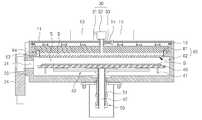
도 2는 본 발명의 일 실시 예에 따른 평면디스플레이용 화학 기상 증착장치의 구조도이다.2 is a structural diagram of a chemical vapor deposition apparatus for a planar display according to an embodiment of the present invention.
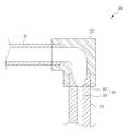
도 3은 본 발명의 일 실시 예에 따른 평면디스플레이용 화학 기상 증착장치의 가스유입부의 단면도이다.3 is a cross-sectional view of a gas inlet of the chemical vapor deposition apparatus for a flat display according to an embodiment of the present invention.
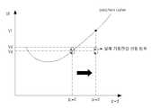
도 4는 파센곡선을 도시한 도면이다.4 is a diagram illustrating a Fassen curve.
* 도면의 주요 부분에 대한 부호의 설명* Explanation of symbols for the main parts of the drawings
1 : 평면디스플레이용 화학 기상 증착장치1: Chemical vapor deposition apparatus for flat panel display
10 : 상부 챔버 11 : 상판부10: upper chamber 11: top plate
13 : 가스공급부 15 : 고주파 전원부13
20 : 하부 챔버 30 : 가스유입부20: lower chamber 30: gas inlet
31 : 가스피드스루관 32 : 앵글어댑터31 gas feed-
33 : 가스유입관 34 : 기생 플라즈마 발생저지부33: gas inlet pipe 34: parasitic plasma generation stop
35 : 기생 플라즈마 발생저지부의 제1 구간35: first section of the parasitic plasma generation blocking unit
36 : 기생 플라즈마 발생저지부의 제2 구간36: second section of the parasitic plasma generation blocking unit
50 : 승강 모듈 60 : 전극50: elevating module 60: electrode
61 : 후방 플레이트 62 : 가스분배판61
본 발명은, 평면디스플레이용 화학 기상 증착장치에 관한 것으로서, 보다 상세하게는, 가스유입관의 컨덕턴스를 감소시켜 앵글어댑터 영역의 압력을 증가하도록 유도하여 가스피드스루관 내의 기생 플라즈마 발생을 저지시키는 디스플레이용 화학 기상 증착장치에 관한 것이다.BACKGROUND OF THE INVENTION 1. Field of the Invention The present invention relates to a chemical vapor deposition apparatus for planar displays, and more particularly, a display for preventing parasitic plasma generation in a gas feedthrough tube by reducing conductance of a gas inlet pipe to increase pressure in an angle adapter region. A chemical vapor deposition apparatus for the present invention.
최근 들어 반도체 산업 중 전자 디스플레이 산업이 급속도로 발전하면서 평면디스플레이(Flat Panel Display, FPD)가 등장하기 시작하였다.Recently, the flat panel display (FPD) has begun to emerge as the electronic display industry is rapidly developing among the semiconductor industry.
평면디스플레이(FPD)는, TV나 컴퓨터 모니터 등에 디스플레이(Display)로 주로 사용된 음극선관(CRT, Cathode Ray Tube)보다 두께가 얇고 가벼운 영상표시장치인데, 종류로는 액정표시장치(LCD, Liquid Crystal Display), 플라즈마 디스플레이 패널(PDP, Plasma Display Panel) 및 유기EL(OLED, Organic Light Emitting Diodes) 등이 있다.A flat panel display (FPD) is an image display device that is thinner and lighter than a cathode ray tube (CRT), which is mainly used as a display for a TV or a computer monitor, and is a liquid crystal display device (LCD, Liquid Crystal). Display, Plasma Display Panel (PDP) and Organic Light Emitting Diodes (OLED).
평면디스플레이 중 대표격인 액정표시장치(LCD)는, 2장의 얇은 상하 유리기판 사이에 고체와 액체의 중간물질인 액정을 주입하고, 상하 유리기판의 전극 전압 차로 액정분자의 배열을 변화시킴으로써 명암을 발생시켜 숫자나 영상을 표시하는 일종의 광스위치 현상을 이용한 소자이다.Among the flat panel displays, a liquid crystal display (LCD) generates a contrast by injecting a liquid crystal, which is an intermediate material between a solid and a liquid, between two thin upper and lower glass substrates, and changing the arrangement of liquid crystal molecules by the difference in electrode voltage between the upper and lower glass substrates. It is a device using a kind of optical switch phenomenon that displays numbers or images.
이러한 액정표시장치(LCD)는 박형화, 경량화, 저소비전력화를 기술적으로 구현함으로써 종래의 음극선관(CRT)이 적용될 수 없었던 노트북 PC, 전자계산기, 각종 전자제품 등의 디스플레이로 사용되고 있으며, 기존의 음극선관을 빠른 속도로 대체하고 있다. 이들 중에 LCD TV는 종래에는 20 인치 내지 30 인치 정도의 크기를 가지며, 컴퓨터 모니터는 17 인치 이하의 크기를 갖는 것이 주류였다. 그러나, 최근에는 40 인치 이상의 대형 TV와 20 인치 이상의 대형 모니터에 대한 선호도가 높아지고 있다.The liquid crystal display (LCD) is being used as a display for laptop PCs, electronic calculators, and various electronic products, in which a conventional cathode ray tube (CRT) could not be applied by technically implementing thinner, lighter, and lower power consumption. Is rapidly replacing. Among them, LCD TVs conventionally have a size of about 20 inches to about 30 inches, and computer monitors have a mainstream size of 17 inches or less. Recently, however, preference for large TVs of 40 inches or larger and large monitors of 20 inches or larger has increased.
따라서 액정표시장치(LCD)를 구성하는 유리기판의 경우, 보다 넓은 크기로 제작하기에 이르렀다. 현재에는 가로/세로의 폭이 1870 ㅧ 2200 ㎜이거나 1870 ㅧ 2250 ㎜인 7세대가 사용되며, 2160 ㅧ 2460 ㎜ 이상인 8세대까지 유리기판의 크기를 증가시키는 연구가 진행되고 있으며 8세대 유리기판의 생산을 목전에 두고 있다.Therefore, the glass substrate constituting the liquid crystal display (LCD) has been produced in a wider size. Currently, 7th generation with width of 1870 ㅧ 2200 ㎜ or 1870 ㅧ 2250 ㎜ is used, and research is being conducted to increase the size of glass substrates to 8 generations of 2160 2460 ㎜ or more. Is in sight.
한편, 액정표시장치(LCD)는 증착(Deposition), 사진공정(Photo lithography), 식각(Etching), 플라즈마 강화 화학 기상 증착(Plasma Enhanced Chemical Vapor Deposition, 이하 화학 기상 증착이라 한다) 등의 공정이 반복적으로 수행되는 TFT공정, 상하 유리기판을 합작하는 Cell공정, 그리고 기구물을 완성하는 Module공정을 통해 제품으로 출시된다.On the other hand, the liquid crystal display (LCD) is repeatedly a process such as deposition, photo lithography, etching, plasma enhanced chemical vapor deposition (hereinafter referred to as chemical vapor deposition) It is released as a product through the TFT process, Cell process of jointing up and down glass substrates, and Module process of completing instruments.
이들 공정 중의 하나인 화학 기상 증착공정(Chemical Vapor Deposition Process)은, 외부의 고주파 전원에 의해 플라즈마(Plasma)화 되어 높은 에너지를 갖는 실리콘계 화합물 이온(ion) 가스가 전극을 통해 가스분배판으로부터 분출되어 유리기판 상에 증착되는 공정이다. One of these processes, the chemical vapor deposition process, is plasma-formed by an external high frequency power source, and silicon-based compound ion gas having high energy is ejected from the gas distribution plate through the electrode. It is a process deposited on a glass substrate.
도 1은 종래의 일 실시 예에 따른 평면디스플레이용 화학 기상 증착장치의 가스유입부(130)의 단면도이다.1 is a cross-sectional view of a
화학 기상 증착장치는, 공정 챔버(미도시) 내에서 플라즈마(Plasma)화 된 이온 가스(gas) 즉, 공정 가스(gas)를 공정 챔버(미도시) 내부로 유입시키기 위한 가스유입부(130)가 상부 챔버(미도시)의 상단에 마련된다.The chemical vapor deposition apparatus includes a
가스유입부(130)에는, 도 1에 도시된 바와 같이, 가스공급부(미도시)에서 생성된 공정 가스(gas)를 챔버(미도시) 내부로 유입시키기 위한 가스유입관(133)과 공정 가스(gas)를 가스유입관(133)으로 이송시키는 가스피드스루관(131)과, 공정 가스(gas)의 이동 경로를 가변시키는 앵글어댑터(132)가 구비된다. 여기서 공정 가스(gas)가 통과하는 가스피드스루관(131) 및 앵글어댑터(132) 및 가스유입관(133)의 내경은 모두 동일하다.As shown in FIG. 1, the
이와 같이, 가스공급부(미도시)로부터 공급되는 공정 가스(gas)는 가스유입부(130)를 통해 챔버 내부의 후방플레이트(미도시)와 가스분배판(미도시) 사이의 버퍼공간(미도시)으로 공급될 수 있고, 챔버 내부로 공급된 공정 가스(gas)는 고주파 전원에 의해 플라즈마화 되어 유리기판(G) 상에 증착되게 된다.As such, the process gas supplied from the gas supply unit (not shown) is a buffer space (not shown) between the rear plate (not shown) and the gas distribution plate (not shown) inside the chamber through the
한편, 플라즈마의 발생은 파센곡선(Paschen Curve)을 따른다. 파센곡선은 압력(p)과 전극 간 거리(d)에 따른 초기 방전 전압(Vf)을 도시하는데 일반적인 화학 기상 증착장치에서는 압력(p)과 전극 간 거리(d)의 곱(pd, 이하 pd 값이라 한다)이 초기 방전 전압(Vf)과 비례한다.On the other hand, the generation of the plasma follows the Paschen Curve. The Fassen curve shows the initial discharge voltage (Vf) according to the pressure (p) and the distance between the electrodes (d) .In a typical chemical vapor deposition apparatus, the product of the pressure (p) and the distance (d) between the electrodes (pd, hereinafter pd) Is proportional to the initial discharge voltage Vf.
그런데, 종래의 화학 기상 증착장치에서는, 공정 가스가 접지 쪽에서 고주파 전원 측으로 인입될 때 특정 조건에서 고주파 전원이 인가되면 가스피드스루관(131) 내부에 기생 플라즈마가 발생될 수 있고, 이로 인해 가스피드스루관(131) 내부 및 이와 연결되는 구조물에 손상이 야기될 수 있을 뿐만 아니라, 파티클(particle)이 발생되어 증착 공정 결과에 직접적으로 악영향을 미치는 문제점이 있다.However, in the conventional chemical vapor deposition apparatus, when a high frequency power is applied under a specific condition when the process gas is drawn from the ground side to the high frequency power side, parasitic plasma may be generated inside the
따라서 본 발명의 목적은, 가스피드스루관 내의 기생플라즈마 발생을 저지함으로써 가스유입부의 손상을 방지할 수 있으며 또한 파티클 발생을 저지하여 공정 수율이 향상될 수 있는 평면디스플레이용 화학 기상 증착장치를 제공하는 것이다.Accordingly, an object of the present invention is to provide a chemical vapor deposition apparatus for planar displays, which can prevent the gas inlet from being damaged by preventing parasitic plasma generation in the gas feed-through tube and also prevent the generation of particles to improve the process yield. will be.
상기 목적은, 본 발명에 따라, 평면디스플레이에 대한 증착 공정이 진행되는 챔버; 상기 챔버 내로 상기 증착 공정을 위한 공정 가스를 유입시키는 가스유입관; 상기 가스유입관과 연결되며, 상기 공정 가스를 상기 가스유입관으로 이송시키는 가스피드스루관; 및 상기 가스유입관에 마련되며, 상기 가스피드스루관의 압력을 증가시켜 상기 증착 공정 시 상기 가스피드스루관의 내벽에 기생 플라즈마가 발생되는 것을 저지하는 기생 플라즈마 발생저지부를 포함하는 것을 특징으로 하는 평면디스플레이용 화학 기상 증착장치에 의해 달성된다.The object is, according to the present invention, a chamber in which a deposition process for a flat panel display proceeds; A gas inlet pipe for introducing a process gas for the deposition process into the chamber; A gas feed-through pipe connected to the gas inlet pipe and transferring the process gas to the gas inlet pipe; And a parasitic plasma generation blocking unit provided in the gas inlet pipe and increasing a pressure of the gas feed through pipe to prevent parasitic plasma from being generated on an inner wall of the gas feed through pipe during the deposition process. It is achieved by a chemical vapor deposition apparatus for planar displays.
상기 기생 플라즈마 발생저지부는, 상기 가스유입관의 내면에 마련되되 적어도 일부 구간이 상기 가스피드스루관의 내경보다 작게 형성되는 상기 가스유입관의 내면 형상일 수 있다.The parasitic plasma generation stopper may be provided on an inner surface of the gas inlet pipe, and may have an inner surface shape of the gas inlet pipe having at least a partial section smaller than an inner diameter of the gas feed-through pipe.
상기 가스유입관의 내면 형상은, 상기 가스유입관의 길이 방향을 따라 상기 가스피드스루관 측으로부터 상기 가스유입관의 일 영역까지 형성되는 제1 구간; 및 상기 제1 구간과는 내면이 상이하게 형성되되, 상기 제1 구간이 끝나는 지점에서 상기 챔버까지 형성되는 제2 구간을 포함할 수 있다.The inner surface of the gas inlet pipe may include a first section formed from a side of the gas feed through pipe to a region of the gas inlet pipe along a length direction of the gas inlet pipe; And a second section having an inner surface different from the first section, and formed from the point where the first section ends to the chamber.
상기 제1 구간은 경사진 형상이고, 상기 제2 구간은 직선 형상을 갖는 것일 수 있다.The first section may have an inclined shape, and the second section may have a straight shape.
상기 제1 구간은, 상기 가스유입관의 길이 방향을 따라 상기 제2 구간 측으로 갈수록 점진적으로 그 내경이 작아지게 상기 제2 구간까지 경사지게 형성될 수 있다.The first section may be formed to be inclined to the second section to gradually decrease the inner diameter toward the second section side along the longitudinal direction of the gas inlet pipe.
상기 제2 구간의 내경은 상기 가스피드스루관의 내경 대비 15 퍼센트(%) 내지 95 퍼센트(%)의 범위를 갖는 것일 수 있다.The inner diameter of the second section may be in the range of 15 percent (%) to 95 percent (%) of the inner diameter of the gas feed-through tube.
상기 가스피드스루관과 상기 가스유입관은 상호 교차 배치되되, 상기 가스피드스루관과 상기 가스유입관 사이에는 관의 경로를 가변시키는 앵글어댑터가 더 마련될 수 있다.The gas feed-through pipe and the gas inlet pipe may be disposed to cross each other, and an angle adapter may be further provided between the gas feed-through pipe and the gas inlet pipe to vary the path of the pipe.
상기 기생 플라즈마 발생저지부는, 적어도 일 영역에서 굽은 곡선 형상을 갖는 가스유입관일 수 있다.The parasitic plasma generation preventing unit may be a gas inlet pipe having a curved shape at least in one region.
상기 가스피드스루관은 세라믹 재질로 형성되고, 상기 가스유입관은 알루미 늄 재질로 형성될 수 있다.The gas feed-through tube may be formed of a ceramic material, and the gas inlet tube may be formed of aluminum.
상기 평면디스플레이는 LCD용 유리기판일 수 있다.The flat panel display may be a glass substrate for LCD.
본 발명과 본 발명의 동작상의 이점 및 본 발명의 실시에 의하여 달성되는 목적을 충분히 이해하기 위해서는 본 발명의 바람직한 실시 예를 예시하는 첨부 도면 및 첨부 도면에 기재된 내용을 참조하여야만 한다.In order to fully understand the present invention, the operational advantages of the present invention, and the objects achieved by the practice of the present invention, reference should be made to the accompanying drawings which illustrate preferred embodiments of the present invention and the contents described in the accompanying drawings.
이하, 첨부된 도면을 참조하여 본 발명의 바람직한 실시 예를 설명함으로써, 본 발명을 상세히 설명한다. 각 도면에 제시된 동일한 참조부호는 동일한 부재를 나타낸다.Hereinafter, exemplary embodiments of the present invention will be described in detail with reference to the accompanying drawings. Like reference numerals in the drawings denote like elements.
도 2는 본 발명의 일 실시 예에 따른 평면디스플레이용 화학 기상 증착장치의 구조도이고, 도 3은 본 발명의 일 실시 예에 따른 평면디스플레이용 화학 기상 증착장치의 가스유입부의 단면도이다.2 is a structural diagram of a chemical vapor deposition apparatus for a planar display according to an embodiment of the present invention, Figure 3 is a cross-sectional view of the gas inlet of the chemical vapor deposition apparatus for a planar display according to an embodiment of the present invention.
설명에 앞서, 평면디스플레이(Flat Display)란, 전술한 바와 같이 LCD(Liquid Crystal Display), PDP(Plasma Display Panel) 및 OLED(Organic Light Emitting Diodes) 중 어떠한 것이 적용되어도 좋다.Prior to the description, any of flat liquid display (LCD), plasma display panel (PDP), and organic light emitting diodes (OLED) may be applied to the flat display.
다만, 본 실시 예에서는 LCD(Liquid Crystal Display)용 대형 유리기판을 평면디스플레이로 간주하여 설명하기로 한다. 여기서 대형이란, 앞서도 기술한 바와 같이, 8세대에 적용되는 수준의 크기를 가리킨다. 이하, 평면디스플레이를 유리기판(G)이라 명칭하여 설명하기로 한다.However, in the present embodiment, a large glass substrate for an LCD (Liquid Crystal Display) will be described as a flat display. As described above, the large size refers to the size of the level applied to the eighth generation. Hereinafter, the flat panel display will be referred to as a glass substrate (G).
도 2 에 도시된 바와 같이, 본 발명의 일 실시 예에 따른 평면디스플레이용 화학 기상 증착장치(1)는, 유리기판(G)에 대한 증착 공정이 진행되는 상부 챔 버(10) 및 하부 챔버(20)와, 상부 챔버(10) 내에 마련되어 증착 대상물인 유리기판(G)을 향해 소정의 실리콘계 화합물 이온인 증착 물질 즉 플라즈마(plasma)화된 공정 가스(gas)를 방출하되 상부 전극 역할을 하는 전극(60)과, 하부 챔버(20) 내에 마련되어 유리기판(G)이 로딩(Loading)되는 서셉터(40)와, 서셉터(40)의 하부에서 서셉터(40)를 지지하는 서셉터지지대(43)를 포함한다.As shown in FIG. 2, the chemical vapor deposition apparatus 1 for a flat panel display according to an embodiment of the present invention includes an
여기서 상부 챔버(10) 및 하부 챔버(20)는 한 몸체를 이루어 그 내부의 증착공간(S)에서 유리기판(G)에 대한 증착 공정이 진행될 때 증착공간(S)이 진공 분위기로 유지될 수 있도록 증착공간(S)은 증착 공정 시 외부로부터 차폐된다.Here, the
상부 챔버(10)에 대해 자세히 살펴보면, 도 2에 도시된 바와 같이, 상부 챔버(10)의 내부에 횡 방향을 따라 전극(60)이 구비되어 있다. 전극(60)은, 버퍼공간(B)을 사이에 두고 상부 챔버(10)의 내측에 결합되는 후방플레이트(61)와, 하부 챔버(20)를 향한 전면에 배치되는 가스분배판(62)을 구비한다.Looking in detail with respect to the
후방플레이트(61)는, 가스공급부(13)로부터 공정 가스(gas)가 공급될 수 있도록 그 중앙 영역이 관통 형성되어 있으며, 관통 형성된 부분에는 가스유입관(33)이 결합되어 있다. 후방플레이트(61) 및 후방플레이트(61)와 결합된 가스분배판(62)은 가스공급부(13)로부터 공급되는 공정 가스(gas)가 플라즈마화 될 수 있도록 고주파 전원부(15)와 연결라인(14)에 의해 전기적으로 연결되어 있다.The
또한 가스분배판(62)에는 가스분배판(62)의 상부와 하부를 관통하는 복수 개의 가스통과공(미도시)이 마련되는데, 이 가스통과공(미도시)을 통해 공정 가스(gas)가 유리기판(G) 상에 증착된다.In addition, the
이러한 후방플레이트(61)와 가스분배판(62) 사이에는 현가지지부재(63)가 마련되어 있다. 현가지지부재(63)는 버퍼공간(B) 내의 플라즈마화된 공정 가스(gas)가 외부로 누출되지 않도록 할 뿐만 아니라 수백 킬로그램 정도의 무게를 갖는 가스분배판(62)을 후방플레이트(61)에 현가 지지하는 역할을 담당한다. 뿐만 아니라 현가지지부재(63)에는 증착 공정 시 수백도 가령 200℃ 정도로 가열되는 가스분배판(62)이 X축, Y축 및 Z축 중 적어도 어느 한 방향으로 열팽창하는 것을 보상하는 역할도 겸한다.A
또한 후방플레이트(61) 및 가스분배판(62)로부터 상부 챔버(10)의 벽으로 전기가 통하는 것을 저지하기 위하여, 도 2에 도시된 바와 같이, 후방플레이트(61)와 상부 챔버(10)의 벽 사이, 그리고 가스분배판(62)과 상부 챔버(10)의 벽 사이에 테프론(Tefron) 재질의 인슐레이터(64)가 마련된다.Also, in order to prevent electricity from flowing from the
상부 챔버(10)의 상단에는 상판부(11)가 구비되어 있다. 상판부(11)는 상부 챔버(10)의 상부를 덮는 역할을 한다. 상판부(11)상에는, 상부 챔버(10)의 상판부(11)에 결합되어 전극(60)에 의해 형성되는 증착공간(S)으로 플라즈마화된 공정 가스(gas)를 제공하는 가스공급부(13) 및 가스공급부(13)로부터 실제 증착 공정이 이루어지는 공정 챔버(10, 20) 내부로 공정 가스(gas)를 유입시키는 연결 통로인 가스유입부(30) 및 고주파 전원부(15)가 구비된다. 여기서, 가스유입부(30)에 대한 설명은 자세히 후술하기로 한다.The
하부 챔버(20)에 대해서 살펴보면, 하부 챔버(20)는, 실질적으로 유리기판(G)에 대한 증착 공정이 진행되는 부분으로서, 전술한 증착공간(S)이 하부 챔 버(20) 내에 형성된다. 이러한 하부 챔버(20)의 외벽에는 소정의 작업 로봇(미도시)에 의해 유리기판(G)이 증착공간(S) 내외로 출입할 수 있도록 기판출입부(21)가 형성되어 있다. 이러한 기판출입부(21)는 그 주변에 결합된 도어(24)에 의해 선택적으로 개폐된다.Referring to the
도시하지는 않았지만, 하부 챔버(20) 내의 바닥면 영역에는 증착공간(S)에 존재하는 공정 가스(gas)를 다시 증착공간(S)으로 확산시키는 가스확산판(미도시)이 마련되어 있다.Although not shown, a gas diffusion plate (not shown) is provided in the bottom region of the
서셉터(40, Susceptor)는 하부 전극 역할을 함과 동시에 하부 챔버(20) 내의 증착공간(S)에서 횡 방향으로 배치되어 로딩(loading)되는 유리기판(G)을 지지한다. 보통은 증착 대상물인 유리기판(G)의 면적보다 큰 구조물로 형성되며, 서셉터(40)의 상면은 유리기판(G)이 정밀하게 수평 상태로 로딩될 수 있도록 거의 정반으로 제조된다.The
서셉터(40)의 상면으로 유리기판(G)이 얹혀지면서 로딩되거나 취출되기 위해 서셉터(40)에는 로딩되거나 취출되는 유리기판(G)의 하면을 안정적으로 지지하는 복수의 리프트 핀(41)이 더 구비되어 있다. 리프트 핀(41)들은 서셉터(40)를 관통하도록 서셉터(40)에 설치되어 있다.The plurality of lift pins 41 stably supporting the bottom surface of the glass substrate G loaded or taken out on the
이러한 리프트 핀(41)들은 서셉터(40)가 하강할 때, 그 하단이 하부 챔버(20)의 바닥면에 가압되어 상단이 서셉터(40)의 상단으로 돌출된다. 리프트 핀(41)의 돌출된 상단은 유리기판(G)을 상부로 들어올리게 되고 따라서 유리기판(G)은 서셉터(40)로부터 이격되게 된다. 서셉터(40)가 부상하면, 리프트 핀(41) 이 서셉터(40)의 상면에 대해 하방으로 이동하여 유리기판(G)이 서셉터(40)의 상면에 밀착된다. 즉, 리프트 핀(41)들은 로봇아암(미도시)이 서셉터(40)에 로딩된 유리기판(G)을 파지할 수 있도록 유리기판(G)과 서셉터(40) 사이의 공간을 형성하는 역할을 겸한다.When the
이러한 서셉터(40)에는, 그 상단이 배면 중앙 영역에 고정되고 하단이 하부 챔버(20)를 통해 하방으로 노출되어 서셉터(40)를 승강 가능하게 지지하는 컬럼(42)이 더 결합되어 있다.The
전술한 바와 같이, 8세대 하에서의 서셉터(40)는 무겁고 사이즈(size) 또한 크기 때문에 처짐 등이 발생될 수 있는데, 이는 서셉터(40)의 상면에 로딩되는 유리기판(G)의 처짐 등으로 연계될 수 있다. 이에, 도 2에 도시된 바와 같이, 컬럼(42)의 상부 영역에는 서셉터 지지부(43)가 마련되어 서셉터(40)를 안정적으로 떠받치고 있다.As described above, the
서셉터(40)는 하부 챔버(20) 내의 증착공간(S)에서 상하로 승강한다. 즉, 유리기판(G)이 로딩될 때는 하부 챔버(20) 내의 바닥면 영역에 배치되어 있다가 유리기판(G)이 서셉터(40)의 상면에 밀착되고 증착 공정이 진행될 때에는 유리기판(G)이 후술할 가스분배판(62)에 인접할 수 있도록 부상한다. 이를 위해, 서셉터(40)에 결합된 컬럼(42)에는 서셉터(40)를 승강시키는 승강 모듈(50)이 더 마련되어 있다.The
승강 모듈(50)에 의해 서셉터(40)가 승강하는 과정에서 컬럼(42)과 하부 챔버(20) 사이에 공간이 발생되면 안 된다. 따라서 컬럼(42)이 통과하는 하부 챔버(20)의 해당 영역에는 컬럼(42)의 외부를 감싸도록 벨로우즈관(51)이 마련되어 있다. 벨로우즈관(51)은 서셉터(40)가 하강할 때 팽창되고, 서셉터(40)가 부상할 때 압착된다.In the process of elevating the
전술한 바와 같이, 상판부(11)에는, 상부에 플라즈마화된 공정 가스(gas)를 공급시키기 위한 가스공급부(13)와, 가스유입부(30)와, 챔버(10) 내에 결합되어 있는 후방플레이트(61)와 연결라인(14)에 의해 전기적으로 연결되어 있는 고주파 전원부(15)가 설치된다.As described above, the
가스유입부(30)에 대해 자세히 설명하면, 도 2 및 도 3에 도시된 바와 같이, 가스유입부(30)는, 가스유입관(33)과, 가스공급부(13)와 가스유입관(33)이 연결되도록 가스공급부(13) 및 고주파 전원부(15) 사이에 마련되어 가스공급부(13)로부터 유입되는 공정 가스(gas)의 이동 경로가 되는 가스피드스루관(31)과, 가스유입관(33) 및 가스피드스루관(31) 사이에 마련되어 공정 가스의 이동 경로를 가변시키는 앵글어댑터(32)를 구비한다.Referring to the
가스피드스루관(31)은 속이 빈 튜브 형태로서, 그 일단은 가스공급부(13)에 연결되고, 타단은 앵글어댑터(32)에 연결된다.The gas feed-through
도 2 및 도 3을 참조하면, 가스공급부(13)로부터 챔버(10) 내의 후방플레이트(61)로 공정 가스(gas)를 이송시키는 이동 경로가 되는 앵글어댑터(32)가 대략 'ㄱ'자형으로 형성된다. 앵글어댑터(32)의 일단은 가스피드스루관(31)의 일단과 결합되고, 타단은 가스유입관(33)의 일단에 결합된다.2 and 3, the
가스유입관(33)의 일단은 앵글어댑터(32)의 하단과 결합되고, 타단은 챔버 내의 후방플레이트(61)에 결합되어 앵글어댑터(32)를 통과한 공정 가스(gas)가 가 스유입관(33)을 지나 공정 챔버(10, 20) 내부로 유입된다. 그리고 전술한 앵글어댑터(32)와 가스유입관(33)은 알루미늄 소재의 도전체로 제작되어 고주파 전원부(15)로부터 발생된 고주파 전원이 전기적으로 통전된다.One end of the
이러한 구성에 의해 가스공급부(13)로부터 공급되는 공정 가스(gas)가 가스피드스루관(31)과 앵글어댑터(32), 그리고 가스유입관(33)을 각각 차례대로 통과하여 버퍼공간(B)으로 공급될 수 있고, 후방플레이트(61)가 고주파 전원부(15)에 의해 공급되는 고주파 전력에 의해 전극을 띠게 됨으로써 버퍼공간(B)으로 유입된 공정 가스(gas)를 플라즈마화 할 수 있다.By this configuration, the process gas supplied from the
그런데, 종래의 가스유입부(130)는, 전술한 바와 같이, 가스피드스루관(131) 및 앵글어댑터(132) 및 가스유입관(133)의 내경이 모두 동일하도록 마련되어, 증착 공정 시 특정 조건하에서 가스피드스루관(31) 내부에서 발생되는 기생 플라즈마에 의해 내부 구조물이 손상되는 문제점이 있었고, 또한 이로 인해 발생되는 파티클 때문에 공정 결과에 직접적인 악영향을 미치는 문제가 있었다.However, as described above, the conventional
여기서 먼저 가스피드스루관(31) 내부의 기생 플라즈마 발생의 원인을 살펴 보면, 기생 플라즈마 발생 현상은 도 4에 도시된 파센곡선의 방전 개시 전압(Vf)과 관련하여 설명할 수 있다.Here, looking at the cause of the parasitic plasma generation in the gas feed-through
일반적으로 플라즈마 발생은 파센곡선을 따르게 된다. 파센곡선은 두 전극 간 거리(d)와 압력(p)의 곱과, 방전 개시 전압(Vf)과의 상관 관계를 도시한다. 따라서 도 4를 살펴보면 전극 간 거리(d) 및 압력(p)의 곱(이하, pd 값이라 한다.)이 클 경우 pd 값에 비례하여 플라즈마가 생성될 방전 개시 전압(Vf)이 증가됨을 알 수 있다.In general, plasma generation follows a Parssen curve. The Fassen curve shows the product of the distance d between the two electrodes and the pressure p and the correlation between the discharge start voltage Vf. Therefore, referring to FIG. 4, when the product of the distance between the electrodes d and the pressure p (hereinafter, referred to as pd value) is large, it can be seen that the discharge start voltage Vf at which the plasma is generated increases in proportion to the pd value. have.
기생 플라즈마가 발생하는 특정 조건에 대해서 파센 곡선을 참조해서 설명하면, 실제 전극에 걸리는 가동 전압(Va) 또는 가동 전압의 변동 상한값(Va')이, 임의의 pd 값에 대응되는 방전 개시 전압(Vf)보다 큰 상태를 의미하고, 이런 조건 하에서 가동 전압(Va) 또는 가동 전압의 변동 상한값(Va')이 플라즈마를 생성시킬 시의 방전 개시 전압(Vf)보다 크게 되므로 기생 플라즈마가 발생된다. The specific conditions under which the parasitic plasma is generated will be described with reference to the Passen curve. The discharge starting voltage Vf at which the operating voltage Va or the upper limit variation of the operating voltage Va 'applied to the actual electrode corresponds to an arbitrary pd value is described. ), And under these conditions, the parasitic plasma is generated because the operating voltage Va or the upper limit value of change Va 'of the operating voltage becomes larger than the discharge start voltage Vaf at the time of generating the plasma.
한편, 보통 화학 기상 증착장치(1)에서는, 구조적인 어려움, 구속 조건 등의 여러 가지 제약으로 인해, 고주파 전원부(15)와 연결되어 고주파 전원이 걸리는 측과 접지부 간의 전극 거리(d)는 변동시키기가 쉽지 않다. 또한 실제 증착 공정 시에 고주파 전원부(15)로부터 공급되어 전극에 걸리는 가동 전압(Va)도 한번 설정되면 변화시키기가 쉽지 않다. 결국 플라즈마의 발생 여부는 압력(p)에 의존하게 되며, 압력(p)의 증가는 이에 비례하여 방전 개시 전압(Vf)의 증가를 수반한다.On the other hand, in the chemical vapor deposition apparatus 1, due to various constraints such as structural difficulties and constraints, the electrode distance d between the side connected to the high
따라서 방전 개시 전압(Vf)를 증가시켜 가스피드스루관(31) 내에 기생 플라즈마 발생되는 것을 저지시키기 위한 방안으로서, 가스피드스루관(31)에 걸리는 압력(p1)을 증가시킬 필요가 있다. 압력(p1)을 증가시키면 자연히 pd 값이 증가하게 되고 이로 인해 결정되는 방전 개시 전압(Vf) 또한 상승하게 된다. 따라서 증가된 방전 개시 전압(Vf)이 실제 증착 공정 시 걸리는 가동 전압(Va)보다 큰 값으로 조정되어 기생 플라즈마의 발생이 억제될 수 있다.Therefore, it is necessary to increase the pressure p1 applied to the gas feed through
다시 말해, 가스피드스루관(31)의 압력(p1)을 증가시켜 pd 값을 증가시키게 되면 플라즈마가 발생되는 최초 임계치인 방전 개시 전압(Vf) 값이 증가된다. 따라 서 방전 개시 전압(Vf)이 가동 전압(Va) 및 가동 전압의 변동 상한값(Va')보다 더 큰 값으로 조정되는 결과 증착 공정 시에는 방전 개시 전압(Vf)에 도달하지 못하므로 가스피드스루관(31) 내부에 플라즈마 생성이 저지될 수 있다.In other words, when the pressure p1 of the gas feed-through
따라서 기생 플라즈마가 생성되는 것을 저지하기 위해서는 가스피드스루관(31)의 압력(p1) 증가를 요한다. 압력(p1)을 증가시킬 방안과 관련하여 진공 유관에서의 유량(Q)과 압력(p) 그리고 컨덕턴스(C, Conductance, 시간당 흐를 수 있는 가스량)와의 관계를 살펴볼 필요가 있다.Therefore, in order to prevent generation of parasitic plasma, it is necessary to increase the pressure p1 of the gas feed-through
일반적으로 진공 상태의 유관에서는, 유입되는 가스량(Q), 가스피드스루관(31)의 압력(p1), 공정 챔버(10, 20) 내의 압력(p2), 유로가 좁아진 가스유입관(33)의 컨덕턴스(C)와의 관계는 Q = C X (p1 - p2)와 같은 수학식으로 표현될 수 있다. 가스공급부(13)로부터 공급되는 시간당 유입되는 공정 가스량(Q)과 증착 공정이 진행되는 챔버(10, 20) 내의 압력(p2)은 고정되므로, 가스피드스루관(31)의 압력(p1)과 컨덕턴스(C)와의 관계는 서로 반비례하게 된다.In general, in a vacuum flow pipe, the amount of gas flowing in (Q), the pressure p1 of the gas feed-through
즉, 상부 및 하부 챔버(10, 20) 내의 압력(p2) 및 공정 가스량(Q)이 일정하다면, 가스피드스루관(31)의 압력(p1)은 공정 챔버(10, 20) 내의 압력(p2)과 진공 상태가 형성되는 가스피드스루관(31)과 공정 챔버(10, 20) 사이의 유관 즉, 가스유입관(33)의 컨덕턴스(C)에 의해 결정된다. 따라서 유입되는 공정 가스량(Q)이 일정할 경우 컨덕턴스(C)가 작아질수록 가스피드스루관(31)의 압력(p1)은 높아진다.That is, if the pressure p2 and the process gas amount Q in the upper and
따라서 가스피드스루관(31)과 챔버(10, 20) 사이의 유로를 축소시키면 컨덕턴스(C)가 감소하게 되고 이에 반비례하게 가스피드스루관(31)의 압력(p1)이 증가 될 수 있다. 이를 통해 가스피드스루관(31)의 내부 영역에 기생 플라즈마 발생이 저지될 수 있다.Therefore, when the flow path between the gas feed-through
따라서, 본 발명의 일 실시 예에서는, 도 2 및 도 3에 도시된 바와 같이, 상부 및 하부 챔버(10, 20) 내로 증착 공정을 위한 공정 가스(gas)를 유입시키는 가스유입관(33) 내에, 가스피드스루관(31)의 압력(p1)을 증가시키기 위한 기생 플라즈마 발생저지부(34)가 마련된다.Therefore, in one embodiment of the present invention, as shown in Figures 2 and 3, in the
본 실시 예에서 기생 플라즈마 발생저지부(34)는, 가스피드스루관(31)의 내경보다 작게 형성되는 가스유입관(33)의 내면 형상(34)으로서, 가스유입관(33)의 내면 형상(34)은, 가스유입관(33)의 길이 방향을 따라 가스피드스루관(31) 측으로부터 가스유입관(33)의 일 영역까지 형성되는 제1 구간(35)과, 제1 구간(35)과는 내면이 상이하게 형성되되, 제1 구간(35)이 끝나는 지점에서 공정 챔버(10, 20)까지 형성되는 제2 구간(36)을 포함한다.In the present embodiment, the parasitic plasma
가스유입관(33)의 내면 형상(34)의 제1 구간(35)은, 가스유입관(33)의 길이 방향을 따라 제2 구간(36) 측으로 갈수록 점진적으로 그 내경이 작아지도록 테이퍼지게 형성되고, 가스유입관(33)의 내면 형상(34)의 제2 구간(36)은 직선형으로 형성된다. 여기서 제2 구간(36)의 내경은 가스피드스루관(31)의 내경 대비 15 퍼센트(%)에서 95 퍼센트(%)가 되도록 형성할 수 있으며, 본 실시 예에서는 60 퍼센트(%)가 되도록 형성된다.The
이와 같이 가스유입관(33)의 내경을 가스피드스루관(31) 및 앵글어댑터(32)의 내경보다 상대적으로 작게 형성되도록 함으로써 가스피드스루관(31) 영역의 압 력(p1) 상승 효과를 얻을 수 있다.As such, the inner diameter of the
또한, 가스유입관(33)의 내면 형상(34)의 제1 구간(35)의 테이퍼진 형상은, 가스유입관(33) 내부에 유입된 공정 가스(gas)의 유속을 빠르게 하는 역할을 하는 한편, 내경을 완만하게 감소시킴으로써 공정 가스(gas)의 흐름이 층류(Laminar flow)가 유지되어 공정 가스의 이송이 원활히 이루어지도록 한다. 또한 제1 구간(35)은 유로 상의 싱크(sink) 역할을 수행하여 가스피드스루관(31) 및 앵글어댑터(32)의 내부 영역에 공정 가스(gas)의 잔여물을 제거하는 역할도 겸한다. In addition, the tapered shape of the
이와 같이 가스유입관(33)의 내경을 가스피드스루관(31)대비 15 퍼센트 내지 95 퍼센트로 마련하여 가스유입관(33)의 컨덕턴스(C)를 줄이게 되면, 가스피드스루관(31)의 압력(p1)을 증가시킬 수 있고 가스피드스루관(31)의 압력(p)이 증가되면 이에 대응되는 방전 개시 전압(Vf)을 증가시킬 수 있어, 종국적으로 가스피드스루관(31) 내의 기생 플라즈마 발생을 저지시킬 수 있으며, 이를 통해 구조물의 손상을 방지할 수 있고, 파티클 발생을 저지하여 증착 수율을 향상시킬 수 있다.As such, when the inner diameter of the
한편, 유관의 컨덕턴스(C)를 줄이기 위해 가스유입관(33)의 내경을 감소시키는 방안에 대해 상술하였으나, 컨덕턴스(C)를 줄이는 다른 방법으로서 효과적일 수 있다는 가정 하에서 적어도 한번 이상 절곡된 형상으로 유관 즉, 가스유입관(33)의 길이를 증가시킬 수도 있을 것이다.On the other hand, the method for reducing the inner diameter of the
이하에서는, 도 2 및 도 3을 참조하여, 본 실시 예의 평면디스플레이용 화학 기상 증착장치(1)의 가스유입부(30)에서 공정 가스(gas)의 흐름을 이동 경로에 따라 차례대로 설명한다.Hereinafter, with reference to FIGS. 2 and 3, the flow of the process gas in the
먼저 가스공급부(13)에서 생성된 공정 가스(gas)가 가스피드스루관(31)으로 유입된다. 공정 가스(gas)는 가스피드스루관(31)을 통해 수평 이송된 후에 상부 챔버(10) 중앙 영역에 마련된 앵글어댑터(32)까지 이송된다. 본 실시 예에서 가스피드스루관(31)은 세라믹 재질로 마련되어 전기적으로 절연된다.First, the process gas generated in the
이후 공정 가스(gas)는 상부 챔버(10) 중앙 영역에 마련된 앵글어댑터(32)를 통과한다. 앵글어댑터(32)는, 가스피드스루관(31)과 가스유입관(33) 사이의 상부 챔버(10) 중앙 영역에 배치되며, 가스피드스루관(31)과 가스유입관(33)은 상호 연통되도록 마련된다. 본 실시 예에서 앵글어댑터(32)는 공정 가스(gas)의 이동 경로를 상부 챔버(10)의 중앙 영역까지 수평 방향으로 이송되게 한 뒤 공정 챔버(10, 20) 내부에 유입될 수 있도록 수직 하방으로 이송되도록 그 경로를 가변시키는 역할을 한다.한편 본 실시 예에서 앵글어댑터(32)는 고주파 전원이 통전되도록 알루미늄 재질로 제작된다.The process gas is then passed through the
그런 다음, 공정 가스(gas)는 앵글어댑터(32)의 일단과 결합되는 가스유입관(33)의 상단에 유입된다. 가스유입관(33)은 챔버(10, 20) 내부로 공정 가스(gas)를 이동시키는 안내로 역할을 수행한다. 가스유입관(33)에는, 전술한 바와 같이, 가스피드스루관(31)의 압력 증가를 위해 기생 플라즈마 발생저지부(34)가 마련되는데, 본 실시 예에서 기생 플라즈마 발생 저지부(34)는 가스유입관(33)의 내면 형상(34)으로서, 가스유입관(33)의 내면 형상(34)은 가스유입관(33)의 길이 방향을 따라 가스피드스루관(31) 측으로부터 가스유입관(33)의 일 영역까지 형성되며, 길이 방향을 따라 제2 구간(36) 측으로 갈수록 점진적으로 그 내경이 작아지는 테이 퍼진 형상을 가지는 제1 구간(35)과, 제1 구간(35)이 끝나는 지점에서 공정 챔버(10, 20)까지 형성되는 직선형의 제2 구간(36)을 포함한다.Then, the process gas (gas) is introduced into the upper end of the
가스유입관(33)의 제1 구간(35)에 유입된 공정 가스(gas)는, 점차 내경이 줄어드는 테이퍼진 형상으로 인해, 공정 가스(gas)의 이동 속도가 완만하게 증가된다. 이로 인해 가스의 흐름 또한 층류로 유지되고, 또한 유로 상의 싱크(sink) 역할을 수행하여 공정 가스(gas)가 앵글어댑터(32) 및 가스공급부(13) 쪽으로 역류되는 현상도 방지될 수 있다.The process gas introduced into the
이후 공정 가스(gas)는 제2 구간(36)에 유입되어 공정 챔버(10, 20) 내부의 버퍼공간(B)에 진입되기 전까지 일정한 유속을 유지하며 진행하게 된다. 최종적으로 챔버(10, 20) 내부로 진입하여 플라즈마화 과정을 거치게 된다.Thereafter, the process gas flows into the
전술한 바와 같이, 가스유입관(33) 내부의 제1 구간(35) 및 제2 구간(36)은, 가스유입관(33) 내경을 감소시켜 가스피드스루관(31)의 압력(p1)을 증가시켜 종국적으로 가스피드스루관(31) 내부 영역에 기생 플라즈마 생성이 저지된다.As described above, the
이상 설명한 바와 같이, 본 발명의 일 실시 예에 의하면, 가스유입관(33) 유로의 컨덕턴스(C)를 줄이는 기생 플라즈마 발생저지부(34)가 마련됨으로써 가스피드스루관(31)의 압력(p1)을 증가시킬 수 있다. 이로 인해 플라즈마 발생 최초 임계치가 되는 방전 개시 전압(Vf)을 상향 조정하는 결과를 가져옴으로써 가스피드스루관(31) 내의 기생 플라즈마 발생을 저지할 수 있으며 이로 인하여 구조물의 손상을 방지할 수 있고, 파티클 발생을 저지할 수 있어 증착 과정 상의 증착 수율을 향상시킬 수 있다.As described above, according to one embodiment of the present invention, the parasitic plasma
전술한 실시 예에서는, 가스피드스루관의 압력 증가를 위해서 즉, 가스유입관의 컨덕턴스의 감소를 위해서, 가스유입관의 내경을 감소시키는 방안에 대해 상술하였으나, 역효과가 크지 않다면 가스유입관 내경의 감소없이 가스유입관의 적어도 일 영역에서 굽은 곡선 형상을 가지도록 함으로써 가스유입관의 길이를 증가시켜 가스유입관의 컨덕턴스를 감소시키는 방안도 고려할 수도 있을 것이다.In the above-described embodiment, the method of reducing the inner diameter of the gas inlet pipe for increasing the pressure of the gas feedthrough pipe, that is, for reducing the conductance of the gas inlet pipe, has been described above. One may also consider a method of reducing the conductance of the gas inlet pipe by increasing the length of the gas inlet pipe by having a curved shape in at least one region of the gas inlet pipe without reduction.
이와 같이 본 발명은 기재된 실시 예에 한정되는 것이 아니고, 본 발명의 사상 및 범위를 벗어나지 않고 다양하게 수정 및 변형할 수 있음은 이 기술의 분야에서 통상의 지식을 가진 자에게 자명하다. 따라서 그러한 수정 예 또는 변형 예들은 본 발명의 특허청구범위에 속한다 하여야 할 것이다.As described above, the present invention is not limited to the described embodiments, and various modifications and changes can be made without departing from the spirit and scope of the present invention, which will be apparent to those skilled in the art. Therefore, such modifications or variations will have to be belong to the claims of the present invention.
이상 설명한 바와 같이, 본 발명에 따르면, 가스피드스루관 내의 기생플라즈마 발생을 저지함으로써 가스유입부의 손상을 방지할 수 있으며 또한 파티클 발생을 저지하여 공정 수율이 향상될 수 있다.As described above, according to the present invention, by preventing the generation of parasitic plasma in the gas feed-through tube, it is possible to prevent damage to the gas inlet and also to prevent particle generation, thereby improving the process yield.
Claims (10)
Translated fromKoreanPriority Applications (3)
| Application Number | Priority Date | Filing Date | Title |
|---|---|---|---|
| KR1020070061165AKR100857807B1 (en) | 2007-06-21 | 2007-06-21 | Chemical Vapor Deposition Equipment for Flat Panel Displays |
| TW97122987ATWI403609B (en) | 2007-06-21 | 2008-06-20 | Chemical vapor deposition apparatus for flat display |
| CN2008101289600ACN101368266B (en) | 2007-06-21 | 2008-06-21 | Chemical Vapor Deposition Apparatus for Flat Panel Displays |
Applications Claiming Priority (1)
| Application Number | Priority Date | Filing Date | Title |
|---|---|---|---|
| KR1020070061165AKR100857807B1 (en) | 2007-06-21 | 2007-06-21 | Chemical Vapor Deposition Equipment for Flat Panel Displays |
Publications (1)
| Publication Number | Publication Date |
|---|---|
| KR100857807B1true KR100857807B1 (en) | 2008-09-09 |
Family
ID=40022875
Family Applications (1)
| Application Number | Title | Priority Date | Filing Date |
|---|---|---|---|
| KR1020070061165AExpired - Fee RelatedKR100857807B1 (en) | 2007-06-21 | 2007-06-21 | Chemical Vapor Deposition Equipment for Flat Panel Displays |
Country Status (2)
| Country | Link |
|---|---|
| KR (1) | KR100857807B1 (en) |
| CN (1) | CN101368266B (en) |
Cited By (2)
| Publication number | Priority date | Publication date | Assignee | Title |
|---|---|---|---|---|
| KR101365072B1 (en)* | 2011-10-06 | 2014-02-20 | 주식회사 에스에프에이 | Chemical Vapor Deposition apparatus for Flat Display |
| KR20160026264A (en)* | 2014-08-29 | 2016-03-09 | 세메스 주식회사 | Substrate treating apparatus |
Citations (4)
| Publication number | Priority date | Publication date | Assignee | Title |
|---|---|---|---|---|
| KR20000073450A (en)* | 1999-05-11 | 2000-12-05 | 윤종용 | Reaction chamber comprising a upper electrode part preventing parasitic plasma |
| JP2002367967A (en) | 2001-06-07 | 2002-12-20 | Matsushita Electric Ind Co Ltd | Plasma processing method and apparatus |
| KR20030049175A (en)* | 2001-12-14 | 2003-06-25 | 삼성전자주식회사 | Inductively coupled plasma system |
| JP2006287153A (en) | 2005-04-05 | 2006-10-19 | Hitachi Kokusai Electric Inc | Substrate processing equipment |
Family Cites Families (1)
| Publication number | Priority date | Publication date | Assignee | Title |
|---|---|---|---|---|
| US6921437B1 (en)* | 2003-05-30 | 2005-07-26 | Aviza Technology, Inc. | Gas distribution system |
- 2007
- 2007-06-21KRKR1020070061165Apatent/KR100857807B1/ennot_activeExpired - Fee Related
- 2008
- 2008-06-21CNCN2008101289600Apatent/CN101368266B/ennot_activeExpired - Fee Related
Patent Citations (4)
| Publication number | Priority date | Publication date | Assignee | Title |
|---|---|---|---|---|
| KR20000073450A (en)* | 1999-05-11 | 2000-12-05 | 윤종용 | Reaction chamber comprising a upper electrode part preventing parasitic plasma |
| JP2002367967A (en) | 2001-06-07 | 2002-12-20 | Matsushita Electric Ind Co Ltd | Plasma processing method and apparatus |
| KR20030049175A (en)* | 2001-12-14 | 2003-06-25 | 삼성전자주식회사 | Inductively coupled plasma system |
| JP2006287153A (en) | 2005-04-05 | 2006-10-19 | Hitachi Kokusai Electric Inc | Substrate processing equipment |
Cited By (3)
| Publication number | Priority date | Publication date | Assignee | Title |
|---|---|---|---|---|
| KR101365072B1 (en)* | 2011-10-06 | 2014-02-20 | 주식회사 에스에프에이 | Chemical Vapor Deposition apparatus for Flat Display |
| KR20160026264A (en)* | 2014-08-29 | 2016-03-09 | 세메스 주식회사 | Substrate treating apparatus |
| KR102262107B1 (en)* | 2014-08-29 | 2021-06-10 | 세메스 주식회사 | Substrate treating apparatus |
Also Published As
| Publication number | Publication date |
|---|---|
| CN101368266B (en) | 2011-10-05 |
| CN101368266A (en) | 2009-02-18 |
Similar Documents
| Publication | Publication Date | Title |
|---|---|---|
| KR102002216B1 (en) | Substrate lifting mechanism, substrate mounting table, and substrate processing apparatus | |
| KR100938874B1 (en) | Chemical vapor deposition apparatus comprising a susceptor for supporting a glass substrate, a method of manufacturing the same, and a susceptor for supporting the glass substrate | |
| US5704981A (en) | Processing apparatus for substrates to be processed | |
| KR101760982B1 (en) | Substrate processing method and substrate processing device | |
| CN101298665B (en) | Chemical vapor deposition device for plane display | |
| JP2018186221A (en) | Substrate processing equipment | |
| KR100764628B1 (en) | Chemical Vapor Deposition Equipment for Flat Panel Displays | |
| KR100857807B1 (en) | Chemical Vapor Deposition Equipment for Flat Panel Displays | |
| KR100904038B1 (en) | Chemical Vapor Deposition Equipment for Flat Panel Displays | |
| CN101016622B (en) | Chemical Vapor Deposition Equipment for Flat Panel Displays | |
| KR20130048463A (en) | Chemical vapor deposition apparatus for flat display | |
| KR100714882B1 (en) | Chemical Vapor Deposition Equipment for Flat Panel Displays | |
| KR101157199B1 (en) | Gas diffusion desk for Chemical Vapor Deposition Apparatus and Chemical Vapor Deposition Apparatus | |
| KR100738874B1 (en) | Chemical Vapor Deposition Equipment for Flat Panel Displays | |
| KR100858934B1 (en) | Chemical vapor deposition | |
| KR100938875B1 (en) | Chemical Vapor Deposition Equipment for Flat Panel Displays | |
| KR100877822B1 (en) | Chemical Vapor Deposition Equipment for Flat Panel Displays | |
| KR100504541B1 (en) | Apparatus for Depositting Chamical Vapor and Method for Manufacturing thereof | |
| KR100757356B1 (en) | Chemical vapor deposition | |
| KR100910182B1 (en) | Chemical Vapor Deposition Equipment for Flat Panel Displays | |
| KR100764627B1 (en) | Chemical Vapor Deposition Equipment for Flat Panel Displays | |
| KR20080097833A (en) | Chemical Vapor Deposition Equipment for Flat Panel Displays | |
| KR100857806B1 (en) | Chemical Vapor Deposition Equipment for Flat Panel Displays | |
| KR101341422B1 (en) | Chemical Vapor Deposition Apparatus for Flat Display | |
| KR100738876B1 (en) | Chemical Vapor Deposition Equipment for Flat Panel Displays |
Legal Events
| Date | Code | Title | Description |
|---|---|---|---|
| A201 | Request for examination | ||
| PA0109 | Patent application | St.27 status event code:A-0-1-A10-A12-nap-PA0109 | |
| PA0201 | Request for examination | St.27 status event code:A-1-2-D10-D11-exm-PA0201 | |
| D13-X000 | Search requested | St.27 status event code:A-1-2-D10-D13-srh-X000 | |
| D14-X000 | Search report completed | St.27 status event code:A-1-2-D10-D14-srh-X000 | |
| E902 | Notification of reason for refusal | ||
| PE0902 | Notice of grounds for rejection | St.27 status event code:A-1-2-D10-D21-exm-PE0902 | |
| E13-X000 | Pre-grant limitation requested | St.27 status event code:A-2-3-E10-E13-lim-X000 | |
| P11-X000 | Amendment of application requested | St.27 status event code:A-2-2-P10-P11-nap-X000 | |
| P13-X000 | Application amended | St.27 status event code:A-2-2-P10-P13-nap-X000 | |
| E701 | Decision to grant or registration of patent right | ||
| PE0701 | Decision of registration | St.27 status event code:A-1-2-D10-D22-exm-PE0701 | |
| GRNT | Written decision to grant | ||
| PR0701 | Registration of establishment | St.27 status event code:A-2-4-F10-F11-exm-PR0701 | |
| PR1002 | Payment of registration fee | St.27 status event code:A-2-2-U10-U11-oth-PR1002 Fee payment year number:1 | |
| PG1601 | Publication of registration | St.27 status event code:A-4-4-Q10-Q13-nap-PG1601 | |
| PR1001 | Payment of annual fee | St.27 status event code:A-4-4-U10-U11-oth-PR1001 Fee payment year number:4 | |
| FPAY | Annual fee payment | Payment date:20120820 Year of fee payment:5 | |
| PR1001 | Payment of annual fee | St.27 status event code:A-4-4-U10-U11-oth-PR1001 Fee payment year number:5 | |
| R18-X000 | Changes to party contact information recorded | St.27 status event code:A-5-5-R10-R18-oth-X000 | |
| FPAY | Annual fee payment | Payment date:20130822 Year of fee payment:6 | |
| PR1001 | Payment of annual fee | St.27 status event code:A-4-4-U10-U11-oth-PR1001 Fee payment year number:6 | |
| PN2301 | Change of applicant | St.27 status event code:A-5-5-R10-R13-asn-PN2301 St.27 status event code:A-5-5-R10-R11-asn-PN2301 | |
| FPAY | Annual fee payment | Payment date:20140821 Year of fee payment:7 | |
| PR1001 | Payment of annual fee | St.27 status event code:A-4-4-U10-U11-oth-PR1001 Fee payment year number:7 | |
| FPAY | Annual fee payment | Payment date:20150821 Year of fee payment:8 | |
| PR1001 | Payment of annual fee | St.27 status event code:A-4-4-U10-U11-oth-PR1001 Fee payment year number:8 | |
| FPAY | Annual fee payment | Payment date:20160816 Year of fee payment:9 | |
| PR1001 | Payment of annual fee | St.27 status event code:A-4-4-U10-U11-oth-PR1001 Fee payment year number:9 | |
| R18-X000 | Changes to party contact information recorded | St.27 status event code:A-5-5-R10-R18-oth-X000 | |
| P22-X000 | Classification modified | St.27 status event code:A-4-4-P10-P22-nap-X000 | |
| LAPS | Lapse due to unpaid annual fee | ||
| PC1903 | Unpaid annual fee | St.27 status event code:A-4-4-U10-U13-oth-PC1903 Not in force date:20170904 Payment event data comment text:Termination Category : DEFAULT_OF_REGISTRATION_FEE | |
| PN2301 | Change of applicant | St.27 status event code:A-5-5-R10-R13-asn-PN2301 St.27 status event code:A-5-5-R10-R11-asn-PN2301 | |
| PC1903 | Unpaid annual fee | St.27 status event code:N-4-6-H10-H13-oth-PC1903 Ip right cessation event data comment text:Termination Category : DEFAULT_OF_REGISTRATION_FEE Not in force date:20170904 | |
| R18-X000 | Changes to party contact information recorded | St.27 status event code:A-5-5-R10-R18-oth-X000 | |
| P22-X000 | Classification modified | St.27 status event code:A-4-4-P10-P22-nap-X000 |