KR100855819B1 - MEMS package with metal sealing member - Google Patents
MEMS package with metal sealing memberDownload PDFInfo
- Publication number
- KR100855819B1 KR100855819B1KR1020040080490AKR20040080490AKR100855819B1KR 100855819 B1KR100855819 B1KR 100855819B1KR 1020040080490 AKR1020040080490 AKR 1020040080490AKR 20040080490 AKR20040080490 AKR 20040080490AKR 100855819 B1KR100855819 B1KR 100855819B1
- Authority
- KR
- South Korea
- Prior art keywords
- sealing member
- mems
- substrate
- metal sealing
- metal
- Prior art date
- Legal status (The legal status is an assumption and is not a legal conclusion. Google has not performed a legal analysis and makes no representation as to the accuracy of the status listed.)
- Expired - Fee Related
Links
Images


Classifications
- B—PERFORMING OPERATIONS; TRANSPORTING
- B81—MICROSTRUCTURAL TECHNOLOGY
- B81B—MICROSTRUCTURAL DEVICES OR SYSTEMS, e.g. MICROMECHANICAL DEVICES
- B81B7/00—Microstructural systems; Auxiliary parts of microstructural devices or systems
- B81B7/02—Microstructural systems; Auxiliary parts of microstructural devices or systems containing distinct electrical or optical devices of particular relevance for their function, e.g. microelectro-mechanical systems [MEMS]
- B—PERFORMING OPERATIONS; TRANSPORTING
- B81—MICROSTRUCTURAL TECHNOLOGY
- B81C—PROCESSES OR APPARATUS SPECIALLY ADAPTED FOR THE MANUFACTURE OR TREATMENT OF MICROSTRUCTURAL DEVICES OR SYSTEMS
- B81C1/00—Manufacture or treatment of devices or systems in or on a substrate
- B81C1/00015—Manufacture or treatment of devices or systems in or on a substrate for manufacturing microsystems
- B81C1/00261—Processes for packaging MEMS devices
- B81C1/00269—Bonding of solid lids or wafers to the substrate
- B—PERFORMING OPERATIONS; TRANSPORTING
- B81—MICROSTRUCTURAL TECHNOLOGY
- B81C—PROCESSES OR APPARATUS SPECIALLY ADAPTED FOR THE MANUFACTURE OR TREATMENT OF MICROSTRUCTURAL DEVICES OR SYSTEMS
- B81C2203/00—Forming microstructural systems
- B81C2203/01—Packaging MEMS
- B81C2203/0172—Seals
- B81C2203/019—Seals characterised by the material or arrangement of seals between parts
Landscapes
- Engineering & Computer Science (AREA)
- Microelectronics & Electronic Packaging (AREA)
- Manufacturing & Machinery (AREA)
- Computer Hardware Design (AREA)
- Micromachines (AREA)
Abstract
Translated fromKoreanDescription
Translated fromKorean도 1은 종래의 패키지 구조를 간략하게 도시한 단면도.1 is a cross-sectional view schematically showing a conventional package structure.
도 2는 개선된 종래 기술에 따른 측면 밀봉부재가 형성된 MEMS 패키지의 단면도.2 is a cross-sectional view of a MEMS package having a side seal member according to an improved prior art.
도 3a는 본 발명의 제1 실시예에 따른 금속 밀봉 부재가 형성된 MEMS 패키지의 단면도, 도 3b는 본 발명의 제2 실시예에 따른 금속 밀봉 부재가 형성된 MEMS 패키지의 단면도, 도 3c는 본 발명의 제3 실시예에 따른 금속 밀봉부재가 형성된 MEMS 패키지의 단면도.3A is a cross-sectional view of a MEMS package formed with a metal sealing member according to a first embodiment of the present invention, Figure 3B is a cross-sectional view of a MEMS package formed with a metal sealing member according to a second embodiment of the present invention, Figure 3C A cross-sectional view of a MEMS package having a metal sealing member according to a third embodiment.
도 4a는 본 발명의 제4 실시예에 따른 금속 밀봉부재가 형성된 MEMS 패키지의 단면도, 도 4b는 본 발명의 제5 실시예에 따른 금속 밀봉부재가 형성된 MEMS 패키지의 단면도.
4A is a cross-sectional view of a MEMS package formed with a metal sealing member according to a fourth embodiment of the present invention, Figure 4B is a cross-sectional view of a MEMS package formed with a metal sealing member according to a fifth embodiment of the present invention.
* 도면의 주요 부분에 대한 부호의 설명 *Explanation of symbols on the main parts of the drawings
300 : 베이스 기판 310 : MEMS 소자300: base substrate 310: MEMS device
320 : 리드 글래스 351 : 측벽 밀봉부재320: lead glass 351: side wall sealing member
352 : 금속 밀봉부재 400 : 베이스 기판352: metal sealing member 400: base substrate
410 : 소자 기판 420 : MEMS 소자410
440 : 덮개 451 : 측벽 밀봉부재440
452 : 금속 밀봉부재 453 : 외부 보호층
452: metal sealing member 453: outer protective layer
본 발명은 금속 밀봉부재가 형성된 MEMS 패키지 및 그 제조 방법에 관한 것으로서, 베이스 기판상에 형성된 MEMS 소자가 작동할 수 있는 구동공간을 확보하기 위해 베이스 기판상에 금속층을 패터닝 하거나 스페이서 (spacer)를 형성하고, 덮개를 금속층이나 스페이서에 접합시킨 후에, 측벽에 접착제를 도포하고 금속 밀봉부재를 사용하여 외부 환경으로부터 완전 밀봉(hermic sealing)시킨 금속 밀봉부재가 형성된 MEMS 패키지에 관한 것이다.
BACKGROUND OF THE INVENTION 1. Field of the Invention The present invention relates to a MEMS package having a metal sealing member and a method of manufacturing the same, wherein the metal layer is patterned or a spacer is formed on the base substrate to secure a driving space in which the MEMS device formed on the base substrate can operate. The present invention relates to a MEMS package in which a metal sealing member is formed by bonding an lid to a metal layer or a spacer, and then applying an adhesive to the side wall and using a metal sealing member to seal hermic from the external environment.
최근, 인터넷과 IMT 2000 등 광대역 서비스를 위한 대용량 통신의 필요성이 부각되면서 파장 다중화(WDM : Wavelength Division Multiplexing) 등의 광통신 방식이 급속히 표준화의 자리를 잡아가고 있으며, 이에 연동하여 파장, data rate 및 signal format에 의존하지 않아 “optically transparent” 하다는 특성을 가지는 MEMS(Micro Electro-Mechanical Systems)기술이 post-electronics를 주도할 혁 신적인 시스템 소형화 기술로서 소개되고 있다.Recently, as the necessity of high-capacity communication for broadband services such as the Internet and IMT 2000 has emerged, optical communication methods such as wavelength division multiplexing (WDM) are rapidly becoming standardized. Micro Electro-Mechanical Systems (MEMS) technology, which is “optically transparent” without being dependent on the format, is being introduced as an innovative system miniaturization technology that will lead post-electronics.
종래, 이와 같은 MEMS(Micro Electro-Mechanical Systems)기술을 이용하여 상용화된 제품으로는 가속도계, 압력 센서, 잉크젯 헤드, 하드 디스크용 헤드, 프로젝션 디스플레이, 스케너 및 micro fluidics 등이 있으나, 최근에는 광통신 기술의 발전과 더불어 더욱 고성능이 요구되는 광통신용 부품 기술에 대한 관심이 점점더 증가하고 있다.Conventionally, products commercialized using such MEMS (Micro Electro-Mechanical Systems) technology include accelerometers, pressure sensors, ink jet heads, hard disk heads, projection displays, scanners, and micro fluidics. With the development, there is an increasing interest in optical communication component technology that requires higher performance.
특히, 마이크로 미러를 제작하여 MEMS 방식의 엑츄에이터로 구동하는 스위칭 기법을 이용한 공간형 광변조기에 대한 관심이 집중되고 있으며, 이러한 광변조기는 많은 데이타 양과 실시간 처리가 불가능한 기존의 디지탈 정보처리와는 달리 고속성과 병렬처리 능력, 대용량의 정보처리의 장점을 지니고 있다.In particular, attention has been focused on the spatial type optical modulator using a switching technique driven by a MEMS actuator by fabricating a micromirror, and this optical modulator has a high speed unlike a conventional digital information processing that cannot process a large amount of data and real time. It has the advantages of performance, parallel processing capability, and large information processing.
상술한 바와 같은 광변조기를 이용하여 이진위상 필터 설계 및 제작, 광논리게이트, 광증폭기 등과 영상처리 기법, 광소자, 광변조기 등의 연구가 진행되고 있으며, 이중에서 특히 공간 광변조기는 광메모리, 광디스플레이, 프린터, 광인터커넥션, 홀로그램 및 표시장치 등의 분야에 사용되고 있다.The design and fabrication of binary phase filters using optical modulators as described above, optical logic gates, optical amplifiers, image processing techniques, optical devices, optical modulators, etc. are being studied. It is used in the fields of optical display, printer, optical interconnection, hologram and display device.
그러나, 이와 같은 MEMS(Micro Electro-Mechanical Systems) 디바이스의 경우, 소정의 외부환경, 보다 구체적으로는 온도, 습도, 미세 먼지, 진동 및 충격 등의 외부 환경에 민감하게 반응하고, 이에 의하여 동작을 수행하지 않거나 또는 동작중에 에러가 빈번히 발생한다는 문제점이 있었다.However, such a micro electro-mechanical systems (MEMS) device is sensitive to a predetermined external environment, more specifically, to an external environment such as temperature, humidity, fine dust, vibration, and shock, thereby performing an operation. There was a problem that errors do not occur frequently during operation.
이와 같은 문제점을 해결하기 위한 방안으로서, 대한민국 공개특허공보 제 특2001-0053615호에는 " 마이크로 일렉트로닉 기계(MEMS)에 밀봉 덮개를 실링하는 방법 및 장치" 에 대한 기술 사상이 개시되어 있다.As a solution to this problem, Korean Patent Laid-Open Publication No. 2001-0053615 discloses a technical idea of "a method and apparatus for sealing a sealing cover in a microelectronic machine (MEMS)".
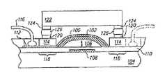
먼저, 도 1을 참조하여 대한민국 공개특허공보 제 특2001-0053615호에 개시된 "마이크로 일렉트로닉 기계(MEMS)에 밀봉 덮개가 실링된 장치의 구성"을 상세하게 설명한다.First, with reference to FIG. 1 will be described in detail "constitution of the device is sealed in a microelectronic machine (MEMS) disclosed in the Republic of Korea Patent Publication No. 2001-0053615.
여기서, 도 1은 투명 덮개가 밀봉 실링되는 실리콘 반도체 디바이스의 대표 단면도를 도시한 것으로서, 반도체 기판(104)상에는 금속성의 전도 및 반사 외피 (102)를 포함하는 전도성 리본(100)이 형성되어 있고, 상기 리본(100)은 기판(104) 사이에 공기 간격(106)을 두고 반도체 기판(104)위로 형성되어 있다.1 shows a representative cross-sectional view of a silicon semiconductor device in which a transparent cover is sealed sealed, and a
또한, 기판(104) 표면에는 절연층(110)에 의하여 피복되는 전도성 전극(108)이 형성되어 있고, 상기 전도성 전극(108)은 리본(100)의 아래에 위치되고 또한 공기 간격(106)의 아래에 위치하게 된다.In addition, a
여기서, 반사 외피(102)는 기계적 능동 리본(100)의 지역 위로 연장되고 통상적인 본딩 패드(112) 및 그 말단으로서 구성되고 통상적인 절연 패시베이션 층(114)으로 패시베이션되어 있으며, 상기 패시베이션 층(114)은 본딩 패드들(112)이나 리본 구조들(100/102)을 덮지 않는다.Here, the
또한, 제어와 전력 신호들은 통상적인 와이어 본딩 구조들(116)을 사용하여 반도체 디바이스에 연결된다.In addition, control and power signals are coupled to the semiconductor device using conventional
통상적인 반도체 제조 기술들에 따르면, 디바이스들은 반도체 기판의 표면상에 가능한 한 밀집되어 형성되나, 여기에 있어서는 광학 유리가 반도체 디바이스상에 직접 밀봉 실링되었기 때문에 본딩 패드들(112)은 덮개 실링(sealing) 지역 (118)을 제공하기 위해 리본 구조들(100/102)로부터 상당한 거리만큼 이격되어 형성되어 있고, 납땜 가능 물질(120)이 덮개 실링 지역(118)상에 형성된다.According to conventional semiconductor fabrication techniques, the devices are formed as densely as possible on the surface of the semiconductor substrate, but in this case the
덮개(122)는 양호한 밀봉을 수행하기 위하여 양질의 광학 물질로 형성되는 것이 바람직하고, 원치 않는 방사(radiation), 반사도 강화 또는 반사도 감소 등을 포함하는 다양한 목적을 위하여 사용된다.The
그러나, 상기 덮개(122)는 상술한 바와 같은 목적에 사용되는 것에 한정되는 것이 아니고 다양한 목적을 위하여 광학적으로 민감한 물질에 의해 코팅되어 있을 수 도 있다.However, the
상술한 바와 같이 덮개가 덮개 실링 지역(118) 위를 덮기에 맞는 적당한 크기로 형성되는 경우, 납땜 가능 물질(124)은 통상적인 반도체 가공 기술들을 사용하여 덮개의 한면의 주위를 둘러싸는 링에 형성된 후, 덮개가 반도체 디바이스에 결합될 수 있도록 땜납(126)은 납땜 가능한 물질(124) 위로 증착된다.When the lid is formed of a suitable size to cover over the
여기서, 비록 비율에 맞춰 도시되지는 않았지만, 서로간의 간섭을 방지하기 위해 덮개(122)와 리본 구조들(100/102)은 떨어져서 실장(mount)되고, 이에 의하여 상기 기술된 구조들(100/102)은 상부 또는 하부로 자유롭게 이동한다.Here, although not shown to scale, the
그러나, 이와 같은 종래의 마이크로 일렉트로닉 기계(MEMS)의 밀봉 방법의 경우, 기판과 덮개 사이에 솔더를 삽입한 후 적층하고, 소정의 온도 조건에서 리플로우(reflow) 공정을 통하여 솔더에 열을 인가하여 기판과 덮개를 상호 접합시키기 때문에 작업속도가 느려 생산성이 저하된다는 문제점이 있었다.However, in the sealing method of the conventional microelectronic machine (MEMS), the solder is inserted between the substrate and the lid and then laminated, and heat is applied to the solder through a reflow process at a predetermined temperature condition. Since the substrate and the lid are bonded to each other, there is a problem that productivity is lowered due to a slow working speed.
또한, 기판과 덮개 사이에 개재되는 솔더의 위치 및 도포량에 따라 밀봉이 완전하게 수행되지 못하는 경우에도 솔더를 더 부가하는 등의 리워크(rework) 공정을 수행할 수 없다는 문제점이 또한 있었다.In addition, there is also a problem that a rework process such as adding solder may not be performed even when the sealing is not completely performed according to the position and the application amount of the solder interposed between the substrate and the cover.
상기와 같은 종래 기술에 따른 문제점을 해결하기 위하여 국내 특허출원번호 P2004-035634호에는 "측면 밀봉부재가 형성된 MEMS 패키지 및 그 제조방법"이 개시되어 있다.In order to solve the problems according to the prior art as described above, Korean Patent Application No. P2004-035634 discloses a MEMS package and a method of manufacturing the side sealing member is formed.
도 2는 종래 개선된 기술에 따른 측면 밀봉부재가 형성된 MEMS 패키지의 단면도이다.2 is a cross-sectional view of a MEMS package having a side sealing member according to a conventional improved technique.
종래 개선된 기술에 따른 측면 밀봉부재가 형성된 MEMS 패키지는 베이스 기판상에 형성되는 MEMS(Micro-Electro-Mechanical Devices) 소자를 커버하는 리드 글래스의 측면에 밀봉부재가 형성된 것으로서, 도 3에 도시된 바와 같이, MEMS 소자(300)가 형성된 베이스 기판(100), 페시베이션층(200), 금속층(400), 스페이서(500), 리드 글래스(600) 및 밀봉부재(700)를 포함하여 구성되어 있다.MEMS package having a side sealing member according to the conventional improved technology is a sealing member formed on the side of the lead glass to cover the micro-electro-mechanical devices (MEMS) element formed on the base substrate, as shown in FIG. Similarly, the
여기에서, 스페이서(500)는 MEMS 소자(300)를 둘러싸는 형상으로 패터닝된 금속층(400)에 일측면이 접촉된 상태로 베이스 기판(100)상에 실장되어 있고, 베이스 기판 (100)에 형성된 MEMS 소자(300)가 상하 방향으로 구동할 수 있도록 하는 자유공간을 형성시키는 역할을 수행한다.Here, the
또한, 상기 스페이서(500)는 베이스 기판(100)에 형성되는 MEMS 소자(300)를 커버하는 리드 글래스(600)를 실장시키는 역할을 수행하되, 상기 리드 글래스(600)에 형성된 메탈층(610)을 개재하여 리드 글래스(600)와 정합된다.In addition, the
이때, 상기 스페이서(500)는 메탈, 에폭시, 플라스틱 및 글래스 중 어느 하 나의 재질로 구성되어 있다.In this case, the
리드 글래스(600)는 스페이서(500)에 적층되어 베이스 기판(100)에 형성된 MEMS 소자(300)를 습기 또는 먼지 등의 외부 환경으로부터 보호하는 역할을 수행하는 것으로서, 상기 스페이서(500)와 정합되는 부분에는 소정의 밀봉부재(700)와의 접촉력을 강화시키기 위한 메탈층(610)이 형성되어 있다.The
여기서, 상기 리드 글래스(600)에는 외부로부터 입사되는 입사광의 투과 효율을 높이기 위하여 일면 또는 양면에 AR 코팅이 형성될 수 도 있다.Here, AR coating may be formed on one or both surfaces of the
밀봉부재(700)는 베이스 기판(100)상에 실장되는 MEMS 소자(300)를 외부 환경으로부터 밀봉시키는 역할을 수행하는 것으로서, 베이스 기판(100)에 형성된 금속층(400)과 스페이서(500)에 실장되는 리드 글래스(600)의 메탈층(610) 측면에 형성된다.The sealing
즉, 밀봉부재(700)는 솔더 또는 엑폭시 수지 등의 밀봉용 부재에 대해 프리폼 (preform), 레이저 가공 및 리플로우(reflow) 등의 방법에 의하여 금속층(400)과 리드 글래스(600)의 메탈층(610) 측면에 접착되어 MEMS 소자(300)를 외부 환경으로부터 완전 밀봉(hermic sealing)시킨다.That is, the sealing
이때, 상기 밀봉부재(700)는 외부 환경과의 밀봉을 수행하기 위하여 적어도 10-7mg의 밀봉 레벨을 갖는 것이 바람직 하다.At this time, the sealing
하지만, 종래 개선된 기술에 따른다 할지라도 접착제등이 신뢰성을 보장할 수 없어 완전밀봉이 어렵다는 문제점이 있었다.
However, even if according to the conventional improved technology, there is a problem that the complete seal is difficult because the adhesive or the like cannot guarantee the reliability.
본 발명은 상술한 바와 같은 문제점을 해결하기 위하여, 베이스 기판에 형성된 MEMS 소자를 둘러싸는 리드 글래스의 측면에 금속 밀봉부재를 형성함으로써, 외부 환경으로부터 MEMS 소자를 밀봉처리하는 MEMS 패키지를 제공하는 데 있다.
The present invention is to provide a MEMS package for sealing the MEMS device from the external environment by forming a metal sealing member on the side of the lead glass surrounding the MEMS device formed on the base substrate in order to solve the above problems. .
상기와 같은 목적을 달성하기 위한 본 발명은, MEMS 소자가 실장된 기판; 상기 기판에 접속되어 상기 MEMS 소자를 덮고 있는 덮개; 상기 MEMS 소자를 외부 환경으로부터 밀봉시키기 위하여 상기 기판의 측벽과 덮개의 사이에 형성되어 있는 측벽 밀봉부재; 및 금속성 물질로서 상기 측벽 밀봉부재와 상기 MEMS 소자가 실장된 기판을 완전히 덮고 있는 금속 밀봉부재를 포함하여 이루어진 것을 특징으로 한다.The present invention for achieving the above object is a substrate on which the MEMS device is mounted; A lid connected to the substrate and covering the MEMS element; A sidewall sealing member formed between the sidewall of the substrate and a cover to seal the MEMS device from an external environment; And a metal sealing member completely covering the sidewall sealing member and the substrate on which the MEMS device is mounted as a metallic material.
또한, 본 발명은 MEMS 소자가 실장된 소자 기판; 상기 소자 기판이 실장된 베이스 기판; 상기 소자 기판에 접속되어 상기 MEMS 소자를 덮고 있는 덮개; 상기 MEMS 소자를 외부 환경으로부터 밀봉시키기 위하여 상기 베이스 기판과 상기 소자기판과 덮개로 형성된 구조체의 측벽 사이에 형성되어 있는 측벽 밀봉부재; 및 금속성 물질로서 상기 측벽 밀봉부재와 상기 덮개를 완전히 덮고 있는 금속 밀봉부재를 포함하여 이루어진 것을 특징으로 한다.
In addition, the present invention is a device substrate on which the MEMS device is mounted; A base substrate on which the device substrate is mounted; A cover connected to the device substrate and covering the MEMS device; A sidewall sealing member formed between the base substrate and sidewalls of a structure formed of the device substrate and the cover to seal the MEMS device from an external environment; And a metal sealing member completely covering the sidewall sealing member and the cover as a metallic material.
이하, 첨부 도면을 참조하여 본 발명에 따른 금속 밀봉부재가 형성된 MEMS 패키지에 대하여 상세하게 설명한다.Hereinafter, a MEMS package having a metal sealing member according to the present invention will be described in detail with reference to the accompanying drawings.
도 3a는 본 발명의 제1 실시예에 따른 금속 밀봉부재가 형성된 MEMS 소자 패키지의 단면도이다.3A is a cross-sectional view of a MEMS device package having a metal sealing member according to a first embodiment of the present invention.
도면을 참조하면, 본 발명의 제1 실시예에 따른 금속 밀봉 부재가 형성된 MEMS 패키지는, MEMS 소자(310)가 형성된 베이스 기판(300), 하부 범프(331), 상부 범프(332), 리드 글래스(320), 측면 밀봉부재(351), 금속 밀봉부재(352)를 포함하여 구성되어 있다.Referring to the drawings, the MEMS package formed with a metal sealing member according to the first embodiment of the present invention, the
여기서, 베이스 기판(300)은 MEMS 소자(310)가 형성된 반도체 기판 자체이거나, 또는 MEMS 소자(310)가 실장되어 있는 있는 패키지 모듈이다.Here, the
이때, 상기 MEMS 소자(310)는 광메모리, 광디스플레이, 프린터, 광인터커넥션, 홀로그램 및 표시장치 등의 분야에 사용되는 회절형, 반사형 및 투과형 등의 광변조기, 광소자 또는 디스플레이장치 등을 모두 포함한다.In this case, the
하부 범프(331)는 베이스 기판(300)의 실링 지역(330)상에 형성되어 있다. 또한, 상부 범프(332)은 리드 글래스(320)의 실링 지역(330')에 형성되어 있다.The
리드 글래스(320)는 상기 하부 범프(331)와 상부 범프(332)에 의해 에어 스페이스를 확보하면서 베이스 기판(300)에 접합될 수 있다.The
여기서, 리드 글래스(310)에는 외부로부터 입사되는 입사광의 투과 효율을 높이기 위하여 일면 또는 양면에 AR 코팅이 형성될 수 도 있다.Here, the AR may be formed on one or both surfaces of the
측벽 밀봉부재(351)는 베이스 기판(300)상에 실장되는 MEMS 소자(310)를 외 부 환경으로부터 밀봉시키는 역할을 수행하는 것으로서, 베이스 기판(300)과 리드 글래스(320)의 측면에 형성되며, 금속 밀봉부재(352)가 쉽게 증착될 수 있도록 평평한 벽을 형성한다. 이때, 측벽 밀봉부재(351)은 단단하고 견고하기는 하나 밀봉 측면에서는 신뢰성을 보장하기 어렵다. 따라서, 완전 밀봉을 위하여 측벽 밀봉부재(351)와 베이스 기판(300)을 둘러싸는 금속 밀봉 부재(352)를 여러가지 증착 방법, 일예로 스퍼터링이나 기상 증착 등의 방법을 사용하여 형성한다.The side
도 3b는 본 발명의 제2 실시예에 따른 금속 밀봉부재가 형성된 MEMS 소자 패키지의 단면도이다.3B is a cross-sectional view of a MEMS device package having a metal sealing member according to a second embodiment of the present invention.
도면을 참조하면, 본 발명의 제2 실시예에 따른 금속 밀봉 부재가 형성된 MEMS 패키지는, MEMS 소자(310)가 형성된 베이스 기판(300), 하부 범프(331), 상부 범프(332), 리드 글래스(320), 측면 밀봉부재(351), 금속 밀봉부재(352), 외부 보호층(353)을 구비하고 있다.Referring to the drawings, the MEMS package formed with a metal sealing member according to the second embodiment of the present invention, the
베이스 기판(300)에는 MEMS 소자(310)가 형성되어 있으며, 실링 지역(330)에 하부 범프(331)가 형성되어 있다. 상부 범프(332)는 리드 글래스(320)의 실링 지역(330')에 형성되어 있다.The
리드 글래스(320)는 하부 범프(331)과 상부 범프(332)를 통해 에어 스페이스를 확보하며 베이스 기판(300)에 접합되어 베이스 기판(300)에 형성된 MEMS 소자(310)의 활성 공간을 제공한다.The
측벽 밀봉부재(351)는 베이스 기판(300)상에 실장되는 MEMS 소자(310)를 외부 환경으로부터 밀봉시키는 역할을 수행하는 것으로서, 베이스 기판(300)과 리드 글래스(320)의 측면에 형성되며, 금속 밀봉부재(352)가 쉽게 증착될 수 있도록 평평한 벽을 형성한다. 이때, 측벽 밀봉부재(351)은 단단하고 견고하기는 하나 밀봉 측면에서는 신뢰성을 보장하기 어렵다. 따라서, 완전 밀봉을 위하여 측벽 밀봉부재(351)와 베이스 기판(300)을 둘러싸는 금속 밀봉 부재(352)를 여러가지 증착 방법, 일예로 스퍼터링이나 기상 증착 등의 방법을 사용하여 형성한다.The side
그리고, 본 발명의 제1 실시예와 달리 제2 실시예에서는 외곽의 금속 밀봉 부재(352)를 보호하기 위하여 접착제 등이 도포되어 외부 보호층(353)을 형성한다.Unlike the first embodiment of the present invention, in the second embodiment, an adhesive or the like is applied to protect the outer
도 3c는 본 발명의 제3 실시예에 따른 금속 밀봉부재가 형성된 MEMS 소자 패키지의 단면도이다.3C is a cross-sectional view of a MEMS device package having a metal sealing member according to a third embodiment of the present invention.
도면을 참조하면, 본 발명의 제3 실시예에 따른 금속 밀봉 부재가 형성된 MEMS 패키지는, MEMS 소자(310)가 형성된 베이스 기판(300), 하부 범프(331), 상부 범프(332), 리드 글래스(320), 1차 측면 밀봉부재(351a), 2차 측면 밀봉부재(351b), 1차 금속 밀봉부재(352a), 2차 금속 밀봉부재(352b)을 포함하여 구성되어 있다.Referring to the drawings, the MEMS package formed with a metal sealing member according to the third embodiment of the present invention, the
여기서, 베이스 기판(300)은 MEMS 소자(310)가 형성된 반도체 기판 자체이거나, 또는 MEMS 소자(310)가 실장되어 있는 패키지 모듈이다.Here, the
MEMS 소자(310)는 광메모리, 광디스플레이, 프린터, 광인터커넥션, 홀로그램 및 표시장치 등의 분야에 사용되는 회절형, 반사형 및 투과형 등의 광변조기, 광소자 또는 디스플레이장치 등을 모두 포함한다.The
하부 범프(331)는 베이스 기판(300)의 MEMS 소자의 실링 지역(330)상에 형성 되어 있다. 또한, 상부 범프(333)은 리드 글래스(320)의 실링 지역(330')에 형성되어 있다.The
리드 글래스(320)는 하부 범프(331)와 상부 범프(332)를 이용하여 에어 스페이스를 확보하며 베이스 기판(300)에 접합되어 베이스 기판(300)에 형성된 MEMS 소자(310)의 활성 공간을 제공한다.The
1차 측벽 밀봉부재(351a)는 베이스 기판(300)상에 실장되는 MEMS 소자(310)를 외부 환경으로부터 밀봉시키는 역할을 수행하는 것으로서, 베이스 기판(300)과 리드 글래스(310)의 측면에 형성되며, 1차 금속 밀봉부재(352a)가 쉽게 증착될 수 있도록 평평한 벽을 형성한다. 이때, 1차 측벽 밀봉부재(351a)은 단단하고 견고하기는 하나 밀봉 측면에서는 신뢰성을 보장하기 어렵다. 따라서, 완전 밀봉을 위하여 1차 측벽 밀봉부재(351a)와 베이스 기판(300)을 둘러싸는 1차 금속 밀봉 부재(352a)를 여러가지 증착 방법, 일예로 스퍼터링이나 기상 증착 등의 방법을 사용하여 형성한다.The primary
더 나아가 본 발명의 제1 또는 제 2 실시예와 달리 제3 실시예에서는 측벽 밀봉부재와 금속 밀봉부재를 다층으로 형성한다.Furthermore, unlike the first or second embodiment of the present invention, in the third embodiment, the side wall sealing member and the metal sealing member are formed in multiple layers.
즉, 1차 측벽 밀봉부재(351a) 위에 1차 금속 밀봉 부재(352a)를 형성하고, 1차 금속 밀봉 부재(352a) 위에 접착제 등을 사용하여 2차 측벽 밀봉부재(351b)을 형성한다. 이러한 2차 측벽 밀봉부재(351b)는 1차 금속 밀봉부재(352)를 보호할 뿐만 아니라 2차 금속 밀봉부재(352b)가 쉽게 증착될 수 있도록 한다.That is, the primary
이처럼 2차 측벽 밀봉부재(351b)를 형성한 후에는 2차 금속 밀봉부재(352b) 를 형성하여 완전밀봉을 달성한다.After the secondary
한편, 본 발명의 제1 실시예 내지 제3 실시예에서 MEMS 소자(310)는 광소자인 것에 대하여 주로 설명하였고 따라서 리드 글래스(320)가 필요하였지만 광소자가 아닌 경우에는 일반적인 기판이 리드 글래스 대신 사용될 수 있다.Meanwhile, in the first to third embodiments of the present invention, the
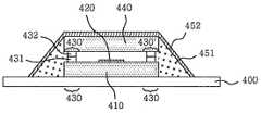
도 4a는 본 발명의 제4 실시예에 따른 금속 밀봉부재가 형성된 MEMS 소자 패키지의 단면도이다.4A is a cross-sectional view of a MEMS device package having a metal sealing member according to a fourth embodiment of the present invention.
도면을 참조하면, 본 발명의 제4 실시예에 따른 금속 밀봉부재가 형성된 MEMS 소자 패키지는, 베이스 기판(400), 소자 기판(410), MEMS 소자(420), 하부 범프(431), 상부 범프(432), 덮개(440), 측벽 밀봉부재(451), 금속 밀봉부재(452)을 구비하고 있다.Referring to the drawings, the MEMS device package formed with a metal sealing member according to the fourth embodiment of the present invention, the
여기서, 베이스 기판(400)은 MEMS 소자(420)가 형성된 소자 기판(410)이 다이 본딩되어 실장되는 매개체로서의 역할을 수행하는 일반적인 인쇄회로기판으로서, 소정의 전기 신호를 외부로 전달하거나 또는 전달받기 위한 와이어(미도시)가 연결되는 패드(pad)(미도시)가 형성되어 있다.Here, the
하부 범프(431)는 소자 기판(410)의 실링 지역(430)상에 형성되어 있다. 또한, 상부 범프(432)은 덮개(440)의 실링 지역(430')에 형성되어 있다.The
소자 기판(410)과 덮개(440)은 하부 범프(431)과 상부 범프(432)에 의해 에어 스페이스를 확보하여 MEMS 소자(420)의 활성 공간을 제공한다.The
측벽 밀봉부재(451)는 베이스 기판(400)상에 실장되는 MEMS 소자(420)의 소자 기판(410)과 덮개(440)의 구조체를 외부 환경으로부터 밀봉시키는 역할을 수행 하는 것으로서, 베이스 기판(400)과 소자 기판(410)과 덮개(440)로 이루어진 구조체의 측벽에 형성된다. 이때, 측벽 밀봉부재(451)는 단단하고 견고하지만 밀봉에 있어서 신뢰성을 보장하기 어렵다.The side
따라서, 베이스 기판(400)의 상면과 측벽 밀봉부재(451)그리고 덮개(440)의 상면을 에워싸는 금속 밀봉부재(452)를 증착하여 완전밀봉을 달성할 수 있다.Therefore, a full seal may be achieved by depositing a
도 4b는 본 발명의 제5 실시예에 따른 금속 밀봉부재가 형성된 MEMS 소자 패키지의 단면도이다.4B is a cross-sectional view of a MEMS device package having a metal sealing member according to a fifth embodiment of the present invention.
도면을 참조하면, 본 발명의 제5 실시예에 따른 금속 밀봉부재가 형성된 MEMS 소자 패키지는, 베이스 기판(400), 소자 기판(410), MEMS 소자(420), 하부 범프(431), 상부 범프(432), 덮개(440), 측벽 밀봉부재(451), 금속 밀봉부재(452), 외부 보호층(453)를 구비하고 있다.Referring to the drawings, the MEMS device package formed with a metal sealing member according to a fifth embodiment of the present invention, the
본 발명의 제5 실시예에 따른 금속 밀봉부재가 형성된 MEMS 패키지가 제4 실시예와 다른점은 금속 밀봉부재(452)를 보호할 접착제등에 의한 외부 보호층(453)이 형성되어 있다는 점이다.The MEMS package in which the metal sealing member according to the fifth embodiment of the present invention is formed is different from the fourth embodiment in that an outer
한편, 제4 실시예와 제5 실시예에서도 제3 실시예와 동일하게 다층으로 금속 밀봉부재를 포함하도록 구현할 수도 있다.
Meanwhile, the fourth embodiment and the fifth embodiment may also be implemented to include a metal sealing member in multiple layers as in the third embodiment.
상기한 바와 같이, 본 발명에 따르면 금속 밀봉부재를 사용하여 완전 실링이 가능하도록 하는 효과가 있다.As described above, according to the present invention, there is an effect of enabling a complete sealing using a metal sealing member.
여기에서, 상술한 본 발명에서는 바람직한 실시예를 참조하여 설명하였지만, 해당 기술분야의 숙련된 당업자는 하기의 특허청구범위에 기재된 본 발명의 사상 및 영역으로부터 벗어나지 않는 범위 내에서 본 발명을 다양하게 수정 및 변경할 수 있음을 이해할 수 있을 것이다.Herein, while the present invention has been described with reference to the preferred embodiments, those skilled in the art will variously modify the present invention without departing from the spirit and scope of the invention as set forth in the claims below. And can be changed.
Claims (6)
Translated fromKoreanPriority Applications (2)
| Application Number | Priority Date | Filing Date | Title |
|---|---|---|---|
| KR1020040080490AKR100855819B1 (en) | 2004-10-08 | 2004-10-08 | MEMS package with metal sealing member |
| US11/180,308US7368816B2 (en) | 2004-10-08 | 2005-07-12 | Micro-electro-mechanical system (MEMS) package having metal sealing member |
Applications Claiming Priority (1)
| Application Number | Priority Date | Filing Date | Title |
|---|---|---|---|
| KR1020040080490AKR100855819B1 (en) | 2004-10-08 | 2004-10-08 | MEMS package with metal sealing member |
Publications (2)
| Publication Number | Publication Date |
|---|---|
| KR20060031451A KR20060031451A (en) | 2006-04-12 |
| KR100855819B1true KR100855819B1 (en) | 2008-09-01 |
Family
ID=36144441
Family Applications (1)
| Application Number | Title | Priority Date | Filing Date |
|---|---|---|---|
| KR1020040080490AExpired - Fee RelatedKR100855819B1 (en) | 2004-10-08 | 2004-10-08 | MEMS package with metal sealing member |
Country Status (2)
| Country | Link |
|---|---|
| US (1) | US7368816B2 (en) |
| KR (1) | KR100855819B1 (en) |
Families Citing this family (20)
| Publication number | Priority date | Publication date | Assignee | Title |
|---|---|---|---|---|
| JP4680763B2 (en)* | 2005-12-16 | 2011-05-11 | 住友電工デバイス・イノベーション株式会社 | Electronic device and semiconductor device |
| US7829438B2 (en) | 2006-10-10 | 2010-11-09 | Tessera, Inc. | Edge connect wafer level stacking |
| US7901989B2 (en) | 2006-10-10 | 2011-03-08 | Tessera, Inc. | Reconstituted wafer level stacking |
| US8513789B2 (en) | 2006-10-10 | 2013-08-20 | Tessera, Inc. | Edge connect wafer level stacking with leads extending along edges |
| US7952195B2 (en) | 2006-12-28 | 2011-05-31 | Tessera, Inc. | Stacked packages with bridging traces |
| JP5572089B2 (en) | 2007-07-27 | 2014-08-13 | テッセラ,インコーポレイテッド | Reconfigured wafer stack packaging with pad extension after application |
| US8551815B2 (en) | 2007-08-03 | 2013-10-08 | Tessera, Inc. | Stack packages using reconstituted wafers |
| US8043895B2 (en) | 2007-08-09 | 2011-10-25 | Tessera, Inc. | Method of fabricating stacked assembly including plurality of stacked microelectronic elements |
| WO2009038686A2 (en)* | 2007-09-14 | 2009-03-26 | Tessera Technologies Hungary Kft. | Hermetic wafer level cavity package |
| US20090289349A1 (en)* | 2008-05-21 | 2009-11-26 | Spatial Photonics, Inc. | Hermetic sealing of micro devices |
| US7863699B2 (en)* | 2008-05-21 | 2011-01-04 | Triquint Semiconductor, Inc. | Bonded wafer package module |
| JP5639052B2 (en) | 2008-06-16 | 2014-12-10 | テッセラ,インコーポレイテッド | Edge stacking at wafer level |
| DE102008042196A1 (en)* | 2008-09-18 | 2010-03-25 | Robert Bosch Gmbh | Method for producing a microfluidic component and microfluidic component |
| WO2010104610A2 (en) | 2009-03-13 | 2010-09-16 | Tessera Technologies Hungary Kft. | Stacked microelectronic assemblies having vias extending through bond pads |
| US10366883B2 (en) | 2014-07-30 | 2019-07-30 | Hewlett Packard Enterprise Development Lp | Hybrid multilayer device |
| US10658177B2 (en) | 2015-09-03 | 2020-05-19 | Hewlett Packard Enterprise Development Lp | Defect-free heterogeneous substrates |
| US10586847B2 (en) | 2016-01-15 | 2020-03-10 | Hewlett Packard Enterprise Development Lp | Multilayer device |
| US11088244B2 (en) | 2016-03-30 | 2021-08-10 | Hewlett Packard Enterprise Development Lp | Devices having substrates with selective airgap regions |
| US10381801B1 (en) | 2018-04-26 | 2019-08-13 | Hewlett Packard Enterprise Development Lp | Device including structure over airgap |
| CN112158792B (en)* | 2020-09-22 | 2024-07-02 | 浙江大学 | A low stress packaging structure suitable for MEMS acceleration sensor chip |
Citations (1)
| Publication number | Priority date | Publication date | Assignee | Title |
|---|---|---|---|---|
| JPS60262141A (en)* | 1984-06-08 | 1985-12-25 | Matsushita Electric Ind Co Ltd | electrochromic display element |
Family Cites Families (9)
| Publication number | Priority date | Publication date | Assignee | Title |
|---|---|---|---|---|
| US5837562A (en)* | 1995-07-07 | 1998-11-17 | The Charles Stark Draper Laboratory, Inc. | Process for bonding a shell to a substrate for packaging a semiconductor |
| US5801074A (en)* | 1996-02-20 | 1998-09-01 | Kim; Jong Tae | Method of making an air tight cavity in an assembly package |
| JP3514361B2 (en)* | 1998-02-27 | 2004-03-31 | Tdk株式会社 | Chip element and method of manufacturing chip element |
| US6303986B1 (en) | 1998-07-29 | 2001-10-16 | Silicon Light Machines | Method of and apparatus for sealing an hermetic lid to a semiconductor die |
| US6441481B1 (en)* | 2000-04-10 | 2002-08-27 | Analog Devices, Inc. | Hermetically sealed microstructure package |
| US7166911B2 (en)* | 2002-09-04 | 2007-01-23 | Analog Devices, Inc. | Packaged microchip with premolded-type package |
| DE10253163B4 (en)* | 2002-11-14 | 2015-07-23 | Epcos Ag | Hermetic encapsulation device and wafer scale manufacturing method |
| KR100733242B1 (en)* | 2004-05-19 | 2007-06-27 | 삼성전기주식회사 | MEMs package having side sealing member and manufacturing method thereof |
| US7145213B1 (en)* | 2004-05-24 | 2006-12-05 | The United States Of America As Represented By The Secretary Of The Air Force | MEMS RF switch integrated process |
- 2004
- 2004-10-08KRKR1020040080490Apatent/KR100855819B1/ennot_activeExpired - Fee Related
- 2005
- 2005-07-12USUS11/180,308patent/US7368816B2/ennot_activeExpired - Fee Related
Patent Citations (1)
| Publication number | Priority date | Publication date | Assignee | Title |
|---|---|---|---|---|
| JPS60262141A (en)* | 1984-06-08 | 1985-12-25 | Matsushita Electric Ind Co Ltd | electrochromic display element |
Also Published As
| Publication number | Publication date |
|---|---|
| US20060076670A1 (en) | 2006-04-13 |
| KR20060031451A (en) | 2006-04-12 |
| US7368816B2 (en) | 2008-05-06 |
Similar Documents
| Publication | Publication Date | Title |
|---|---|---|
| KR100855819B1 (en) | MEMS package with metal sealing member | |
| KR100733242B1 (en) | MEMs package having side sealing member and manufacturing method thereof | |
| JP4205110B2 (en) | Optical modulator module package using flip-chip mounting method | |
| US20070092179A1 (en) | MEMS module package | |
| KR101048085B1 (en) | Functional device package and manufacturing method thereof | |
| US20070075417A1 (en) | MEMS module package using sealing cap having heat releasing capability and manufacturing method thereof | |
| KR100584972B1 (en) | MEMS package having a spacer for sealing and manufacturing method thereof | |
| JP2008141208A (en) | Semiconductor package and packaging method using flip-chip bonding technology | |
| KR100883607B1 (en) | MEMS package and its manufacturing method | |
| US7443024B2 (en) | Micro-electro-mechanical system (MEMS) package having side double-sealing member and method of manufacturing the same | |
| KR100815358B1 (en) | Light modulator package with beveled light transmissive cover | |
| KR100872114B1 (en) | MEMS module package and packaging method | |
| KR100704370B1 (en) | Optical modulator module package using sealing cap and manufacturing method thereof | |
| KR100799614B1 (en) | MEMS module package with heat dissipation | |
| KR100857167B1 (en) | Light modulator substrate and light modulator module using it | |
| KR100857172B1 (en) | Mems module package | |
| KR20070038398A (en) | MEMS module package and sealing method using sealing cap with heat dissipation function | |
| KR20070040471A (en) | MEMS device package and packaging method |
Legal Events
| Date | Code | Title | Description |
|---|---|---|---|
| PA0109 | Patent application | St.27 status event code:A-0-1-A10-A12-nap-PA0109 | |
| R18-X000 | Changes to party contact information recorded | St.27 status event code:A-3-3-R10-R18-oth-X000 | |
| PG1501 | Laying open of application | St.27 status event code:A-1-1-Q10-Q12-nap-PG1501 | |
| A201 | Request for examination | ||
| PA0201 | Request for examination | St.27 status event code:A-1-2-D10-D11-exm-PA0201 | |
| R18-X000 | Changes to party contact information recorded | St.27 status event code:A-3-3-R10-R18-oth-X000 | |
| E902 | Notification of reason for refusal | ||
| PE0902 | Notice of grounds for rejection | St.27 status event code:A-1-2-D10-D21-exm-PE0902 | |
| P11-X000 | Amendment of application requested | St.27 status event code:A-2-2-P10-P11-nap-X000 | |
| P13-X000 | Application amended | St.27 status event code:A-2-2-P10-P13-nap-X000 | |
| E701 | Decision to grant or registration of patent right | ||
| PE0701 | Decision of registration | St.27 status event code:A-1-2-D10-D22-exm-PE0701 | |
| GRNT | Written decision to grant | ||
| PR0701 | Registration of establishment | St.27 status event code:A-2-4-F10-F11-exm-PR0701 | |
| PR1002 | Payment of registration fee | St.27 status event code:A-2-2-U10-U11-oth-PR1002 Fee payment year number:1 | |
| PG1601 | Publication of registration | St.27 status event code:A-4-4-Q10-Q13-nap-PG1601 | |
| LAPS | Lapse due to unpaid annual fee | ||
| PC1903 | Unpaid annual fee | St.27 status event code:A-4-4-U10-U13-oth-PC1903 Not in force date:20110827 Payment event data comment text:Termination Category : DEFAULT_OF_REGISTRATION_FEE | |
| PC1903 | Unpaid annual fee | St.27 status event code:N-4-6-H10-H13-oth-PC1903 Ip right cessation event data comment text:Termination Category : DEFAULT_OF_REGISTRATION_FEE Not in force date:20110827 | |
| R18-X000 | Changes to party contact information recorded | St.27 status event code:A-5-5-R10-R18-oth-X000 | |
| R18-X000 | Changes to party contact information recorded | St.27 status event code:A-5-5-R10-R18-oth-X000 |