KR100854834B1 - Method and apparatus for processing thin metal layers - Google Patents
Method and apparatus for processing thin metal layersDownload PDFInfo
- Publication number
- KR100854834B1 KR100854834B1KR1020027007324AKR20027007324AKR100854834B1KR 100854834 B1KR100854834 B1KR 100854834B1KR 1020027007324 AKR1020027007324 AKR 1020027007324AKR 20027007324 AKR20027007324 AKR 20027007324AKR 100854834 B1KR100854834 B1KR 100854834B1
- Authority
- KR
- South Korea
- Prior art keywords
- metal layer
- region
- irradiation
- adjacent
- irradiation beam
- Prior art date
- Legal status (The legal status is an assumption and is not a legal conclusion. Google has not performed a legal analysis and makes no representation as to the accuracy of the status listed.)
- Expired - Fee Related
Links
Images


Classifications
- H—ELECTRICITY
- H01—ELECTRIC ELEMENTS
- H01L—SEMICONDUCTOR DEVICES NOT COVERED BY CLASS H10
- H01L21/00—Processes or apparatus adapted for the manufacture or treatment of semiconductor or solid state devices or of parts thereof
- H01L21/70—Manufacture or treatment of devices consisting of a plurality of solid state components formed in or on a common substrate or of parts thereof; Manufacture of integrated circuit devices or of parts thereof
- H01L21/71—Manufacture of specific parts of devices defined in group H01L21/70
- H01L21/768—Applying interconnections to be used for carrying current between separate components within a device comprising conductors and dielectrics
- H01L21/76838—Applying interconnections to be used for carrying current between separate components within a device comprising conductors and dielectrics characterised by the formation and the after-treatment of the conductors
- H01L21/76886—Modifying permanently or temporarily the pattern or the conductivity of conductive members, e.g. formation of alloys, reduction of contact resistances
- H01L21/76892—Modifying permanently or temporarily the pattern or the conductivity of conductive members, e.g. formation of alloys, reduction of contact resistances modifying the pattern
- H01L21/76894—Modifying permanently or temporarily the pattern or the conductivity of conductive members, e.g. formation of alloys, reduction of contact resistances modifying the pattern using a laser, e.g. laser cutting, laser direct writing, laser repair
- H—ELECTRICITY
- H10—SEMICONDUCTOR DEVICES; ELECTRIC SOLID-STATE DEVICES NOT OTHERWISE PROVIDED FOR
- H10D—INORGANIC ELECTRIC SEMICONDUCTOR DEVICES
- H10D1/00—Resistors, capacitors or inductors
- H10D1/60—Capacitors
- H10D1/68—Capacitors having no potential barriers
- H10D1/692—Electrodes
- Y—GENERAL TAGGING OF NEW TECHNOLOGICAL DEVELOPMENTS; GENERAL TAGGING OF CROSS-SECTIONAL TECHNOLOGIES SPANNING OVER SEVERAL SECTIONS OF THE IPC; TECHNICAL SUBJECTS COVERED BY FORMER USPC CROSS-REFERENCE ART COLLECTIONS [XRACs] AND DIGESTS
- Y10—TECHNICAL SUBJECTS COVERED BY FORMER USPC
- Y10S—TECHNICAL SUBJECTS COVERED BY FORMER USPC CROSS-REFERENCE ART COLLECTIONS [XRACs] AND DIGESTS
- Y10S438/00—Semiconductor device manufacturing: process
- Y10S438/94—Laser ablative material removal
- Y—GENERAL TAGGING OF NEW TECHNOLOGICAL DEVELOPMENTS; GENERAL TAGGING OF CROSS-SECTIONAL TECHNOLOGIES SPANNING OVER SEVERAL SECTIONS OF THE IPC; TECHNICAL SUBJECTS COVERED BY FORMER USPC CROSS-REFERENCE ART COLLECTIONS [XRACs] AND DIGESTS
- Y10—TECHNICAL SUBJECTS COVERED BY FORMER USPC
- Y10S—TECHNICAL SUBJECTS COVERED BY FORMER USPC CROSS-REFERENCE ART COLLECTIONS [XRACs] AND DIGESTS
- Y10S438/00—Semiconductor device manufacturing: process
- Y10S438/955—Melt-back
Landscapes
- Engineering & Computer Science (AREA)
- Physics & Mathematics (AREA)
- Microelectronics & Electronic Packaging (AREA)
- General Physics & Mathematics (AREA)
- Manufacturing & Machinery (AREA)
- Computer Hardware Design (AREA)
- Condensed Matter Physics & Semiconductors (AREA)
- Power Engineering (AREA)
- Optics & Photonics (AREA)
- Laser Beam Processing (AREA)
- Electrodes Of Semiconductors (AREA)
- Recrystallisation Techniques (AREA)
- Internal Circuitry In Semiconductor Integrated Circuit Devices (AREA)
Abstract
Translated fromKorean
Description
Translated fromKorean우선권 주장Priority claim
본원은 2000년 10월 10일자로 출원된 발명의 명칭이 "금속 필름의 측방향 응고를 제공하는 공정 및 시스템(Process and System for Providing Lateral Solidification of Metallic Films"인 제임스 에스. 임의 가출원 제60/239,194호에 기초하여 우선권을 주장하고 있다.This application, filed Oct. 10, 2000, is entitled James S. Arbitrary Provisional Application No. 60 / 239,194, entitled "Process and System for Providing Lateral Solidification of Metallic Films." It claims priority based on the issue.
정부 권리의 고시Notice of Government Rights
본원에 청구된 발명은 계약서 제N66001-98-01-8913호 하에서 미국 국방성 연구 계획국(United States Defense Research Project Agency)으로부터의 기금 투자(funding)로 이루어 이루어졌다. 따라서, 미국 정부는 본 발명에 대한 소정 권리를 갖는다.The invention claimed herein consists of funding from the United States Defense Research Project Agency under contract no.6666-98-01-8913. Thus, the US government has certain rights in the invention.
발명의 분야Field of invention
본 발명은 기판 상에 얇은 금속층을 가공하는 방법 및 장치에 관한 것으로, 특히 금속층의 재응고 영역에서 입형 및 입경(shape and size of grain)과, 입계(grain boundary)의 위치 및 배향을 제어하기 위해 금속층의 하나 이상의 영역을 소정 강도 패턴을 갖는 펄스형 조사(pulsed irradiation)에 의해 용융시키고 재 응고시키는 방법 및 장치에 관한 것이다.The present invention relates to a method and apparatus for processing a thin metal layer on a substrate, in particular to control the shape and size of grain and the position and orientation of grain boundaries in the resolidification region of the metal layer. A method and apparatus for melting and resolidifying one or more regions of a metal layer by pulsed irradiation with a predetermined intensity pattern.
배경 정보Background Information
반도체 소자 가공의 분야에서, 내부의 금속 상호 연결 라인(metal interconnect line)을 포함한 집적 회로 소자의 주요 부분(feature)의 크기를 감소시키려는 경향이 있어 왔다. 이러한 주요 부분의 크기 감소로 인해, 집적 회로 소자의 금속 상호 연결 라인은 작은 단면적을 갖고, 그에 따라 높은 전류 밀도를 보유한다. 이러한 높은 전류 밀도의 보유는 이러한 상호 연결 라인에서의 전자 이동(electromigration)의 발생을 증가시킨다. 결국, 전자 이동은 이러한 소자의 주요 부분의 크기가 작아짐에 따라 집적 회로 소자에서 점점 흔한 불량 기구(failure mechanism)가 되어 가고 있다.In the field of semiconductor device processing, there has been a tendency to reduce the size of major features of integrated circuit devices, including internal metal interconnect lines. Due to the size reduction of this major part, the metal interconnect lines of the integrated circuit device have a small cross-sectional area and thus high current density. This high current density retention increases the occurrence of electron migration in these interconnect lines. As a result, electron transfer is becoming an increasingly common failure mechanism in integrated circuit devices as the size of the major parts of these devices become smaller.
전자 이동은 내부의 금속 이온으로 상호 연결 라인에서 흐르는 전자로부터의 모멘텀을 전달함으로써 유발되는 금속 상호 연결 라인에서의 금속 재료의 수송으로서 관찰된다. 전자 이동은 금속 재료의 수송이 상호 연결 라인에서 보이드(void) 또는 브레이크(break)를 발생시킬 때에 금속층 상호 연결 라인의 불량을 일으킬 수 있다. 또한, 전자 이동은 금속층 상호 연결 라인에서의 이동된 금속 재료가 인접한 상호 연결 라인과 바람직하지 못한 전기 접촉을 이룰 정도로 충분히 큰 벌지부(bulge)를 형성하도록 누적될 수 있다. 이들 불량은 전자 수송이 상호 연결 라인의 금속층의 입계에 평행하게 일어날 때에 가장 자주 발생하는데, 이는 입계가 이동된 금속 이온의 수송을 위한 채널을 제공할 수 있기 때문이다.Electron transport is observed as the transport of metal material in the metal interconnect line caused by transferring momentum from electrons flowing in the interconnect line to the metal ions therein. Electron transfer can cause failure of the metal layer interconnect line when the transport of the metal material causes a void or break in the interconnect line. Electron movement can also accumulate to form a bulge large enough to cause the moved metal material in the metal layer interconnect line to make undesirable electrical contact with an adjacent interconnect line. These defects most often occur when electron transport occurs parallel to the grain boundaries of the metal layer of the interconnect line, since the grain boundaries can provide a channel for the transport of transported metal ions.
전자 이동에 의해 유발되는 금속층 상호 연결 라인에서의 불량 문제는 금속층 상호 연결 라인에서의 전자 수송의 방향을 따른 총 입계 밀도를 감소시키도록 금속층 상호 연결 라인에서의 입경을 증가시킴으로써 그리고 전자 수송의 방향에 대해 큰 각도(이상적으로 90°)를 형성하도록 입계의 배향을 제어함으로써 완화될 수도 있다.The problem of defects in metal layer interconnect lines caused by electron transfer is caused by increasing the particle diameter in the metal layer interconnect lines and decreasing the direction of electron transport to reduce the total grain boundary density along the direction of electron transport in the metal layer interconnect lines. It may be relaxed by controlling the orientation of the grain boundaries to form a large angle (ideally 90 °) with respect to.
집적 회로 소자의 금속층 상호 연결 라인에서의 전자 이동의 문제를 완화시킬 뿐만 아니라, 높은 컨덕턴스 및 큰 기계 강도를 갖는 얇은 금속층에 대해 다른 분야에서 일반적인 요구가 있는데, 이는 금속층에서 입경을 증가시킴으로써 그리고 입계의 위치 및 배향을 제어함으로써 얻어질 수 있다. 따라서, 집적 회로 소자의 금속층 상호 연결 라인을 포함한 금속층에서의 입경 및 입상과, 입계의 위치 및 배향을 제어하는 방법 및 장치에 대한 필요성이 명백하게 존재한다.In addition to mitigating the problem of electron transfer in the metal layer interconnect lines of integrated circuit devices, there is a general need in other fields for thin metal layers with high conductance and large mechanical strength, which is due to increasing the grain size in the metal layer and It can be obtained by controlling the position and orientation. Thus, there is a clear need for a particle diameter and granularity in a metal layer, including a metal layer interconnection line of an integrated circuit device, and a method and apparatus for controlling the position and orientation of grain boundaries.
발명의 요약Summary of the Invention
본 발명에 따르면, 조사 강도가 없는 적어도 하나의 "섀도우 영역(shadow region)"과 완전한 조사 강도를 갖는 적어도 하나의 "빔릿(beamlet)"을 구비한 강도 패턴을 갖는 제1 조사 빔 펄스(예컨대, 엑시머 레이저 빔 펄스)로 금속층을 조사하는 단계를 포함하는, 기판 상에 배치된 금속층을 가공하는 방법이 제공된다. 빔릿의 강도는 빔릿에 의해 중첩되는 금속층의 각각의 영역은 전체 두께에 걸쳐 용융되고 섀도우 영역에 의해 중첩되는 금속층의 각각의 영역은 적어도 부분적인 미용융 상태로 남도록 구성된다. 각각의 용융 영역은 적어도 하나의 인접한 적어도 부분적인 미용융 영역에 인접한다.According to the present invention, a first irradiation beam pulse (eg, having an intensity pattern with at least one “shadow region” without irradiation intensity and at least one “beamlet” with complete irradiation intensity (eg, A method of processing a metal layer disposed on a substrate is provided, the method comprising irradiating the metal layer with an excimer laser beam pulse). The intensity of the beamlet is configured such that each region of the metal layer overlapped by the beamlet melts over the entire thickness and each region of the metal layer overlapped by the shadow region remains at least partially unmelted. Each melt region is adjacent to at least one adjacent at least partial unmelted region.
제1 조사 빔 펄스에 의한 조사 후, 금속층의 각각의 용융 영역은 냉각되어 재응고된다. 각각의 용융 영역의 재응고 중, 맞닿은 결정립이 특성 성장 거리만큼 성장한 후에 성장하는 결정립이 동일한 용융 영역에서 성장하는 다른 결정립에 맞닿을(충돌할) 때까지 결정립이 각각의 인접한 적어도 부분적인 미용융 영역으로부터 내부에서 성장한다. 그 후, 제1 조사 빔 펄스는 추가 가공을 위한 이전 조사 빔 펄스가 되고, 금속층은 이전 조사 빔 펄스와 동일한 강도 패턴을 갖지만 적어도 하나의 빔릿과 적어도 하나의 섀도우 영역이 이전 조사 빔 펄스에 의한 조사 후의 재응고 중에 성장하는 결정립의 특성 성장 거리보다 작은 거리만큼 금속층에 대해 이동된 상태의 추가 조사 빔 펄스에 의해 조사된다. 금속층이 추가 조사 빔 펄스에 의해 조사될 때, 이동된 빔릿에 의해 중첩되는 금속층의 각각의 영역은 전체 두께에 걸쳐 용융되고, 이동된 섀도우 영역에 의해 중첩되는 금속층의 각각의 영역은 적어도 부분적인 미용융 상태로 남는다. 각각의 용융 영역은 적어도 하나의 인접한 적어도 부분적인 미용융 영역에 인접한다.After irradiation with the first irradiation beam pulse, each molten region of the metal layer is cooled and resolidified. During resolidification of each molten region, after the contacting grains have grown by a characteristic growth distance, the grains are in each adjacent at least partial unmelted region until the growing grains abut (collide) with other grains growing in the same melt region. From inside grows. Then, the first irradiation beam pulse becomes a previous irradiation beam pulse for further processing, and the metal layer has the same intensity pattern as the previous irradiation beam pulse, but at least one beamlet and at least one shadow area are irradiated by the previous irradiation beam pulse. During subsequent resolidification, it is irradiated by a further irradiation beam pulse that is moved relative to the metal layer by a distance smaller than the characteristic growth distance of the grains growing. When the metal layer is irradiated by a further irradiation beam pulse, each area of the metal layer overlapped by the moved beamlet melts over the entire thickness, and each area of the metal layer overlapped by the moved shadow area is at least partially cosmetic. Remain fused. Each melt region is adjacent to at least one adjacent at least partial unmelted region.
추가 조사 빔 펄스에 의한 조사 후, 금속층의 각각의 용융 영역은 냉각되어 재응고된다. 각각의 용융 영역의 재응고 중, 맞닿은 결정립이 맞닿음 결정립 성장 거리만큼 성장한 후에 성장하는 결정립이 동일한 용융 영역에서 성장하는 다른 결정립에 맞닿을 때까지 결정립이 각각의 인접한 적어도 부분적인 미용융 영역으로부터 내부에서 성장한다. 그 후, 추가 빔 펄스는 추가 가공을 위한 이전 조사 빔 펄스가 되고, (1) 이전 조사 빔 펄스와 동일한 강도 패턴을 갖지만 적어도 하나의 빔 릿과 적어도 하나의 섀도우 영역이 특성 성장 거리보다 작은 거리만큼 금속층에 대해 추가로 이동된 상태의 추가 조사 빔 펄스로의 금속층의 조사 단계와, (2) 추가 조사 빔 펄스에 의한 조사 후의 금속층의 각각의 용융 영역의 재응고 단계가 원하는 결정립 구조가 금속층에서 얻어질 때까지 필요에 따라 반복된다.After irradiation with the additional irradiation beam pulses, each melt region of the metal layer is cooled and resolidified. During resolidification of each melt region, the grains are internal from each adjacent at least partially unmelted region until the abutting grains grow by the abutting grain growth distance until the growing grains meet other grains growing in the same melt region. Grow in. The additional beam pulse then becomes the previous irradiation beam pulse for further processing, and (1) has the same intensity pattern as the previous irradiation beam pulse, but at a distance such that at least one beamlet and at least one shadow area are less than the characteristic growth distance. Irradiation of the metal layer with the additional radiation beam pulses further moved relative to the metal layer, and (2) recrystallization of each molten region of the metal layer after the irradiation with the additional radiation beam pulses, the desired grain structure is obtained in the metal layer. Repeat as necessary until the loss.
조사 빔 펄스는 레이저 빔 펄스, 전자 빔 펄스, 이온 빔 펄스 또는 다른 조사 빔 펄스일 수도 있다. 조사 빔 펄스의 강도 패턴은 조사 빔 펄스가 통과하는 마스크에 의해 한정되고, 금속층에 대한 강도 패턴의 이동은 금속층을 갖는 기판을 이동시키거나 마스크를 이동시킴으로써 달성될 수도 있다.The irradiation beam pulse may be a laser beam pulse, an electron beam pulse, an ion beam pulse or another irradiation beam pulse. The intensity pattern of the irradiation beam pulse is defined by the mask through which the irradiation beam pulse passes, and the movement of the intensity pattern with respect to the metal layer may be accomplished by moving the substrate or moving the mask with the metal layer.
본 발명의 방법의 제1 예시 실시예에 따르면, 금속층은 각각의 소정 형상을 갖는 하나 이상의 금속층 스트립으로 미리 패터닝되고, 제1 조사 빔 펄스의 강도 패턴은 다중이고 규칙적으로 이격되며 비교적 작은 도트형 섀도우 영역의 하나 이상의 시리즈(series)를 갖고, 섀도우 영역의 각각의 시리즈는 각각의 금속층 스트립의 중심선을 따라 각각의 영역에 중첩한다. 제1 조사 빔 펄스의 강도 패턴은 섀도우 영역에 의해 중첩되지 않는 하나 이상의 금속층 스트립의 모든 영역에 중첩하는 빔릿도 구비한다. 각각의 강도 패턴이 이전 펄스의 강도 패턴과 동일하지만 그에 대해 이동된 상태의 조사 빔 펄스로의 하나 이상의 금속층 스트립의 여러 회의 반복 조사와, 각각의 조사 후의 각각의 용융 영역의 재응고 후, 각각의 금속층 스트립이 입계의 위치에서 금속층 스트립에 대략 직각인 각각의 입계에 의해 분리되는 단일 결정립 영역을 갖는 원하는 결정립 구조가 얻어진다.According to a first exemplary embodiment of the method of the present invention, the metal layers are previously patterned into one or more strips of metal layers each having a predetermined shape, and the intensity patterns of the first irradiation beam pulses are multiple, regularly spaced and relatively small dot shadows. With one or more series of regions, each series of shadow regions overlap each region along the centerline of each metal layer strip. The intensity pattern of the first irradiation beam pulse also includes beamlets that overlap all regions of the one or more strips of metal layer that are not overlapped by the shadow regions. After several repeated irradiations of one or more strips of metal layer into the irradiation beam pulses, with each intensity pattern being the same as the intensity pattern of the previous pulse but shifted against it, and after resolidification of each melt region after each irradiation, The desired grain structure is obtained with a single grain region separated by each grain boundary perpendicular to the metal layer strip at the location of the grain boundaries.
본 발명의 방법의 제2 예시 실시예에 따르면, 금속층은 각각의 소정 형상을 갖는 하나 이상의 금속층 스트립으로 미리 패터닝된다. 제1 조사 빔 펄스의 강도 패턴은 각각의 금속층 스트립의 중심선에 중첩하는 하나 이상의 비교적 협소한 스트립형 섀도우 영역과, 이 섀도우 영역에 의해 중첩되지 않는 하나 이상의 금속층 스트립의 모든 영역에 중첩하는 빔릿을 갖는다. 제1 조사 빔 펄스의 강도 패턴과 동일한 강도 패턴을 갖지만 이전 펄스의 강도 패턴에 대해 이동된 상태의 조사 빔 펄스에 의한 하나 이상의 금속층 스트립의 여러 회의 반복 조사와, 각각의 조사 후의 각각의 용융 영역의 재응고 후, 각각의 금속층 스트립의 결정립 구조는 입계의 각각의 위치에서 금속층 스트립에 대해 큰 각도를 형성하는 입계를 구비한 비교적 큰 결정립을 포함한다.According to a second exemplary embodiment of the method of the present invention, the metal layers are previously patterned into one or more strips of metal layers each having a predetermined shape. The intensity pattern of the first irradiation beam pulse has one or more relatively narrow strip-shaped shadow regions overlapping the centerline of each metal layer strip, and beamlets overlapping all regions of the at least one metal layer strip that are not overlapped by the shadow regions. . Several repetitive irradiations of one or more strips of metal layer by the irradiation beam pulses having the same intensity pattern as the intensity pattern of the first irradiation beam pulse but shifted with respect to the intensity pattern of the previous pulse, and of each molten region after each irradiation. After resolidification, the grain structure of each metal layer strip includes relatively large grains with grain boundaries that form a large angle with respect to the metal layer strip at each position of the grain boundaries.
본 발명의 방법의 제3 예시 실시예에 따르면, 금속층은 규칙적으로 이격되고 상호 직각인 대각선의 각각의 교차부에 배치된 다중이고 비교적 작은 도트형 섀도우 영역과, 이 섀도우 영역에 의해 중첩되지 않는 금속층의 모든 영역에 중첩하는 빔릿의 배열을 구비한 강도 패턴을 갖는 제1 조사 빔 펄스에 의해 조사된다. 빔릿에 의해 중첩되는 금속층의 각각의 영역은 전체 두께에 걸쳐 용융되는 반면에, 섀도우 영역들 중 하나에 의해 중첩되는 금속층의 각각의 영역은 적어도 부분적인 미용융 상태로 남는다. 각각의 용융 영역은 각각의 인접한 용융 영역에 인접한다. 제1 조사 빔 펄스에 의한 조사 후, 각각의 용융 영역은 냉각되어 재응고된다. 각각의 용융 영역의 재응고 중, 결정립이 각각의 인접한 용융 영역에서 각각의 적어도 부분적인 미용융 영역으로부터 성장한다. 섀도우 영역의 간격에 의해 결정된 바와 같은 적어도 부분적인 미용융 영역의 간격은 맞닿은 결정립이 맞닿음 결정립 성장 거리만큼 성장한 후에 각각의 적어도 부분적인 미용융 영역으로부터 성장하는 결정립이 이웃한 적어도 부분적인 미용융 영역으로부터 성장하는 결정립에 맞닿도록 구성된다. 이전 펄스의 강도 패턴과 동일한 강도 패턴을 갖지만 그에 대해 이동된 상태의 조사 빔 펄스에 의한 여러 회의 반복 조사와, 각각의 조사 후의 각각의 용융 영역의 재응고 후, 금속층의 결정립 구조는 대각선 방향의 입계를 구비한 대체로 사각형의 단일 결정립 영역을 포함한다.According to a third exemplary embodiment of the method of the invention, the metal layer is a multiple, relatively small dot-shaped shadow region disposed at each intersection of regularly spaced and mutually perpendicular diagonals, and a metal layer not overlapped by the shadow region. It is irradiated by a first irradiation beam pulse having an intensity pattern with an array of beamlets that overlaps all regions of. Each region of the metal layer overlapped by the beamlet melts over the entire thickness, while each region of the metal layer overlapped by one of the shadow regions remains at least partially unmelted. Each melt zone is adjacent to each adjacent melt zone. After irradiation with the first irradiation beam pulse, each melt region is cooled and resolidified. During resolidification of each melt zone, grains grow from each at least partial unmelted zone in each adjacent melt zone. The spacing of the at least partial unmelted regions as determined by the spacing of the shadow regions is at least partially unmelted regions adjacent to the grains growing from each at least partially unmelted region after the abutting grains have grown by the abutting grain growth distance. It is configured to abut the grains growing from. After several repetitive irradiations with irradiation beam pulses having the same intensity pattern as the previous one, but moved relative to it, and after resolidification of each molten region after each irradiation, the grain structure of the metal layer is in the grain boundary in the diagonal direction. It comprises a generally rectangular single grain region with a.
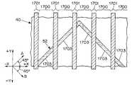
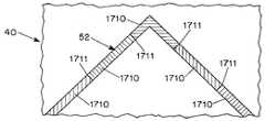
본 발명의 방법의 제4 예시 실시예에 따르면, 각각의 조사 빔의 강도 패턴은 인접한 반복형 셰브런 형상의 규칙적으로 이격된 빔릿을 구비하고, 인접한 반복형 셰브런 형상의 빔릿은 각각의 반복형 셰브런 형상의 빔릿의 피크(peak)가 인접한 반복형 셰브런 형상의 빔릿의 각각의 트로프(trough)와 정렬되고 각각의 반복형 셰브런 형상의 빔릿의 트로프가 인접한 반복형 셰브런 형상의 빔릿의 각각의 피크와 정렬되도록 서로에 대해 엇갈려 있다. 각각의 조사 빔 펄스의 강도 패턴은 각각의 인접한 빔릿들 사이에서 인접하여 위치된 섀도우 영역도 구비한다. 금속층이 이러한 강도 패턴을 갖는 조사 빔 펄스에 의해 조사될 때, 각각의 빔릿에 의해 중첩되는 각각의 영역은 전체 두께에 걸쳐 용융되고, 각각의 섀도우 영역에 의해 중첩되는 각각의 영역은 적어도 부분적인 미용융 상태로 남는다. 각각의 용융 영역은 적어도 부분적인 미용융 모서리와 대향한 반복형 셰브런 형상을 갖는다. 조사 빔 펄스에 의한 조사 후, 각각의 용융 영역은 냉각되어 재응고된다. 각각의 용융 영역의 재응고 중, 맞닿은 결정립이 특성 성장 거리만큼 성장한 후에 대향 모서리로부터 성장하는 결정립이 대략 반복형 셰브런 형상의 용융 영역의 중심선을 따라 서로 맞닿을 때까지 결정립이 용융 영역에서 서로를 향해 대향 방향으로 용융 영역의 각각의 대향 모서리로부터 성장한다. 추가 조사 빔 펄스의 강도 패턴의 빔릿 및 섀도우 영역은 특성 성장 거리보다 작은 거리만큼 반복형 셰브런 형상의 빔릿의 피크의 방향으로 금속층에 대해 이동된다. 다수 회의 조사 및 재응고의 반복 후에 얻어진 결정립 구조는 대체로 육각형 형상을 갖는 인접한 단일 결정립 영역을 갖는다.According to a fourth exemplary embodiment of the method of the present invention, the intensity pattern of each irradiation beam has regularly spaced beamlets of adjacent repeating chevron shapes, and the adjacent repeating chevron shaped beamlets have respective repeating chevron shapes. So that the peaks of the beamlets are aligned with the respective troughs of adjacent repeating chevron shaped beamlets and the troughs of each repeating chevron shaped beamlets are aligned with the respective peaks of the adjacent repeating chevron shaped beamlets. Are staggered against each other. The intensity pattern of each irradiated beam pulse also has a shadow area located adjacent between each adjacent beamlets. When the metal layer is irradiated by irradiation beam pulses having such an intensity pattern, each area overlapped by each beamlet melts over the entire thickness, and each area overlapped by each shadow area is at least partially cosmetic. Remain fused. Each melt region has a repeating chevron shape opposite at least partial unmelted edges. After irradiation with the irradiation beam pulses, each melt region is cooled and resolidified. During the resolidification of each molten region, after the abutting grains grow by a characteristic growth distance, the grains face towards each other in the molten region until the grains growing from the opposite edges contact each other along the centerline of the molten region of approximately repeating chevron shape. It grows from each opposite edge of the melting region in opposite directions. The beamlet and shadow areas of the intensity pattern of the further irradiation beam pulse are moved relative to the metal layer in the direction of the peak of the repeating chevron shaped beamlet by a distance less than the characteristic growth distance. The grain structure obtained after multiple repetitions of irradiation and resolidification has adjacent single grain regions having a generally hexagonal shape.
본 발명의 방법의 제5 예시 실시예에 따르면, 제1 조사 빔의 강도 패턴은 복수개의 규칙적으로 이격되고 비교적 협소한 선형의 스트라이프형 섀도우 영역과, 복수개의 규칙적으로 이격되고 비교적 넓은 선형의 스트라이프형 빔릿을 갖고, 각각의 빔릿은 각각의 인접한 섀도우 영역들 사이에서 인접하여 위치된다. 금속층이 제1 조사 빔 펄스에 의해 조사될 때, 각각의 빔릿에 의해 중첩되는 금속층의 각각의 영역은 전체 두께에 걸쳐 용융되고, 각각의 섀도우 영역에 의해 중첩되는 금속층의 각각의 영역은 적어도 부분적인 미용융 상태로 남는다. 각각의 적어도 부분적인 미용융 영역은 각각의 인접한 용융 영역에 인접한다. 제1 조사 빔 펄스에 의한 조사 후, 금속층의 각각의 용융 영역은 냉각되어 재응고된다. 각각의 용융 영역의 재응고 중, 각각의 결정립은 서로를 향해 대향 방향으로 인접한 적어도 부분적인 미용융 영역으로부터 내부에서 성장하고, 맞닿은 결정립이 제1 맞닿음 결정립 성장 거리만큼 성장한 후에 복수개의 제1 맞닿음 입계의 각각의 입계를 따라 서로 맞닿게 된다. 제1 조사 빔 펄스에 의한 조사에 이은 재응고의 완료 후, 금속층은 제1 조사 빔 펄스의 강도 패턴과 동일한 강도 패턴을 갖지만 섀도우 영역 및 빔릿 이 제1 맞닿음 결정립 성장 거리보다 작은 섀도우 영역의 폭과 적어도 동일한 거리만큼 제1 맞닿음 입계에 직각인 방향으로 이동된 상태의 제2 조사 빔 펄스에 의해 조사된다. 금속층이 제2 조사 빔 펄스에 의해 조사될 때, 각각의 이동된 빔릿에 의해 중첩되는 금속층의 각각의 영역은 전체 두께에 걸쳐 용융되고, 각각의 이동된 섀도우 영역에 의해 중첩되는 금속층의 각각의 영역은 적어도 부분적인 미용융 상태로 남는다. 각각의 적어도 부분적인 미용융 영역은 각각의 인접한 용융 영역에 인접한다. 제2 조사 빔 펄스에 의한 조사 후, 금속층의 각각의 용융 영역은 냉각되어 재응고된다. 각각의 용융 영역의 재응고 중, 각각의 단일 결정립은 서로를 향해 대향 방향으로 인접한 적어도 부분적인 미용융 영역으로부터 내부에서 성장하고, 맞닿은 단일 결정립이 제1 맞닿음 결정립 성장 거리만큼 성장한 후에 복수개의 제2 맞닿음 입계의 각각의 입계를 따라 서로 맞닿게 된다. 제2 조사 빔 펄스에 의한 조사 후의 용융 영역의 재응고의 완료 시, 금속층은 각각의 인접한 제2 맞닿음 입계들 사이에서 연장되는 비교적 긴 단일 결정립을 포함하고 제2 맞닿음 입계에 대략 직각인 측방향 입계를 구비한 결정립 구조를 갖는다.According to a fifth exemplary embodiment of the method of the present invention, the intensity pattern of the first irradiation beam comprises a plurality of regularly spaced and relatively narrow linear striped shadow areas, and a plurality of regularly spaced and relatively wide linear striped shapes. With beamlets, each beamlet is located adjacent between each adjacent shadow regions. When the metal layer is irradiated by the first irradiation beam pulse, each area of the metal layer overlapped by each beamlet is melted over the entire thickness, and each area of the metal layer overlapped by each shadow area is at least partially Remains unmelted. Each at least partial unmelted region is adjacent to each adjacent melt region. After irradiation with the first irradiation beam pulse, each molten region of the metal layer is cooled and resolidified. During resolidification of each melt region, each grain grows internally from at least partially unmelted regions adjacent in opposite directions towards each other, and after the abutted grains have grown by a first contact grain growth distance, a plurality of first fits. Abutting each other along each grain boundary of the grain boundary. After completion of resolidification following irradiation by the first irradiation beam pulse, the metal layer has the same intensity pattern as the intensity pattern of the first irradiation beam pulse, but the width of the shadow region where the shadow region and the beamlet are smaller than the first contact grain growth distance Is irradiated by a second irradiation beam pulse in a state moved in a direction perpendicular to the first contact grain boundary by at least the same distance as. When the metal layer is irradiated by the second irradiation beam pulse, each area of the metal layer overlapped by each moved beamlet is melted over the entire thickness, and each area of the metal layer overlapped by each moved shadow area. Remains at least partially unmelted. Each at least partial unmelted region is adjacent to each adjacent melt region. After irradiation with the second irradiation beam pulse, each of the molten regions of the metal layer is cooled and resolidified. During resolidification of each melt region, each single grain grows internally from at least partially unmelted regions adjacent in opposite directions towards each other, and after abutting single grains have grown by a first contact grain growth distance, 2 abutment Abutting each other along each boundary of the grain boundary. Upon completion of resolidification of the molten region after irradiation by the second irradiation beam pulse, the metal layer comprises a relatively long single grain extending between each adjacent second contact grain boundaries and approximately perpendicular to the second contact grain boundaries. It has a grain structure with an aromatic grain boundary.
본 발명의 방법의 제6 예시 실시예에 따르면, 상기 제5 예시 실시예에서의 제2 조사 빔 펄스에 의한 조사에 이은 금속층의 용융 영역의 재응고의 완료 후, 기판 상의 금속층은 제2 맞닿음 입계에 대해 90°만큼 회전된다. 다음에, 회전된 금속층은 회전된 금속층의 결정립 구조의 제2 맞닿음 입계에 직각인 복수개의 규칙적으로 이격되고 비교적 협소한 선형의 스트라이프형 섀도우 영역과, 역시 제2 맞닿음 입계에 직각인 복수개의 규칙적으로 이격되고 비교적 넓은 선형의 스트라이프형 빔릿을 구비한 강도 패턴을 갖는 제3 조사 빔으로 조사된다. 각각의 빔릿은 각각의 인접한 섀도우 영역들 사이에서 인접하여 위치된다. 회전된 금속층 상의 각각의 지점이 제3 조사 빔 펄스에 의해 조사될 때, 각각의 빔릿에 의해 중첩되는 금속층의 각각의 영역은 전체 두께에 걸쳐 용융되고, 각각의 섀도우 영역에 의해 중첩되는 금속층의 각각의 영역은 적어도 부분적인 미용융 상태로 남는다. 각각의 적어도 부분적인 미용융 영역은 각각의 인접한 용융 영역에 인접한다. 제3 조사 빔 펄스에 의한 조사 후, 금속층의 각각의 용융 영역은 냉각되어 재응고된다. 각각의 용융 영역의 재응고 중, 상이한 단일 결정립이 각각의 적어도 부분적인 미용융 영역으로부터 각각의 인접한 용융 영역 내로 성장하고, 각각의 용융 영역에서 각각의 결정립이 서로를 향해 대향 방향으로 인접한 적어도 부분적인 미용융 영역으로부터 성장하게 하며, 맞닿은 단일 결정립이 제2 맞닿음 결정립 성장 거리만큼 성장한 후에 복수개의 제2 맞닿음 입계의 각각의 입계를 따라 서로 맞닿게 된다. 각각의 맞닿은 단일 결정립은 인접한 제2 맞닿음 입계들 사이의 거리와 동일한 제3 맞닿음 입계를 따라 소정 치수를 갖는다. 제3 조사 빔 펄스에 의한 조사 후에 금속층의 용융 영역의 재응고의 완료 후, 금속층 상의 각각의 지점은 제3 조사 빔 펄스의 강도 패턴과 동일한 강도 패턴을 갖지만 섀도우 영역 및 빔릿이 제2 맞닿음 입계보다 작은 섀도우 영역의 폭과 적어도 동일한 거리만큼 제3 맞닿음 입계에 대략 직각인 방향으로 이동된 상태의 제4 조사 빔 펄스에 의해 조사된다. 금속층 상의 각각의 지점이 제4 조사 빔 펄스에 의해 조사될 때, 각각의 이동된 빔릿에 의해 중첩되는 금속층의 각각의 영역은 전체 두께에 걸쳐 용융되고, 각각의 이동된 섀도우 영역에 의해 중첩되는 금속층의 각각의 영역은 적어도 부분적인 미용융 상태로 남는다. 각각의 적어도 부분적인 미용융 영역은 각각의 인접한 용융 영역에 인접한다. 제4 조사 빔 펄스에 의한 조사 후, 금속층의 각각의 용융 영역은 냉각되어 재응고된다. 각각의 용융 영역의 재응고 중, 각각의 단일 결정립이 각각의 적어도 부분적인 미용융 영역으로부터 각각의 인접한 용융 영역 내로 성장하고, 각각의 용융 영역에서 각각의 단일 결정립이 서로를 향해 대향 방향으로 인접한 적어도 부분적인 미용융 영역으로부터 성장하며, 맞닿은 단일 결정립이 제2 맞닿음 결정립 성장 거리만큼 성장한 후에 복수개의 제4 맞닿음 입계의 각각의 입계를 따라 서로 맞닿게 된다. 제4 조사 빔 펄스에 의한 조사 후에 용융 영역의 재응고의 완료 시, 금속층은 각각의 행 및 열로 대체로 직사각형 형상의 단일 결정립 영역의 배열을 구비하는 결정립 구조를 가지며, 각각의 대체로 직사각형 형상의 단일 결정립 영역은 인접한 제2 맞닿음 입계들 사이의 거리와 동일한 2개의 대향측 상의 소정 치수와, 인접한 제4 맞닿음 입계들 사이의 거리와 동일한 다른 2개의 대향측 상의 소정 치수를 갖는다.According to a sixth exemplary embodiment of the method of the present invention, after completion of resolidification of the molten region of the metal layer following irradiation by the second irradiation beam pulse in the fifth exemplary embodiment, the metal layer on the substrate is in second contact. Rotated by 90 ° with respect to the grain boundaries. Next, the rotated metal layer comprises a plurality of regularly spaced and relatively narrow linear striped shadow areas perpendicular to the second abutment grain boundary of the grain structure of the rotated metal layer, and a plurality of also perpendicular to the second abutment boundary. It is irradiated with a third irradiation beam having an intensity pattern with regularly spaced and relatively wide linear stripe beamlets. Each beamlet is located adjacent between each adjacent shadow areas. When each point on the rotated metal layer is irradiated by the third irradiation beam pulse, each area of the metal layer overlapped by each beamlet is melted over the entire thickness, and each of the metal layers overlapped by each shadow area The region of remains at least partially unmelted. Each at least partial unmelted region is adjacent to each adjacent melt region. After irradiation with the third irradiation beam pulse, each of the molten regions of the metal layer is cooled and resolidified. During resolidification of each melt zone, different single grains grow from each at least partial unmelted zone into each adjacent melt zone, with each grain at least partially adjacent in opposite directions towards each other. The abutment grains are allowed to grow from the unmelted region, and the abutted single grains grow by a second abutment grain growth distance and then abut each other along each grain boundary of the plurality of second abutment grain boundaries. Each abutted single grain has a predetermined dimension along a third abutment grain boundary equal to the distance between adjacent second abutment grain boundaries. After completion of resolidification of the molten region of the metal layer after irradiation by the third irradiation beam pulse, each point on the metal layer has the same intensity pattern as the intensity pattern of the third irradiation beam pulse, but the shadow region and the beamlet are at the second abutment boundary And irradiated by a fourth irradiation beam pulse in a state moved in a direction approximately perpendicular to the third contact grain boundary by at least a distance equal to the width of the smaller shadow area. When each point on the metal layer is irradiated by the fourth irradiation beam pulse, each area of the metal layer overlapped by each moved beamlet is melted over the entire thickness, and the metal layer overlapped by each moved shadow area Each region of the remains at least partially unmelted. Each at least partial unmelted region is adjacent to each adjacent melt region. After irradiation with the fourth irradiation beam pulse, each of the molten regions of the metal layer is cooled and resolidified. During resolidification of each melt region, each single grain grows from each at least partial unmelted region into each adjacent melt region, and in each melt region each single grain is at least adjacent in opposite directions towards each other. Growing from the partial unmelted region, the abutting single grains grow by a second contact grain growth distance and then abut each other along each grain boundary of the plurality of fourth contact grain boundaries. Upon completion of the resolidification of the molten region after irradiation with the fourth irradiation beam pulse, the metal layer has a grain structure having an array of single grain regions having a generally rectangular shape in each row and column, with each generally rectangular shape single grain. The region has a predetermined dimension on two opposing sides equal to the distance between adjacent second abutment grain boundaries and a predetermined dimension on two other opposing sides which is equal to the distance between adjacent fourth abutment grain boundaries.
본 발명의 방법의 제7 예시 실시예에 따르면, 금속층은 소정 형상을 갖는 비교적 협소한 금속 스트립 형태이다. 비교적 협소한 금속 스트립의 폭은 단일 결정립들만 내부에서 성장하도록 충분히 작다. 금속층 스트립은 금속층 스트립을 따라 규칙적인 간격으로 위치된 복수개의 비교적 협소한 선형의 스트라이프형 섀도우 영역과, 각각의 섀도우 영역에 의해 중첩되지 않는 금속층 스트립의 모든 영역에 중첩하는 빔릿을 구비한 강도 패턴을 갖는 제1 조사 빔 펄스에 의해 조사된다. 빔릿에 의해 중첩되는 금속층 스트립의 각각의 영역은 전체 두께에 걸쳐 용융되고, 각 각의 섀도우 영역에 의해 중첩되는 금속층 스트립의 각각의 영역은 적어도 부분적인 미용융 상태로 남는다. 각각의 적어도 부분적인 미용융 영역은 각각의 인접한 용융 영역에 인접한다. 제1 조사 빔 펄스에 의한 조사 후, 금속층 스트립의 각각의 용융 영역은 냉각되어 재응고된다. 각각의 용융 영역의 재응고 중, 상이한 단일 결정립이 각각의 적어도 부분적인 미용융 영역으로부터 각각의 인접한 용융 영역 내로 성장하고, 각각의 용융 영역에서 각각의 단일 결정립이 서로를 향해 대향 방향으로 인접한 적어도 부분적인 미용융 영역으로부터 성장하며, 맞닿은 단일 결정립이 맞닿음 결정립 성장 거리만큼 성장한 후에 복수개의 제1 맞닿음 입계의 각각의 입계를 따라 서로 맞닿게 된다. 제1 조사 빔 펄스에 의한 조사에 이은 각각의 용융 영역의 재응고의 완료 후, 금속 스트립은 제1 조사 빔 펄스와 동일한 강도 패턴을 갖지만 각각의 섀도우 영역 및 빔릿이 맞닿음 결정립 성장 거리보다 작은 섀도우 영역의 폭보다 큰 거리만큼 금속층을 따라 이동된 상태의 제2 조사 빔 펄스로 조사된다. 제2 조사 빔 펄스의 강도 패턴의 빔릿도 금속층에 대해 이동되지만 섀도우 영역에 의해 중첩되지 않는 금속층의 모든 영역에 중첩한다. 금속층 스트립이 제2 조사 빔 펄스에 의해 조사될 때, 이동된 빔릿에 의해 중첩되는 금속층 스트립의 각각의 영역은 전체 두께에 걸쳐 용융되고, 각각의 이동된 섀도우 영역에 의해 중첩되는 금속층 스트립의 각각의 영역은 적어도 부분적인 미용융 상태로 남는다. 각각의 적어도 부분적인 미용융 영역은 각각의 인접한 용융 영역에 인접한다. 제2 조사 빔 펄스에 의한 조사 후, 금속층의 각각의 용융 영역은 냉각되어 재응고된다. 각각의 용융 영역의 재응고 중, 각각의 단일 결정립이 각각의 적어도 부분적인 미용융 영역으로부터 각각의 인접한 용융 영역 내로 성장하고, 각각의 용융 영역에서 각각의 단일 결정립이 서로를 향해 대향 방향으로 인접한 적어도 부분적인 미용융 영역으로부터 성장하며, 맞닿은 단일 결정립이 맞닿음 결정립 성장 거리만큼 성장한 후에 복수개의 제2 맞닿음 입계의 각각의 입계에서 서로 맞닿게 된다. 제2 조사 빔 펄스에 의한 조사에 이은 각각의 용융 영역의 재응고의 완료 후, 금속층 스트립은 각각의 인접한 제2 맞닿음 입계들 사이에서 연장되는 단일 결정립 영역을 구비한 결정립 구조를 갖는다. 각각의 제2 맞닿음 입계는 이 각각의 제2 맞닿음 입계의 위치에서 금속층 스트립에 실질적으로 직각이다.According to a seventh exemplary embodiment of the method of the invention, the metal layer is in the form of a relatively narrow metal strip having a predetermined shape. The width of the relatively narrow metal strip is small enough so that only single grains grow inside. The metal strip has a strength pattern with a plurality of relatively narrow linear striped shadow areas located at regular intervals along the metal layer strip, and beamlets overlapping all areas of the metal layer strip that are not overlapped by each shadow area. Irradiated by the first irradiation beam pulse having. Each region of the metal layer strip overlapped by the beamlets melts over the entire thickness, and each region of the metal layer strip overlapped by each shadow region remains at least partially unmelted. Each at least partial unmelted region is adjacent to each adjacent melt region. After irradiation with the first irradiation beam pulse, each molten region of the metal layer strip is cooled and resolidified. During the resolidification of each melt zone, different single grains grow from each at least partial unmelted zone into each adjacent melt zone, and in each melt zone each at least part adjacent each other in opposite directions towards each other. Growing from the normal unmelted region, the abutting single grains grow by the abutting grain growth distance and then abut each other along each grain boundary of the plurality of first abutment grain boundaries. After completion of resolidification of each molten region following irradiation by the first irradiation beam pulse, the metal strip has the same intensity pattern as the first irradiation beam pulse but with a shadow smaller than the respective grain area and beamlet abutting grain growth distance. The second irradiation beam pulse is irradiated along the metal layer by a distance greater than the width of the region. The beamlets of the intensity pattern of the second irradiation beam pulse also overlap all regions of the metal layer that are moved relative to the metal layer but are not overlapped by the shadow regions. When the metal layer strip is irradiated by the second irradiation beam pulse, each area of the metal layer strip overlapped by the moved beamlets is melted over the entire thickness, and each area of the metal layer strip is overlapped by each moved shadow area. The area remains at least partially unmelted. Each at least partial unmelted region is adjacent to each adjacent melt region. After irradiation with the second irradiation beam pulse, each of the molten regions of the metal layer is cooled and resolidified. During resolidification of each melt region, each single grain grows from each at least partial unmelted region into each adjacent melt region, and in each melt region each single grain is at least adjacent in opposite directions towards each other. Growing from the partial unmelted region, the abutting single grains grow by the abutting grain growth distance and then abut each other at each grain boundary of the plurality of second abutment grain boundaries. After completion of resolidification of each molten region following irradiation by a second radiation beam pulse, the metal layer strip has a grain structure with a single grain region extending between each adjacent second abutment boundaries. Each second abutment boundary is substantially perpendicular to the metal layer strip at the location of each second abutment boundary.
본 발명의 방법의 제8 예시 실시예에 따르면, 적어도 하나의 세그먼트와 맨해튼 형상을 구비한 각각의 소정 형상을 갖는 적어도 하나의 비교적 협소한 금속층 스트립을 포함한다. 각각의 금속층 스트립의 폭은 단일 결정립만 내부에서 성장하도록 충분히 작다. 각각의 금속층 스트립은 복수개의 규칙적으로 이격되고 비교적 협소한 선형의 스트라이프형 섀도우 영역과, 복수개의 규칙적으로 이격되고 비교적 넓은 선형의 스트라이프형 빔릿을 구비한 강도 패턴을 갖는 제1 조사 빔 펄스에 의해 조사된다. 각각의 빔릿은 각각의 인접한 섀도우 영역들 사이에서 인접하여 위치된다. 각각의 금속층 스트립의 각각의 세그먼트는 섀도우 영역 및 빔릿에 대해 대각선으로 배향된다. 각각의 금속층 스트립이 제1 조사 빔 펄스에 의해 조사될 때, 각각의 빔릿에 의해 중첩되는 금속층 스트립의 각각의 영역이 전체 두께에 걸쳐 용융되고, 각각의 섀도우 영역에 의해 중첩되는 적어도 하나의 금속층 스트립의 각각의 영역은 적어도 부분적인 미용융 상태로 남는다. 각각의 적어도 부분적인 미용융 영역은 각각의 인접한 용융 영역에 인접한다. 제1 조사 빔 펄스에 의한 조사에 이어, 각각의 금속층 스트립의 각각의 용융 영역은 냉각되어 재응고된다. 각각의 용융 영역의 재응고 중, 상이한 단일 결정립이 각각의 적어도 부분적인 미용융 영역으로부터 각각의 인접한 용융 영역 내로 성장하고, 각각의 용융 영역에서 각각의 단일 결정립이 서로를 향해 대향 방향으로 인접한 적어도 부분적인 미용융 영역으로부터 성장하며, 맞닿은 단일 결정립이 맞닿음 결정립 성장 거리만큼 성장한 후에 복수개의 제1 맞닿음 입계의 각각의 입계에서 서로 맞닿게 된다. 각각의 제1 맞닿음 입계는 섀도우 영역 및 빔릿에 대략 평행하다. 제1 조사 빔 펄스에 의한 조사에 이은 각각의 금속층 스트립의 각각의 용융 영역의 재응고의 완료 후, 각각의 금속층 스트립은 제1 조사 빔 펄스의 강도 패턴과 동일한 강도 패턴을 갖지만 섀도우 영역 및 빔릿이 이동된 섀도우 영역을 제1 맞닿음 입계에 중첩시키는 거리보다 작은 섀도우 영역의 폭과 적어도 동일한 거리만큼 제1 맞닿음 입계에 직각인 방향으로 이동된 상태의 제2 조사 빔 펄스에 의해 조사된다. 각각의 금속층 스트립이 제2 조사 빔 펄스에 의해 조사될 때, 각각의 이동된 빔릿에 의해 중첩되는 각각의 금속층 스트립의 각각의 영역은 전체 두께에 걸쳐 용융되고, 각각의 이동된 섀도우 영역에 의해 중첩되는 적어도 하나의 금속층 스트립의 각각의 영역은 적어도 부분적인 미용융 상태로 남는다. 각각의 적어도 부분적인 미용융 영역은 각각의 인접한 용융 영역에 인접한다. 제2 조사 빔 펄스에 의한 조사 후, 각각의 금속층 스트립의 각각의 용융 영역은 냉각되어 재응고된다. 각각의 용융 영역의 재응고 중, 각각의 단일 결정립이 각각의 적어도 부분적인 미용융 영역으로부터 각각의 인접한 용융 영역 내로 성장하고, 각각의 용융 영역에서, 각각의 단일 결정립이 서로를 향해 대향 방향으로 인접한 적어도 부분적인 미용융 영역으로부터 성장하며, 맞닿은 단일 결정립이 맞닿음 결정립 성장 거리만큼 성장한 후에 복수개의 제2 맞닿음 입계의 각각의 입계에서 서로 맞닿게 된다. 각각의 제2 맞닿음 입계는 이동된 섀도우 영역 및 이동된 빔릿에 대략 평행하다. 제2 조사 빔 펄스에 의한 조사에 이은 각각의 용융 영역의 재응고의 완료 후, 각각의 금속층 스트립은 각각의 인접한 제2 맞닿음 입계들 사이에서 연장되는 단일 결정립의 영역을 구비한 결정립 구조를 갖는다. 각각의 제2 맞닿음 입계는 제2 맞닿음 입계의 위치에서 각각의 금속층 스트립에 대해 직각으로 배향된다.According to an eighth exemplary embodiment of the method of the invention, it comprises at least one relatively narrow metal layer strip having at least one segment and each predetermined shape having a Manhattan shape. The width of each metal layer strip is small enough so that only a single grain grows inside. Each metal layer strip is irradiated by a first irradiation beam pulse having a plurality of regularly spaced and relatively narrow linear striped shadow areas and an intensity pattern having a plurality of regularly spaced and relatively wide linear striped beamlets. do. Each beamlet is located adjacent between each adjacent shadow areas. Each segment of each metal layer strip is oriented diagonally with respect to the shadow area and the beamlet. When each metal layer strip is irradiated by a first irradiation beam pulse, each region of the metal layer strip overlapped by each beamlet is melted over the entire thickness, and at least one metal layer strip overlapped by each shadow region Each region of the remains at least partially unmelted. Each at least partial unmelted region is adjacent to each adjacent melt region. Subsequent to irradiation by the first irradiation beam pulse, each molten region of each metal layer strip is cooled and resolidified. During the resolidification of each melt zone, different single grains grow from each at least partial unmelted zone into each adjacent melt zone, and in each melt zone each at least part adjacent each other in opposite directions towards each other. Growing from the normal unmelted region, abutting single grains grow by abutment grain growth distances and then abut each other at each grain boundary of the plurality of first abutment grain boundaries. Each first abutment boundary is approximately parallel to the shadow area and the beamlet. After completion of resolidification of each molten region of each metal layer strip following irradiation by the first irradiation beam pulse, each metal layer strip has the same intensity pattern as the intensity pattern of the first irradiation beam pulse, but the shadow region and beamlet And irradiated by a second irradiation beam pulse in a state moved in a direction perpendicular to the first contact grain boundary by a distance at least equal to the width of the shadow region smaller than the distance overlapping the moved shadow region to the first contact grain boundary. When each metal layer strip is irradiated by a second irradiation beam pulse, each area of each metal layer strip overlapped by each moved beamlet is melted over the entire thickness and overlapped by each moved shadow area. Each region of the at least one metal layer strip being left at least partially unmelted. Each at least partial unmelted region is adjacent to each adjacent melt region. After irradiation with the second irradiation beam pulse, each melt region of each metal layer strip is cooled and resolidified. During resolidification of each melt zone, each single grain grows from each at least partially unmelted zone into each adjacent melt zone, and in each melt zone, each single grain lies in opposite directions towards each other. Growing from at least a partial unmelted region, abutting single grains grow by abutting grain growth distances and then abut each other at each grain boundary of the plurality of second abutment grain boundaries. Each second abutment boundary is approximately parallel to the moved shadow area and the moved beamlet. After completion of resolidification of each molten region following irradiation by a second radiation beam pulse, each metal layer strip has a grain structure with regions of single grains extending between each adjacent second abutment boundaries. . Each second abutment grain boundary is oriented at right angles to each metal layer strip at the location of the second abutment grain boundary.
본 발명의 방법의 제9 실시예에 따르면, 금속층은 각각의 소정 형상을 갖는 적어도 하나의 스트라이프 형상의 빔릿을 구비한 강도 패턴을 갖는 제1 조사 빔 펄스에 의해 조사된다. 각각의 빔릿에 의해 중첩되는 금속층의 각각의 영역은 각각의 형상을 갖는 적어도 하나의 스트라이프 형상의 용융 영역을 형성하도록 전체 두께에 걸쳐 용융되고, 각각의 빔릿 영역에 의해 중첩되지 않는 금속층의 각각의 영역은 적어도 부분적인 미용융 상태로 남는다. 각각의 용융 영역은 이 용융 영역의 제1 및 제2 모서리를 따라 적어도 하나의 인접한 적어도 부분적인 미용융 영역에 인접한다. 제1 조사 빔 펄스에 의한 조사 후, 각각의 용융 영역은 냉각되어 재응고된다. 각각의 용융 영역의 재응고 중, 결정립의 제1 및 제2 행은 결정립의 제1 및 제2행이 각각 맞닿음 결정립 성장 거리만큼 성장할 때까지 서로를 향해 대향 방향으로 각각 제1 및 제2 모서리로부터 내부에서 성장한다. 각각의 용융 영역이 각 각의 소정 형상을 갖는 적어도 하나의 재응고 영역을 형성하도록 완전히 재응고된 후, 금속층은 각각의 재응고 영역의 결정립의 제1 및 제2 행 중 하나의 각각의 스트립 형상의 영역으로부터 적어도 하나의 비교적 협소한 금속 스트립을 형성하도록 패터닝된다. 각각의 금속층 스트립은 각각의 소정 형상과, 입계의 위치에서 각각의 금속층 스트립과 비교적 큰 각도를 형성하는 입계에 의해 분리된 단일 결정립의 영역을 갖는다.According to a ninth embodiment of the method of the invention, the metal layer is irradiated by a first irradiation beam pulse having an intensity pattern with at least one stripe shaped beamlet having each predetermined shape. Each region of the metal layer overlapped by each beamlet is melted over the entire thickness to form a molten region of at least one stripe shape having a respective shape, and each region of the metal layer not overlapped by each beamlet region Remains at least partially unmelted. Each melt zone is adjacent to at least one adjacent at least partial unmelted zone along the first and second edges of the melt zone. After irradiation with the first irradiation beam pulse, each melt region is cooled and resolidified. During the resolidification of each molten region, the first and second rows of grains respectively face the first and second edges in opposite directions until the first and second rows of grains grow by the contact grain growth distance, respectively. From inside grow. After each molten region has been completely resolidified to form at least one resolidification region having a respective predetermined shape, the metal layer is formed in the shape of each strip in one of the first and second rows of grains of each resolidification region. Patterned to form at least one relatively narrow metal strip from the region of. Each metal layer strip has a region of a single grain separated by each predetermined shape and grain boundaries forming a relatively large angle with each metal layer strip at the location of the grain boundaries.
본 발명의 방법의 제10 실시예에 따르면, 금속층은 가공을 위해 소정 폭을 갖는 복수개의 열로 분할된다. 금속층의 제1 열은 펄스형 조사 빔에 의해 제1 패스에서 조사되는데, 펄스형 조사 빔은 제1 열의 전체 길이를 스캐닝하도록 금속층 상의 펄스형 조사 빔의 충돌 위치를 지나 소정 병진 이동 속도로 금속층을 갖는 기판을 병진 이동시킴으로써 소정의 펄스 반복율을 갖는다. 펄스형 조사 빔의 각각의 펄스는 적어도 하나의 섀도우 영역과 적어도 하나의 빔릿을 구비한 강도 패턴을 갖고, 강도 패턴은 열의 소정 폭과 적어도 동일한 폭을 갖는다. 펄스형 조사 빔의 각각의 펄스 중, 각각의 빔릿에 의해 중첩되는 금속층의 각각의 영역은 전체 두께에 걸쳐 용융되고, 각각의 섀도우 영역에 의해 중첩되는 금속층의 각각의 영역은 적어도 부분적인 미용융 상태로 남는다. 각각의 적어도 부분적인 미용융 영역은 적어도 하나의 인접한 용융 영역에 인접한다. 금속층을 갖는 기판의 소정 병진 이동 속도와 펄스형 조사 빔의 소정 펄스 반복율은 펄스형 조사 빔의 이전 펄스에 의해 조사된 금속층의 이전 부분의 각각의 용융 영역이 이전 부분에 중첩하는 다음 부분이 펄스형 조사 빔의 다음 펄스에 의해 조사되기 전에 완전히 재응고된다. 제1 열이 제1 패스에서 펄스형 조사 빔에 의해 조사된 후, 펄스형 조사 빔의 각각의 펄스의 강도 패턴은 열에 직각인 방향으로 비교적 작은 거리만큼 금속층을 갖는 기판을 이동시킴으로써 제1 패스에서 펄스형 조사 빔의 펄스의 강도 패턴에 대해 이동된다. 금속층의 이동 후, 제1 열은 펄스형 조사 빔이 제2 패스에서 제1 열의 전체 길이를 스캐닝하도록 금속층 상의 펄스형 조사 빔의 충돌 위치를 지나 소정 병진 이동 속도로 금속층을 갖는 기판을 병진 이동시킴으로써 미리 선택된 펄스 반복율과 이동된 펄스 강도 패턴을 갖는 펄스형 조사 빔으로 제2 패스에서 조사된다. 다음 패스에서 금속층의 이동과 제1 열의 조사는 원하는 결정립 구조가 제1 열에서 얻어질 때까지 필요에 따라 반복된다. 그 후, 금속층을 갖는 기판은 펄스형 조사 빔이 제1 패스에서 제2 열을 조사하도록 위치되게 열에 직각인 측방향으로 병진 이동된다. 측방향 병진 이동 단계에 이어, 제1 패스에서 제2 열을 조사하는 단계와, 금속층을 이동시키는 단계와, 제2 패스에서 제2 열을 조사하는 단계와, 필요에 따라 금속층의 이동과 다음 패스에서의 제2 열의 조사를 계속하는 단계가 원하는 결정립 구조가 제2 열에서 얻어질 때까지 조합하여 수행된다. 그 후, 금속층을 측방향으로 병진 이동시키는 단계와, 제1 패스에서 다음 열을 조사하는 단계와, 금속층을 이동시키는 단계와, 제2 패스에서 다음 열을 조사하는 단계와, 필요에 따라 금속층의 이동과 다음 패스에서의 다음 열의 조사를 계속하는 단계가 원하는 결정립 구조가 금속층의 각각의 열에서 얻어질 때까지 조합하여 반복된다.According to a tenth embodiment of the method of the invention, the metal layer is divided into a plurality of rows having a predetermined width for processing. The first column of metal layers is irradiated in a first pass by the pulsed irradiation beam, which pulses the metal layer at a predetermined translational speed past the impingement position of the pulsed irradiation beam on the metal layer to scan the entire length of the first column. By translating the substrate having a predetermined pulse repetition rate. Each pulse of the pulsed irradiation beam has an intensity pattern with at least one shadow area and at least one beamlet, the intensity pattern having a width at least equal to a predetermined width of the column. Of each pulse of the pulsed irradiation beam, each region of the metal layer overlapped by each beamlet melts over the entire thickness, and each region of the metal layer overlapped by each shadow region is at least partially unmelted. Left. Each at least partial unmelted region is adjacent to at least one adjacent melt region. The predetermined translational movement rate of the substrate with the metal layer and the predetermined pulse repetition rate of the pulsed irradiation beam are pulsed in the next portion where each molten region of the previous portion of the metal layer illuminated by the previous pulse of the pulsed irradiation beam overlaps the previous portion It is completely resolidified before being irradiated by the next pulse of the irradiation beam. After the first column is irradiated by the pulsed irradiation beam in the first pass, the intensity pattern of each pulse of the pulsed irradiation beam is moved in the first pass by moving the substrate with the metal layer by a relatively small distance in the direction perpendicular to the column. The intensity pattern of the pulse of the pulsed irradiation beam is shifted. After movement of the metal layer, the first column translates the substrate with the metal layer at a predetermined translational speed past the impact location of the pulsed irradiation beam on the metal layer such that the pulsed irradiation beam scans the entire length of the first column in the second pass. The pulsed irradiation beam with the preselected pulse repetition rate and shifted pulse intensity pattern is irradiated in the second pass. Movement of the metal layer and irradiation of the first row in the next pass is repeated as necessary until the desired grain structure is obtained in the first row. Subsequently, the substrate with the metal layer is translated laterally perpendicular to the columns such that the pulsed irradiation beam is positioned to irradiate the second row in the first pass. Following the lateral translational movement step, irradiating the second heat in the first pass, moving the metal layer, irradiating the second heat in the second pass, moving the metal layer as needed, and moving the next pass. The step of continuing to irradiate the second column in is performed in combination until the desired grain structure is obtained in the second column. Thereafter, translating the metal layer laterally, irradiating the next heat in the first pass, moving the metal layer, irradiating the next heat in the second pass, and optionally The step of continuing the movement and irradiation of the next row in the next pass is repeated in combination until the desired grain structure is obtained in each row of the metal layer.
본 발명의 방법에 따르면, 금속층은 가공을 위해 복수개의 구역으로 세분될 수도 있고, 상기 단계는 한 구역씩 조합하여 수행될 수도 있다. 대신에, 상기 단 계는 모든 단계가 금속층의 모든 구역에서 수행될 때까지 한 구역씩 한 단계씩 수행될 수도 있다.According to the method of the invention, the metal layer may be subdivided into a plurality of zones for processing, and the steps may be performed in combination by one zone. Alternatively, the step may be performed step by step until all steps are performed in all zones of the metal layer.
본 발명의 또 다른 태양에 따르면, 조사 빔 펄스를 제공하는 펄스형 조사 빔 소스와, 조사 빔 펄스가 금속층의 적어도 일부를 조사하기 위해 각각의 조사 빔 펄스의 각각의 강도 패턴을 한정하도록 통과하는 빔 마스크를 포함하는, 기판 상의 금속층을 가공하는 장치가 제공된다. 각각의 조사 빔 펄스의 각각의 강도 패턴은 적어도 하나의 섀도우 영역과 적어도 하나의 빔릿을 갖는데, 조사 빔 펄스에 의한 조사 중, 각각의 빔릿에 의해 중첩되는 금속층의 각각의 영역은 전체 두께에 걸쳐 용융되고, 각각의 섀도우 영역에 의해 중첩되는 금속층의 각각의 영역은 적어도 부분적인 미용융 상태로 남는다. 상기 장치에는 금속층의 적어도 일부가 조사 빔 펄스에 의해 조사되는 동안에 금속층을 갖는 기판을 유지하고 펄스형 조사 빔 펄스에 대해 측방향으로 금속층을 갖는 기판을 병진 이동시키는 샘플 병진 이동 스테이지가 포함된다. 샘플 병진 이동 스테이지는 하나의 펄스로부터 또 다른 펄스로 금속층에 대해 조사 빔 펄스의 강도 패턴을 이동시키도록 조사 빔 펄스에 대해 측방향으로 기판 상의 금속층을 미세 병진 이동시키는 데 사용될 수도 있다.According to another aspect of the invention, a pulsed irradiation beam source providing an irradiation beam pulse and a beam passing through the irradiation beam pulse to define a respective intensity pattern of each irradiation beam pulse to irradiate at least a portion of the metal layer An apparatus is provided for processing a metal layer on a substrate, including a mask. Each intensity pattern of each irradiation beam pulse has at least one shadow area and at least one beamlet, wherein during irradiation with the irradiation beam pulses, each area of the metal layer overlapped by each beamlet melts over the entire thickness And each region of the metal layer overlapped by each shadow region remains at least partially unmelted. The apparatus includes a sample translational movement stage that maintains the substrate with the metal layer and translates the substrate with the metal layer laterally relative to the pulsed irradiation beam pulse while at least a portion of the metal layer is irradiated by the irradiation beam pulse. The sample translational movement stage may be used to microtranslate the metal layer on the substrate laterally relative to the irradiation beam pulse to move the intensity pattern of the irradiation beam pulse relative to the metal layer from one pulse to another.
본 발명의 장치의 예시 실시예에 따르면, 펄스형 조사 빔 소스는 펄스형 엑시머 레이저이고, 상기 장치는 엑시머 레이저로부터 빔 마스크로 조사 빔 펄스가 이동하는 제1 광 경로를 구비하며, 이는 투영 마스크(projection mask), 근접 마스크(proximity mask) 또는 밀착 마스크(contact mask)일 수도 있다. 본 발명의 또 다른 예시 실시예에 따르면, 빔 마스크는 통과하는 레이저 빔 펄스에 대해 병진 이 동될 수 있도록 마스크 병진 이동 스테이지에 장착되는 투영 마스크이다. 본 발명의 장치의 추가 예시 실시예에 따르면, 빔 마스크는 투영 마스크이고, 제1 광 경로는 제어 가능한 빔 에너지 밀도 모듈레이터, 가변형 감쇠기, 빔 신장 및 시준 렌즈, 빔 호모제나이저, 콘덴서 렌즈, 시야 렌즈 및 적어도 하나의 빔 조향 미러를 구비한다. 본 발명의 장치의 또 다른 예시 실시예에 따르면, 상기 장치는 빔 마스크로부터 샘플 병진 이동 스테이지 상의 기판 상의 금속층으로 조사 빔 펄스가 이동하는 제2 광 경로를 구비한다. 제2 광 경로는 대안 렌즈, 제어 가능한 셔터, 대물 렌즈, 적어도 하나의 빔 조향 미러를 구비한다. 본 발명에 따른 장치의 또 다른 예시 실시예에서, 상기 장치는 적어도 엑시머 레이저, 가변형 감쇠기 및 샘플 병진 이동 스테이지를 제어하는 컴퓨터를 구비한다.According to an exemplary embodiment of the apparatus of the present invention, the pulsed irradiation beam source is a pulsed excimer laser, the apparatus having a first optical path through which the irradiation beam pulses travel from the excimer laser to the beam mask, which is a projection mask ( It may be a projection mask, a proximity mask, or a contact mask. According to another exemplary embodiment of the present invention, the beam mask is a projection mask mounted to the mask translational movement stage so that translation can be performed for the laser beam pulses passing therethrough. According to a further exemplary embodiment of the device of the invention, the beam mask is a projection mask and the first optical path is a controllable beam energy density modulator, variable attenuator, beam stretching and collimating lens, beam homogenizer, condenser lens, field of view lens And at least one beam steering mirror. According to another exemplary embodiment of the device of the invention, the device has a second optical path through which the irradiation beam pulses travel from the beam mask to the metal layer on the substrate on the sample translational movement stage. The second optical path has an alternative lens, a controllable shutter, an objective lens and at least one beam steering mirror. In another exemplary embodiment of the device according to the invention, the device comprises at least an excimer laser, a variable attenuator and a computer controlling the sample translational movement stage.
이제는 첨부 도면을 참조하여 본 발명의 예시 실시예를 상세하게 설명하기로 한다.DETAILED DESCRIPTION Hereinafter, exemplary embodiments of the present invention will be described in detail with reference to the accompanying drawings.
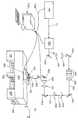
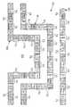
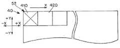
도1a는 본 발명에 따른 얇은 금속층의 측방향 응고(LS: lateral solidification) 가공을 수행하는 장치의 예시 실시예의 개략도이다.1A is a schematic diagram of an exemplary embodiment of an apparatus for performing lateral solidification (LS) processing of a thin metal layer in accordance with the present invention.
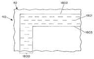
도1b는 확산 장벽층을 갖는 기판 상에 배치된 얇은 금속층을 갖는 제1 예시 샘플의 부분 단면도이다.FIG. 1B is a partial cross-sectional view of a first exemplary sample having a thin metal layer disposed on a substrate having a diffusion barrier layer.
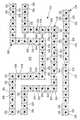
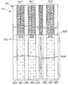
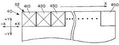
도2a 내지 도2i는 본 발명의 방법의 제1 예시 실시예에 따른 LS 가공의 상이한 단계에서 조사 빔 펄스 강도 패턴과 비교적 협소한 금속층 스트립의 결정립 구조를 도시하고 있다.2A-I show the grain structure of a metal layer strip relatively narrow with the irradiation beam pulse intensity pattern at different stages of LS processing according to the first exemplary embodiment of the method of the present invention.
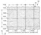
도3a 내지 도3e는 본 발명의 방법의 제2 예시 실시예에 따른 LS 가공의 상이한 단계에서 조사 빔 펄스 강도 패턴과 비교적 협소한 금속층 스트립의 결정립 구조를 도시하고 있다.3A-3E illustrate the grain structure of a metal layer strip relatively narrow with the irradiation beam pulse intensity pattern at different stages of LS processing in accordance with a second exemplary embodiment of the method of the present invention.
도4a는 확산 장벽층을 갖는 기판의 홈에 배치된 얇은 금속층을 갖는 제2 예시 샘플의 단면도이다.4A is a cross-sectional view of a second exemplary sample having a thin metal layer disposed in a groove of a substrate having a diffusion barrier layer.
도4b는 도4a의 제2 예시 샘플의 평면도이다.4B is a top view of the second example sample of FIG. 4A.
도4c는 도4a의 제2 예시 샘플의 등각도(isometric view)이다.FIG. 4C is an isometric view of the second example sample of FIG. 4A.
도5는 도1a의 장치에 의해 수행될 수도 있는 본 발명의 방법에 따라 적어도 부분적인 컴퓨터 제어 하에서의 예시적인 LS 가공을 나타내는 흐름도이다.FIG. 5 is a flow diagram illustrating exemplary LS processing under at least partial computer control in accordance with the method of the present invention that may be performed by the apparatus of FIG. 1A.
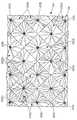
도6a 내지 도6f는 조사 빔 펄스의 강도 패턴이 비교적 작은 도트형 섀도우 영역의 배열을 갖는 본 발명의 방법의 제3 예시 실시예에 따른 LS 가공의 상이한 단계에서 조사 빔 펄스 강도 패턴과 금속층의 일부의 결정립 구조를 도시하고 있다.6A-6F illustrate a portion of the irradiation beam pulse intensity pattern and the metal layer at different stages of LS processing in accordance with a third exemplary embodiment of the method of the present invention having an arrangement of dot shadow areas where the intensity pattern of the irradiation beam pulses is relatively small. The grain structure of is shown.
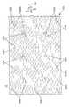
도7a 내지 도7h는 조사 빔 펄스의 강도 패턴이 서로에 대해 엇갈려 있는 규칙적으로 이격되는 반복형 셰브런 형태의 빔릿을 갖는 본 발명의 방법의 제4 예시 실시예에 따른 LS 가공의 상이한 단계에서 조사 빔 펄스 강도 패턴과 금속층의 일부의 결정립 구조를 도시하고 있다.7A-7H show the irradiation beams at different stages of LS processing according to a fourth exemplary embodiment of the method of the present invention with regularly spaced repeating chevron shaped beamlets in which the intensity patterns of the irradiation beam pulses are staggered with respect to each other. The pulse intensity pattern and the grain structure of a part of the metal layer are shown.
도8a 내지 도8d는 조사 빔 펄스의 강도 패턴이 규칙적으로 이격되고 비교적 협소한 선형의 스트라이프형 섀도우 영역과, 섀도우 영역들의 각각의 인접한 영역들 사이에서 인접하여 위치된 상태의 규칙적으로 이격되고 비교적 넓은 선형의 스 트라이프형 빔릿을 갖는 본 발명의 방법의 제5 예시 실시예에 따른 LS 가공의 다양한 단계에서 조사 빔 펄스 강도 패턴과 금속층의 일부의 결정립 구조를 도시하고 있다.8A to 8D show regularly spaced and relatively wide, with the intensity pattern of the irradiation beam pulses being regularly spaced and relatively narrow, with a linear striped shadow area and located adjacent between each adjacent areas of the shadow areas. The irradiation beam pulse intensity pattern and the grain structure of a portion of the metal layer are shown at various stages of LS processing in accordance with a fifth exemplary embodiment of the method of the present invention having a linear stripe beamlet.
도9a 내지 도9b는 조사 빔 펄스의 강도 패턴의 섀도우 영역 및 빔릿이 각각의 인접한 맞닿음 입계들 사이에서 연장되는 대각선으로 배향된 결정립을 얻도록 X 및 Y방향에 대해 대각선으로 배향되는 본 발명의 방법의 제5 예시 실시예의 변형예를 사용하여 얻어진 조사 빔 펄스 강도 패턴과 금속층 결정립 구조를 도시하고 있다.9A-9B illustrate the shadow regions of the intensity pattern of the irradiation beam pulses and the beamlets diagonally oriented with respect to the X and Y directions to obtain diagonally oriented grains extending between each adjacent abutment grain boundaries. The irradiation beam pulse intensity pattern and the metal layer grain structure obtained using the modification of the fifth exemplary embodiment of the method are shown.
도10a 내지 도10e는 제5 예시 실시예의 확장예인 본 발명의 방법의 제6 예시 실시예에 따른 LS 가공의 다양한 단계에서 조사 빔 펄스 강도 패턴과 금속층의 일부의 결정립 구조를 도시하고 있다.10A to 10E show the irradiation beam pulse intensity pattern and the grain structure of a part of the metal layer at various stages of LS processing according to the sixth exemplary embodiment of the method of the present invention, which is an extension of the fifth exemplary embodiment.
도11a 내지 도11d는 조사 빔 펄스의 강도 패턴이 규칙적인 간격으로 금속층 스트립에 중첩하는 복수개의 비교적 협소한 선형의 스트라이프형 섀도우 영역과, 이 섀도우 영역에 의해 중첩되지 않는 금속층 스트립의 모든 영역에 중첩하는 빔릿을 갖는 본 발명의 방법의 제7 예시 실시예에 따른 LS 가공의 다양한 단계에서 조사 빔 펄스 강도 패턴과 금속층 스트립의 결정립 구조를 도시하고 있다.11A-11D show a plurality of relatively narrow linear striped shadow areas in which the intensity pattern of the irradiation beam pulses overlaps the metal layer strips at regular intervals, and overlaps all areas of the metal layer strips not overlapped by the shadow areas. The irradiation beam pulse intensity pattern and the grain structure of the metal layer strip are shown at various stages of LS processing according to the seventh exemplary embodiment of the method of the present invention having a beamlet.
도12a 내지 도12d는 펄스형 조사 빔의 강도 패턴이 규칙적으로 이격되고 비교적 협소한 선형의 스트라이프형 섀도우 영역과, 각각의 인접한 섀도우 영역들 사이에서 인접하여 위치된 상태의 규칙적으로 이격되고 비교적 넓은 선형의 스트라이프형 빔릿을 갖고 금속층 스트립의 각각의 구역은 섀도우 영역 및 빔릿에 대해 대 각선으로 배향되는 본 발명의 방법의 제8 예시 실시예에 따른 LS 가공의 다양한 단계에서 조사 빔 펄스 강도 패턴과 직각 절곡부(bend)를 갖는 금속층 스트립의 결정립 구조를 도시하고 있다.12A-12D show a regularly spaced and relatively wide linear, with the intensity pattern of the pulsed irradiation beam being regularly spaced and relatively narrow linear striped shadow areas and located adjacent between each adjacent shadow areas. Each region of the strip of metal layer with a stripe beamlet of s is bent at right angles to the irradiation beam pulse intensity pattern at various stages of LS processing according to the eighth exemplary embodiment of the method of the present invention with the shadow areas and the diagonals oriented with respect to the beamlets. The grain structure of a metal layer strip having a bend is shown.
도13a 내지 도13c는 본 발명의 방법의 제9 예시 실시예에 따른 입계의 각각의 위치에서 금속층 스트립에 대해 큰 각도로 입계에 의해 분리되는 단일 결정립 영역을 갖는 금속층 스트립 형성의 상이한 단계를 도시하고 있다.13A-13C illustrate the different steps of forming a metal layer strip having single grain regions separated by grain boundaries at a large angle relative to the metal layer strip at each position of the grain boundary according to the ninth exemplary embodiment of the method of the present invention. have.
도14는 설명의 간략화를 위해 고정된 펄스형 조사 빔의 위치 및 조사 경로가 병진 이동 샘플의 기준 프레임에 도시되어 있는 본 발명의 방법의 제10 예시 실시예에 따른 연속 LS 가공을 수행한 금속층을 도시하고 있다.14 shows a metal layer subjected to continuous LS processing in accordance with a tenth exemplary embodiment of the method of the present invention in which the position and irradiation path of a fixed pulsed irradiation beam are shown in a reference frame of a translationally moving sample for simplicity of explanation. It is shown.
도15a 내지 도15g는 본 발명의 방법의 제10 예시 실시예에 따른 LS 가공의 상이한 단계에서 예시적인 조사 빔 펄스 강도 패턴과 도14에 도시된 금속층의 열의 일부의 결정립 구조를 도시하고 있다.15A-15G illustrate an exemplary irradiation beam pulse intensity pattern and a grain structure of a portion of the rows of metal layers shown in FIG. 14 at different stages of LS processing in accordance with a tenth exemplary embodiment of the method of the present invention.
도16a 내지 도16g는 가공을 위해 금속층을 구역들로 세분하여 구역마다 본 발명에 따른 금속층의 LS 가공을 수행하는 것을 도시하는 개략도이다.16A-16G are schematic diagrams illustrating subdividing the metal layer into zones for processing to perform LS processing of the metal layer according to the invention per zone.
상세한 설명details
도1a를 참조하면, 본 발명에 의한 얇은 금속층의 측방향 응고 가공(LS 가공)을 수행하기 위한 장치의 전형적인 실시예가 도시된다. 이러한 전형적인 장치는 람다 피직 모델(Lambda Physik model) LPX-315I XeCl 펄스형 엑시머 레이저(110)와, 마이크로라스 2판 가변 감쇠기(130; MicroLas two-plate variable attenuator) 와, 빔 조향 미러(140, 143, 147, 160, 162)와, 빔 신장 및 시준 렌즈(141, 142)와, 마이크로라스 빔 호모제나이저(144; MicroLas beam homogenizer)와, 콘덴서 렌즈(145)와, 시야 렌즈(148; field lens)와, (도시되지 않은) 병진 이동 스테이지(translating stage)에 장착될 수도 있는 투영 마스크(150; projection mask)와, 4배 내지 6배 대안 렌즈(161; eyepiece)와, 빈센트 어소시에이츠 유니블리쯔 모델 D122 조절형 셔터(152; Vincent Associates UniBlitz Model D122 controllable shutter)와, 샘플 병진 이동 스테이지(180) 상에 장착된 LS 가공될 얇은 금속층(52)을 갖는 샘플(40) 상으로 입사 조사 빔 펄스(164)를 집속하기 위한 다중 요소 대물 렌즈(163)와, 진동 절연 및 자동 수평 조절 시스템(191, 192, 193, 194) 상에서 지지되는 그래나이트 블록 광학대(190)와, 펄스형 엑시머 레이저(110), 빔 에너지 밀도 변조기(120), 가변 감쇠기(130), 셔터(152) 및 샘플 병진 이동 스테이지(180)를 제어하도록 결합된 사이버리서치 인크(CyberResearch Inc.)의 (펜티엄 프로세서 Ⅲ가 윈도우즈 ME를 작동시키는) 인더스트리얼 컴퓨터 시스템 컴퓨터(106)를 포함한다. 샘플 병진 이동 스테이지(180)는 X, Y 및 Z 방향으로 샘플(400의 병진 이동 및 미세 병진 이동을 수행하도록 컴퓨터(106)에 의해 제어된다. 펄스형 엑시머 레이저 대신에 펄스형 조사 빔 소스(110; beam source)가 펄스형 고체 레이저, 쵸핑된 연속파 레이저, 펄스형 전자 빔 또는 펄스형 이온빔과 같이 소스(110)로부터 샘플(40)로의 조사 빔 경로를 적절히 변경함으로써 후술하는 방법으로 얇은 금속층을 용융하기에 적합한 짧은 에너지 펄스를 갖는 다른 공지된 소스일 수도 있다는 것을 당업자는 알 수 있다. 도1a의 전형적인 장치 실 시예의 컴퓨터(106)는 금속층(52)의 LS 처리를 수행하기 위해 샘플(40)의 미세 병진 이동을 제어하면서, 금속층(52)에 대해 조사 빔 펄스의 강도 패턴을 이동시키기 위해 (도시되지 않은) 적절한 마스크 병진 이동 스테이지 내에 장착된 마스크(150)의 미세 병진 이동을 제어하도록 구성될 수도 있다. 도1a의 전형적인 장치는 이하 설명될 방법으로 샘플(40) 상의 금속층(52)의 LS 가공을 수행하는 데에 사용될 수도 있다.Referring to Fig. 1A, a typical embodiment of an apparatus for performing lateral solidification (LS machining) of a thin metal layer according to the present invention is shown. Such a typical device is a Lambda Physik model LPX-315I XeCl pulsed
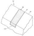
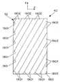
도1b에 의하면, 전형적인 샘플(40)의 단면도가 도시되어 있다. 샘플(40)은 확산 장벽층(51)을 갖는 기판(51)과, 이 확산 장벽층의 위에 위치하는 금속층(52)을 포함한다. 기판(51)은 그 내부에 부분적으로 또는 완전히 제작된 집적 회로 장치를 갖는 반도체 기판일 수도 있다. 금속층(52)은 하나 이상의 집적 회로 장치의 복수의 금속 상호 연결 라인이거나, 또는 이러한 상호 연결 라인으로 패터닝되기 전의 또는 다른 적용예에 사용되기 위한 연속형 금속층일 수도 있다. 확산 장벽층(51)은 산화규소(SiO2) 층, 탄탈룸(Ta) 층, 탄탈룸을 함유하는 조성으로 이루어진 층, 또는 금속층(52)의 재료의 하부 기판(50)으로의 확산을 방지하고 그 상에서 금속 결정립의 측방향 성장을 허용하는 다른 임의의 적절한 재료로 이루어진 층일 수도 있다. 금속층(52)이 배치되는 확산 장벽 또는 임의의 기판 표면이 금속층(52) 내의 결정립 성장을 유도(seed)해서는 안된다는 것을 알 수 있다.1B, a cross-sectional view of a
금속층(52)은 종래의 기술, 예컨대 당업자에게 널리 알려진 화학 기상 증착(CVD) 공정, 물리 기상 증착(PVD) 공정 또는 전기화학 증착 공정을 이용하여 기판(50)의 확산 장벽층(51) 상에 증착된다. 금속층(52)은 집적 회로 장치 내의 상호 연결 라인을 형성하는 데에 적합하거나 또는 다른 적용예에 이용하기에 적합한 알루미늄, 구리, 텅스텐, 티타늄, 백금 또는 금과 같은 임의의 단원소 금속, 합성 금속 또는 합금으로 이루어질 수도 있다. 또한, 확산 장벽층(51)의 재료는 금속층(52)이 용융될 때 용융된 금속이 확산 장벽층(51)의 표면을 적절히 "적시도록"(wet) 선택되는 것이 효과적이다. 이러한 "적심" 현상은 용융될 때의 금속층(52)이 확산 장벽층(51) 상에 균일하게 배치될 수 있게 하여, 용융된 금속층(52)의 응집을 방지한다. 그러나, 용융될 때의 금속층(52)에 의한 확산 장벽층(51)의 "적심" 현상은 금속층(52)을 용융시키기 위해 보다 짧은 (예컨대, 30 나노초 이하의 펄스 지속 시간을 갖는) 조사 빔 펄스를 이용함으로써 이러한 응집이 회피될 수도 있기 때문에 반드시 필요한 것은 아니다.The
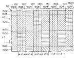
본 발명의 제1 실시예에 의한 방법을 도2a 내지 도2i를 참조하여 설명한다. 도2a에 도시된 바와 같이, 부분 제작된 집적 회로 장치와 같은 샘플(40)의 전형적인 영역은 함께 금속층(52)을 구성하는 3개의 얇은 금속층 스트립(80, 81, 82)을 갖는다. 예컨대 종래의 금속 증착 및 포토리소그래피 및 에칭에 의한 종래의 패터닝에 의해 구리로 형성된 이들 금속층 스트립(80, 81, 82)은 작은 결정립과 그 내부에서 다양한 방향으로 랜덤하게 배향된 입계를 갖는다. 금속층 스트립(80, 81, 82)의 폭은 통상 0.1㎛ 내지 10㎛의 범위이고, 용융된 금속층 스트립의 두께는 통상 0.1㎛ 이하에서 10㎛의 범위이다. 처리되는 금속층(52)이 부분 제작된 전체 집적 회로 장치 또는 다중의 부분 제작된 집적 회로의 금속 상호 연결 라인을 샘플(40)로서의 반도체 웨이퍼 상에 구비할 수도 있다는 것을 명심해야 한다. 실질적으로, 전체적인 현대적 VLSI 집적 회로 장치의 소정의 금속 수준 내에 있는 금속 상호 연결 라인의 개수는 만 이상의 정도일 수 있다. 또한, 이러한 상호 연결 라인은 도2a 내지 도2i에 도시된 전형적인 금속층 스트립의 길이보다 훨씬 긴 길이만큼 연장할 수 있다.The method according to the first embodiment of the present invention will be described with reference to Figs. 2A to 2I. As shown in FIG. 2A, a typical region of a
전술한 바와 같이, 작은 결정립과 랜덤하게 배향된 입계를 갖는다는 것은 전자 이동 측면에서 바람지하지 못하고, 높은 전류 밀도를 전송하기 위한 상호 연결 라인으로 사용될 때 이들 금속층 스트립(80, 81, 82) 중의 하나 이상에 바람직하지 않게 높은 불량률을 초래할 수도 있다. 집적 회로 장치의 상호 연결 라인은 "맨해튼 형상"(Manhattan geometry)을 가지며, 즉 각각의 상호 연결 라인은 직선이거나 이들 상호 연결 라인의 인접 세그먼트에 대해 단지 90°의 각도로 방향을 바꾼다. 본 발명의 LS 공정은 금속층 스트립의 인접 세그먼트에 대해 90°이외의 각도로 방향을 바꾸거나 금속층 스트립이 곡면 형상을 갖는 경우에 금속층 스트립을 가공하는 데에 동일하게 적용될 수 있다는 것을 알 수 있다.As mentioned above, having small grains and randomly oriented grain boundaries do not wind in terms of electron transfer, and when used as interconnect lines for transmitting high current densities, these metal layer strips (80, 81, 82) At least one may result in an undesirably high failure rate. The interconnect lines of the integrated circuit device have a "Manhattan geometry", ie each interconnect line is straight or redirects at an angle of only 90 ° with respect to adjacent segments of these interconnect lines. It can be seen that the LS process of the present invention can be equally applied to machining metal layer strips in a direction other than 90 ° relative to adjacent segments of the metal layer strips or when the metal layer strip has a curved shape.
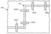
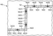
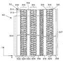
도2b에 의하면, 소정의 강도 패턴을 갖는 제1 조사 빔 펄스로써 조사된 후의 금속층 스트립(80, 81, 82)이 도시되어 있다. 본 실시예에서, 조사 빔 펄스는 308㎚의 파장을 갖는 XeCl 엑시머 레이저 빔 펄스이다. 도1a에 의하면, 조사 빔 펄스는 엑시머 레이저(100)에 의해 발생되고, 마스크(150)는 조사 빔 펄스의 소정의 강도 패턴을 형성하는 데에 사용된다. 도2b에 도시된 바와 같이, 제1 조사 빔 펄스의 강도 패턴은 마스크(150)에 의해 형성되는 바와 같이 복수의 균등 이격된 도트 형 "섀도우 영역"(61)의 각 시리즈를 포함하며, 여기서 각 금속층 스트립(80, 81, 82) 내의 각각의 섀도우 영역(61)에 의해 중첩된 영역들로의 조사를 방지하기 위해 빔 강도는 마스크(150)에 의해 전적으로 차단된다. 제1 조사 빔 펄스의 경우, 각각의 도트형 섀도우 영역(61)은 중심선을 따라 일정한 간격으로 금속층 스트립(80, 81, 82) 중의 각각의 하나와 중첩된다. 제1 조사 빔 펄스의 강도 패턴은 각각의 섀도우 영역(61)에 의해 중첩되지 않는 금속층 스트립(80, 81, 82)의 모든 영역들과 중첩하고 최대 조사 빔 강도를 갖는 "빔릿"을 또한 구비한다.2B, metal layer strips 80, 81, 82 are shown after being irradiated with a first irradiation beam pulse having a predetermined intensity pattern. In this embodiment, the irradiation beam pulse is an XeCl excimer laser beam pulse having a wavelength of 308 nm. 1A, the irradiation beam pulses are generated by the
금속층 스트립(80, 81, 82)이 마스크(150)에 의해 형성된 강도 패턴을 갖는 제1 조사 빔 펄스에 의해 조사될 때, 빔릿에 의해 중첩되는 각각의 금속층 스트립(80, 81, 82)은 전체 두께에 걸쳐 용융되는 반면에, 각각의 섀도우 영역(61)에 의해 중첩되는 금속층 스트립(80, 81, 82)의 각각은 적어도 부분적으로 미용융 상태로 유지되어 이들이 형성될 때 금속층 스트립(80, 81, 82)의 원래의 결정립 구조를 갖는다. 원 또는 정사각형 등의 임의의 형상을 가질 수도 있는 섀도우 영역(61)은 작은 면적을 갖지만, 주변의 용융된 금속층으로부터의 열 확산이 각각의 섀도우 영역(61)에 의해 중첩된 완전 용융 영역을 초래하지 않는 정도로 충분히 크다. 본 발명에 의하면, 각각의 섀도우 영역에 의해 중첩된 영역들은 적어도 부분적으로는 미용융 상태로 유지되어야 한다. 통상, 엑시머 레이저(110)로부터의 조사 빔 펄스는 10 내지 104mJ/㎠ 범위의 빔릿 강도와 10 내지 103 ㎱ 범위의 펄스 지속시간과, 10㎐ 내지 104㎐ 범위의 펄스 반복율을 제공한다. 도1a의 장치 내의 펄스형 엑시머 레이저(110)에 의해 제공되는 조사 빔 펄스의 에너지 제한을 받기 때문에, 마스크(150)에 의해 형성되는 조사 빔 펄스의 강도 패턴은 전체 웨이퍼 상의 부분 제작된 전체 집적 회로 장치의 모든 금속 상호 연결 라인, 복수의 부분 제작된 집적 회로 장치의 모든 금속 상호 연결 라인 또는 부분 제작된 모든 집적 회로 장치의 모든 금속 상호 연결 라인을 조사할 수도 있다.When the metal layer strips 80, 81, 82 are irradiated by a first irradiation beam pulse having an intensity pattern formed by the
도2c로 돌아가면, 금속층 스트립(80, 81, 82)이 제1 조사 빔 펄스에 의해 조사된 후 금속층 스트립(80, 81, 82)의 용융 영역은 냉각되어 재응고될 수 있다. 적어도 부분적인 미용융 영역(63)이 금속층 스트립(80, 81, 82)의 원래의 결정립 구조를 가지므로, 각각의 적어도 부분적인 미용융 영역(63) 내의 이러한 결정립 구조는 금속층 스트립(80, 81, 82)의 재응고되어 용융된 인접 영역으로 결정립의 측방향 성장을 유도한다. 각 용융 영역의 이러한 재응고 중에, 각각의 금속층 스트립(80, 81, 82) 내의 적어도 부분적인 미용융 영역(63)을 막 둘러싼 각각의 재응고 영역(55) 내의 각각의 적어도 부분적인 미용융 영역(63)으로부터 외향으로 성장한다. 각각의 재응고 영역(55)은 각각의 금속층 스트립(80, 81, 82)의 모서리에 의해 그리고 인접한 적어도 부분적인 미용융 영역(63)으로부터 성장하는 결정립을 갖는 재응고 영역(55) 내에서 적어도 부분적인 미용융 영역(63)으로부터 성장하는 결정립의 인접 부분에 의해 경계가 정해진다. 인접한 적어도 부분적인 미용융 영역(63)으로부터 성장하는 결정립이 인접하기 전에 각각의 적어도 부분적인 미용융 영역으로부터 성장하는 결정립들의 맞닿음 결정립 성장 거리는 빔릿의 폭에 의해 한정되는 바와 같이 용융 영역의 폭의 절반이 된다. 이러한 방법으로, 금속층 스트립(80, 81, 82)의 용융 영역의 재응고가 종료된 후, 큰 결정립(62)이 각각의 재응고 영역(55) 내에 형성된다. 인접 섀도우 영역(61) 사이의 간격은, 금속층 스트립(80, 81, 82)의 용융 영역의 재응고가 종료되기 전에 (즉, 새로운 결정립의 핵 형성이 개재 공간에서 발생하기 전에) 각각의 섀도우 영역(61)에 의해 중첩되는 각각의 적어도 부분적인 미용융 영역(63)으로부터 성장하는 결정립들이 적어도 2개의 적어도 부분적인 미용융 영역(63)으로부터 성장하는 결정립과 인접하도록 설정되어야 한다. 결정립들의 특성 성장 거리는 새로운 결정립의 핵 형성이 발생하기 전에 이 결정립들이 성장하는 거리이다.Returning to FIG. 2C, the molten region of the metal layer strips 80, 81, 82 can be cooled and resolidified after the metal layer strips 80, 81, 82 are irradiated by the first irradiation beam pulse. Since the at least partial
적어도 부분적인 미용융 영역(63)으로부터의 결정립의 성장이 금속층 스트립의 모서리에 도달하지 않고/않거나 용융 영역이 완전히 재응고하기 전에 인접한 적어도 부분적인 미용융 영역으로부터 성장하는 결정립과 인접하지 않게 될 만큼 상호 연결 라인 세그먼트(80, 81, 82)의 폭이 큰 경우에, 각각의 섀도우 영역에 의해 중첩되는 각각의 적어도 부분적인 미용융 영역으로부터 성장하는 결정립들이 각각의 금속층 스트립(80, 81, 82)의 모서리에 도달하거나 또는 용융 영역의 재응고가 종료되기 전에 인접한 적어도 부분적인 미용융 영역으로부터 성장하는 결정립들과 인접하도록 마스크(150)는 금속층 스트립(80, 81, 82)의 각각의 모서리에 그리고 상호간에 충분히 근접하게 이격된 섀도우 영역의 적절한 배열을 갖는 강도 패턴을 형성해야 한다.The growth of the grains from the at least partially
도2d로 돌아가면, 펄스형 조사 빔(164)의 금속층 스트립(80, 81, 82) 상으로 충돌 위치가 바람직하게는 고정되므로, 샘플(40)은 제2 조사 빔 펄스의 강도 패턴 의 섀도우 영역(64)의 각각이 제1 조사 빔 펄스의 강도 패턴의 섀도우 영역(61)의 금속층 스트립 상의 위치에 대해 제1 조사 빔 펄스에 이어 최대 맞닿음 결정립 성장 거리보다 작은 거리만큼 다소 이동하도록 컴퓨터(106)의 제어 하에 샘플 병진 이동 스테이지(180)에 의해 다시 위치 설정된다. 맞닿음 결정립 성장 거리는 하나의 결정립이 동일한 용융 영역 내에서 성장하는 다른 결정립과 인접하기 전에 그리고 용융된 층의 모서리와 인접하기 전에 인접 용융 영역 내의 적어도 부분적인 미용융 영역으로부터 성장하는 거리이다. 이러한 방법으로, 각각의 섀도우 영역(64)은 제1 조사 빔 펄스에 의한 조사 후에 형성된 동일한 재응고 영역(55) 내의 다른 영역과 중첩한다. 예컨대, 새로운 섀도우 영역(64)의 위치는 섀도우 영역(61)의 이전 위치로부터 0.01 내지 10㎛ 범위의 거리만큼 이동된다. 이러한 미세한 재위치 설정은 이하에서 "미세 병진 이동"이라 한다. 선택적으로, 제2 조사 빔 펄스의 강도 패턴의 섀도우 영역(64)의 소정의 이동을 얻기 위해 샘플(40) 대신에 마스크(150)가 병진 이동될 수도 있다. 제2 조사 빔 펄스의 강도 패턴의 빔릿이 제1 조사 빔 펄스의 강도 패턴의 빔릿에 대해 이동하더라도, 이동된 빔릿은 각각의 이동된 섀도우 영역(64)에 의해 중첩되지 않은 금속층 스트립(80, 81, 82)의 모든 영역과 여전히 중첩하고 있다.Returning to FIG. 2D, since the impact location is preferably fixed onto the metal layer strips 80, 81, 82 of the
도2d에 도시된 바와 같이, 샘플(40)의 상기 미세 병진 이동 후에, 도1a의 장치는 제2 조사 빔 펄스로써 금속층 스트립(80, 81, 82)을 조사하며 그 결과 이동된 빔릿에 의해 중첩되는 금속층 스트립(80, 81, 82)의 각각의 영역이 그 전체 두께에 걸쳐 용융되며, 각각의 이동된 섀도우 영역(64)에 의해 중첩되는 금속층 스트립의 각각의 영역은 적어도 부분적인 미용융 상태로 유지된다. 적어도 부분적인 미용융 영역의 각각은 각각의 인접 용융 영역과 인접한다. 각각의 이동된 섀도우 영역(64)이 제1 조사 빔 펄스의 강도 패턴의 대응 섀도우 영역(61)의 각각에 의해 중첩되는 영역과 동일한 재응고 영역(55) 내의 영역과 중첩한다. 예를 들면, 샘플(40)은 반시계 방향으로의 회전 각도를 양(positive)으로 볼 때 X축에 대해 -135도인 -A 방향으로 미세 병진 이동하거나, X축에 대해 45도의 각도인 +A 방향으로 미세 병진 이동할 수 있다.As shown in FIG. 2D, after the micro-translational movement of the
도2e에 의하면, 제2 조사 빔 펄스에 의한 조사에 이어지는 용융 영역의 재응고 후의 금속층 스트립(80, 81, 82)이 도시된다. 샘플(40)의 미세 병진 이동 및 제2 조사 빔 펄스에 의한 조사 후의 적어도 부분적인 미용융 영역(65)의 각각이 제1 조사 빔 펄스에 의한 조사 후의 적어도 부분적인 미용융 영역(63)의 각각에 함유된 것보다 작은 개수의 결정립을 함유하고 있으므로, 제2 조사 빔 펄스에 의한 조사 후의 금속층 스트립(80, 81, 82)의 각각의 용융 영역의 재응고시 새로운 재응고 영역(55')들 중의 대응되는 한 영역 내에서 성장할 결정립이 동일하거나 더 많게 될 것이다. 도2e에 도시된 바와 같이, 결정립의 성장은 각각의 금속층 스트립(80, 81, 82)의 모서리에 도달하거나 또는 새로운 재응고 영역(55')을 형성하기 위해 인접한 이동된 적어도 부분적인 미용융 영역(65)으로부터 성장하는 결정립들과 인접하도록 각각의 이동된 적어도 부분적인 미용융 영역(65)으로부터 측방향으로 발생하며, 이 경우 맞닿은 결정립은 각각의 맞닿음 결정립 성장 거리만큼 성장한다. 도2e에 의하면, 각각의 새로운 재응고 영역(55')은 도2c에 도시된 이전 의 재응고 영역(55)보다 개수가 더 적고 크기가 더 큰 결정립(66)을 갖는다.According to FIG. 2E, the metal layer strips 80, 81, 82 after resolidification of the molten region following the irradiation with the second radiation beam pulse are shown. Each of the at least partial
도2f에 의하면, 제2 조사 빔 펄스에 의한 조사에 이은 용융 영역의 재응고가 종료된 후, 샘플(40)은 제3 조사 빔 펄스의 강도 패턴의 2회 이동된 섀도우 영역(67)이 각각의 재응고 영역(55) 내의 다른 영역과 각각 중첩하도록 제2 조사 빔 펄스 이후에 최대 맞닿음 결정립 성장 거리보다 작은 거리만큼 임의의 방향으로 펄스형 조사 빔(164)에 대해 미세 병진 이동한다. 도2f에 도시된 실시예에서, 추가 미세 병진 이동의 방향(B)은 X축에 대해 45도의 각도이다. 샘플(40)이 상기 방향으로 미세 병진 이동한 후, 금속층 스트립(80, 81, 82)은 마스크(150)에 의해 형성된 동일한 강도 패턴을 갖는 제3 조사 빔 펄스에 의해 조사되나, 이 경우 섀도우 영역(67)은 각각 2회 이동되었다. 2회 이동된 섀도우 영역(67)은 각각의 이전 섀도우 영역(64)으로부터 제2 조사 빔 펄스 후의 최대 맞닿음 결정립 성장 거리보다 작은 거리만큼, 예컨대 0.01 내지 10㎛ 범위의 거리만큼 이동된다. 비록 제3 조사 빔 펄스의 강도 패턴의 빔릿이 제2 조사 빔 펄스의 강도 패턴의 빔릿에 대해 또한 이동하더라도, 2회 이동된 빔릿은 2회 이동된 섀도우 영역(67)의 각각에 의해 중첩되지 않는 금속층 스트립(80, 81, 82)의 모든 영역과 여전히 중첩된다.According to FIG. 2F, after the resolidification of the melting region following the irradiation by the second irradiation beam pulse is finished, the
도2g에 의하면, 제3 조사 빔 펄스의 조사 및 용융 영역의 재응고 종료 후의 재응고된 금속층 스트립(80, 81, 82)이 도시된다. 2회 이동된 적어도 부분적인 미용융 영역(71)이 각각 1회 이동된 적어도 부분적인 미용융 영역(65)에 함유된 것보다 작은 개수의 결정립을 함유하고 있기 때문에, 제3 조사 빔 펄스에 의한 조사 후의 금속층 스트립(80, 81, 82)의 각각의 용융 영역의 재응고의 종료시 새로운 재응 고 영역(69)들 중의 대응되는 하나의 영역 내에서 성장할 결정립이 동일하거나 더 적게 될 것이다. 도2g에 도시된 바와 같이, 결정립의 성장은 각각의 금속층 스트립(80, 81, 82)의 모서리에 도달하거나 또는 새로운 재응고 영역(69)을 형성하기 위해 인접한 2회 이동된 적어도 부분적인 미용융 영역(71)으로부터 성장하는 결정립들과 인접하도록 각각의 2회 이동된 적어도 부분적인 미용융 영역(71)으로부터 측방향으로 발생하며, 이 경우 맞닿은 결정립은 각각의 맞닿음 결정립 성장 거리만큼 성장한다. 도2g에 의하면, 각각의 새로운 재응고 영역(69)은 도2e에 도시된 이전의 재응고 영역(55')보다 개수가 더 적고 크기가 더 큰 결정립(66)을 갖는다.2G shows the resolidified metal layer strips 80, 81, 82 after the irradiation of the third irradiation beam pulse and the end of resolidification of the molten region. Since the at least partial
도2h에 의하면, 제3 조사 빔 펄스의 조사에 이은 각각의 용융 영역의 재응고가 종료된 후, 샘플(40)은 제4 조사 빔 펄스의 강도 패턴의 3회 이동된 섀도우 영역(63)이 각각의 재응고 영역(69) 내의 다른 영역과 각각 중첩하도록 제3 조사 빔 펄스 이후의 최대 맞닿음 결정립 성장 거리보다 작은 거리만큼 임의의 방향으로 펄스형 조사 빔(164)에 대해 미세 병진 이동한다. 도6h에 도시된 실시예에서, 추가 미세 병진 이동의 방향(C)은 X축에 대해 -135도의 각도이고, 이 추가 미세 병진 이동의 거리는 0.01 내지 10㎛ 범위이다. 샘플(40)이 상기 방향으로 상기 거리만큼 미세 병진 이동한 후, 금속층 스트립(80, 81, 82)은 도2f에 도시된 제3 조사 빔 펄스와 동일한 강도 패턴을 갖는 제4 조사 빔 펄스에 의해 조사되나, 이 경우 섀도우 영역(72)과 빔릿은 금속층 스트립(80, 81, 82)에 대해 각각 3회 이동되었다.According to FIG. 2H, after resolidification of each melting region following irradiation of the third irradiation beam pulse is finished, the
도2i에 의하면, 제4 조사 빔 펄스의 조사 및 각각의 용융 영역의 재응고 종료 후의 재응고된 금속층 스트립(80, 81, 82)이 도시된다. 3회 이동된 적어도 부 분적인 미용융 영역(73)에 의해 중첩되는 적어도 부분적인 미용융 영역(73)(즉, 3회 이동된 적어도 부분적인 미용융 영역)이 단일 결정립을 각각 함유하고 있기 때문에, 금속층 스트립(80, 81, 82)의 용융 영역의 재응고 종료시 새로운 재응고 영역(70)들 중의 대응되는 하나의 영역 내에서 성장할 결정립이 동일하거나 더 많게 될 것이다. 도2i에 도시된 바와 같이, 결정립의 성장은 각각의 금속층 스트립(80, 81, 82)의 모서리에 도달하거나 또는 새로운 재응고 영역(70)을 형성하기 위해 인접한 3회 이동된 적어도 부분적인 미용융 영역(73)으로부터 성장하는 결정립들과 인접하도록 각각의 3회 이동된 적어도 부분적인 미용융 영역(73)으로부터 측방향으로 발생한다. 도2i에 도시된 바와 같이, 금속층 스트립(80, 81, 82)의 새로운 재응고 영역(70)의 각각은 단일 결정립이고, 각각의 입계는 이 입계 위치에서 각각의 금속층 스트립(80, 81, 82)에 대해 수직하다. 그러므로, 금속층 스트립(80, 81, 82)이 집적 회로 장치의 상호 연결 라인부이면, 이들 상호 연결 라인부 내에서의 전자 이동은 사실상 감소된다. 도2a 내지 도2i를 참조하여 설명한 바와 같이, 각각의 금속층 스트립 내에 도2i에 도시된 소정의 결정립 구조를 얻기 위해, 금속층 스트립(80, 81, 82)이 많거나 적은 미세 병진이동, 조사 및 재응고 단계를 받게 된다는 것을 알 수 있다.According to FIG. 2I, the resolidified metal layer strips 80, 81, 82 after the irradiation of the fourth irradiation beam pulse and the end of resolidification of each melting region are shown. Since the at least partial unmelted regions 73 (ie, at least partially unmelted regions shifted three times) each overlapped by the at least partially
각각의 금속층 스트립(80, 81, 82) 내에 소정의 결정립 구조를 얻기 위한 전술한 LS 가공의 종료 후, 샘플(40)은 LS 가공용 후속 구역(next section)으로 병진 이동할 수도 있다. (도1a에 도시된) 새로운 마스크(150)는 마스크(150)에 의해 형성되는 바와 같이 조사 빔 펄스의 강도 패턴의 일련의 섀도우 영역이 각각의 금속 층 스트립의 형상을 따라야 하기 때문에 후속 구역이 금속층 스트립과 다른 구성을 가진다면 LS 가공을 필요로 할 것이다.After completion of the aforementioned LS processing to obtain the desired grain structure in each
본 발명의 제2 실시예에 의한 방법을 도3a 내지 도3e를 참조하여 설명한다. 명확히 하기 위해, 도2a 내지 도2i에 도시된 바와 같이 제1 실시예를 설명하기 위해 사용된 금속층 스트립(80, 81, 82)의 동일 구성을 본 실시예를 설명하는 데에 사용한다. 제1 실시예에서와 같이, 도3a에 도시된 금속층 스트립(80, 81, 82)은 예컨대 구리로 형성되고, 초기에는 작은 결정립과 랜덤하게 배향되는 입계를 갖는다. 각각의 금속층 스트립은 통상 0.1㎛ 내지 10㎛ 범위의 폭과 통상 0.1㎛ 이하 내지 10㎛ 범위의 두께를 갖는다.The method according to the second embodiment of the present invention will be described with reference to Figs. 3A to 3E. For clarity, the same configuration of the metal layer strips 80, 81, 82 used to describe the first embodiment as shown in Figs. 2A to 2I is used to describe this embodiment. As in the first embodiment, the metal layer strips 80, 81, 82 shown in Fig. 3A are formed of copper, for example, and initially have small grains and randomly oriented grain boundaries. Each metal layer strip typically has a width in the range of 0.1 μm to 10 μm and a thickness typically in the range of 0.1 μm to 10 μm.
도3b에 의하면, 금속층 스트립(80, 81, 82)은 (도1a에 도시된) 마스크(150)에 의해 형성되는 바와 같이 각각의 금속층 스트립(80, 81, 82)의 동일한 소정의 형상을 각각 갖는 상대적으로 폭이 좁은 3개의 스트라이프형 섀도우 영역(83)을 구비한 강도 패턴을 갖는 제1 조사 빔 펄스에 의해 조사된다. 이 섀도우 영역(83) 외에, 마스크(150)에 의해 형성되는 바와 같이 제1 조사 빔 펄스의 강도 패턴은 섀도우 영역(72)에 의해 중첩되지 않는 금속층 스트립(80, 81, 82)의 모든 영역과 중첩하는 빔릿을 또한 구비한다. 효과적으로는, 섀도우 영역(83)의 폭은 0.01 내지 5㎛ 범위이다. 처음에, 이 샘플(40)은 제1 조사 빔 펄스의 강도 패턴의 섀도우 영역(72)은 각 금속층 스트립의 중심선을 따라 각 금속층 스트립(80, 81, 82)과 중첩된다. 제1 조사 빔 펄스에 의해 조사될 때, 빔릿에 의해 중첩되는 금속층 스트립(80, 81, 82)의 각 영역은 전체 두께에 걸쳐 용융되는 반면에 각각의 섀도우 영역(72)에 의해 중첩되는 금속층 스트립의 각 영역은 적어도 부분적인 미용융 상태로 유지된다. 조사 빔 펄스의 강도 패턴의 섀도우 영역(83)은 각 금속층 스트립(80, 81, 82) 내의 용융 영역(85, 86)으로부터의 열 확산이 각 섀도우 영역(83)에 의해 중첩되는 금속층 스트립(80, 81, 82)의 영역들을 현저히 용융시키지 않는다. 제1 조사 빔 펄스에 의한 조사 후에, 각 금속층 스트립(80, 81, 82) 내의 적어도 부분적으로 용융되지 않는 영역(84)은 LS 가공 전의 금속층 스트립의 원래의 결정립 구조를 가질 것이다.According to FIG. 3B, the metal layer strips 80, 81, 82 each have the same predetermined shape of each
도3c에 의하면, 제1 조사 빔 펄스에 의한 조사 후의 각 금속층 스트립(80, 81, 82) 내의 용융 영역(85, 86)의 냉각 및 재응고시, 결정립의 측방향 성장은 금속층 스트립(80, 81, 82) 내의 적어도 부분적인 미용융 영역(84)의 각각으로부터 각 금속층 스트립의 모서리를 향해 외향으로 발생한다. 이러한 방법으로, 재응고 영역(87, 88)은 금속층 스트립에 대해 보다 큰 각도로 배향된 입계를 갖는 보다 큰 금속 결정립의 각각의 행(73, 74; row)을 각각 구비하는 상태로 각각의 금속층 스트립(80, 81, 82) 내에 형성된다.According to FIG. 3C, upon cooling and resolidification of the
도3d에 의하면, 제1 조사 빔 펄스에 의한 조사에 이어 각각의 금속층 스트립(80, 81, 82) 내에서의 용융 영역(85, 86)의 재응고의 종료 후에, 샘플(40)이 X축에 대해 -135도의 각도로 -A 방향으로 미세 병진 이동하거나 또는 (도1a에 도시된) 마스크(150)가 각각의 금속층 스트립(80, 81, 82) 내의 각각의 상부 행의 결정립(73)과 중첩하도록 제2 조사 빔 펄스의 강도 패턴의 섀도우 영역(76)을 이동시키기 위해 X축에 대해 45도 각도의 A 방향으로 미세 병진 이동한다. 샘플(40) 이나 마스크(150) 중의 하나 또는 이들 모두는 제2 조사 빔 펄스의 섀도우 영역(76)이 각 금속층 스트립(80, 81, 82) 내의 하부 행의 각각의 결정립(74)과 중첩하도록 미세 병진 이동된다. 제2 조사 빔 펄스의 강도 패턴의 빔릿이 제1 조사 빔 펄스의 강도 패턴의 빔릿에 대해 이동하더라도, 이동된 빔릿은 각각의 이동된 섀도우 영역(76)에 의해 중첩되지 않는 금속층 스트립(80, 81, 82)의 모든 영역과 여전히 중첩하고 있다. 섀도우 영역(76) 및 빔릿의 이동을 제외하고는, 제2 조사 빔 펄스의 강도 패턴은 제1 조사 빔 펄스의 강도 패턴과 동일하다.According to FIG. 3D, after completion of resolidification of the
샘플(40) 또는 마스크(150)의 미세 병진 이동 후, 금속층 스트립(80, 81, 82)은 제2 조사 빔 펄스에 의해 조사되며, 그 결과 이동된 빔릿에 의해 중첩되지 않는 금속층 스트립(80, 81, 82)의 각각의 영역은 그 전체 두께에 걸쳐 용융되는 반면에, 각각의 이동된 섀도우 영역(76)에 의해 중첩되는 금속층 스트립의 각각의 영역은 적어도 부분적인 미용융 상태로 유지된다. 적어도 부분적인 미용융 영역의 각각은 인접 용융 영역과 인접한다. 적어도 부분적인 미용융 영역은 원래의 금속층 스트립(80, 81, 82)의 결정립 및 입계보다 더 크고 입계가 금속층 스트립에 대해 보다 큰 각도를 형성하는 결정립을 함유하기 때문에, 각 금속층 스트립(80, 81, 82) 내의 용융 영역(77, 78)의 재응고시 상기의 큰 결정립은 각각의 금속층 스트립이 도3e에 도식적으로 도시된 바와 같이 입계의 각 위치에서 금속층 스트립에 대해 보다 큰 각도(즉, 90°에 근접하는 각도)로 배향되는 입계를 갖는 보다 큰 결정립을 가지도록 적어도 부분적인 미용융 영역(85)으로부터 금속층 스트립(80, 81, 82)의 모서리를 향해 각각의 방향으로 측방향으로 결정립의 성장을 유도한다.After the micro-translational movement of the
제2 조사 빔 펄스에 의한 조사에 이어 용융 영역(77, 78)의 재응고 후, 적절한 방향으로 샘플(40) 또는 마스크(150)의 미세 병진 이동의 추가 반복과 추가 조사 빔 펄스와 금속층 스트립의 각각의 용융 영역의 재응고는 각각의 금속층 스트립(80, 81, 82) 내의 결정립의 수를 감소시키면서 입계를 상기 입계의 각각의 위치에서 금속층 스트립에 대해 보다 큰 각도로 보다 일관되게 배향시키도록 하기 위해서 수행될 수도 있다. 전술한 실시예에서, 각각의 조사 빔 펄스는 10 내지 104 mJ/㎠ 범위의 빔릿 강도와 10 내지 103 ㎱ 범위의 펄스 지속시간(FWHM)과 10 내지 104 ㎐ 범위의 펄스 반복율을 통상적으로 갖는다.After reconsolidation of the
도3a 내지 도3e를 참조하여 전술한 바와 같이, 금속층 스트립(80, 81, 82)의 LS 가공의 종료 후, 샘플(40)은 LS 가공을 위한 금속층 스트립의 후속 구역으로 병진 이동될 수도 있다. 이 후속 구역이 도3a 내지 도3e에 도시된 것과는 다른 구성을 갖는 금속층 스트립을 갖는다면, 후속 구역의 금속층 스트립의 각각의 소정 형상을 따르는 섀도우 영역을 형성하는 상이한 마스크(150)가 이용되어야 한다. 전술한 제1 및 제2 실시예에 따른 LS 가공을 위해 필요로 하는 마스크는 종래의 포토리소그래피 또는 에칭에 의해서와 같이 금속층 스트립을 형성하기 위해 금속층을 패터닝하는 데에 사용되는 마스크로부터 유도하는 것이 효과적이다.As described above with reference to FIGS. 3A-3E, after the end of LS processing of the metal layer strips 80, 81, 82, the
도4a 내지 도4c에 의하면, 기판(50), 확산 장벽층(51) 및 금속층(52)을 갖는 샘플(40)의 다양한 도면들이 도시되어 있다. 기판(50)은 확산 장벽층(51)을 따라 정렬되고 이어서 확산 장벽층(51) 위로 얇은 금속층(52)으로써 충전되거나 덮이게 되는 리세스 또는 홈(105)을 구비한다. 도1b에 도시된 샘플의 경우에서와 같이, 확산 장벽층(51)은 금속층(52)이 증착되는 하부 기판(50) 내로 금속층(52)이 확산되는 것을 방지하고 금속층(52) 내의 결정립의 측방향 성장(그러나, 유도는 아님)을 허용하는 임의의 적절한 재료의 얇은 층으로 구성될 수도 있다. 금속층(52)은 알루미늄, 구리, 텅스텐, 티타늄, 백금 또는 금과 같은 임의의 단원소 금속, 함성 금속 또는 합금으로 구성될 수도 있다. 전술한 (또는 설명될) 본 발명에 의한 방법 및 장치는 결정립의 형태 및 크기를 제어하기 위해 그리고 금속층(52) 내의 입계의 방향 및 배치를 제어하기 위해 도4a 내지 도4c에 도시된 바와 같이 샘플(40) 상의 금속층(52)의 LS 가공을 위해 사용될 수도 있다. 샘플(40)은 전체 웨이퍼 상의 부분 제작된 집적 회로 장치, 복수의 부분 제작된 집적 회로 장치, 또는 모든 부분 제작된 집적 회로 장치일 수도 있다.4A-4C, various views of a
도5에 의하면, 제1 및 제2 실시예와 후술하는 전형적인 다른 실시예에 개시된 바와 같은 결정립의 형태 및 크기와 금속층 내의 입계의 위치 및 배치를 제어하기 위해 본 발명에 의한 LS 가공을 위해 컴퓨터(106)(또는 다른 제어 장치)를 이용하여 수행되는 전형적인 단계의 흐름도를 도시하고 있다. 이 흐름도에 도시된 바와 같이, 단계 1000에서, 조사 빔 소스(110), 빔 에너지 밀도 변조기(120), 빔 감쇠기(130) 및 셔터(152)와 같은 도1a의 장치의 하드웨어 요소는 컴퓨터(106)에 의해 적어도 부분적으로 먼저 초기화된다. 샘플(40)은 단계 1005에서 샘플 병진 이동 스테이지(180) 상에 장착된다. 이러한 장착은 컴퓨터(106)의 제어 하에 공지된 샘플 장착 장치를 이용하여 수동 또는 자동으로 수행될 수 있다는 것을 명심해야 한다. 다음으로, 바람직하게는 컴퓨터(106)의 제어 하에 샘플 병진 이동 스테이지(180)가 단계 1010에서 초기 위치로 이동된다. 시스템의 다양한 다른 광학 요소들은 필요하다면 적절한 초점 및 정렬 상태를 조절하기 위해 수동으로 또는 컴퓨터(106)의 제어 하에 조절된다. 조사 빔 펄스는 단계 1020에서 소정의 강도, 펄스 지속시간 및 펄스 반복율로 안정화된다. 단계 1024에서, 각 조사 빔 펄스의 강도 패턴의 각각의 빔릿이 강도 패턴의 섀도우 영역에 중첩되는 인접 영역을 사실상 용융시키지 않고서도 각각의 빔릿에 의해 중첩된 금속층(50)의 각각의 영역을 그 전체 두께에 걸쳐 용융시키기에 충분한 강도를 갖는지가 판단된다. 만약 과소 용융(under-melting) 또는 과다 용융(over-melting)이 발생한다면, 감쇠기(130)는 각각의 조사 빔 펄스가 인접한 조사되지 않은 영역을 과다 용융시키지 않고서도 조사된 영역 내의 금속층을 완전히 용융시키기에 충분한 에너지를 갖도록 조절된다.5, a computer (for LS processing according to the present invention for controlling the shape and size of the grains and the position and placement of grain boundaries in the metal layer as disclosed in the first and second embodiments and other exemplary embodiments described below). A flowchart of typical steps performed using 106 (or other control device) is shown. As shown in this flowchart, in
단계 1030에서, 샘플은 샘플(40)의 금속층(52)과 적절히 정렬된 강도 패턴을 갖는 제1 조사 빔 펄스로써 조사된다. 단계 1032에서, 이 샘플은 후속 조사 빔 펄스에 의해 조사되기 전에 후속 조사 빔 펄스의 강도 패턴을 소정의 방향으로 소정의 거리만큼 이동시키도록 미세 병진 이동한다.In
단계 1035에서, 샘플(40)이 소정 회수의 미세 병진 이동을 수행하였는지를 판단함으로써 금속층(52) 또는 이의 특정 구역의 LS 가공이 종료되었는 지가 판단된다. 샘플(40)이 소정 회수의 미세 병진 이동을 수행하지 않았다면, 이 공정은 소정의 방향으로 소정의 거리만큼 후속 조사 빔 펄스의 강도 패턴을 이동시키기 위한 추가 미세 병진 이동과 후속 조사 빔 펄스에 의한 조사를 수행하기 위해 단계 1032로 돌아가게 된다. 이 샘플이 소정 회수의 미세 병진 이동을 수행하였다면, 본 공정은 단계 1045로 진행한다. 단계 1045에서, LS 가공을 위한 금속층의 다른 구역들이 존재하는 지가 판단된다. 가공될 구역들이 남아 있다면, 단계 1050에서 이 샘플은 LS 가공을 위해 후속 구역으로 병진 이동하게 된다. LS 가공을 위한 샘플의 더 이상의 구역이 없다면, 이 공정은 끝나게 된다.In
도6a 내지 도6e에 의하면, 본 발명의 제3 실시예에 의한 방법에 따른 LS 가공의 다양한 스테이지에서의 금속층의 조사 빔 펄스 강도 패턴과 금속층의 입계가 도시되어 있다. 도6a에 도시된 바와 같이, 샘플(40)의 금속층(52)은 (도1a에 도시된) 마스크(150)에 의해 형성되는 바와 같이 상대적으로 작은 도트형 섀도우 영역(1200)의 소정의 규칙적 배열을 포함하는 강도 패턴을 갖는 제1 조사 빔 펄스에 의해 조사된다. 예컨대 구리로 제조된 금속층(52)은 하나 이상의 부분 제작된 집적 회로 장치 상에 증착된 금속층 또는 금속층이 이 집적 회로 장치의 상호 연결 라인으로 패터닝되기 전의 복수의 부분 제작된 집적 회로 장치를 갖는 웨이퍼일 수도 있다.6A to 6E, the irradiation beam pulse intensity pattern of the metal layer and the grain boundaries of the metal layer at various stages of LS processing according to the method according to the third embodiment of the present invention are shown. As shown in FIG. 6A, the
도6a를 참조하면, 상호 직교하는 대각선 라인의 각각의 상호 연결부에 위치하는 도트형 섀도우 영역(1200)의 배열 외에, 제1 조사 빔 펄스의 강도 패턴은 금속층(52)의 모든 영역 또는 섀도우 영역(1200)에 의해 중첩되지 않는 금속층의 전체 구역과 중첩되는 빔릿을 구비한다. 이 금속층이 제1 조사 빔 펄스에 의해 조사될 때, 빔릿에 의해 중첩되는 금속층(52)의 각각의 영역은 그 전체 두께에 걸쳐 용융되고, 각각의 섀도우 영역(1200)에 의해 중첩되는 금속층의 각각의 영역은 적어 도 부분적인 미용융 상태로 유지된다. 섀도우 영역(1200)은 금속층(52)의 용융 영역으로부터의 열 확산이 섀도우 영역(1200)에 의해 중첩된 금속층(52)의 영역의 실질적인 용융을 초래하지 않도록 충분히 크다. 따라서, 도6b에 도시된 적어도 부분적인 미용융 영역(1201)은 원래 형성된 바와 같은 금속층(52)의 결정립 구조를 각각 갖는다. 도트형 섀도우 영역(1200)은 원형, 정사각형 또는 육각형 등과 같은 임의의 형태를 가질 수도 있다. 효과적으로는, 도트형 섀도우 영역(1200)은 원형이고 1 내지 10㎛ 범위의 직경 및 2 내지 100㎛의 최소 인접 간격을 갖는다.Referring to FIG. 6A, in addition to the arrangement of the dot-shaped
도6b에 의하면, 용융 영역이 제1 조사 빔 펄스에 의한 조사 후 재응고됨에 따른 금속층(52)의 용융 영역 및 적어도 부분적인 미용융 영역이 도시되어 있다. 각 용융 영역의 재응고 중에, 맞닿은 결정립이 특성 성장 거리만큼 성장된 후 적어도 부분적인 미용융 영역(1201)으로부터 성장한 다른 결정립들과 인접하게 될 때까지 이 결정립들은 적어도 부분적인 미용융 영역(1201)의 각각으로부터 측방향으로 성장하고, 맞닿음 입계에 의해 형성된 대략 정사각형 형태의 재응고 영역(1220)이 형성된다. 맞닿은 결정립의 각각의 맞닿음 결정립 성장 거리는 섀도우 영역(1200)의 피치(즉, 최소 인접 간격)에 의해 한정된다. 제1 조사 빔 펄스에 의한 조사 후 금속층(52)의 각각의 용융 영역의 재응고 종료 후에, 각각의 재응고 영역(1220)은 원래 형성된 금속층(52)보다 작은 개수의 크기가 더 큰 결정립을 갖는다.According to FIG. 6B, the molten region and at least partially unmelted region of the
도6c에 의하면, 제1 조사 빔 펄스에 의한 조사에 이어 금속층(52)의 각각의 용융 영역의 재응고 종료 후에, 금속층(52)을 갖는 샘플(40)은 임의의 방향으로 특성 성장 거리보다 작은 거리만큼 미세 병진 이동하고, 그 결과 제2 조사 빔 펄스의 강도 패턴의 섀도우 영역(1240)은 각각의 제1 재응고 영역(1220) 내의 다른 영역과 중첩하도록 제1 조사 빔 펄스의 강도 패턴의 대응 섀도우 영역(1200)에 대해 이동된다. 도6c의 예에 있어서, 샘플(40)은 X축에 대해 -135도의 각도를 이루는 A 방향으로 (제1 조사 빔 펄스에 의한 조사에 이은 맞닿음 결정립 성장 거리보다 작은) 수 미크론만큼 미세 병진 이동된다. 제2 조사 빔 펄스의 강도 패턴의 빔릿이 금속층(52)에 대해 이동하더라도, 이동된 빔릿은 이동된 섀도우 영역(1240)에 의해 중첩되지 않는 금속층(52)의 모든 영역과 중첩된다.According to Fig. 6C, after completion of resolidification of each molten region of the
샘플(40)의 미세 병진 이동 후, 금속층(52)은 이동된 빔릿에 의해 중첩되는 금속층(52)의 각각의 영역이 그 전체 두께에 걸쳐 용융되고 각각의 이동된 섀도우 영역(1240)에 의해 중첩되는 금속층(52)의 각각의 영역이 적어도 부분적인 미용융 상태로 유지되도록 제2 조사 빔 펄스로써 조사된다. 금속층(52)의 미세 병진 이동은 도6d에 도시된 적어도 부분적인 미용융 영역(1241)이 제1 조사 빔 펄스의 조사 후 적어도 부분적인 미용융 영역(1201)보다 작은 개수의 결정립을 포함하게 한다. 샘플(40)의 미세 병진 이동 대신에, 샘플(40)이 정지 상태를 유지하면서 (도1a에 도시된) 마스크(150)를 미세 병진 이동시킴으로써 이동된 섀도우 영역(1240)을 갖는 제2 조사 빔 펄스의 동일한 강도 패턴을 얻을 수도 있다. 섀도우 영역(1240) 및 빔릿의 이동을 제외하고는, 제2 조사 빔 펄스의 강도 패턴은 제1 조사 빔 펄스의 강도 패턴과 동일하다.After the micro-translational movement of the
도6d에 의하면, 금속층(52)의 용융 영역의 재응고시, 맞닿은 결정립들이 특성 성장 거리만큼 성장한 후 결정립들이 각각의 이동된 적어도 부분적인 미용융 영 역(1241)으로부터 성장하는 다른 결정립들과 맞닿을 때까지 각각의 이동된 적어도 부분적인 미용융 영역(1241)으로부터 외향으로 성장할 것이고, 각각의 제2 맞닿음 입계에 의해 한정된 대략 정사각형 형태의 제2 재응고 영역(1250)이 형성된다. 도6d 및 도6b를 비교하면, 제2 조사 빔 펄스의 조사에 이은 재응고의 종료 후의 금속층(52)은 제1 조사 빔 펄스의 조사에 이은 재응고 후의 금속층보다 개수가 적고 크기가 큰 결정립들을 갖는다.According to FIG. 6D, upon resolidification of the molten region of the
도6e에 의하면, 제2 조사 빔 펄스에 의한 조사에 이은 재응고 종료 후, 샘플(40)은 특성 성장 거리보다 작은 거리만큼 임의의 방향으로 미세 병진 이동하고, 그 결과 제3 조사 빔 펄스의 강도 패턴의 섀도우 영역(1250)은 각각의 제2 재응고 영역 내의 다른 영역과 중첩하도록 특성 성장 거리보다 작은 거리만큼 제2 조사 빔 펄스의 강도 패턴의 각각의 대응 섀도우 영역(1240)에 대해 이동된다. 도6e의 예에서, 샘플(40)은 X축에 대해 45도의 각도를 이루는 -B 방향으로 1 내지 100㎛ 범위의 거리만큼 미세 병진 이동한다. 제3 조사 빔 펄스의 강도 패턴의 빔릿이 제2 조사 빔 펄스의 강도 패턴의 빔릿에 대해 이동하더라도, 2회 이동된 빔릿은 이동된 섀도우 영역(1250)에 의해 중첩되지 않는 금속층(52)의 모든 영역과 여전히 중첩된다. 금속층(52)은 제3 조사 빔 펄스로써 조사되고, 그 결과 2회 이동된 빔릿(1250)에 의해 중첩되는 각각의 금속층(52)은 그 전체 두께에 걸쳐 용융되는 반면에 각각의 2회 이동된 섀도우 영역(1250)에 의해 중첩되는 금속층(52)의 각각의 영역은 적어도 부분적인 미용융 상태를 유지한다. 금속층(52)의 각각의 용융 영역의 재응고시, 결정립들은 인접한 2회 이동된 적어도 부분적인 미용융 영역으로부터 외향으로 성장하는 다른 결정립들과 맞닿을 때까지 도6f에 도시된 각각의 2회 이동된 적어도 부분적인 미용융 영역(1251)으로부터 외향으로 성장할 것이고, 제3 맞닿음 입계에 의해 한정된 대략 정사각형 형태의 제3 재응고 영역(1260)이 형성된다. 샘플(40)의 미세 병진 이동은 각각의 적어도 부분적인 미용융 영역(1251)이 단일 결정립만을 함유하게 하므로, 각각의 제3 재응고 영역(1260)은 단일 결정립만을 갖는다. 샘플(40)의 미세 병진 이동 대신에, 샘플(40)이 정지 상태를 유지하면서 (도1a에 도시된) 마스크(150)를 미세 병진 이동시킴으로써 2회 이동된 섀도우 영역(1250)(및 빔릿)을 갖는 제3 조사 빔 펄스의 동일한 강도 패턴을 얻을 수도 있다. 통상, 조사 빔 펄스는 10 내지 104 mJ/㎠ 범위의 빔릿 강도와 10 내지 103 ㎱ 범위의 펄스 지속시간(FWHM)과 10 내지 104 ㎐ 범위의 펄스 반복율을 갖는다.According to Fig. 6E, after the end of the resolidification following the irradiation by the second irradiation beam pulse, the
도6f에 도시된 LS 가공된 금속층(52)이 집적 회로 장치의 상호 연결 라인을 형성하도록 패터닝되면, 전자 이동을 최소화하기 위해 전류 흐름 방향이 재응고 영역(1260)의 제3 맞닿음 입계에 사실상 수직하도록 상호 연결 라인을 형성하는 것이 효과적이다.If the LS machined
마스크(150)에 의해 형성되는 바와 같이 조사 빔 펄스의 강도 패턴의 섀도우 영역의 배열은 도6a 내지 도6f에 도시된 구성을 가질 필요는 없지만 재응고 영역이 각각 대응되게 다른 형태를 갖는 경우에는 다른 구성을 갖는 배열이 될 수도 있다는 것을 당업자는 알 수 있을 것이다. 더욱이, 단일 결정립만을 각각 갖는 재응고 영역을 얻기 위해 추가 조사 빔 펄스에 의한 금속층(52)의 조사와 금속층의 각각의 용융 영역의 재응고에 각각 이어지는 샘플(40)의 추가 미세 병진 이동이 필요할 수도 있다.The arrangement of the shadow areas of the intensity pattern of the irradiation beam pulses as formed by the
도7a 내지 도7h에 의하면, 본 발명의 제4 실시예에 따른 방법에 의한 금속층의 LS 가공의 다양한 스테이지에서의 조사 빔 펄스의 강도 패턴과 금속층 결정립 구조가 도시되어 있다. 도7a에 있어서, 샘플(40) 상에 예컨대 구리로 형성된 금속층(52)은 (도1a에 도시된) 마스크(150)에 의해 형성되는 바와 같이 각각이 반복되는 셰브런의 형태(즉, 톱니 형태)를 갖는 복수의 균등 이격된 빔릿(1300)과 각각이 인접 빔릿(1300)들 사이에 배치되고 각각의 인접 빔릿들과 인접하는 복수의 섀도우 영역(1300)을 구비하는 강도 패턴을 갖는 제1 조사 빔 펄스로써 조사된다. 반복 셰브런 형태의 인접 빔릿(1300)은 각각의 반복 셰브런 형태의 빔릿(1300)의 하향 정점이 반복 셰브런 형태의 인접 빔릿(1300)의 각각의 상향 정점과 Y축 방향으로 정렬되고 각각의 반복 셰브런 형태의 빔릿(1300)의 상향 정점이 반복 셰브런 형태의 인접 빔릿(1300)의 각각의 하향 정점과 Y축 방향으로 정렬되도록 서로에 대해 엇갈리게 배치된다. 각각의 빔릿(1300)은 각각의 빔릿(1300)에 의해 중첩되는 금속층(52)의 각 영역이 그 전체 두께에 걸쳐 용융되고 각각의 섀도우 영역(1301)에 의해 중첩되는 금속층(52)의 각 영역이 적어도 부분적인 미용융 상태를 유지하도록 충분한 강도를 갖는다. 반복 셰브런 형태의 빔릿(1300)의 폭(W)은 바람직하게는 1 내지 10㎛ 범위이고, 인접 빔릿(1300) 사이의 최소 분리 거리(D)는 바람직하게는 1 내지 103㎛ 범위이다.7A to 7H, the intensity pattern of the irradiation beam pulse and the metal layer grain structure at various stages of LS processing of the metal layer by the method according to the fourth embodiment of the present invention are shown. In FIG. 7A, the
도7b에 의하면, 제1 조사 빔 펄스의 조사에 이어, 금속층(52)의 용융 영역은 냉각 및 재응고될 수 있다. 각 용융 영역의 재응고 중에, 서로를 향해 반대 방향으로 성장하는 결정립(1315, 1316)의 행이 제1 재응고 영역(1310)을 형성하기 위해 각 용융 영역의 대략 중심선을 따라 연장하는 각각의 제1 맞닿음 입계(1325)를 따라 서로 인접하게 될 때까지 용융 영역의 대향 입계로부터 측방향으로 성장한다. 이러한 방법으로, 각각의 제1 재응고 영역(1310)은 상향(+Y축 방향)으로 성장된 행의 결정립(1315)과 하향(-Y축 방향)으로 성장된 행의 결정립(1316)을 가지며, 이 결정립들은 맞닿음 결정립들이 빔릿 및 섀도우 영역들에 의해 한정되는 맞닿음 결정립 성장 거리(d)만큼 성장한 후 서로 인접하게 된다. 각각의 제1 재응고 영역(1310)에 있어서, 상향 성장한 행의 결정립(1315)의 각각의 상향 정점에 상대적으로 큰 단일 결정립(1317)이 그리고 하향 성장한 행의 결정립(1316)의 각각의 하향 정점에 상대적으로 큰 단일 결정립(1318)이 있게 된다.According to FIG. 7B, following the irradiation of the first irradiation beam pulse, the molten region of the
금속층(52)의 각각의 용융 영역의 재응고 종료 후에, 샘플(40)은 제2 조사 빔 펄스의 빔릿(1319)과 섀도우 영역(1326)이 제1 조사 빔 펄스의 빔릿(1300)과 섀도우 영역(1301)에 대해 이동되어 각각의 이동된 빔릿(1319)이 각각의 재응고 영역(1310) 내의 상향 성장된 행의 결정립(1315)의 일부와 중첩되도록 수직 방향(즉, -Y방향)으로 하향 미세 병진 이동된다. 특히, 제2 조사 빔 펄스의 (각각의 인접 빔릿(1319)들 사이에서 맞닿는) 빔릿(1319)과 섀도우 영역(1326)은 맞닿음 결정립 성장 거리(d)보다 작은 거리만큼 이동된다. 이동된 빔릿(1319)은 도7b에서 점선으로 표시된다. 빔릿과 섀도우 영역의 동일한 이동은 샘플(40)을 미세 병진 이 동시키는 대신에 (도1a에 도시된) 마스크(150)를 미세 병진 이동시킴으로써 달성될 수도 있다는 것을 알 수 있다.After the end of resolidification of each melted region of the
도7c에 의하면, 금속층(52)이 제2 조사 빔 펄스로써 조사될 때, 각각의 이동된 빔릿(1319)에 의해 중첩되는 금속층(52)의 각각의 영역(1322)은 그 전체 두께에 걸쳐 용융되는 반면에 각각의 섀도우 영역(1326)에 의해 중첩되는 각각의 영역(1327)은 적어도 부분적인 미용융 상태를 유지한다. 각각의 적어도 부분적인 미용융 영역은 각각의 인접한 용융 영역과 인접하게 된다. 특히, 단일 결정립 영역(1317)의 부분들을 포함하여, 이동된 섀도우 영역(1326)에 중첩되는 제1 재응고 영역(1310)의 상향 성장된 행의 결정립(1315)의 일부분들은 적어도 부분적인 미용융 상태를 유지한다.According to FIG. 7C, when the
도7d에 의하면, 제2 조사 빔 펄스에 의한 금속층(52)으로의 조사 후에, 금속층(52)의 각각의 용융 영역(1322)은 제2 재응고 영역(1320)을 형성하기 위해 냉각 및 재응고될 수 있다. 각각의 제2 재응고 영역(1320)은 상향 성장된 행의 결정립(1315)과 하향 성장된 행의 결정립(1316)을 가지며, 이 결정립들은 대략 제2 재응고 영역(1320)의 중심선을 따라 연장하는 각각의 제2 맞닿음 입계(1328)를 따라 상호 맞닿게 된다. 결정립이 맞닿음 결정립 성장 거리(d)만큼 성장한 후 상향 성장된 결정립(1315)과 하향 성장된 결정립(1316)이 맞닿게 된다. 각각의 제2 재응고 영역(1320) 내의 상향 성장된 행의 결정립(1315)의 성장이 제1 재응고 영역(1310) 내의 하향 성장된 행의 결정립(1315)의 적어도 부분적인 미용융 부분에 의해 유도되기 때문에, 상향 성장된 결정립(1315)은 그 크기가 크게 된다. 특히, 각각의 제2 재응고 영역(1320) 내의 상향 성장된 행의 결정립의 상향 정점에서의 단일 결정립 영역(1317)은 그 크기가 증가하게 된다.According to FIG. 7D, after irradiation to the
도7d에 의하면, 제2 재응고 영역(1320) 내에서의 결정립의 성장이 종료된 후, (도1a에 도시된) 샘플(40)은 제3 조사 빔 펄스의 강도 패턴의 빔릿(1329)과 (인접 빔릿(1329)의 사이에서 이들에 인접하는) 섀도우 영역(1330)의 각각이 특성 성장 거리보다 작은 거리만큼 제2 조사 빔 펄스의 강도 패턴의 빔릿(1319)과 섀도우 영역(1326)에 대해 이동하여 2회 이동된 빔릿(1329)이 제2 재응고 영역(1320) 내의 상향 성장된 행의 결정립(1315)의 각 부분과 중첩되도록 하향 수직 방향(즉, -Y방향)으로 다시 미세 병진 이동된다. 이러한 미세 병진 이동 후에, 각각의 2회 이동된 빔릿(1329)에 의해 중첩되는 금속층(52)의 각 영역이 그 전체 길이에 걸쳐 용융되고 제2 재응고 영역(1320) 내의 상향 성장된 행의 결정립(1315)의 각 부분과 함께 각각의 2회 이동된 섀도우 영역(1330)에 의해 중첩되는 금속층의 각 영역이 적어도 부분적인 미용융 상태를 유지하도록 (도1a에 도시된) 금속층(52)은 제3 조사 빔 펄스로써 조사된다. 제3 조사 빔 펄스에 의한 금속층(52)의 조사 후, 용융 영역은 각각이 상향 및 하향 성장된 결정립의 행을 갖는 (도시되지 않은) 제3 재응고 영역을 형성하도록 냉각 및 재응고될 수 있다. (도시되지 않은) 각각의 제3 재응고 영역에 있어서, 상향 성장된 결정립은 그 크기가 크게 되고 상향 성장된 행의 결정립의 상향 정점에서 단일 결정립 영역을 포함한다.According to FIG. 7D, after the growth of the grains in the
도7e에 의하면, 전술한 방법으로 다수의 미세 병진 이동, 조사 및 재응고 후에, 상향 성장된 결정립의 각 행의 각각의 상향 정점에서의 단일 결정립 영역(1317)은 그 크기가 계속 성장하여 수평하게(즉, +X 및 -X방향으로) 인접한 단일 결정립 영역(1317)과 인접하기 시작한다. 또한, 각각의 재응고 영역 내의 각각의 단일 결정립 영역(1317)은 바로 위의 수직방향(즉, +Y방향)의 재응고 영역으로 연장한다. 도7e에 도시된 바와 같이, 재응고가 종료된 후, 샘플은 전술한 방법으로 하향 수직 방향(즉, -Y방향)으로 미세 병진 이동되고, 점선으로 도시되는 후속 조사 빔 펄스의 강도 패턴의 이동된 빔릿(1324)은 도7e에 도시된 방법으로 단일 결정립 영역(1317)과 다른 영역의 각 부분과 중첩된다.According to Fig. 7E, after a number of micro-translational movements, irradiation and resolidification in the above-described manner, a
도7f에 의하면, 후속 조사 빔 펄스에 의한 조사 후에, 각각의 이동된 빔릿(1324)에 의해 중첩되는 금속층(52)의 각 영역(1331)은 그 전체 두께에 걸쳐 용융되고, (각각의 인접한 이동된 빔릿(1324)의 사이에서 이들과 맞닿는) 각각의 섀도우 영역에 의해 중첩되는 금속층(52)의 각 영역은 적어도 부분적인 미용융 상태를 유지한다. 각각의 용융 영역(1331)의 재응고시, 도7g에 도시된 바와 같이, 단일 결정립 영역(1317)은 긴 맞닿음 입계(1321) 위로 인접한 단일 결정립 영역(1317)과 수평하게 인접하기 위해 훨씬 길게 성장한다. 더욱이, 각각의 단일 결정립 영역(1317)은 수직 인접 방향(즉, +Y방향)으로 단일 결정립 영역(1317)에 더 근접하게 연장한다.According to FIG. 7F, after irradiation with subsequent irradiation beam pulses, each
도7h에 의하면, 상기의 방법으로 다수의 미세 병진 이동, 조사 및 재응고가 종료된 후, 각각의 단일 결정립 영역(1317)은 2개의 수직 인접한 (즉, +Y방향) 단일 결정립 영역(1317)과 맞닿도록 성장한다. 각각의 단일 결정립 영역(1317)이 수직 인접한 단일 결정립 영역(1317)과 완전히 맞닿도록 성장한 때, 전술한 방법으로 가공된 금속층(52)은 도7h에 도시된 바와 같이 각각이 일반적으로 육각형 형태를 갖는 완전히 맞닿은 단일 결정립 영역(1317)으로 구성된다.According to FIG. 7H, after a number of micro-translational movements, irradiations and resolidifications are completed by the above method, each
효과적으로는, 전술한 실시예에 있어서, 각각의 조사 빔 펄스는 10 내지 103 ㎱ 범위의 펄스 지속시간(FWHM)과 10 내지 103 ㎐ 범위의 펄스 반복율을 갖는 10 내지 104 mJ/㎠ 범위의 빔릿 강도와 통상적으로 갖는다.Effectively, in the embodiment described above, each irradiation beam pulse is in the range of 10 to 104 mJ / cm 2 with a pulse duration (FWHM) in the range of 10 to 103 ms and a pulse repetition rate in the range of 10 to 103 ms. Usually with beamlet intensity.
(도1a에 도시된) 금속층(52)이 패터닝되는 경우, 이는 집적 회로 장치용 상호 연결 라인을 형성하기 위해 또는 다른 적용예를 위한 패터닝된 금속층을 형성하기 위해 종래의 포토리소그래피 또는 에칭에 의한 패터닝과 같은 전술한 LS 가공 후에 패터닝되는 것이 효과적이다. 전술한 바와 같이, 금속층(52)을 갖는 샘플(40)을 미세 병진 이동시키는 대신, 도시되지 않은 종래의 마스크 병진 이동 스테이지를 이용하여 (도1a에 도시된) 마스크(150)를 미세 병진 이동시킴으로써 이전 조사 빔 펄스의 강도 패턴에 대한 후속 조사 빔 펄스의 강도 패턴의 이동이 달성될 수도 있다. 또한, 이전 조사 빔 펄스에 의한 각각의 조사 및 금속층의 각 영역의 재응고 이후 이전 조사 빔 펄스의 강도 패턴에 대해 후속 조사 빔 펄스의 강도 패턴을 수직 방향(즉, +Y방향)으로 이동시키기 위해 샘플(40)이나 마스크(150)를 미세 병진 이동시키는 대신에, 각각의 조사 및 재응고 이후 이전 조사 빔 펄스의 강도 패턴에 대해 후속 조사 빔 펄스의 강도 패턴을 하향 방향(즉, -Y방향)으로 이동시키기 위해 샘플(40) 또는 마스크(150)를 미세 병진 이동시킴으로써 도7h에 도시된 것과 동일한 결과가 얻어질 수도 있다.When metal layer 52 (shown in FIG. 1A) is patterned, it is patterned by conventional photolithography or etching to form interconnect lines for integrated circuit devices or to form patterned metal layers for other applications. It is effective to be patterned after LS processing as described above. As described above, instead of micro-translating the
도1a를 참조하면, LS 가공이 구역별 단위로 금속층(52) 상에서 수행되는 경우, 전술한 방식으로 LS 가공이 금속층(52)의 구역 상에서 완료된 후에, 샘플(40)은 상기 예시 실시예에 따른 LS 가공을 위하여 금속층(52)의 다음 구역으로 병진 이동될 수 있다.Referring to FIG. 1A, when LS machining is performed on the
도8a 내지 도8d를 참조하면, 본 발명의 방법의 제5 예시 실시예에 따른 LS 가공의 상이한 스테이지들에서의 조사 빔 펄스 강도 패턴 및 금속층 결정립 구조가 도시되어 있다. 금속층(52)은 예컨대 구리(Cu)로 형성된다. 도8a에 도시된 바와 같이, 마스크(150)(도1a에 도시됨)에 의해 한정된 제1 조사 빔 펄스의 강도 패턴은 ±Y방향을 따라 각각 연장되고 규칙적으로 이격되며 비교적 좁은 직선 스트라이프형인 복수개의 섀도우 영역(1401)과, ±Y방향을 따라 각각 연장되고 규칙적으로 이격되며 비교적 넓은 직선 스트라이프형인 복수개의 빔릿(1400)으로 구성된다. 각각의 빔릿은 각각의 인접한 섀도우 영역(1401)들 사이에서 이들에 인접하여 위치된다. 제1 조사 빔 펄스의 강도 패턴은, 영역의 전체 두께에 걸쳐 빔릿에 의해 중첩되는 각각의 금속층 영역을 용융시키도록 조사 빔 펄스가 각각의 빔릿(1400)에 충분한 강도를 제공하여야 한다는 제한 및 가공될 금속층(52)의 면적을 전제 조건으로 하여, ±Y방향으로 임의의 길이를 갖는 임의의 개수의 섀도우 영역(1401) 및 빔릿(1400)을 가질 수 있다. 양호하게는, 각각의 섀도우 영역(1401)은 1 내지 10㎛ 미만의 작은 폭 치수를 가지며, 각각의 빔릿(1400)은 1 내지 103㎛의 작은 폭 치수를 갖는다. 금속층(52)이 이러한 강도 패턴을 갖는 제1 조사 빔 펄스에 의해 조사 될 때, 각각의 빔릿(1400)에 의해 중첩되는 금속층(52)의 각각의 영역(1402)은 두께 전체에 걸쳐 용융되는 반면에, 각각의 섀도우 영역(1401)에 의해 중첩되는 금속층(1403)의 각각의 영역(1403)은 적어도 부분적인 미용융 상태로 남는다. 적어도 부분적인 미용융 영역(1403)은 각각의 부근의 용융 영역(1402)에 인접한다. 적어도 부분적인 미용융 영역(1403)에서의 금속층은 최초에 형성된 바와 같이 금속층의 임의로 배향된 입계를 갖는 비교적 작은 결정립들을 갖는다.8A-8D, the irradiation beam pulse intensity pattern and the metal layer grain structure at different stages of LS processing according to the fifth exemplary embodiment of the method of the present invention are shown. The
도8b에 도시된 바와 같이, 제1 조사 빔 펄스에 의한 조사 이후에, 금속층(52)의 용융 영역(1402)(도8a에 도시됨)은 냉각 및 재응고되게 된다. 각각의 용융 영역(1402)의 재응고 동안에, 결정립들은 각각의 인접한 용융 영역(1402)에서 각각의 적어도 부분적인 미용융 영역(1403)으로부터 성장하며, 각각의 용융 영역(1402)에서 결정립들은 인접한 적어도 부분적인 미용융 영역(1403)으로부터 서로를 향해 대향 방향들로 성장하여 각각의 용융 영역(1402)의 중심선을 따라 위치된 제1 맞닿음 입계(1407)들 중 해당 입계를 따라 서로 맞닿아서 재응고 영역(1404)을 형성한다. 각각의 재응고 영역(1404)은 수평(즉, ± X방향)으로 연장되는 결정립들의 2개의 열(1405, 1406)을 가지며, 이 열들은 빔릿의 폭의 대략 절반인 맞닿음 결정립 성장 거리(d)만큼 성장된 후에 서로 맞닿는다. 금속층(52)의 각각의 용융 영역(1402)의 재응고가 완료된 후에, 금속층(52)은 제1 조사 빔 펄스와 동일한 강도 패턴을 갖는 제2 조사 빔 펄스에 의해 조사되지만, 이 경우 제2 조사 빔 펄스의 강도 패턴의 섀도우 영역 및 빔릿은 X방향으로의 샘플(40)(도1a에 도시됨)의 미세 병진 이동 또는 마스크(150)(도1a에 도시됨)의 미세 병진 이동에 의해 섀도우 영역(1401)(도8a에 도시됨)의 폭과 적어도 동일한 거리만큼 X방향으로 제1 조사 빔 펄스의 강도 패턴의 섀도우 영역 및 빔릿에 대하여 이동되어 있다. 본 실시예에서, 샘플(40)은 이동된 섀도우 영역(1408)(도8b에서 점선으로 도시됨)이 각각의 응고 영역(1404) 내에서 큰 결정립을 갖는 해당 영역들과 중첩되도록 섀도우 영역(1401)의 폭과 적어도 동일한 거리만큼 X방향으로 미세 병진 이동된다. 각각의 이동된 섀도우 영역(1408)은 각각의 재응고 영역(1404)에서 제1 맞닿음 입계(1407)의 어느 한 쪽의 영역과 중첩할 수 있다. 유리하게는, 이동된 섀도우 영역(1408)은 각각의 재응고 영역(1404)에서 제1 맞닿음 입계(1407)에 비교적 근접하여야 하지만 제1 맞닿음 입계(1407)와 중첩하지 않아야 한다.As shown in FIG. 8B, after irradiation with the first irradiation beam pulse, the molten region 1402 (shown in FIG. 8A) of the
도8c를 다시 참조하면, 강도 패턴을 이동시킨 후에, 금속층(52)(도1a에 도시됨)은 제2 조사 펄스에 의해 조사되는데, 이는 이동된 각각의 빔릿(1409)에 의해 중첩된 금속층(52)의 각각의 영역(1410)(도8c에 도시됨)이 전체 두께에 걸쳐 용융되게 하며, 각각의 이동된 각각의 섀도우 영역(1408)에 의해 중첩된 금속층(52)의 각각의 영역(1411)은 적어도 부분적인 미용융 상태로 남는다. 적어도 부분적인 미용융 영역(1411)들의 각각은 해당하는 인접하는 용융 영역(1410)과 인접한다.Referring again to FIG. 8C, after moving the intensity pattern, the metal layer 52 (shown in FIG. 1A) is irradiated by a second irradiation pulse, which is overlapped by each
도8d를 참조하면, 용융 영역(1410)의 냉각 및 재응고시, 각각의 결정립은 각각의 인접한 용융 영역(1412)에서 각각의 적어도 부분적인 미용융 영역(1411)으로부터 성장한다. 각각의 용융 영역(1410)에서, 결정립(1412)들은 각각의 인접한 적어도 부분적인 미용융 영역(1411)으로부터 서로를 향해 대향 방향들로 성장하여, 맞닿은 결정립들이 맞닿음 결정립 성장 거리(d)만큼 성장된 후에 제2 맞닿음 입계(1413)들 중 해당 입계를 따라 서로 맞닿는다. 각각의 제2 맞닿음 입계(1413)는 대체로 각각의 용융 영역(1410)의 수직(±Y방향) 중심선을 따라 위치된다. 적어도 부분적인 미용융 영역(1411)은 대체로 수평방향(즉, ±X방향)을 따라 연장되는 횡방향 입계들을 갖는 비교적 큰 결정립들을 포함하기 때문에, 각각의 적어도 부분적인 미용융 영역(1411)으로부터 수평 대향 방향들로 성장하는 결정립(1412)들은 그 영역에 포함된 이러한 비교적 큰 결정립들에 의해 성장 유도될 것이다. 도8d에 도시된 바와 같이, 생성된 결정립(1412)은 폭과 길이가 크며, 각각의 인접한 제2 맞닿음 입계(1413)들 사이에서 연장된다.Referring to FIG. 8D, upon cooling and resolidification of the
본 예시 실시예의 설명으로부터 명백한 바와 같이, 제1 및 제2 조사 빔 펄스에 의한 조사 이후의 용융 영역(1402, 1410)의 폭(빔릿(1400, 1409)의 폭에 의해 결정됨)은 인접한 적어도 부분적인 미용융 영역(1403, 1411)으로부터 성장한 결정립들이 용융 영역(1402, 1410)에서 새로운 결정립의 핵생성이 발생하기 전에 제1 및 제2 맞닿음 입계(1407, 1413)에 도달하게 하는 폭보다 커서는 안된다. 통상적으로, 제1 및 제2 조사 빔 펄스 각각은 10 내지 103 nsec 범위의 펄스 지속시간 및 10 내지 103 Hz 범위의 펄스 반복율을 가지고 10 내지 104 mJ/㎠ 범위의 빔릿 강도를 제공한다. 당해 기술 분야의 숙련자는 제2 조사 빔 펄스의 강도 패턴을 X방향으로 이동시킴으로써 동일한 결과가 얻어질 수 있음을 알 것이다. 섀도우 영역 및 빔릿의 이동을 제외하고는, 제2 조사 빔 펄스의 강도 패턴은 제1 조사 빔 펄스의 강도 패턴과 동일하다.As is apparent from the description of this example embodiment, the widths of the
집적 회로 장치용 상호 연결 라인은 전자 이동을 최소화하기 위하여 LS 가공된 금속층의 입계의 수평 방향에 대하여 대각선 방향으로 배향(예컨대, X축에 대하여 ±45°로 배향)되도록 상호 연결 라인의 세그먼트들을 패터닝함으로써 도8d에 도시된 결정립 구조를 갖는 금속층으로부터 유리하게 형성될 수 있음을 알아야 한다.The interconnect line for the integrated circuit device patterns the segments of the interconnect line so that they are oriented diagonally with respect to the horizontal direction of the grain boundary of the LS machined metal layer (e.g., ± 45 ° relative to the X axis) to minimize electron movement. It should be appreciated that this can be advantageously formed from the metal layer having the grain structure shown in FIG. 8D.
도9a 및 도9b를 참조하면, 전술한 LS 가공은 마스크(150)(도1a에 도시됨)에 의해 한정되는 바와 같이, 섀도우 영역(1901) 및 빔릿(1902)이 도9a에 도시된 바와 같이 X 및 Y방향에 대하여 대각선 방향으로 배향된 강도 패턴을 갖는 펄스형 조사 빔을 사용하여 수행된다. 이때, LS 가공은 제2 조사 빔 펄스의 강도 패턴이 대각선 방향으로 배향된 섀도우 영역(1901) 및 빔릿(1902)에 직각인 방향으로 이동된 것을 제외하고는 수직(즉, ±Y방향) 배향된 섀도우 영역 및 빔릿에 대해 전술된 것과 동일한 절차를 사용하여 수행될 수 있다. 이러한 방식으로, 대각선 방향으로 배향된 제2 맞닿음 입계(1904)들 중 각각의 인접한 입계들 사이에서 연장되는 비교적 넓고 긴 결정립들이 형성된다.9A and 9B, the above-described LS processing is defined by the mask 150 (shown in FIG. 1A), so that the
이제, 도10a 내지 도10e를 참조하면, 본 발명의 방법의 제6 예시 실시예에 따른 LS 가공의 상이한 스테이지들에서의 조사 빔 펄스 강도 패턴 및 금속층 결정립 구조가 도시되어 있다. 본 발명의 예시 실시예는 양호하게는 도8a 내지 도8d를 참조하여 전술된 제5 예시 실시예의 연장이다. 도8d에 도시된 결정립 구조를 얻기 위한 제5 예시 실시예에 따른 LS 가공의 완료 후에, 금속층(52)(도1에 도시됨)을 갖는 샘플(40)은 도10a에 도시된 결정립 구조를 얻기 위하여 제2 맞닿음 입계(1413)에 대하여 90°만큼 회전된다. 90°회전 이후에, 도8d에 도시된 비교적 길고 넓은 결정립(1412)의 인접하는 열들은 도10a에 도시된 비교적 길고 넓은 결정립(1413)의 인접하는 행들이 되며, 도8d에서 수직으로 연장되는 제2 맞닿음 입계(1413)는 도10a에서의 수평으로 연장되는 제2 맞닿음 입계(1413)가 된다. 도10a에 도시된 각각의 결정립 행은 대략 2 내지 103㎛의 범위에 있는 높이(λ)를 갖는다.Referring now to FIGS. 10A-10E, the irradiation beam pulse intensity pattern and the metal layer grain structure at different stages of LS processing according to the sixth exemplary embodiment of the method of the present invention are shown. An exemplary embodiment of the present invention is preferably an extension of the fifth exemplary embodiment described above with reference to FIGS. 8A-8D. After completion of LS processing according to the fifth exemplary embodiment for obtaining the grain structure shown in Fig. 8D, the
도10a를 참고하면, 90°회전 이후에, 샘플(40)(도1a에 도시됨)의 금속층(52)은 도8a에 도시된 제5 예시 실시예의 제1 조사 빔 펄스와 동일한 것으로서 도9a에서 점선으로 나타낸 바와 같이 규칙적으로 이격되며 비교적 좁은 직선 스트라이프형 빔릿(1400) 및 규칙적으로 이격되며 비교적 좁은 직선 스트라이프형 섀도우 영역(1401)을 구비하는 강도 패턴을 갖는 조사 빔 펄스에 의해 조사된다. 도10b에 도시된 바와 같이, 90°회전 이후의 제1 조사 빔 펄스에 의한 샘플(40)의 금속층(52)의 조사는 각각의 빔릿(1400)에 의해 중첩되는 금속층(52)의 각각의 영역(1500)이 전체 두께에 걸쳐 용융되게 하는 반면에, 각각의 섀도우 영역(1401)에 의해 중첩되는 각각의 영역(1501)은 적어도 부분적인 미용융 상태로 남는다. 각각의 적어도 부분적인 미용융 영역(1501)은 부근의 용융 영역(1500)에 인접한다.Referring to FIG. 10A, after 90 ° rotation, the
90°회전 후의 제1 조사 빔 펄스에 의한 조사 이후에, 금속층(52)의 각각의 용융 영역은 냉각 및 재응고된다. 금속층(52)의 각각의 용융 영역(1500)의 재응고 동안에, 상이한 단일 결정립은 각각의 인접한 용융 영역(1500)에서 각각의 적어도 부분적인 미용융 영역(1501)으로부터 성장한다. 도10c를 참조하면, 각각의 용융 영역(1500)에서, 단일 결정립들은 맞닿는 결정립들이 빔릿의 폭의 대략 절반인 제2 맞닿음 결정립 성장 거리(d)만큼 성장한 후에 결정립들이 제3 맞닿음 입계(1510)들 중 해당 입계를 따라 서로 맞닿을 때까지 인접한 적어도 부분적인 미용융 영역(1501)들로부터 서로를 향해 대향 방향들로 성장한다. 제1 조사 빔 펄스에 의한 조사에 이은 재응고 완료 이후의 금속층(52)의 결정립 구조는 도10c에 도시되어 있다. 각각의 섀도우 영역(1401)의 폭은 도10a에 도시된 결정립(1412)의 각각의 행 내의 2개의 결정립들과 중첩하기에 충분하므로, 도10c에 도시된 결정립 구조는 수평 맞닿음 입계(1503)에 의해 분리된 큰 결정립들의 인접하는 행(1502)들로 구성된다. 각각의 행(1502) 내에서, 결정립들은 각각의 입계(1511) 및 각각의 수직 맞닿음 입계(1510)에 의해 분리된다.After irradiation by the first irradiation beam pulse after 90 ° rotation, each melted region of the
90°회전후의 제1 조사 빔 펄스에 의한 조사에 이은 재응고 완료 이후에, 샘플(40) 또는 마스크(150)(도1a에 도시됨)는 예컨대 +X방향으로의 제2 조사 빔 펄스의 강도 패턴의 수평 이동을 발생시키도록 미세 병진 이동된다. 이동된 강도 패턴은 도10c에 점선으로 나타낸 바와 같이, 이동된 빔릿(1504) 및 이동된 섀도우 영역(1505)을 갖는다. 도10d에 도시된 바와 같이, 각각의 이동된 빔릿(1504)에 의해 중첩된 금속층(52)(도1a에 도시됨)의 각각의 영역(1506)은 전체 두께에 걸쳐 용융되는 반면에, 각각의 이동된 섀도우 영역(1505)에 의해 중첩된 각각의 영역(1507)은 적어도 부분적인 미용융 상태로 남는다. 각각의 적어도 부분적인 미용융 영역은 각각의 부근의 용융 영역들에 인접한다. 도10c에 도시된 바와 같이, 적어도 부분적인 미용융 영역(1507)은 각각의 행(1502) 내에서 단일 결정립을 포함한다. 따라서, 도10e에 도시된 바와 같이, 용융 영역(1506)(도10d에 도시됨)이 재응고할 때, 각각의 행(1502) 내의 단일 결정립은 각각의 인접한 용융 영역(1506)에서 적어도 부분적인 미용융 영역(1507)으로부터 횡방향으로 성장하며, 각각의 용융 영역에서 각각의 행(1502) 내의 각각의 단일 결정립 쌍은 인접한 적어도 부분적인 미용융 영역들로부터 서로를 향해 대향 방향들로 성장하여 맞닿음 결정립들이 특성 성장 거리(d)만큼 성장된 후에 제4 수직 맞닿음 입계(1512)들 중 해당 입계를 따라 서로 맞닿는다. 90°회전에 이은 제2 조사 빔 펄스에 의한 조사 이후의 재응고가 완료된 때의 금속층(52)의 결정립 구조가 도10e에 도시되어 있다. 도10e에 도시된 바와 같이, 생성된 결정립 구조는 λ×λ의 치수를 갖는 정사각형 단일 결정립 영역의 행(1508)으로 구성되는데, 각각의 단일 결정립 영역은 각각의 수평 맞닿음 입계(1503) 및 각각의 제2 수직 맞닿음 입계(1512)에 의해 경계가 이루어지며, 여기서 λ는 도10a에 도시된 제2 맞닿음 입계(1413)들 중 인접한 입계들 사이의 거리이다. 대표적인 조사 빔 펄스 강도, 펄스 지속시간 및 펄스 반복율 간격은 제5 예시 실시예와 동일하다.After completion of resolidification following irradiation by the first irradiation beam pulse after 90 ° rotation, the
이제, 도11a 내지 도11d를 참조하면, 본 발명의 방법의 제7 예시 실시예에 따른 LS 가공의 상이한 스테이지들에서의 조사 빔 펄스 강도 패턴 및 금속층 결정립 구조가 도시되어 있다. 도11a를 참조하면, 샘플(40)은 예컨대 0.1 내지 10㎛의 범위의 폭을 갖는 비교적 좁은 스트립으로 예비 패터닝된 금속층(52) 상에 배치된다. 예컨대 구리(Cu)로 형성되고 맨해튼 형상과 일치하는 미리 한정된 형상을 갖 는 금속층 스트립(52)은 미리 한정된 형상을 따라 규칙적으로 이격된 간격으로 금속층 스트립(52)과 중첩하도록 위치된 비교적 좁은 직선 스트라이프형인 복수개의 섀도우 영역(1600)을 포함하는 강도 패턴을 갖는 제1 조사 빔 펄스에 의해 조사된다. 또한, 제1 조사 빔 펄스의 강도 패턴은 각각의 섀도우 영역(1600)에 의해 중첩되지 않는 금속층 스트립(52)의 모든 영역들과 중첩하는 빔릿을 포함한다. 양호하게는, 후술하는 바와 같이, 섀도우 영역(1600)은 조사 빔 펄스의 강도 패턴이 이동된 후에 금속층 스트립(52)의 폭과 완전히 중첩하기에 충분한 2 내지 100㎛의 범위의 길이 및 1 내지 10㎛ 미만의 범위의 폭을 갖는다.Referring now to FIGS. 11A-11D, the irradiation beam pulse intensity pattern and the metal layer grain structure at different stages of LS processing according to the seventh exemplary embodiment of the method of the present invention are shown. Referring to FIG. 11A, the
금속층 스트립(52)이 제1 조사 빔 펄스에 의해 조사될 때, 빔릿에 의해 중첩되는 금속층 스트립의 각각의 영역은 전체 두께에 걸쳐 용융되는 반면에, 각각의 섀도우 영역(1600)에 의해 중첩되는 금속층 스트립의 각각의 영역은 적어도 부분적인 미용융 상태로 남는다. 각각의 적어도 부분적인 미용융 영역은 부근의 용융 영역들에 인접하고, 최초에 형성된 바와 같이 금속층 스트립의 임의로 배향된 입계들을 갖는 작은 결정립들을 포함한다. 제1 조사 빔 펄스에 의한 조사 이후에, 각각의 용융 영역은 냉각 및 재응고된다. 도11b를 참조하면, 각각의 용융 영역의 재응고 동안에, 결정립(1601)들은 부근의 용융 영역에서 각각의 적어도 부분적인 미용융 영역으로부터 횡방향으로 성장한다. 여기서, 금속층 스트립(52)이 좁기 때문에, 단일 결정립(1601)만이 금속층 스트립(52)에서 성장할 수 있다. 따라서, 단일 결정립(1601)은 각각의 인접한 용융 영역에서 금속층 스트립(52)의 각각의 적어도 부분적인 미용융 영역(1602)으로부터 성장하며, 각각의 용융 영역에서 각각의 결정 립(1601)은 인접한 용융 영역들로부터 서로를 향해 대향 방향들로 성장하여 복수개의 제1 맞닿음 입계(1603)들의 각각에서 서로 맞닿는다.When the
제1 조사 빔 펄스에 의한 조사에 이은 재응고의 완료 이후의 금속층 스트립(52)의 결정립 구조가 도11b에 도시되어 있다. 도11b에 도시된 바와 같이, 금속층 스트립(52)의 각각의 적어도 부분적인 미용융 영역(1602)의 결정립 구조는 임의로 배향된 입계를 갖는 작은 결정립들의 그룹을 가지는 반면에, 각각의 재응고 영역의 결정립 구조는 맞닿는 결정립들이 금속층 스트립(52)의 형상을 따라 인접한 섀도우 영역(1600)들 사이의 거리의 대략 절반인 맞닿음 결정립 성장 거리만큼 성장된 후에 복수개의 제1 맞닿음 입계(1603)들 각각에서 맞닿도록 인접하는 적어도 부분적인 미용융 영역(1602)으로부터 서로를 향해 대향 방향들로 성장된 비교적 긴 결정립(1601)들을 갖는다.The grain structure of the
이제 도11c를 참조하면, 제1 조사 빔 펄스에 의한 조사에 이은 재응고의 완료 이후에, 금속층 스트립(52)은 제1 조사 빔 펄스와 동일한 강도 패턴을 갖는 제2 조사 빔 펄스에 의해 조사되지만, 이 경우 제2 조사 빔 펄스의 섀도우 영역(1604)은 제1 조사 빔 펄스의 강도 패턴의 섀도우 영역들에 대해 이동되어 각각의 이동된 섀도우 영역은 금속층 스트립(52)의 각각의 단일 결정립 영역(1601)과 중첩한다. 제2 조사 빔 펄스의 강도 패턴의 빔릿도 이동되지만, 각각의 이동된 섀도우 영역(1604)에 의해 중첩되지 않은 금속층 스트립(52)의 모든 영역들과 여전히 중첩한다. 본 예시 실시예에서, 금속층 스트립(52)에 대한 섀도우 영역(1604) 및 빔릿의 이동은 금속층 스트립(52)의 세그먼트들에 대하여 대각선 방향(예컨대, X축에 대하여 45°배향된 A방향)으로 샘플(40)(도1a에 도시됨)을 미세 병진 이동시킴으로써 성취된다. 다르게는, 섀도우 영역(1604)의 이동은 샘플(40)을 미세 병진 이동시키는 대신에 마스크(150)(도1a에 도시됨)를 미세 병진 이동시킴으로써 성취될 수도 있다.Referring now to FIG. 11C, after completion of resolidification following irradiation by the first irradiation beam pulse, the
금속층 스트립(52)이 제2 조사 빔 펄스에 의해 조사될 때, 이동된 빔릿에 의해 중첩된 각각의 금속층 스트립(152)의 각각의 구역은 전체 두께에 걸쳐 용융되는 반면에, 각각의 섀도우 영역(1604)에 의해 중첩된 금속층 스트립의 각각의 영역은 적어도 부분적인 미용융 상태로 남는다. 각각의 적어도 부분적인 미용융 영역은 부근의 각각의 용융 영역들과 인접하고 단일 결정립을 포함한다. 제2 조사 빔 펄스에 의한 조사 이후에, 금속층 스트립(52)의 각각의 용융 영역은 냉각 및 재응고된다. 재응고 동안에, 각각의 적어도 부분적인 미용융 영역 내의 각각의 단일 결정립은 각각의 인접 용융 영역에서 성장하고, 각각의 용융 영역에서 각각의 단일 결정립은 인접한 적어도 부분적인 미용융 영역들로부터 서로를 향해 대향 방향들로 성장하여 맞닿음 결정립이 맞닿음 결정립 성장 거리만큼 성장한 후에 제2 맞닿음 입계(1606)들 중 해당 입계에서 서로 맞닿는다.When the
제2 조사 빔 펄스에 이은 재응고의 완료 후의 금속층 스트립(52)의 결정립 구조가 도11d에 도시되어 있다. 결정립 구조는 각각의 제2 맞닿음 입계(1606)에서 맞닿는 단일 결정립 영역(1605)을 포함하는데, 제2 결정립 맞닿음 영역(1606)은 입계(1606)의 해당 위치에서 금속층 스트립(52)에 대해 실질적으로 직각이다. 유리 하게는, 전술한 예시 실시예에서, 조사 빔 펄스는 10 내지 103 nsec 범위의 펄스 지속시간 및 10 내지 103 Hz 범위의 펄스 반복율을 가지고 10 내지 104 mJ/㎠ 범위의 빔릿 강도를 제공한다. 제1 조사 빔 펄스의 강도 패턴의 섀도우 영역 및 빔릿에 대한 제2 조사 빔 펄스의 강도 패턴의 섀도우 영역 및 빔릿의 이동을 제외하고는, 제1 및 제2 조사 빔 펄스의 강도 패턴은 동일하다.The grain structure of the
도12a 내지 도12d를 참조하면, 본 발명의 방법의 제8 예시 실시예에 따른 LS 가공의 상이한 스테이지들에서의 조사 빔 펄스의 강도 패턴 및 금속층 결정립 구조가 도시되어 있다. 도12a에는, 예컨대 구리로 형성되고 직각 절곡부를 갖는 스트립으로 패터닝된 금속층(52)을 구비하는 기판(40)의 일부분이 도시되어 있다. 유리하게는, 금속층 스트립(52)은 10㎛ 이하의 폭을 가지며, 현대의 집적 회로 소자들의 금속층 상호 연결 라인을 나타내는데, 이러한 금속층 상호 연결 라인은 맨해튼 형상을 갖도록 배열되어 있다.12A-12D, the intensity pattern and the metal layer grain structure of the irradiation beam pulse at different stages of LS processing according to the eighth exemplary embodiment of the method of the present invention are shown. In FIG. 12A, a portion of a
금속층 스트립(52)은 마스크(150)(도1a에 도시됨)에 의해 한정되는 강도 패턴을 갖는 제1 조사 빔 펄스에 의해 조사되는데, 이 강도 패턴은 규칙적으로 이격되며 비교적 넓은 직선 스트라이프형인 복수개의 빔릿(1700)과, 규칙적으로 이격되며 비교적 좁은 직선 스트라이프형인 복수개의 섀도우 영역(1701)을 포함하며, 이때 섀도우 영역(1701) 및 빔릿(1700)은 Y방향을 따라 연장된다. 각각의 빔릿(1700)은 각각의 인접한 섀도우 영역(1701)들 사이에서 이들에 인접하여 위치된다. 금속층 스트립(52)의 각각의 직각 세그먼트는 섀도우 영역(1701) 및 빔릿(1700)에 대하여 대각선 방향으로 배향된다. 바람직하게는, 금속층 스트립(52)의 각각의 직각 세그먼트는 A방향(즉, X축에 대해 45°) 또는 B방향(즉, X축에 대해 -45°)으로 배향된다. 유리하게는, 각각의 빔릿(1700)의 폭은 1 내지 100㎛ 미만의 범위 내에 있으며, 각각의 섀도우 영역(1701)의 폭은 1 내지 10㎛ 미만의 범위 내에 있다. 제1 조사 빔 펄스에 의한 조사시, 각각의 빔릿(1700)에 의해 중첩되는 금속층 스트립(52)의 각각의 영역(1703)은 두께 전체에 걸쳐 용융되는 반면에, 각각의 섀도우 영역(1701)에 의해 중첩되는 금속층 스트립(52)의 각각의 영역은 적어도 부분적인 미용융 상태로 남는다. 적어도 부분적인 미용융 영역은 각각의 부근의 용융 영역에 인접하며, 최초에 형성된 바와 같이 금속층 스트립(52)의 임의로 배향된 입계를 갖는 비교적 작은 결정립들을 포함한다.The
제1 조사 빔 펄스에 의한 조사에 이어, 금속층 스트립(52)의 각각의 용융 영역(1703)은 냉각 및 재응고된다. 이러한 재응고 동안에, 단일 결정립들은 각각의 인접한 용융 영역(1703)에서 금속층 스트립(52)의 각각의 적어도 부분적인 미용융 영역으로부터 성장하며, 각각의 용융 영역에서 단일 결정립들은 인접한 적어도 부분적인 미용융 영역으로부터 서로를 향해 대향 방향들로 성장하여 맞닿음 결정립이 금속층 스트립(52)을 따라 인접한 섀도우 영역(1701)들 사이의 거리의 대략 절반인 맞닿음 결정립 성장 거리만큼 성장한 후에 복수개의 제1 맞닿음 입계(1706)들 중 해당 입계에서 서로 맞닿는다. 금속층 스트립(52)이 좁기 때문에, 단일 결정립만이 스트립에서 성장할 수 있다.Following irradiation with the first irradiation beam pulse, each melted
제1 조사 빔 펄스에 의한 조사에 이은 재응고의 완료 이후의 금속층 스트립(52)의 결정립 구조가 도12b에 도시되어 있다. 도12b를 참조하면, 결정립 구조는 각각의 적어도 부분적인 미용융 영역(1704)에서의 임의로 배향된 입계를 갖는 작은 결정립들의 그룹과, 각각의 적어도 부분적인 미용융 영역(1704)에 인접한 용융 영역(1703)에서 성장된 단일 결정립 영역(1705)과, 용융 영역에서 대향 방향들로 성장하는 각각의 단일 결정립(1705)들이 서로 맞닿는 제1 맞닿음 입계(1706)를 포함한다.The grain structure of the
이제 도12c를 참조하면, 제1 조사 빔 펄스에 의한 조사에 이은 재응고의 완료 이후에, 금속층 스트립(52)은 제1 조사 빔 펄스와 동일한 강도 패턴을 갖는 제2 조사 빔 펄스에 의해 조사되지만, 이 경우 빔릿(1707) 및 섀도우 영역(1708)은 섀도우 영역(1701, 1708)의 폭과 적어도 동일한 거리 그러나 섀도우 영역(1708)이 제1 맞닿음 입계(1706)와 중첩하게 하는 거리보다 작은 거리만큼 제1 조사 빔 펄스의 강도 패턴의 빔릿 및 섀도우 영역들에 대해 빔릿 및 섀도우 영역에 직각인 방향으로 이동되어 있다. 이러한 방식으로, 각각의 이동된 섀도우 영역(1708)은 각각의 단일 결정립 영역(1705)(도12b에 도시됨)과 중첩한다. 본 예시 실시예에서, 강도 패턴의 이동은 X방향이고, 샘플(40)을 -X방향으로 미세 병진 이동시킴으로써 얻어진다. 다르게는, 강도 패턴(즉, 빔릿(1707) 및 섀도우 영역(1708))은 샘플(40)을 +X방향으로 병진 이동시킴으로써 -X방향으로 이동될 수 있다. 또 다르게는, 마스크(150)(도1a에 도시됨)는 제2 조사 빔 펄스의 강도 패턴을 X방향 또는 -X방향으로 이동시키도록 샘플 대신에 미세 병진 이동될 수 있다.Referring now to FIG. 12C, after completion of resolidification following irradiation with the first irradiation beam pulse, the
제2 조사 빔 펄스에 의한 조사 시, 각각의 이동된 빔릿(1707)에 의해 중첩되 는 금속층 스트립(52)의 각각의 영역은 두께 전체에 걸쳐 용융되는 반면에, 각각의 섀도우 영역(1708)에 의해 중첩되는 금속층 스트립(52)의 각각의 영역은 적어도 부분적인 미용융 상태로 남는다. 각각의 적어도 부분적인 미용융 영역은 각각의 부근의 용융 영역에 인접하며, 각각의 단일 결정립 영역을 포함한다. 제2 조사 빔 펄스에 의한 조사 이후에, 금속층 스트립(52)의 각각의 용융 영역은 냉각 및 재응고된다. 이러한 용융 영역(1709)의 재응고 동안에, 도12d에 도시된 바와 같이, 각각의 적어도 부분적인 미용융 영역 내의 단일 결정립은 각각의 인접한 용융 영역(1709)에서 성장하며, 각각의 용융 영역에서 단일 결정립들은 인접한 적어도 부분적인 미용융 영역으로부터 서로를 향해 대향 방향들로 성장하여 복수개의 제2 맞닿음 입계(1711)들 중 해당 입계에서 서로 맞닿는다.Upon irradiation with the second irradiation beam pulse, each region of the
제2 조사 빔 펄스를 이은 재응고의 완료 후의 금속층 스트립(52)의 결정립 구조가 도12d에 도시되어 있다. 도시된 결정립 구조는 각각의 인접한 제2 맞닿음 입계(1711)들 사이에서 연장되는 단일 결정립 영역(1710)을 포함하는데, 각각의 제2 맞닿음 입계(1711)는 입계(1711)의 위치에서 금속층 스트립(52)에 대하여 대략 45°로 대각선 방향으로 배향된다. 유리하게는, 전술한 예시 실시예에서, 각각의 조사 빔 펄스는 10 내지 103 nsec 범위의 펄스 지속시간 및 10 내지 103 Hz 범위의 펄스 반복율을 가지고 10 내지 104 mJ/㎠ 범위의 빔릿 강도를 제공한다.The grain structure of the
도12a 내지 도12d에 도시된 예시 실시예는 전체 웨이퍼 상의 부분적으로 제조된 복수개의 집적 회로 소자 또는 부분적으로 제조된 모든 집적 회로 소자의 맨 해튼 형상을 갖는 복수개의 예비 패터닝된 금속층 스트립, 예컨대 부분적으로 제조된 집적 회로 소자의 상호 연결 라인에 적용될 수 있다.12A-12D illustrate a plurality of pre-patterned metal layer strips, such as partially, having a Manhattan shape of a plurality of partially fabricated integrated circuit elements or all partially fabricated integrated circuit elements on an entire wafer. It can be applied to interconnect lines of fabricated integrated circuit elements.
도13a 내지 도13c를 참조하면, 본 발명의 방법의 제9 예시 실시예에 따른 LS 가공의 상이한 스테이지들에서의 조사 빔 펄스의 강도 패턴 및 금속층 결정립 구조가 도시되어 있다. 본 예시 실시예에서, 예컨대 금속층 스트립의 방향에 대하여 큰 각도를 형성하는 입계 및 단일 결정립 구역을 가지며 구리로 형성된 금속층 스트립은 형성될 금속층 스트립과 동일한 형상과 일치하지만 금속층 스트립보다 넓은 빔릿을 포함하는 강도 패턴을 구비하는 조사 빔 펄스로 샘플(40) 상의 금속층(52)(도1a에 도시됨)을 조사함으로써 형성된다. 도13a에 도시된 바와 같이, 금속층(52)의 일부분은 빔릿(1800)에 의해 중첩되지 않는 금속층의 모든 영역과 중첩하는 섀도우 영역 및 직각 절곡부를 갖는 스트라이프형 빔릿(1800)을 포함하는 강도 패턴을 구비하는 조사 빔 펄스에 의해 조사된다. 빔릿(1800)에 의해 중첩된 금속층(52)의 영역(1801)은 전체 두께에 걸쳐 용융되는 반면에, 섀도우 영역에 의해 중첩된 각각의 영역은 적어도 부분적인 미용융 영역으로 남는다. 용융 영역(1801)은 2개의 모서리(1802, 1803)를 따라 부근의 적어도 부분적인 미용융 영역들에 인접한다. 유리하게는, 빔릿(1800)의 폭은 0.1 내지 10㎛ 범위의 폭을 갖는 금속층 스트립을 형성하도록 1 내지 10㎛의 범위 내에 있다.13A-13C, an intensity pattern and a metal layer grain structure of an irradiation beam pulse at different stages of LS processing according to a ninth exemplary embodiment of the method of the present invention are shown. In this example embodiment, for example, a metal layer strip having grain boundaries and a single grain zone forming a large angle with respect to the direction of the metal layer strip and formed of copper matches the same shape as the metal layer strip to be formed but includes a beamlet wider than the metal layer strip. It is formed by irradiating the metal layer 52 (shown in FIG. 1A) on the
조사 빔 펄스에 의한 조사 이후에, 금속층(52)의 용융 영역(1801)은 냉각 및 재응고된다. 용융 영역(1801)의 재응고 동안에, 결정립은 2개의 적어도 부분적인 미용융 모서리(1802, 1803)로부터 용융 영역(1801)에서 횡방향으로 성장한다. 도13b에 도시된 바와 같이, 대향한 모서리(1802, 1803)로부터 서로를 향해 횡방향으로 성장하는 2개의 결정립 행(1805, 1806)은 용융 영역(1801)의 중심선과 대략 일치하는 맞닿음 입계를 따라 서로 맞닿아 재응고 영역(1804)을 형성한다.After irradiation by the irradiation beam pulses, the
금속층(52)의 용융 영역(1801)이 완전히 재응고된 후에, 도13b에 도시된 바와 같이 생성된 재응고 영역(1804)의 결정립 구조는 맞닿음 입계(1807)를 따라 맞닿는 2개의 결정립 행(1805, 1806)을 갖는다. 비교적 좁은 금속층 스트립은 재응고 영역(1804)을 갖는 금속층(52)을 패터닝함으로써 형성된다. 본 예시 실시예에서, 맞닿음 입계에 인접하지만 이와는 중첩하지 않는 하부 결정립 행(1806) 내의 스트립형 영역(1807)(도13b에서 점선으로 도시됨)은 금속층(52)의 종래의 포토리소그래프 및 에칭에 의해 형성된다.After the
금속층(52)의 패터닝 이후에 얻어진 금속층 스트립(1809)이 도13c에 도시되어 있다. 도13c에 도시된 바와 같이, 금속층 스트립(1809)은 입계(1811)들의 위치에서 금속층 스트립(1809)에 대하여 대체로 큰 각도(즉, 90°에 근사)를 형성하는 입계(1811)들에 의해 서로로부터 분리된 단일 결정립 구역(1810)들을 포함한다. 전술한 예시 실시예에서, 조사 빔 펄스는 10 내지 103 nsec 범위의 펄스 지속시간을 가지고 10 내지 104 mJ/㎠ 범위의 빔릿 강도를 제공한다.The
본 예시 실시예가 하부 결정립 행(1806) 내의 스트립형 영역(1808)으로부터 금속층 스트립(1809)을 형성하지만, 유사한 금속층 스트립이 다른 결정립 행(1805) 내의 스트립형 영역으로부터 형성될 수 있음을 알아야 한다. 또한, 본 예시 실시 예에서 빔릿의 폭이 재응고 영역(1804)의 2개의 결정립 행(1805, 1806)이 맞닿음 입계(1807)에서 맞닿도록 충분히 좁지만, 용융 영역이 완전히 재응고되기 전에 결정립 행(1805, 1806)의 성장이 서로 맞닿지 않도록 금속층(52)의 넓은 영역(1801)을 용융시키기 위해 넓은 빔릿(1800)이 사용될 수 있음을 알아야 한다. 이러한 경우에, 2개의 결정립 행(1805, 1806)은 재응고 영역의 중심부를 따라 연장되는 핵생성(도시 안됨)에 의해 형성된 미세 결정립 금속층 영역에 의해 분리되며, 금속층 스트립(1809)은 맞닿지 않은 2개의 결정립 행(1805, 1806) 중 어느 하나에서 스트립형 영역으로부터 형성될 수 있다. 맞닿지 않는 2개의 결정립 행(1805, 1806) 각각의 특성 성장 거리는 용융 금속 영역(1801)의 열적 변동에 주로 의존한다. 유리하게는, 금속층 스트립(1809)이 형성되게 하는 스트립형 영역은 2개의 결정립 행(1805, 1806)을 분리시키는 미세 결정립 영역(도시 안됨)에 인접 위치하지만 중첩하지는 않는다.While this example embodiment forms a
도14 및 도15a 내지 도15g를 참조하면, 본 발명의 방법의 제10 예시 실시예에 따른 LS 가공의 상이한 스테이지들에서의 조사 빔 펄스의 강도 패턴 및 금속층 결정립 구조가 도시되어 있다. 먼저, 도14를 참조하면, 예컨대 구리로 형성된 금속층(52)이 상부에 배치된 샘플(40)이 도시되어 있다. 도1a에 도시된 장치를 다시 참조하면, 샘플(40)은 컴퓨터(106)에 의해 제어되는 샘플 병진 이동 스테이지(180) 상에 배치된다. 마스크(150)에 의해 한정된 강도 패턴을 갖는 고정 위치 펄스형 조사 빔(164)은 샘플(40) 상의 금속층(52)과 충돌한다. 샘플 병진 이동 스테이지(180)의 X 및 Y방향으로의 운동을 제어함으로써, 컴퓨터(106)는 샘플(40) 상의 금속층(52)을 조사하는 고정 펄스형 조사 빔에 대하여 샘플(40)의 상대 위치를 제어한다. 펄스형 조사 빔(164)의 각각의 펄스의 펄스 지속시간, 펄스 반복율 및 에너지도 컴퓨터(106)에 의해 제어된다.14 and 15A-15G, the intensity pattern and metal layer grain structure of the irradiation beam pulse at different stages of LS processing according to the tenth exemplary embodiment of the method of the present invention is shown. First, referring to FIG. 14, a
본 실시예에서, 샘플(40)(도1a에 도시됨)은 금속층(52) 내에서 제어되는 결정립 크기 및 형상과 제어되는 입계 위치 및 배향을 갖는 큰 결정립들의 횡방향 성장을 얻도록 미리 한정된 조사 경로를 따라 금속층(52)(도1a에 도시됨)의 연속적인 부분들을 순차적으로 조사하기 위하여 고정 펄스형 조사 빔(164)(도1a에 도시됨)에 대하여 병진 이동된다. 펄스형 조사 빔(164)의 펄스는, 각각의 펄스형 조사 빔의 강도 패턴의 각각의 빔릿이 빔릿에 의해 중첩된 금속층(52)의 영역을 전체 두께에 걸쳐 용융시키기에 충분한 에너지를 갖고 금속층(52)의 각각의 용융 영역이 용융 영역에서의 결정립의 횡방향 성장을 허용하기에 충분히 작은 치수를 갖는 한, 임의의 특정 강도 패턴으로 제한되지 않는다.In this embodiment, the sample 40 (shown in FIG. 1A) is irradiated in advance to obtain lateral growth of large grains with controlled grain size and shape and controlled grain boundary position and orientation within the
도시를 간단히 하기 위해, 도14에서 조사 경로는 고정 펄스형 조사 빔(164)이 정지된 샘플 상에서 이동하는 것으로서 나타나도록 병진 이동하는 샘플(40)의 기준 프레임에 도시되어 있다.For simplicity of illustration, in FIG. 14 the irradiation path is shown in the reference frame of the translating
도14를 다시 참조하면, 본 예시 실시예에서, 샘플(40) 상의 금속층(52)은 가공을 위하여 Y방향으로 연장되는 많은 열(예컨대, 제1 열(205), 제2 열(206) 등)로 세분된다. 세분된 금속층(52)의 열의 위치 및 치수는 컴퓨터(106)(도1a에 도시됨) 내에 저장되어, 샘플(40) 상의 금속층(52)의 가공을 제어하기 위해 컴퓨터에 의해 이용된다. 각각의 열의 예시적인 치수는 샘플(40) 상의 금속층(52)을 예컨대 15열 로 세분하도록 X방향으로 2㎝ 그리고 Y방향으로 40㎝일 수 있다. 금속층(52)의 임의의 조사되지 않은 영역을 가질 가능성을 피하도록 인접한 열들의 조사가 작은 면적만큼 서로 중첩시키는 것이 바람직하다. 예컨대, 중첩 면적은 50㎛의 폭을 가질 수 있다.Referring back to FIG. 14, in this example embodiment, the
도1a를 다시 참조하면, 컴퓨터(106)는 펄스형 조사 빔(164)이 샘플(40)의 기준 프레임에서 제1 위치(220)에 충돌하도록 펄스형 조사 빔(164)이 방출되게 하고 샘플(40)이 위치되게 한다. 그리고 나서, 샘플(40)은 샘플(40) 상에 있지 않는 제1 경로(225)를 따르는 고정 펄스형 조사 빔(164)에 대하여 소정 속도에 도달하도록 컴퓨터(106)의 제어 하에 Y방향으로 가속된다. 경로(225)는 정지되어 있는 펄스형 조사 빔(164)의 이동의 결과가 아니라, 고정 펄스형 조사 빔을 향한 샘플(40)의 이동을 나타냄을 알아야 한다.Referring again to FIG. 1A, the
샘플(40)의 상부 모서리(210)가 펄스형 조사 빔(164)의 충돌 위치에 도달한 때, 샘플은 고정 펄스형 조사 빔(164)에 대하여 소정 속도로 이동하고 있다. 이후에, 샘플(40)은 소정 속도로 +Y방향으로 병진 이동되어, 펄스형 조사 빔(164)은 Y방향으로 샘플(40)의 길이를 가로지르는 제2 조사 경로(230)를 따라 소정 펄스 반복율로 샘플(40) 상의 금속층(52)의 연속적인 부분들을 조사한다. 샘플(40)의 하부 모서리(211)가 펄스형 조사 빔(164)의 고정 충돌 위치에 도달한 때, 샘플(40)의 병진 이동은 펄스형 조사 빔(164)의 고정 충돌 위치가 샘플(40)에 대하여 제2 위치(240)에 있게 되는 완전 정지까지 제3 경로(235)를 따라 감속된다. 본 실시예 에서, 소정 펄스 반복율은 예컨대 50 내지 103 Hz 펄스/초의 범위 내에 있고, 각각의 펄스는 10 내지 103 nsec 범위의 펄스 지속시간을 가지고 10 내지 104 mJ/㎠ 범위의 빔릿 강도를 제공한다.When the
펄스형 조사 빔(164)이 조사 경로(230)를 따라 이동하는 동안에 예시적인 강도 패턴을 갖는 조사 빔 펄스에 의한 금속층의 연속적이고 순차적인 조사 중의 금속층(52)의 예시적인 결정립 구조가 도15a 내지 도15d에 도시되어 있다. 도15a를 참조하면, 본 예시 실시예에서, 펄스형 조사 빔(164)의 강도 패턴(300)은 규칙적으로 이격되며 비교적 좁은 직선 스트라이프형 섀도우 영역(301)들과, 규칙적으로 이격되며 비교적 넓은 직선 스트라이프형 빔릿(302)들을 구비하는데, 각각의 빔릿은 각각의 부근의 섀도우 영역들 사이에서 이들에 인접하여 위치된다. 섀도우 영역(301) 및 빔릿(302)은 Y방향을 따라 연장된다. 강도 패턴(300)의 치수는 0.1㎝ × 1.5㎝이다. 각각의 섀도우 영역(301)의 치수는 2㎛ × 1㎝이며, 각각의 빔릿(302)의 치수는 4㎛ × 1㎝이다. 샘플(40)의 상부 모서리(210) 직후의 금속층(52)의 일부분이 제1 조사 빔 펄스에 의해 조사될 때, 제1 조사 빔 펄스의 강도 패턴의 각각의 빔릿(302)에 의해 중첩되는 금속층(52)의 조사된 부분의 각각의 영역(303)은 전체 두께에 걸쳐 용융되는 반면에, 제1 조사 빔 펄스의 강도 패턴의 각각의 섀도우 영역(301)에 의해 중첩되는 조사된 부분의 각각의 영역(323)은 적어도 부분적으로 미용융 상태로 남는다.Exemplary grain structures of the
이제, 도15b를 참조하면, 제2 조사 빔 펄스에 의한 조사 이전에, 소정 펄스 반복율에 따라, 제1 조사 빔 펄스에 의해 용융된 금속층(52)의 각각의 영역(303)이 재응고하여, 인접한 적어도 부분적인 미용융 영역(323)(도15a에 도시됨)으로부터 서로를 향해 성장되어 맞닿은 결정립들이 약 2㎛의 맞닿음 결정립 성장 거리만큼 성장한 후에 복수개의 맞닿음 입계(306)들 중 해당 입계를 따라 서로를 향해 맞닿는 2개의 결정립 열(304, 305)을 형성하도록 한다. 각각의 재응고 영역(307)의 2개의 결정립 열(304, 305)은 입계들이 조사 경로(230)에 대하여 큰 각도(즉, 90°에 근사)를 형성하는 각각의 중심부를 갖는다. 도15b에 도시된 바와 같이, 용융 영역(303)의 재응고가 발생하는 동안에, 샘플은 조사 경로(230)를 따라 고정 펄스형 조사 빔(164)에 대하여 병진 이동되어, 금속층(52)이 제2 조사 빔 펄스에 의해 조사될 때 도15b에서 점선으로 나타낸 제2 조사 빔 펄스의 강도 패턴(308)은 재응고 영역(307)과 부분적으로만 중첩하도록 병진 이동하여 있다.Referring now to FIG. 15B, prior to irradiation with the second irradiation beam pulse, each
도15c에 도시된 바와 같이, 제2 조사 빔 펄스의 강도 패턴(308)의 각각의 빔릿(305)에 의해 중첩되는 금속층(52)의 영역(309)은 전체 두께에 걸쳐 용융되는 반면에, 제2 조사 빔 펄스의 강도 패턴(308)의 각각의 섀도우 영역(324)에 의해 중첩되는 금속층(52)의 영역(326)은 적어도 부분적으로 미용융 상태로 남는다. 게다가, 제2 조사 빔 펄스의 강도 패턴(308)의 빔릿(325)에 의해 중첩되지 않는 재응고 영역(307)의 부분도 적어도 부분적으로 미용융 상태로 남는다. 도15d에 도시된 바와 같이, 연속적인 조사 빔 펄스들 사이의 용융 영역(309)의 재응고 동안에, 각각의 재응고 영역(310) 내의 결정립 열(311, 312)은 그 길이가 증가하고, 입계들이 조사 경로(230)에 대하여 큰 각도(즉, 90°에 근사)를 형성하는 각각의 중심부를 갖는다. 용융 영역(309)의 재응고가 이루어지는 고정 펄스형 조사 빔(164)에 대한 샘플(40)의 연속적인 병진 이동이 연속적인 조사 빔 펄스들 사이에서 발생하기 때문에, 금속층(52)이 제3 조사 빔 펄스에 의해 조사될 때, 제3 조사 빔 펄스의 강도 패턴(313)(도15d에서 점선으로 나타냄)은 재응고 영역(310)에 대하여 병진 이동되어 제3 조사 빔 펄스의 강도 패턴(313)의 빔릿(328)이 재응고 영역(310)과 부분적으로만 중첩하게 한다. 이러한 방식으로, 소정 펄스 반복율로의 연속적인 조사 빔 펄스에 의한 조사와 더불어 소정 속도로의 열(205)의 제1 패스에서 조사 경로(230)를 따른 샘플의 연속적인 병진 이동은 제2 조사 경로(230)의 전체 길이를 따라 연장되는 재응고 영역이 형성되게 하는데, 각각의 재응고 영역은 입계들이 조사 경로(230)에 대하여 큰 각도를 형성하는 부분을 재응고 영역의 중심에서 갖는 2개의 맞닿은 결정립 열을 구비한다.As shown in Fig. 15C, the
도14를 다시 참조하면, 병진 이동하는 샘플(40)의 기준 프레임에서 고정 펄스형 조사 빔(164)이 위치(240)에서 정지한 후에, 샘플(40)은 빔이 위치(247)에 충돌할 때까지 펄스형 조사 빔이 제4 경로(245)를 따르도록 컴퓨터(106)의 제어 하에 X방향으로 미세 병진 이동된다. 그리고 나서, 샘플(40)은 -Y방향으로 가속되어, 샘플(40)의 하부 모서리(211)가 빔의 충돌 위치에 도달하는 시간까지 샘플(40)이 소정 병진 이동 속도에 도달할 때까지 펄스형 조사 빔은 제5 경로(250)를 따라 이동하게 된다. 이후에, 샘플(40)은 제6 조사 경로(255)의 전체 길이에 대해 -Y방향으로 소정 속도로 병진 이동됨과 동시에, 펄스형 조사 빔은 소정 펄스 반복율로 샘플(40) 상의 금속층(52)을 순차적으로 조사한다.Referring back to FIG. 14, after the fixed
도15e를 참조하면, 경로(245)를 따른 미세 병진 이동 및 경로(250)의 횡단 이후의 샘플(40)의 하부 모서리(211)의 바로 위에 있는 열(205) 내의 금속층의 부분(317)이 도시되어 있다. 펄스형 조사 빔에 의한 제1 패스에서 조사 경로(230)의 횡단의 완료 후의 상태로 도시된 열(205) 내의 금속층(52)의 부분(317)은 열(205)의 전체 길이를 따라 연장되는 2개의 맞닿은 결정립 열(314, 315)을 각각 갖는 복수개의 재응고 영역(316)을 구비한다. 각각의 재응고 영역(316)은 열(205)의 전체 길이를 따라 연장되는 2개의 미조사 영역(318)에 의해 양측에서 경계가 이루어진다. 열(205) 내의 금속층(52)을 조사하는 제2 패스의 제1 조사 빔 펄스의 강도 패턴(319)이 도15e에서 점선으로 나타나 있다. 이동된 강도 패턴(319)은 각각의 재응고 영역(316)의 중심부에서 2개의 결정립 열(314, 315)과 부분적으로 중첩하는 복수개의 섀도우 영역(329)과, 각각의 미조사 영역(318)과 중첩하고 각각의 인접한 재응고 영역(316)의 모서리에서 결정립 열(314, 315)의 부분과 중첩하는 빔릿(330)을 구비한다. 도15f에 도시된 바와 같이, 금속층(52)의 부분(317)이 강도 패턴(319)을 갖는 제1 조사 빔 펄스에 의해 조사될 때, 각각의 빔릿(330)에 의해 중첩되는 금속층의 영역(320)은 전체 두께에 걸쳐 용융되는 반면에, 섀도우 영역(329)에 의해 중첩되는 금속층의 영역(323)은 적어도 부분적인 미용융 상태로 남는다. 각각의 적어도 부분적인 미용융 영역(323)은 부근의 용융 영역(320)에 인접한다. 제1 조사 빔 펄스에 의한 조사 이후에 용융 영역(320)은 냉각 및 재응고된다. 용융 영역(320)의 재응고 동안에, 각각의 재응고 영역(316)의 중심인 결정립 열(314, 315)의 적어도 부분적인 미용융 부분(321, 322)은 각각의 인접 용융 영 역(320)들에서 결정립의 횡방향 성장을 유도한다. 도15g에 도시된 바와 같이, 용융 영역(320)의 재응고가 완료된 때, 대체로 X방향을 따라 배향된 입계들을 갖는 비교적 긴 결정립의 인접한 열(332)들을 갖는 재응고 영역(333)이 형성된다.Referring to FIG. 15E, the
용융 영역(320)의 재응고가 발생하는 동안에, 펄스형 조사 빔(164)(도1a에 도시됨)에 대한 샘플(40)의 연속적인 병진 이동은 다음 조사 빔 펄스(도15g에서 점선으로 나타냄)의 강도 패턴(331)이 재응고 영역(333)에 대하여 병진 이동되게 하여 재응고 영역(333)과 부분적으로 중첩하도록 한다. 이러한 방식으로, 제2 패스에서 소정의 펄스형 반복율로 조사 빔에 의해 금속층(52)의 제1 열(205)을 조사하는 것과 더불어 펄스형 조사 빔(164)이 소정 속도로 조사 경로(255)를 따라 이동하도록 하는 샘플의 연속적인 병진 이동은 제1 열(205)의 전체 길이를 따라 형성되도록 대체로 X방향으로 배향된 입계를 갖는 비교적 긴 결정립의 인접한 열들을 초래한다.While resolidification of the
펄스형 조사 빔(164)이 전술된 방식으로 제6 조사 경로(255)를 따라 이동한 후에, 제1 열(205)의 연속적인 LS 가공이 완료된다. 도14를 다시 참조하면, 펄스형 조사 빔(164)이 샘플(40)의 상부 모서리(210)와 충돌하도록 샘플(40)이 컴퓨터(106)(도1a에 도시됨)의 제어 하에 병진 이동된 때, 샘플(40)의 속도는 펄스형 조사 빔(164)에 대하여 다시 감속됨과 동시에, 펄스형 조사 빔(164)이 샘플(40)의 기준 프레임의 위치(265)에 충돌할 시간까지 샘플(40)이 완전 정지하도록 빔은 제7 조사 경로(260)를 따라 이동한다. 그리고 나서, 샘플(40)은 펄스형 조사 빔(164)이 샘플(40)의 기준 프레임에서 제8 경로(270)를 따라 이동한 후에 제5 위 치(272)와 충돌하도록 다음 열(206)로 병진 이동된다. 이후에, 하나의 열로부터 다른 열까지의 샘플(40)의 비교적 긴 병진 이동에 의해 야기되는 임의의 진동이 해결되도록 샘플(40)이 컴퓨터(106)의 제어 하에 소정 시간 동안 정지 상태로 유지된다. 특히, 펄스형 조사 빔(164)이 제2 열(206)에서 조사 경로를 따라 충돌할 수 있도록 위치되는 샘플(40)에 대하여, 샘플은 X방향으로 2㎝의 폭을 갖는 열을 위해 X방향으로 2㎝만큼 병진 이동된다. 그리고 나서, 제1 열(205)에 대해 전술된 연속적인 LS 절차는 제2 열(206)에 대해 그리고 그 이후에 샘플(40)의 나머지 열들 각각에 대해 반복된다. 이러한 방식으로, 샘플(40)의 모든 열들은 단지 최소한의 총 안정화 시간만이 요구되는 상태로 연속적으로 LS 가공될 수 있다.After the
샘플(40)의 진동을 해결하게 하는 지연은 샘플(40)의 하나의 열(예컨대, 제1 열(205)) 전체에 대해 연속적인 LS 가공이 완료된 때에만 요구되며, 샘플(40)은 펄스형 조사 빔이 제1 패스에서 샘플(40)의 다음 열(예컨대, 제2 열(260)) 내의 조사 경로를 스캐닝하기 위한 위치에 있도록 병진 이동된다. 샘플(40)의 예시적인 치수(예컨대, 30㎝ × 40㎝)를 사용하면, 이러한 예시적인 샘플에서 연속적으로 LS 가공될 15개의 열들만이 있다. 따라서, 이러한 예시적인 샘플의 연속적인 LS 가동 동안에 직면하게 될 "병진 이동 및 안정화" 지연의 회수는 샘플(40)이 제1 열의 연속적인 LS 가공을 위해 위치될 때 안정화 지연이 요구되는지의 여부에 따라 14 또는 15이다.The delay to resolve the vibration of the
본 발명에 따르면, 큰 금속층(52)의 LS 가공은 도16a 내지 도16e에 도시된 바와 같이, 가공 목적으로 금속층(52)을 인접한 구역들로 세분하고 각각의 구역에 서 LS 가공을 한 번에 하나씩 수행함으로써 수행될 수 있다. 도16a에 도시된 바와 같이, 샘플(40)은 금속층(52)의 제1 구역(410) 내에 LS 가공을 위해 초기에 위치된다. 제1 구역(410)이 금속층(52)의 좌측 모서리에 접함을 알아야 한다. 본 발명에 따른 LS 가공이 제1 구역(410)을 나타내는 블록에서 횡선으로 나타낸 바와 같이 구역(410)에서 완료된 후에, 샘플(40)은 다음 인접 구역(420)의 LS 가공을 위해 위치하도록 -X방향으로 병진 이동된다.According to the present invention, the LS machining of the
도16b를 참조하면, 구역을 나타내는 블록 내에서 횡선으로 나타낸 바와 같이 구역(420)의 LS 가공의 완료 이후에, 샘플은 다음의 인접 구역(430)의 LS 가공을 위해 위치되도록 -X방향으로 다시 병진 이동된다. 유리하게는, 주어진 구역에서 LS 가공을 수행하는 데 있어서, 구역을 조사하는 조사 빔 펄스는 인접한 LS 가공된 구역들 사이에서 공통 경계를 나타내는 두꺼운 선으로 나타낸 바와 같이 작은 양(예컨대, 50㎛)만큼 이전에 가공된 인접 구역과 중첩한다. 도16c에 도시된 바와 같이, 다음 인접 구역의 LS 가공을 위해 샘플을 위치시키도록 샘플(40)의 -X방향으로의 병진 이동과, 금속층(52)의 구역에서의 본 발명에 따른 LS 가공을 완료하는 절차는 금속층(52)의 우측 모서리에 인접하는 구역(450)의 본 발명에 따른 LS 가공을 위해 위치될 때까지 반복된다.Referring to Figure 16B, after completion of LS processing of
도16d를 참조하면, 구역(450)에서의 본 발명에 따른 LS 가공의 완료 이후에, 샘플(40)은 다음의 인접 구역(460)의 LS 가공을 위해 위치될 때까지 -Y방향으로 병진 이동된다. 도16e를 참조하면, 구역(460)에서의 본 발명에 따른 LS 가공의 완료 이후에, 샘플(40)은 다음의 인접 구역(470)의 LS 가공을 위해 위치될 때까지 +X방 향으로 병진 이동된다. 이후에, 한 구역에서 LS 가공을 완료하고 샘플이 다음의 인접 구역의 LS 가공을 위한 위치에 있을 때까지 샘플을 +X방향으로 병진 이동시키는 단계는 샘플(40)이 금속층(52)의 좌측 모서리에 인접하는 구역(490)의 LS 가공을 위해 위치할 때까지 반복된다. 도16g에 도시된 바와 같이, 구역(490)에서의 본 발명에 따른 LS 가공의 완료 이후에, 샘플(40)은 다음의 인접 구역(500)의 LS 가공을 위해 위치될 때까지 +Y방향으로 병진 이동된다. 이후에, 한 구역에서 본 발명에 따른 LS 가공을 완료하고 샘플이 다음의 인접 구역의 LS 가공을 위해 위치될 때까지 샘플을 -X방향으로 병진 이동시키는 단계는 샘플(40)이 금속층(52)의 우측 모서리에 인접하는 구역(도시 안됨)의 LS 가공을 위해 위치할 때까지 반복된다. 전술한 예시적인 절차는 금속층(52)의 모든 구역이 예컨대 전술된 제3, 제4 또는 제5 예시 실시예에 따라서 본 발명에 따른 LS 가공이 될 때까지 수행된다. 행 대신에 열 단위로 구역들을 횡단하는 것처럼 하나의 구역으로부터 다른 구역으로의 연속적인 병진 이동에 의해 금속층의 구역들을 횡단하는 것에 대하여 여러 다른 방법이 당해 기술 분야의 숙련자에게 명백하게 됨을 알아야 한다.Referring to Figure 16D, after completion of LS processing according to the present invention in
다르게는, 다음의 인접 구역의 LS 가공을 위해 샘플(40)을 병진 이동시키기 전에 금속층(52)의 하나의 구역에서의 본 발명에 따른 LS 가공을 완료하는 것 대신에, 가공 단계가 한번에 하나의 구역에서 그리고 각각의 구역에서 한번에 하나의 단계씩 수행될 수 있다. 전술된 제3, 제4 또는 제5 예시 실시예에 의해 예를 든 본 발명에 따른 LS 가공 각각은 요구되는 입경, 입형 그리고 입계 위치 및 배향이 얻어질 때까지 소정 강도 패턴을 갖는 제1 조사 빔 펄스로 금속층(52)을 조사하는 단계, 제1 조사 빔 펄스에 의해 용융된 영역들이 재응고되게 하는 단계, 이동된 강도 패턴을 갖는 제2 조사 빔 펄스로 금속층을 조사하는 단계 등을 요구하므로, 구역별 단위의 금속층의 LS 가공은 도16a 내지 도16g도 나타낸 예시적인 샘플 병진 이동 방법을 사용하여 제1 조사 빔 펄스에 의해 금속층(52)의 각각의 구역을 조사함으로서 수행될 수 있다. 금속층(52)의 모든 구역들이 제1 조사 빔 펄스에 의해 조사된 때, 샘플(40)은 제2 조사 빔 펄스에 의해 조사될 각각의 구역에서 제1 조사 빔 펄스에 의해 용융된 영역들이 완전히 재응고된 후에 제1 조사 빔 펄스의 강도 패턴에 대하여 이동된 강도 패턴을 갖는 제2 조사 빔 펄스에 의한 구역별 단위의 조사를 위한 위치에 있도록 요구 거리 및 요구 방향으로 병진 이동된다. 이러한 방식으로, 금속층(52)의 구역들은 금속층(52)에서 요구되는 입경, 입형 그리고 입계 위치 및 배향이 얻어질 때까지 구역별 단위의 각각의 조사 빔 펄스에 의한 조사 이후에 이동된 강도 패턴을 갖는 조사 빔 펄스에 의한 추가 조사 및 재응고를 받을 수 있다.Alternatively, instead of completing the LS machining according to the invention in one zone of the
전술한 예시 실시예들은 본 발명의 원리를 단지 예시하는 것이다. 당해 기술 분야의 숙련자에게는 전술한 실시예들에 대한 다양한 수정 및 변경이 첨부의 청구의 범위에 의해 한정된 본 발명의 범주로부터 벗어남이 없이 본 명세서의 기재의 관점에서 이루어질 수 있음이 명백할 것이다.The above-described exemplary embodiments merely illustrate the principles of the present invention. It will be apparent to those skilled in the art that various modifications and variations to the embodiments described above can be made in view of the description herein without departing from the scope of the invention as defined by the appended claims.
Claims (88)
Translated fromKoreanApplications Claiming Priority (2)
| Application Number | Priority Date | Filing Date | Title |
|---|---|---|---|
| US23919400P | 2000-10-10 | 2000-10-10 | |
| US60/239,194 | 2000-10-10 |
Publications (2)
| Publication Number | Publication Date |
|---|---|
| KR20020054367A KR20020054367A (en) | 2002-07-06 |
| KR100854834B1true KR100854834B1 (en) | 2008-08-27 |
Family
ID=22901034
Family Applications (1)
| Application Number | Title | Priority Date | Filing Date |
|---|---|---|---|
| KR1020027007324AExpired - Fee RelatedKR100854834B1 (en) | 2000-10-10 | 2001-10-09 | Method and apparatus for processing thin metal layers |
Country Status (10)
| Country | Link |
|---|---|
| US (2) | US7115503B2 (en) |
| EP (1) | EP1259985A2 (en) |
| JP (1) | JP4599032B2 (en) |
| KR (1) | KR100854834B1 (en) |
| CN (1) | CN1404627A (en) |
| AU (1) | AU2002211507A1 (en) |
| CA (1) | CA2389607A1 (en) |
| MX (1) | MXPA02005590A (en) |
| TW (1) | TW521387B (en) |
| WO (1) | WO2002031869A2 (en) |
Families Citing this family (54)
| Publication number | Priority date | Publication date | Assignee | Title |
|---|---|---|---|---|
| US6555449B1 (en)* | 1996-05-28 | 2003-04-29 | Trustees Of Columbia University In The City Of New York | Methods for producing uniform large-grained and grain boundary location manipulated polycrystalline thin film semiconductors using sequential lateral solidfication |
| US6830993B1 (en) | 2000-03-21 | 2004-12-14 | The Trustees Of Columbia University In The City Of New York | Surface planarization of thin silicon films during and after processing by the sequential lateral solidification method |
| KR100854834B1 (en) | 2000-10-10 | 2008-08-27 | 더 트러스티스 오브 컬럼비아 유니버시티 인 더 시티 오브 뉴욕 | Method and apparatus for processing thin metal layers |
| US6961117B2 (en) | 2000-11-27 | 2005-11-01 | The Trustees Of Columbia University In The City Of New York | Process and mask projection system for laser crystallization processing of semiconductor film regions on a substrate |
| TW556350B (en) | 2001-08-27 | 2003-10-01 | Univ Columbia | A method to increase device-to-device uniformity for polycrystalline thin-film transistors by deliberately mis-aligning the microstructure relative to the channel region |
| US6943114B2 (en)* | 2002-02-28 | 2005-09-13 | Infineon Technologies Ag | Integration scheme for metal gap fill, with fixed abrasive CMP |
| AU2003220611A1 (en)* | 2002-04-01 | 2003-10-20 | The Trustees Of Columbia University In The City Of New York | Method and system for providing a thin film |
| WO2004017380A2 (en)* | 2002-08-19 | 2004-02-26 | The Trustees Of Columbia University In The City Of New York | A single-shot semiconductor processing system and method having various irradiation patterns |
| US7300858B2 (en)* | 2002-08-19 | 2007-11-27 | The Trustees Of Columbia University In The City Of New York | Laser crystallization and selective patterning using multiple beamlets |
| KR101131040B1 (en) | 2002-08-19 | 2012-03-30 | 더 트러스티스 오브 콜롬비아 유니버시티 인 더 시티 오브 뉴욕 | Process and system for laser crystallization processing of film regions on a substrate to minimize edge areas, and structure of such film regions |
| CN100447941C (en) | 2002-08-19 | 2008-12-31 | 纽约市哥伦比亚大学托管会 | A method and system for processing thin film samples and its thin film domain structure |
| TWI221102B (en)* | 2002-08-30 | 2004-09-21 | Sumitomo Heavy Industries | Laser material processing method and processing device |
| WO2004075263A2 (en) | 2003-02-19 | 2004-09-02 | The Trustees Of Columbia University In The City Of New York | System and process for processing a plurality of semiconductor thin films which are crystallized using sequential lateral solidification techniques |
| KR100956339B1 (en)* | 2003-02-25 | 2010-05-06 | 삼성전자주식회사 | Silicon Crystallization System and Silicon Crystallization Method |
| WO2005029546A2 (en)* | 2003-09-16 | 2005-03-31 | The Trustees Of Columbia University In The City Of New York | Method and system for providing a continuous motion sequential lateral solidification for reducing or eliminating artifacts, and a mask for facilitating such artifact reduction/elimination |
| WO2005029548A2 (en)* | 2003-09-16 | 2005-03-31 | The Trustees Of Columbia University In The City Of New York | System and process for providing multiple beam sequential lateral solidification |
| WO2005029550A2 (en)* | 2003-09-16 | 2005-03-31 | The Trustees Of Columbia University In The City Of New York | Method and system for producing crystalline thin films with a uniform crystalline orientation |
| TWI351713B (en)* | 2003-09-16 | 2011-11-01 | Univ Columbia | Method and system for providing a single-scan, con |
| WO2005029547A2 (en) | 2003-09-16 | 2005-03-31 | The Trustees Of Columbia University In The City Of New York | Enhancing the width of polycrystalline grains with mask |
| US7318866B2 (en)* | 2003-09-16 | 2008-01-15 | The Trustees Of Columbia University In The City Of New York | Systems and methods for inducing crystallization of thin films using multiple optical paths |
| TWI359441B (en) | 2003-09-16 | 2012-03-01 | Univ Columbia | Processes and systems for laser crystallization pr |
| US7164152B2 (en) | 2003-09-16 | 2007-01-16 | The Trustees Of Columbia University In The City Of New York | Laser-irradiated thin films having variable thickness |
| US7364952B2 (en)* | 2003-09-16 | 2008-04-29 | The Trustees Of Columbia University In The City Of New York | Systems and methods for processing thin films |
| WO2005034193A2 (en)* | 2003-09-19 | 2005-04-14 | The Trustees Of Columbia University In The City Ofnew York | Single scan irradiation for crystallization of thin films |
| US7772090B2 (en)* | 2003-09-30 | 2010-08-10 | Intel Corporation | Methods for laser scribing wafers |
| US7645337B2 (en)* | 2004-11-18 | 2010-01-12 | The Trustees Of Columbia University In The City Of New York | Systems and methods for creating crystallographic-orientation controlled poly-silicon films |
| US7308185B2 (en)* | 2004-12-13 | 2007-12-11 | Asml Holding N.V. | Ultra-thin high-precision glass optic |
| US7509738B2 (en)* | 2005-01-26 | 2009-03-31 | Honeywell International, Inc. | Solid-free-form fabrication of hot gas valve discs |
| US8221544B2 (en) | 2005-04-06 | 2012-07-17 | The Trustees Of Columbia University In The City Of New York | Line scan sequential lateral solidification of thin films |
| US7369140B1 (en)* | 2005-06-03 | 2008-05-06 | Nvidia Corporation | System, apparatus and method for subpixel shifting of sample positions to anti-alias computer-generated images |
| US7456846B1 (en) | 2005-06-03 | 2008-11-25 | Nvidia Corporation | Graphical processing system, graphical pipeline and method for implementing subpixel shifting to anti-alias texture |
| TWI524384B (en)* | 2005-08-16 | 2016-03-01 | 紐約市哥倫比亞大學理事會 | High-capacity crystallization of the film layer |
| EP1922745A1 (en)* | 2005-08-16 | 2008-05-21 | The Trustees of Columbia University in the City of New York | Systems and methods for uniform sequential lateral solidification of thin films using high frequency lasers |
| DE102005050665A1 (en)* | 2005-10-20 | 2007-04-26 | Bego Medical Gmbh | Layer-wise production process with grain size influencing |
| US8598588B2 (en) | 2005-12-05 | 2013-12-03 | The Trustees Of Columbia University In The City Of New York | Systems and methods for processing a film, and thin films |
| WO2008154045A1 (en)* | 2007-06-12 | 2008-12-18 | Rolls-Royce Corporation | System, methods, and apparatus for repair of components |
| TW200942935A (en) | 2007-09-21 | 2009-10-16 | Univ Columbia | Collections of laterally crystallized semiconductor islands for use in thin film transistors and systems and methods for making same |
| JP5385289B2 (en) | 2007-09-25 | 2014-01-08 | ザ トラスティーズ オブ コロンビア ユニヴァーシティ イン ザ シティ オブ ニューヨーク | Method for producing high uniformity in thin film transistor devices fabricated on laterally crystallized thin films |
| KR100939043B1 (en) | 2007-11-19 | 2010-01-27 | 에이피시스템 주식회사 | Laser processing equipment |
| WO2009067688A1 (en) | 2007-11-21 | 2009-05-28 | The Trustees Of Columbia University In The City Of New York | Systems and methods for preparing epitaxially textured polycrystalline films |
| WO2009067687A1 (en) | 2007-11-21 | 2009-05-28 | The Trustees Of Columbia University In The City Of New York | Systems and methods for preparation of epitaxially textured thick films |
| US8012861B2 (en) | 2007-11-21 | 2011-09-06 | The Trustees Of Columbia University In The City Of New York | Systems and methods for preparing epitaxially textured polycrystalline films |
| US20110175099A1 (en)* | 2008-02-29 | 2011-07-21 | The Trustees Of Columbia University In The City Of New York | Lithographic method of making uniform crystalline si films |
| US8569155B2 (en) | 2008-02-29 | 2013-10-29 | The Trustees Of Columbia University In The City Of New York | Flash lamp annealing crystallization for large area thin films |
| WO2009111326A2 (en)* | 2008-02-29 | 2009-09-11 | The Trustees Of Columbia University In The City Of New York | Flash light annealing for thin films |
| JP2012508985A (en) | 2008-11-14 | 2012-04-12 | ザ トラスティーズ オブ コロンビア ユニヴァーシティ イン ザ シティ オブ ニューヨーク | System and method for thin film crystallization |
| US7964453B2 (en)* | 2009-05-15 | 2011-06-21 | Potomac Photonics, Inc. | Method and system for spatially selective crystallization of amorphous silicon |
| US9087696B2 (en) | 2009-11-03 | 2015-07-21 | The Trustees Of Columbia University In The City Of New York | Systems and methods for non-periodic pulse partial melt film processing |
| US8440581B2 (en) | 2009-11-24 | 2013-05-14 | The Trustees Of Columbia University In The City Of New York | Systems and methods for non-periodic pulse sequential lateral solidification |
| US9646831B2 (en) | 2009-11-03 | 2017-05-09 | The Trustees Of Columbia University In The City Of New York | Advanced excimer laser annealing for thin films |
| CN102912342B (en)* | 2012-11-12 | 2014-05-14 | 南昌航空大学 | Method for preparing high-strength and high-conductivity copper-based alloy coating by means of laser-induction hybrid cladding |
| CA2990283C (en)* | 2015-07-03 | 2023-02-28 | National Research Council Of Canada | Self-aligning metal patterning based on photonic sintering of metal nanoparticles |
| US10665504B2 (en) | 2017-07-28 | 2020-05-26 | Veeco Instruments Inc. | Laser-based systems and methods for melt-processing of metal layers in semiconductor manufacturing |
| CN115420584B (en)* | 2022-08-05 | 2024-11-19 | 广东镭奔激光科技有限公司 | Method for detecting microstructure state of material by utilizing laser shock waves |
Family Cites Families (224)
| Publication number | Priority date | Publication date | Assignee | Title |
|---|---|---|---|---|
| US649067A (en)* | 1899-11-09 | 1900-05-08 | John Murphy | Guard-rail. |
| FR2030468A5 (en) | 1969-01-29 | 1970-11-13 | Thomson Brandt Csf | |
| US4234358A (en) | 1979-04-05 | 1980-11-18 | Western Electric Company, Inc. | Patterned epitaxial regrowth using overlapping pulsed irradiation |
| US4309225A (en) | 1979-09-13 | 1982-01-05 | Massachusetts Institute Of Technology | Method of crystallizing amorphous material with a moving energy beam |
| EP0191503A3 (en) | 1980-04-10 | 1986-09-10 | Massachusetts Institute Of Technology | Method of producing sheets of crystalline material |
| US4382658A (en) | 1980-11-24 | 1983-05-10 | Hughes Aircraft Company | Use of polysilicon for smoothing of liquid crystal MOS displays |
| US4456371A (en) | 1982-06-30 | 1984-06-26 | International Business Machines Corporation | Optical projection printing threshold leveling arrangement |
| JPS59195871A (en) | 1983-04-20 | 1984-11-07 | Mitsubishi Electric Corp | Manufacture of metal oxide semiconductor field-effect transistor |
| US4691983A (en) | 1983-10-14 | 1987-09-08 | Hitachi, Ltd. | Optical waveguide and method for making the same |
| US4639277A (en) | 1984-07-02 | 1987-01-27 | Eastman Kodak Company | Semiconductor material on a substrate, said substrate comprising, in order, a layer of organic polymer, a layer of metal or metal alloy and a layer of dielectric material |
| JPH0433327Y2 (en) | 1985-04-19 | 1992-08-10 | ||
| JPH084067B2 (en) | 1985-10-07 | 1996-01-17 | 工業技術院長 | Method for manufacturing semiconductor device |
| JPH0732124B2 (en) | 1986-01-24 | 1995-04-10 | シャープ株式会社 | Method for manufacturing semiconductor device |
| JPS62181419A (en) | 1986-02-05 | 1987-08-08 | Nec Corp | Recrystallization method of polycrystalline silicon |
| US4793694A (en) | 1986-04-23 | 1988-12-27 | Quantronix Corporation | Method and apparatus for laser beam homogenization |
| JPS62293740A (en)* | 1986-06-13 | 1987-12-21 | Fujitsu Ltd | Manufacture of semiconductor device |
| US4758533A (en)* | 1987-09-22 | 1988-07-19 | Xmr Inc. | Laser planarization of nonrefractory metal during integrated circuit fabrication |
| USRE33836E (en) | 1987-10-22 | 1992-03-03 | Mrs Technology, Inc. | Apparatus and method for making large area electronic devices, such as flat panel displays and the like, using correlated, aligned dual optical systems |
| US5204659A (en) | 1987-11-13 | 1993-04-20 | Honeywell Inc. | Apparatus and method for providing a gray scale in liquid crystal flat panel displays |
| JP2569711B2 (en) | 1988-04-07 | 1997-01-08 | 株式会社ニコン | Exposure control device and exposure method using the same |
| US5523193A (en) | 1988-05-31 | 1996-06-04 | Texas Instruments Incorporated | Method and apparatus for patterning and imaging member |
| JP2706469B2 (en) | 1988-06-01 | 1998-01-28 | 松下電器産業株式会社 | Method for manufacturing semiconductor device |
| US4940505A (en) | 1988-12-02 | 1990-07-10 | Eaton Corporation | Method for growing single crystalline silicon with intermediate bonding agent and combined thermal and photolytic activation |
| JPH02283036A (en) | 1989-04-25 | 1990-11-20 | Seiko Epson Corp | Manufacturing method of semiconductor device |
| US4976809A (en) | 1989-12-18 | 1990-12-11 | North American Philips Corp, Signetics Division | Method of forming an aluminum conductor with highly oriented grain structure |
| JP2802449B2 (en) | 1990-02-16 | 1998-09-24 | 三菱電機株式会社 | Method for manufacturing semiconductor device |
| US5233207A (en) | 1990-06-25 | 1993-08-03 | Nippon Steel Corporation | MOS semiconductor device formed on insulator |
| JPH0461338A (en)* | 1990-06-29 | 1992-02-27 | Nec Corp | Manufacture of semiconductor device |
| JP2973492B2 (en) | 1990-08-22 | 1999-11-08 | ソニー株式会社 | Crystallization method of semiconductor thin film |
| US5032233A (en)* | 1990-09-05 | 1991-07-16 | Micron Technology, Inc. | Method for improving step coverage of a metallization layer on an integrated circuit by use of a high melting point metal as an anti-reflective coating during laser planarization |
| US5173441A (en)* | 1991-02-08 | 1992-12-22 | Micron Technology, Inc. | Laser ablation deposition process for semiconductor manufacture |
| JPH04286323A (en)* | 1991-03-15 | 1992-10-12 | Toshiba Corp | Manufacture of semiconductor device |
| JP3213338B2 (en) | 1991-05-15 | 2001-10-02 | 株式会社リコー | Manufacturing method of thin film semiconductor device |
| JP3179520B2 (en) | 1991-07-11 | 2001-06-25 | 株式会社日立製作所 | Method for manufacturing semiconductor device |
| US5373803A (en) | 1991-10-04 | 1994-12-20 | Sony Corporation | Method of epitaxial growth of semiconductor |
| KR960008503B1 (en)* | 1991-10-04 | 1996-06-26 | Semiconductor Energy Lab Kk | Manufacturing method of semiconductor device |
| US5485019A (en) | 1992-02-05 | 1996-01-16 | Semiconductor Energy Laboratory Co., Ltd. | Semiconductor device and method for forming the same |
| US5319183A (en)* | 1992-02-18 | 1994-06-07 | Fujitsu Limited | Method and apparatus for cutting patterns of printed wiring boards and method and apparatus for cleaning printed wiring boards |
| US5424244A (en) | 1992-03-26 | 1995-06-13 | Semiconductor Energy Laboratory Co., Ltd. | Process for laser processing and apparatus for use in the same |
| US5285236A (en) | 1992-09-30 | 1994-02-08 | Kanti Jain | Large-area, high-throughput, high-resolution projection imaging system |
| US5291240A (en) | 1992-10-27 | 1994-03-01 | Anvik Corporation | Nonlinearity-compensated large-area patterning system |
| CN1088002A (en) | 1992-11-16 | 1994-06-15 | 东京电子株式会社 | Make the method and apparatus of liquid crystal display substrate and evaluating semiconductor crystals |
| JP3587537B2 (en) | 1992-12-09 | 2004-11-10 | 株式会社半導体エネルギー研究所 | Semiconductor device |
| US5444302A (en) | 1992-12-25 | 1995-08-22 | Hitachi, Ltd. | Semiconductor device including multi-layer conductive thin film of polycrystalline material |
| JP3325629B2 (en)* | 1993-02-04 | 2002-09-17 | シャープ株式会社 | Method for manufacturing semiconductor device |
| US5378137A (en) | 1993-05-10 | 1995-01-03 | Hewlett-Packard Company | Mask design for forming tapered inkjet nozzles |
| JP3157985B2 (en) | 1993-06-10 | 2001-04-23 | 三菱電機株式会社 | Thin film transistor and method of manufacturing the same |
| JPH076960A (en) | 1993-06-16 | 1995-01-10 | Fuji Electric Co Ltd | Method for producing polycrystalline semiconductor thin film |
| JP2975973B2 (en) | 1993-08-10 | 1999-11-10 | 株式会社半導体エネルギー研究所 | Semiconductor device and manufacturing method thereof |
| JP2814049B2 (en) | 1993-08-27 | 1998-10-22 | 株式会社半導体エネルギー研究所 | Semiconductor device and manufacturing method thereof |
| US5453594A (en) | 1993-10-06 | 1995-09-26 | Electro Scientific Industries, Inc. | Radiation beam position and emission coordination system |
| US5395481A (en) | 1993-10-18 | 1995-03-07 | Regents Of The University Of California | Method for forming silicon on a glass substrate |
| KR100299292B1 (en) | 1993-11-02 | 2001-12-01 | 이데이 노부유끼 | Polysilicon Thin Film Forming Method and Surface Treatment Apparatus |
| JP2646977B2 (en) | 1993-11-29 | 1997-08-27 | 日本電気株式会社 | Method for manufacturing forward staggered thin film transistor |
| US5496768A (en) | 1993-12-03 | 1996-03-05 | Casio Computer Co., Ltd. | Method of manufacturing polycrystalline silicon thin film |
| US6130009A (en) | 1994-01-03 | 2000-10-10 | Litel Instruments | Apparatus and process for nozzle production utilizing computer generated holograms |
| US5614421A (en) | 1994-03-11 | 1997-03-25 | United Microelectronics Corp. | Method of fabricating junction termination extension structure for high-voltage diode devices |
| JPH07249591A (en) | 1994-03-14 | 1995-09-26 | Matsushita Electric Ind Co Ltd | Laser annealing method for semiconductor thin film and thin film semiconductor device |
| US5456763A (en) | 1994-03-29 | 1995-10-10 | The Regents Of The University Of California | Solar cells utilizing pulsed-energy crystallized microcrystalline/polycrystalline silicon |
| JP3326654B2 (en) | 1994-05-02 | 2002-09-24 | ソニー株式会社 | Method of manufacturing semiconductor chip for display |
| JP3072000B2 (en) | 1994-06-23 | 2000-07-31 | 株式会社半導体エネルギー研究所 | Method for manufacturing semiconductor device |
| JP3072005B2 (en) | 1994-08-25 | 2000-07-31 | シャープ株式会社 | Semiconductor device and manufacturing method thereof |
| US5756364A (en) | 1994-11-29 | 1998-05-26 | Semiconductor Energy Laboratory Co., Ltd. | Laser processing method of semiconductor device using a catalyst |
| TW303526B (en) | 1994-12-27 | 1997-04-21 | Matsushita Electric Industrial Co Ltd | |
| US5844588A (en) | 1995-01-11 | 1998-12-01 | Texas Instruments Incorporated | DMD modulated continuous wave light source for xerographic printer |
| JPH08203822A (en)* | 1995-01-20 | 1996-08-09 | Ricoh Co Ltd | Thin film semiconductor material forming equipment |
| WO1996033839A1 (en) | 1995-04-26 | 1996-10-31 | Minnesota Mining And Manufacturing Company | Method and apparatus for step and repeat exposures |
| US5742426A (en) | 1995-05-25 | 1998-04-21 | York; Kenneth K. | Laser beam treatment pattern smoothing device and laser beam treatment pattern modulator |
| TW297138B (en) | 1995-05-31 | 1997-02-01 | Handotai Energy Kenkyusho Kk | |
| US5721606A (en) | 1995-09-07 | 1998-02-24 | Jain; Kanti | Large-area, high-throughput, high-resolution, scan-and-repeat, projection patterning system employing sub-full mask |
| EP0852741A4 (en)* | 1995-09-29 | 1998-12-09 | Sage Technology Inc | Optical digital media recording and reproduction system |
| US6444506B1 (en) | 1995-10-25 | 2002-09-03 | Semiconductor Energy Laboratory Co., Ltd. | Method of manufacturing silicon thin film devices using laser annealing in a hydrogen mixture gas followed by nitride formation |
| WO1997023806A1 (en) | 1995-12-26 | 1997-07-03 | Seiko Epson Corporation | Active matrix substrate, production method of active matrix substrate, liquid crystal display device and electronic equipment |
| JP3645379B2 (en) | 1996-01-19 | 2005-05-11 | 株式会社半導体エネルギー研究所 | Method for manufacturing semiconductor device |
| US5830612A (en)* | 1996-01-24 | 1998-11-03 | Fujitsu Limited | Method of detecting a deficiency in a charged-particle-beam exposure mask |
| JP3240258B2 (en) | 1996-03-21 | 2001-12-17 | シャープ株式会社 | Semiconductor device, thin film transistor and method for manufacturing the same, and liquid crystal display device and method for manufacturing the same |
| US5997642A (en) | 1996-05-21 | 1999-12-07 | Symetrix Corporation | Method and apparatus for misted deposition of integrated circuit quality thin films |
| US6555449B1 (en) | 1996-05-28 | 2003-04-29 | Trustees Of Columbia University In The City Of New York | Methods for producing uniform large-grained and grain boundary location manipulated polycrystalline thin film semiconductors using sequential lateral solidfication |
| CA2256699C (en) | 1996-05-28 | 2003-02-25 | The Trustees Of Columbia University In The City Of New York | Crystallization processing of semiconductor film regions on a substrate, and devices made therewith |
| JPH09321310A (en) | 1996-05-31 | 1997-12-12 | Sanyo Electric Co Ltd | Method for manufacturing semiconductor device |
| JP3306300B2 (en) | 1996-06-20 | 2002-07-24 | 三洋電機株式会社 | Laser annealing method for semiconductor film |
| US5736709A (en) | 1996-08-12 | 1998-04-07 | Armco Inc. | Descaling metal with a laser having a very short pulse width and high average power |
| JP4014676B2 (en) | 1996-08-13 | 2007-11-28 | 株式会社半導体エネルギー研究所 | Insulated gate type semiconductor device and manufacturing method thereof |
| GB9624715D0 (en) | 1996-11-28 | 1997-01-15 | Philips Electronics Nv | Electronic device manufacture |
| JP3917698B2 (en) | 1996-12-12 | 2007-05-23 | 株式会社半導体エネルギー研究所 | Laser annealing method and laser annealing apparatus |
| US5861991A (en) | 1996-12-19 | 1999-01-19 | Xerox Corporation | Laser beam conditioner using partially reflective mirrors |
| US5986807A (en) | 1997-01-13 | 1999-11-16 | Xerox Corporation | Single binary optical element beam homogenizer |
| US6455359B1 (en) | 1997-02-13 | 2002-09-24 | Semiconductor Energy Laboratory Co., Ltd. | Laser-irradiation method and laser-irradiation device |
| JP4056577B2 (en) | 1997-02-28 | 2008-03-05 | 株式会社半導体エネルギー研究所 | Laser irradiation method |
| JP4086932B2 (en) | 1997-04-17 | 2008-05-14 | 株式会社半導体エネルギー研究所 | Laser irradiation apparatus and laser processing method |
| JP3503427B2 (en) | 1997-06-19 | 2004-03-08 | ソニー株式会社 | Method for manufacturing thin film transistor |
| JP3642546B2 (en) | 1997-08-12 | 2005-04-27 | 株式会社東芝 | Method for producing polycrystalline semiconductor thin film |
| US6014944A (en)* | 1997-09-19 | 2000-01-18 | The United States Of America As Represented By The Secretary Of The Navy | Apparatus for improving crystalline thin films with a contoured beam pulsed laser |
| JP3943245B2 (en) | 1997-09-20 | 2007-07-11 | 株式会社半導体エネルギー研究所 | Semiconductor device |
| DE19741990C1 (en) | 1997-09-24 | 1999-04-29 | Degussa | Electrolyte for low-stress, crack-free ruthenium coatings |
| JP3462053B2 (en) | 1997-09-30 | 2003-11-05 | 株式会社半導体エネルギー研究所 | Beam homogenizer, laser irradiation apparatus, laser irradiation method, and semiconductor device |
| JPH11186189A (en) | 1997-12-17 | 1999-07-09 | Semiconductor Energy Lab Co Ltd | Laser irradiation equipment |
| US6528397B1 (en) | 1997-12-17 | 2003-03-04 | Matsushita Electric Industrial Co., Ltd. | Semiconductor thin film, method of producing the same, apparatus for producing the same, semiconductor device and method of producing the same |
| TW466772B (en) | 1997-12-26 | 2001-12-01 | Seiko Epson Corp | Method for producing silicon oxide film, method for making semiconductor device, semiconductor device, display, and infrared irradiating device |
| KR100284708B1 (en) | 1998-01-24 | 2001-04-02 | 구본준, 론 위라하디락사 | How to crystallize silicon thin film |
| JP3807576B2 (en) | 1998-01-28 | 2006-08-09 | シャープ株式会社 | Polymerizable compound, polymerizable resin material composition, polymerized cured product, and liquid crystal display device |
| US6504175B1 (en) | 1998-04-28 | 2003-01-07 | Xerox Corporation | Hybrid polycrystalline and amorphous silicon structures on a shared substrate |
| JP2000066133A (en) | 1998-06-08 | 2000-03-03 | Sanyo Electric Co Ltd | Laser light irradiation device |
| US6326286B1 (en)* | 1998-06-09 | 2001-12-04 | Lg. Philips Lcd Co., Ltd. | Method for crystallizing amorphous silicon layer |
| KR100296109B1 (en) | 1998-06-09 | 2001-10-26 | 구본준, 론 위라하디락사 | Thin Film Transistor Manufacturing Method |
| KR100296110B1 (en) | 1998-06-09 | 2001-08-07 | 구본준, 론 위라하디락사 | Method of manufacturing thin film transistor |
| KR100292048B1 (en) | 1998-06-09 | 2001-07-12 | 구본준, 론 위라하디락사 | Manufacturing Method of Thin Film Transistor Liquid Crystal Display |
| JP2000010058A (en) | 1998-06-18 | 2000-01-14 | Hamamatsu Photonics Kk | Spatial light modulating device |
| US6072631A (en) | 1998-07-09 | 2000-06-06 | 3M Innovative Properties Company | Diffractive homogenizer with compensation for spatial coherence |
| US6246524B1 (en) | 1998-07-13 | 2001-06-12 | Semiconductor Energy Laboratory Co., Ltd. | Beam homogenizer, laser irradiation apparatus, laser irradiation method, and method of manufacturing semiconductor device |
| US6346437B1 (en) | 1998-07-16 | 2002-02-12 | Sharp Laboratories Of America, Inc. | Single crystal TFT from continuous transition metal delivery method |
| JP3156776B2 (en) | 1998-08-03 | 2001-04-16 | 日本電気株式会社 | Laser irradiation method |
| DE19839718A1 (en) | 1998-09-01 | 2000-03-02 | Strunk Horst P | Laser crystallization or crystal structure alteration of amorphous or polycrystalline semiconductor layers comprises paired laser pulse irradiation for extended melt time while maintaining a low substrate temperature |
| GB9819338D0 (en) | 1998-09-04 | 1998-10-28 | Philips Electronics Nv | Laser crystallisation of thin films |
| EP1003207B1 (en) | 1998-10-05 | 2016-09-07 | Semiconductor Energy Laboratory Co., Ltd. | Laser irradiation apparatus, laser irradiation method, beam homogenizer, semiconductor device, and method of manufacturing the semiconductor device |
| US6326186B1 (en) | 1998-10-15 | 2001-12-04 | Novozymes A/S | Method for reducing amino acid biosynthesis inhibiting effects of a sulfonyl-urea based compound |
| US6081381A (en) | 1998-10-26 | 2000-06-27 | Polametrics, Inc. | Apparatus and method for reducing spatial coherence and for improving uniformity of a light beam emitted from a coherent light source |
| US6120976A (en) | 1998-11-20 | 2000-09-19 | 3M Innovative Properties Company | Laser ablated feature formation method |
| US6313435B1 (en) | 1998-11-20 | 2001-11-06 | 3M Innovative Properties Company | Mask orbiting for laser ablated feature formation |
| KR100290787B1 (en) | 1998-12-26 | 2001-07-12 | 박종섭 | Manufacturing Method of Semiconductor Memory Device |
| TW457553B (en) | 1999-01-08 | 2001-10-01 | Sony Corp | Process for producing thin film semiconductor device and laser irradiation apparatus |
| JP2000208771A (en) | 1999-01-11 | 2000-07-28 | Hitachi Ltd | Semiconductor device, liquid crystal display device, and manufacturing method thereof |
| US6203952B1 (en) | 1999-01-14 | 2001-03-20 | 3M Innovative Properties Company | Imaged article on polymeric substrate |
| US6162711A (en) | 1999-01-15 | 2000-12-19 | Lucent Technologies, Inc. | In-situ boron doped polysilicon with dual layer and dual grain structure for use in integrated circuits manufacturing |
| TW444247B (en) | 1999-01-29 | 2001-07-01 | Toshiba Corp | Laser beam irradiating device, manufacture of non-single crystal semiconductor film, and manufacture of liquid crystal display device |
| US6535535B1 (en) | 1999-02-12 | 2003-03-18 | Semiconductor Energy Laboratory Co., Ltd. | Laser irradiation method, laser irradiation apparatus, and semiconductor device |
| EP1033731B1 (en) | 1999-03-01 | 2006-07-05 | Fuji Photo Film Co., Ltd. | Photo-electrochemical cell containing an electrolyte comprising a liquid crystal compound |
| US6393042B1 (en) | 1999-03-08 | 2002-05-21 | Semiconductor Energy Laboratory Co., Ltd. | Beam homogenizer and laser irradiation apparatus |
| US6493042B1 (en) | 1999-03-18 | 2002-12-10 | Xerox Corporation | Feature based hierarchical video segmentation |
| JP4403599B2 (en) | 1999-04-19 | 2010-01-27 | ソニー株式会社 | Semiconductor thin film crystallization method, laser irradiation apparatus, thin film transistor manufacturing method, and display apparatus manufacturing method |
| KR100327087B1 (en) | 1999-06-28 | 2002-03-13 | 구본준, 론 위라하디락사 | Laser annealing method |
| JP2001023918A (en) | 1999-07-08 | 2001-01-26 | Nec Corp | Semiconductor thin film forming equipment |
| JP4322359B2 (en) | 1999-07-08 | 2009-08-26 | 住友重機械工業株式会社 | Laser processing equipment |
| JP2001023899A (en) | 1999-07-13 | 2001-01-26 | Hitachi Ltd | Semiconductor thin film, liquid crystal display device using the semiconductor thin film, and method of manufacturing the same |
| US6190985B1 (en) | 1999-08-17 | 2001-02-20 | Advanced Micro Devices, Inc. | Practical way to remove heat from SOI devices |
| US6599788B1 (en) | 1999-08-18 | 2003-07-29 | Semiconductor Energy Laboratory Co., Ltd. | Semiconductor device and method of fabricating the same |
| US6573531B1 (en) | 1999-09-03 | 2003-06-03 | The Trustees Of Columbia University In The City Of New York | Systems and methods using sequential lateral solidification for producing single or polycrystalline silicon thin films at low temperatures |
| KR100303142B1 (en) | 1999-10-29 | 2001-11-02 | 구본준, 론 위라하디락사 | Fabricating method of liquid crystal display pannel |
| JP2001144170A (en) | 1999-11-11 | 2001-05-25 | Mitsubishi Electric Corp | Semiconductor device and method of manufacturing the same |
| US6368945B1 (en) | 2000-03-16 | 2002-04-09 | The Trustees Of Columbia University In The City Of New York | Method and system for providing a continuous motion sequential lateral solidification |
| US6830993B1 (en) | 2000-03-21 | 2004-12-14 | The Trustees Of Columbia University In The City Of New York | Surface planarization of thin silicon films during and after processing by the sequential lateral solidification method |
| US6274488B1 (en) | 2000-04-12 | 2001-08-14 | Ultratech Stepper, Inc. | Method of forming a silicide region in a Si substrate and a device having same |
| JP4588167B2 (en) | 2000-05-12 | 2010-11-24 | 株式会社半導体エネルギー研究所 | Method for manufacturing semiconductor device |
| US6521492B2 (en) | 2000-06-12 | 2003-02-18 | Seiko Epson Corporation | Thin-film semiconductor device fabrication method |
| US6577380B1 (en) | 2000-07-21 | 2003-06-10 | Anvik Corporation | High-throughput materials processing system |
| TW452892B (en) | 2000-08-09 | 2001-09-01 | Lin Jing Wei | Re-crystallization method of polysilicon thin film of thin film transistor |
| US6451631B1 (en) | 2000-08-10 | 2002-09-17 | Hitachi America, Ltd. | Thin film crystal growth by laser annealing |
| DE10042733A1 (en) | 2000-08-31 | 2002-03-28 | Inst Physikalische Hochtech Ev | Multicrystalline laser-crystallized silicon thin-film solar cell on a transparent substrate |
| FR2813608B1 (en)* | 2000-09-01 | 2004-08-27 | Rhodia Chimie Sa | METHOD FOR CONTROLLING THE APPEARANCE OF FOG DURING THE COATING OF FLEXIBLE SUPPORTS WITH A CROSSLINKABLE LIQUID SILICONE COMPOSITION IN A CYLINDER DEVICE |
| US20020151115A1 (en) | 2000-09-05 | 2002-10-17 | Sony Corporation | Process for production of thin film, semiconductor thin film, semiconductor device, process for production of semiconductor thin film, and apparatus for production of semiconductor thin film |
| US6445359B1 (en) | 2000-09-29 | 2002-09-03 | Hughes Electronics Corporation | Low noise block down converter adapter with built-in multi-switch for a satellite dish antenna |
| KR100854834B1 (en) | 2000-10-10 | 2008-08-27 | 더 트러스티스 오브 컬럼비아 유니버시티 인 더 시티 오브 뉴욕 | Method and apparatus for processing thin metal layers |
| US6961117B2 (en) | 2000-11-27 | 2005-11-01 | The Trustees Of Columbia University In The City Of New York | Process and mask projection system for laser crystallization processing of semiconductor film regions on a substrate |
| US6582827B1 (en) | 2000-11-27 | 2003-06-24 | The Trustees Of Columbia University In The City Of New York | Specialized substrates for use in sequential lateral solidification processing |
| US7217605B2 (en) | 2000-11-29 | 2007-05-15 | Semiconductor Energy Laboratory Co., Ltd. | Laser irradiation method and method of manufacturing a semiconductor device |
| EP1350272A1 (en) | 2000-12-21 | 2003-10-08 | Koninklijke Philips Electronics N.V. | Thin film transistors |
| KR100400510B1 (en) | 2000-12-28 | 2003-10-08 | 엘지.필립스 엘시디 주식회사 | A machine for Si crystallization and method of crystallizing Si |
| US6621044B2 (en) | 2001-01-18 | 2003-09-16 | Anvik Corporation | Dual-beam materials-processing system |
| JP2002222944A (en) | 2001-01-26 | 2002-08-09 | Kitakiyuushiyuu Techno Center:Kk | Semiconductor element |
| JP4732599B2 (en) | 2001-01-26 | 2011-07-27 | 株式会社日立製作所 | Thin film transistor device |
| DE10103670A1 (en) | 2001-01-27 | 2002-08-01 | Christiansen Jens I | Generation of crystalline Si layers with (100) texture by laser bombardment of amorphous Si layers on a substrate |
| JP4744700B2 (en) | 2001-01-29 | 2011-08-10 | 株式会社日立製作所 | Thin film semiconductor device and image display device including thin film semiconductor device |
| US6495405B2 (en) | 2001-01-29 | 2002-12-17 | Sharp Laboratories Of America, Inc. | Method of optimizing channel characteristics using laterally-crystallized ELA poly-Si films |
| US6573163B2 (en) | 2001-01-29 | 2003-06-03 | Sharp Laboratories Of America, Inc. | Method of optimizing channel characteristics using multiple masks to form laterally crystallized ELA poly-Si films |
| JP2002231628A (en) | 2001-02-01 | 2002-08-16 | Sony Corp | Method for forming semiconductor thin film, method for manufacturing semiconductor device, apparatus used for implementing these methods, and electro-optical device |
| TW521310B (en) | 2001-02-08 | 2003-02-21 | Toshiba Corp | Laser processing method and apparatus |
| US6562701B2 (en) | 2001-03-23 | 2003-05-13 | Matsushita Electric Industrial Co., Ltd. | Method of manufacturing nitride semiconductor substrate |
| US7061959B2 (en) | 2001-04-18 | 2006-06-13 | Tcz Gmbh | Laser thin film poly-silicon annealing system |
| US7167499B2 (en) | 2001-04-18 | 2007-01-23 | Tcz Pte. Ltd. | Very high energy, high stability gas discharge laser surface treatment system |
| WO2002086954A1 (en) | 2001-04-19 | 2002-10-31 | The Trustee Of Columbia University In The City Of New York | Method and system for providing a single-scan, continuous motion sequential lateral solidification |
| WO2002086955A1 (en) | 2001-04-23 | 2002-10-31 | Koninklijke Philips Electronics N.V. | Semiconductor device and method of manufacturing same |
| TW480735B (en) | 2001-04-24 | 2002-03-21 | United Microelectronics Corp | Structure and manufacturing method of polysilicon thin film transistor |
| KR100424593B1 (en) | 2001-06-07 | 2004-03-27 | 엘지.필립스 엘시디 주식회사 | A method of crystallizing Si |
| US20030003242A1 (en) | 2001-06-28 | 2003-01-02 | Apostolos Voutsas | Pulse width method for controlling lateral growth in crystallized silicon films |
| US6645454B2 (en) | 2001-06-28 | 2003-11-11 | Sharp Laboratories Of America, Inc. | System and method for regulating lateral growth in laser irradiated silicon films |
| SG108262A1 (en) | 2001-07-06 | 2005-01-28 | Inst Data Storage | Method and apparatus for cutting a multi-layer substrate by dual laser irradiation |
| US6862579B2 (en) | 2001-07-10 | 2005-03-01 | The Boeing Company | Systems, methods and computer program products for performing a generalized contingent claim valuation |
| KR100662494B1 (en) | 2001-07-10 | 2007-01-02 | 엘지.필립스 엘시디 주식회사 | Amorphous film crystallization method and manufacturing method of liquid crystal display device using same |
| JP4109026B2 (en) | 2001-07-27 | 2008-06-25 | 東芝松下ディスプレイテクノロジー株式会社 | Method for manufacturing array substrate and photomask |
| TW556350B (en) | 2001-08-27 | 2003-10-01 | Univ Columbia | A method to increase device-to-device uniformity for polycrystalline thin-film transistors by deliberately mis-aligning the microstructure relative to the channel region |
| SG143981A1 (en) | 2001-08-31 | 2008-07-29 | Semiconductor Energy Lab | Laser irradiation method, laser irradiation apparatus, and method of manufacturing a semiconductor device |
| JP3903761B2 (en) | 2001-10-10 | 2007-04-11 | 株式会社日立製作所 | Laser annealing method and laser annealing apparatus |
| JP2003124230A (en) | 2001-10-12 | 2003-04-25 | Hitachi Ltd | Thin film transistor device, method of manufacturing the same, and image display device using the same |
| US6767804B2 (en) | 2001-11-08 | 2004-07-27 | Sharp Laboratories Of America, Inc. | 2N mask design and method of sequential lateral solidification |
| JP3980466B2 (en) | 2001-11-09 | 2007-09-26 | 株式会社半導体エネルギー研究所 | Laser apparatus and laser irradiation method |
| AU2002219913A1 (en) | 2001-11-28 | 2003-06-10 | The Trustees Of Columbia University In The City Of New York | Specialized substrates for use in sequential lateral solidification processing |
| JP4033327B2 (en) | 2001-11-30 | 2008-01-16 | 株式会社八光 | Retractor |
| US6526585B1 (en) | 2001-12-21 | 2003-03-04 | Elton E. Hill | Wet smoke mask |
| US6792029B2 (en) | 2002-03-27 | 2004-09-14 | Sharp Laboratories Of America, Inc. | Method of suppressing energy spikes of a partially-coherent beam |
| AU2003220611A1 (en) | 2002-04-01 | 2003-10-20 | The Trustees Of Columbia University In The City Of New York | Method and system for providing a thin film |
| CN100447941C (en) | 2002-08-19 | 2008-12-31 | 纽约市哥伦比亚大学托管会 | A method and system for processing thin film samples and its thin film domain structure |
| US7300858B2 (en) | 2002-08-19 | 2007-11-27 | The Trustees Of Columbia University In The City Of New York | Laser crystallization and selective patterning using multiple beamlets |
| KR101131040B1 (en) | 2002-08-19 | 2012-03-30 | 더 트러스티스 오브 콜롬비아 유니버시티 인 더 시티 오브 뉴욕 | Process and system for laser crystallization processing of film regions on a substrate to minimize edge areas, and structure of such film regions |
| WO2004017380A2 (en) | 2002-08-19 | 2004-02-26 | The Trustees Of Columbia University In The City Of New York | A single-shot semiconductor processing system and method having various irradiation patterns |
| JP2004087535A (en) | 2002-08-22 | 2004-03-18 | Sony Corp | Method for manufacturing crystalline semiconductor material and method for manufacturing semiconductor device |
| US7067867B2 (en) | 2002-09-30 | 2006-06-27 | Nanosys, Inc. | Large-area nonenabled macroelectronic substrates and uses therefor |
| KR100646160B1 (en) | 2002-12-31 | 2006-11-14 | 엘지.필립스 엘시디 주식회사 | Mask for sequential side crystallization and silicon crystallization method using same |
| WO2004075263A2 (en) | 2003-02-19 | 2004-09-02 | The Trustees Of Columbia University In The City Of New York | System and process for processing a plurality of semiconductor thin films which are crystallized using sequential lateral solidification techniques |
| US20040169176A1 (en) | 2003-02-28 | 2004-09-02 | Peterson Paul E. | Methods of forming thin film transistors and related systems |
| TWI227913B (en) | 2003-05-02 | 2005-02-11 | Au Optronics Corp | Method of fabricating polysilicon film by excimer laser crystallization process |
| JP2004335839A (en) | 2003-05-09 | 2004-11-25 | Nec Corp | Semiconductor thin film, thin film transistor, manufacturing method thereof, and semiconductor thin film manufacturing apparatus |
| JP4279064B2 (en) | 2003-06-27 | 2009-06-17 | 三菱化学株式会社 | Porous silica film and laminate having the same |
| KR100587368B1 (en) | 2003-06-30 | 2006-06-08 | 엘지.필립스 엘시디 주식회사 | SLS crystallization device |
| TWI294648B (en) | 2003-07-24 | 2008-03-11 | Au Optronics Corp | Method for manufacturing polysilicon film |
| US7164152B2 (en) | 2003-09-16 | 2007-01-16 | The Trustees Of Columbia University In The City Of New York | Laser-irradiated thin films having variable thickness |
| WO2005029548A2 (en) | 2003-09-16 | 2005-03-31 | The Trustees Of Columbia University In The City Of New York | System and process for providing multiple beam sequential lateral solidification |
| US7364952B2 (en) | 2003-09-16 | 2008-04-29 | The Trustees Of Columbia University In The City Of New York | Systems and methods for processing thin films |
| WO2005029550A2 (en) | 2003-09-16 | 2005-03-31 | The Trustees Of Columbia University In The City Of New York | Method and system for producing crystalline thin films with a uniform crystalline orientation |
| US7318866B2 (en) | 2003-09-16 | 2008-01-15 | The Trustees Of Columbia University In The City Of New York | Systems and methods for inducing crystallization of thin films using multiple optical paths |
| WO2005029546A2 (en) | 2003-09-16 | 2005-03-31 | The Trustees Of Columbia University In The City Of New York | Method and system for providing a continuous motion sequential lateral solidification for reducing or eliminating artifacts, and a mask for facilitating such artifact reduction/elimination |
| WO2005034193A2 (en) | 2003-09-19 | 2005-04-14 | The Trustees Of Columbia University In The City Ofnew York | Single scan irradiation for crystallization of thin films |
| US7226819B2 (en) | 2003-10-28 | 2007-06-05 | Semiconductor Energy Laboratory Co., Ltd. | Methods for forming wiring and manufacturing thin film transistor and droplet discharging method |
| KR100698056B1 (en) | 2003-12-26 | 2007-03-23 | 엘지.필립스 엘시디 주식회사 | Laser beam pattern mask and crystallization method using the same |
| KR100572519B1 (en) | 2003-12-26 | 2006-04-19 | 엘지.필립스 엘시디 주식회사 | Mask for laser crystallization process and laser crystallization process using the mask |
| KR100689315B1 (en) | 2004-08-10 | 2007-03-08 | 엘지.필립스 엘시디 주식회사 | Silicon Thin Film Crystallization Apparatus and Crystallization Method Using The Same |
| US7645337B2 (en) | 2004-11-18 | 2010-01-12 | The Trustees Of Columbia University In The City Of New York | Systems and methods for creating crystallographic-orientation controlled poly-silicon films |
| JP5121118B2 (en) | 2004-12-08 | 2013-01-16 | 株式会社ジャパンディスプレイイースト | Display device |
| US8221544B2 (en) | 2005-04-06 | 2012-07-17 | The Trustees Of Columbia University In The City Of New York | Line scan sequential lateral solidification of thin films |
| EP1922745A1 (en) | 2005-08-16 | 2008-05-21 | The Trustees of Columbia University in the City of New York | Systems and methods for uniform sequential lateral solidification of thin films using high frequency lasers |
| TWI524384B (en) | 2005-08-16 | 2016-03-01 | 紐約市哥倫比亞大學理事會 | High-capacity crystallization of the film layer |
| JP4680850B2 (en) | 2005-11-16 | 2011-05-11 | 三星モバイルディスプレイ株式會社 | Thin film transistor and manufacturing method thereof |
| US8598588B2 (en) | 2005-12-05 | 2013-12-03 | The Trustees Of Columbia University In The City Of New York | Systems and methods for processing a film, and thin films |
| TWI285434B (en) | 2006-03-17 | 2007-08-11 | Ind Tech Res Inst | Thin film transistor device with high symmetry |
| US8012861B2 (en) | 2007-11-21 | 2011-09-06 | The Trustees Of Columbia University In The City Of New York | Systems and methods for preparing epitaxially textured polycrystalline films |
- 2001
- 2001-10-09KRKR1020027007324Apatent/KR100854834B1/ennot_activeExpired - Fee Related
- 2001-10-09MXMXPA02005590Apatent/MXPA02005590A/enunknown
- 2001-10-09AUAU2002211507Apatent/AU2002211507A1/ennot_activeAbandoned
- 2001-10-09JPJP2002535162Apatent/JP4599032B2/ennot_activeExpired - Fee Related
- 2001-10-09CNCN01804788Apatent/CN1404627A/enactivePending
- 2001-10-09USUS10/129,159patent/US7115503B2/ennot_activeExpired - Fee Related
- 2001-10-09WOPCT/US2001/031391patent/WO2002031869A2/enactiveApplication Filing
- 2001-10-09TWTW090125023Apatent/TW521387B/ennot_activeIP Right Cessation
- 2001-10-09EPEP01979560Apatent/EP1259985A2/ennot_activeWithdrawn
- 2001-10-09CACA002389607Apatent/CA2389607A1/ennot_activeAbandoned
- 2006
- 2006-08-10USUS11/502,056patent/US7709378B2/ennot_activeExpired - Fee Related
Non-Patent Citations (1)
| Title |
|---|
| J. Appl. Phys. Vo.87, No.12, pp. 8467-8472, 15 JUNE 2000 |
Also Published As
| Publication number | Publication date |
|---|---|
| WO2002031869A2 (en) | 2002-04-18 |
| CN1404627A (en) | 2003-03-19 |
| CA2389607A1 (en) | 2002-04-18 |
| US20090140173A1 (en) | 2009-06-04 |
| US20030029212A1 (en) | 2003-02-13 |
| JP2004511908A (en) | 2004-04-15 |
| MXPA02005590A (en) | 2002-09-30 |
| US7115503B2 (en) | 2006-10-03 |
| EP1259985A2 (en) | 2002-11-27 |
| WO2002031869A3 (en) | 2002-09-19 |
| AU2002211507A1 (en) | 2002-04-22 |
| KR20020054367A (en) | 2002-07-06 |
| WO2002031869A9 (en) | 2004-04-22 |
| TW521387B (en) | 2003-02-21 |
| US7709378B2 (en) | 2010-05-04 |
| JP4599032B2 (en) | 2010-12-15 |
Similar Documents
| Publication | Publication Date | Title |
|---|---|---|
| KR100854834B1 (en) | Method and apparatus for processing thin metal layers | |
| KR100873927B1 (en) | Process and Mask Projection System for Laser Crystallization of Semiconductor Film Region on Substrate | |
| EP1404481B1 (en) | A laser machining system and method | |
| US8445365B2 (en) | Single scan irradiation for crystallization of thin films | |
| KR900006586B1 (en) | Laser scribing system and method | |
| US6984573B2 (en) | Laser irradiation method and apparatus | |
| US7910416B2 (en) | Laser irradiation apparatus | |
| US20120034794A1 (en) | Enhancing the width of polycrystalline grains with mask | |
| KR20050039856A (en) | Process and system for laser crystallization processing of film regions on a substrate to provide substantial uniformity within areas in such regions and edge areas thereof, and a structure of such film regions | |
| JP2002524846A (en) | Gas immersion laser annealing method suitable for applications in the fabrication of small integrated circuits | |
| GB2338598A (en) | Method of crystallising an amorphous silicon layer for a thin film transistor by a laser scanning technique | |
| CA2277607C (en) | Method and apparatus for iteratively, selectively tuning the impedance of integrated semiconductor devices using a focussed heating source | |
| US7160765B2 (en) | Method for manufacturing a semiconductor device | |
| KR100594924B1 (en) | Semiconductor devices and methods of manufacture thereof | |
| JPH04142030A (en) | Manufacture of semiconductor film | |
| DE3824127C2 (en) | Device for the heat treatment of the surface of a substrate, in particular for crystallizing polycrystalline or amorphous substrate material | |
| Chojnacka | Explosive crystallization of germanium films: kinetics and morphologies | |
| JPH0337729B2 (en) | ||
| JPH02211617A (en) | Manufacturing method of semiconductor device | |
| JPH07240414A (en) | Wiring formation method | |
| KR20050069027A (en) | Optical system using laser and crystallization method using thereof | |
| JPH0777195B2 (en) | Method for manufacturing SOI substrate | |
| JPS63177441A (en) | Wiring formation method |
Legal Events
| Date | Code | Title | Description |
|---|---|---|---|
| PA0105 | International application | St.27 status event code:A-0-1-A10-A15-nap-PA0105 | |
| PG1501 | Laying open of application | St.27 status event code:A-1-1-Q10-Q12-nap-PG1501 | |
| A201 | Request for examination | ||
| E13-X000 | Pre-grant limitation requested | St.27 status event code:A-2-3-E10-E13-lim-X000 | |
| P11-X000 | Amendment of application requested | St.27 status event code:A-2-2-P10-P11-nap-X000 | |
| P13-X000 | Application amended | St.27 status event code:A-2-2-P10-P13-nap-X000 | |
| PA0201 | Request for examination | St.27 status event code:A-1-2-D10-D11-exm-PA0201 | |
| E902 | Notification of reason for refusal | ||
| PE0902 | Notice of grounds for rejection | St.27 status event code:A-1-2-D10-D21-exm-PE0902 | |
| T11-X000 | Administrative time limit extension requested | St.27 status event code:U-3-3-T10-T11-oth-X000 | |
| T11-X000 | Administrative time limit extension requested | St.27 status event code:U-3-3-T10-T11-oth-X000 | |
| T12-X000 | Administrative time limit extension not granted | St.27 status event code:U-3-3-T10-T12-oth-X000 | |
| T11-X000 | Administrative time limit extension requested | St.27 status event code:U-3-3-T10-T11-oth-X000 | |
| E13-X000 | Pre-grant limitation requested | St.27 status event code:A-2-3-E10-E13-lim-X000 | |
| P11-X000 | Amendment of application requested | St.27 status event code:A-2-2-P10-P11-nap-X000 | |
| P13-X000 | Application amended | St.27 status event code:A-2-2-P10-P13-nap-X000 | |
| E701 | Decision to grant or registration of patent right | ||
| PE0701 | Decision of registration | St.27 status event code:A-1-2-D10-D22-exm-PE0701 | |
| GRNT | Written decision to grant | ||
| PR0701 | Registration of establishment | St.27 status event code:A-2-4-F10-F11-exm-PR0701 | |
| PR1002 | Payment of registration fee | St.27 status event code:A-2-2-U10-U12-oth-PR1002 Fee payment year number:1 | |
| PG1601 | Publication of registration | St.27 status event code:A-4-4-Q10-Q13-nap-PG1601 | |
| PR1001 | Payment of annual fee | St.27 status event code:A-4-4-U10-U11-oth-PR1001 Fee payment year number:4 | |
| FPAY | Annual fee payment | Payment date:20120806 Year of fee payment:5 | |
| PR1001 | Payment of annual fee | St.27 status event code:A-4-4-U10-U11-oth-PR1001 Fee payment year number:5 | |
| FPAY | Annual fee payment | Payment date:20130808 Year of fee payment:6 | |
| PR1001 | Payment of annual fee | St.27 status event code:A-4-4-U10-U11-oth-PR1001 Fee payment year number:6 | |
| LAPS | Lapse due to unpaid annual fee | ||
| PC1903 | Unpaid annual fee | St.27 status event code:A-4-4-U10-U13-oth-PC1903 Not in force date:20140822 Payment event data comment text:Termination Category : DEFAULT_OF_REGISTRATION_FEE | |
| PC1903 | Unpaid annual fee | St.27 status event code:N-4-6-H10-H13-oth-PC1903 Ip right cessation event data comment text:Termination Category : DEFAULT_OF_REGISTRATION_FEE Not in force date:20140822 | |
| R18-X000 | Changes to party contact information recorded | St.27 status event code:A-5-5-R10-R18-oth-X000 | |
| P22-X000 | Classification modified | St.27 status event code:A-4-4-P10-P22-nap-X000 | |
| P22-X000 | Classification modified | St.27 status event code:A-4-4-P10-P22-nap-X000 |