KR100853862B1 - Delay-Locked Loop-Based Frequency Multiplier - Google Patents
Delay-Locked Loop-Based Frequency MultiplierDownload PDFInfo
- Publication number
- KR100853862B1 KR100853862B1KR1020050134338AKR20050134338AKR100853862B1KR 100853862 B1KR100853862 B1KR 100853862B1KR 1020050134338 AKR1020050134338 AKR 1020050134338AKR 20050134338 AKR20050134338 AKR 20050134338AKR 100853862 B1KR100853862 B1KR 100853862B1
- Authority
- KR
- South Korea
- Prior art keywords
- signal
- output
- delay
- clock signal
- multiplication ratio
- Prior art date
- Legal status (The legal status is an assumption and is not a legal conclusion. Google has not performed a legal analysis and makes no representation as to the accuracy of the status listed.)
- Expired - Fee Related
Links
Images


Classifications
- H—ELECTRICITY
- H03—ELECTRONIC CIRCUITRY
- H03K—PULSE TECHNIQUE
- H03K5/00—Manipulating of pulses not covered by one of the other main groups of this subclass
- H03K5/00006—Changing the frequency
- H—ELECTRICITY
- H03—ELECTRONIC CIRCUITRY
- H03K—PULSE TECHNIQUE
- H03K3/00—Circuits for generating electric pulses; Monostable, bistable or multistable circuits
- H03K3/02—Generators characterised by the type of circuit or by the means used for producing pulses
- H03K3/353—Generators characterised by the type of circuit or by the means used for producing pulses by the use, as active elements, of field-effect transistors with internal or external positive feedback
- H03K3/356—Bistable circuits
- H—ELECTRICITY
- H03—ELECTRONIC CIRCUITRY
- H03K—PULSE TECHNIQUE
- H03K5/00—Manipulating of pulses not covered by one of the other main groups of this subclass
- H03K5/13—Arrangements having a single output and transforming input signals into pulses delivered at desired time intervals
- H03K5/133—Arrangements having a single output and transforming input signals into pulses delivered at desired time intervals using a chain of active delay devices
- H—ELECTRICITY
- H03—ELECTRONIC CIRCUITRY
- H03K—PULSE TECHNIQUE
- H03K5/00—Manipulating of pulses not covered by one of the other main groups of this subclass
- H03K5/22—Circuits having more than one input and one output for comparing pulses or pulse trains with each other according to input signal characteristics, e.g. slope, integral
- H—ELECTRICITY
- H03—ELECTRONIC CIRCUITRY
- H03L—AUTOMATIC CONTROL, STARTING, SYNCHRONISATION OR STABILISATION OF GENERATORS OF ELECTRONIC OSCILLATIONS OR PULSES
- H03L7/00—Automatic control of frequency or phase; Synchronisation
- H03L7/06—Automatic control of frequency or phase; Synchronisation using a reference signal applied to a frequency- or phase-locked loop
- H03L7/08—Details of the phase-locked loop
- H03L7/081—Details of the phase-locked loop provided with an additional controlled phase shifter
- H03L7/0812—Details of the phase-locked loop provided with an additional controlled phase shifter and where no voltage or current controlled oscillator is used
- H03L7/0814—Details of the phase-locked loop provided with an additional controlled phase shifter and where no voltage or current controlled oscillator is used the phase shifting device being digitally controlled
Landscapes
- Physics & Mathematics (AREA)
- Nonlinear Science (AREA)
- Manipulation Of Pulses (AREA)
- Stabilization Of Oscillater, Synchronisation, Frequency Synthesizers (AREA)
Abstract
Translated fromKoreanDescription
Translated fromKorean도 1은 본 발명의 일실시예에 따른 주파수 체배기를 설명하는 블락 다이어그램이다.1 is a block diagram illustrating a frequency multiplier according to an embodiment of the present invention.
도 2는 도 1의 전압 제어 지연선을 설명하는 블락 다이어그램이다.FIG. 2 is a block diagram illustrating the voltage control delay line of FIG. 1.
도 3은 도 2의 지연단을 설명하는 회로 다이어그램이다.FIG. 3 is a circuit diagram illustrating the delay stage of FIG. 2.
도 4는 도 1의 지연 고정 루프의 다중 위상 클럭들의 타이밍 다이어그램이다.4 is a timing diagram of the multiple phase clocks of the delay locked loop of FIG.
도 5는 도 1의 체배비 제어기를 설명하는 블락 다이어그램이다.FIG. 5 is a block diagram illustrating the multiplication ratio controller of FIG. 1.
도 6a, 도 6b는 도 1의 펄스 생성기와 펄스 조합기의 동작을 설명하는 타이밍 다이어그램이다.6A and 6B are timing diagrams illustrating the operation of the pulse generator and pulse combiner of FIG.
도 7은 위상 보상 전압 제어부의 인에이블 신호를 설명하는 타이밍 다이어그램이다.7 is a timing diagram illustrating an enable signal of a phase compensation voltage controller.
도 8은 도 1의 펄스 생성기를 설명하는 블락 다이어그램이다.FIG. 8 is a block diagram illustrating the pulse generator of FIG. 1.
도 9는 도 8의 D-플립플롭을 설명하는 회로 다이어그램이다.FIG. 9 is a circuit diagram illustrating the D-flip-flop of FIG. 8.
도 10은 도 9의 D-플립플롭의 동작 타이밍 다이어그램이다.FIG. 10 is an operation timing diagram of the D-flip flop of FIG. 9.
도 11은 도 1의 펄스 조합기를 설명하는 회로 다이어그램이다.FIG. 11 is a circuit diagram illustrating the pulse combiner of FIG. 1.
본 발명은 집적 회로에 관한 것으로, 특히 지연 고정 루프 기반의 주파수 체배기에 관한 것이다.FIELD OF THE INVENTION The present invention relates to integrated circuits and, more particularly, to delay locked loop based frequency multipliers.
마이크로프로세서가 고성능으로 발전하면서, 컴퓨터와 디지털 통신의 여러 부품들의 대역폭이 증가하고 있다. 데이터가 전송되거나 이동하는 시간은 더욱 짧아지고 있으며, 이를 판별하여 처리하는 시간 또한 짧아지고 있다.As microprocessors advance to higher performance, the bandwidth of many components in computers and digital communications is increasing. The time for data transmission or movement is getting shorter, and the time for determining and processing the data is also getting shorter.
종래의 수만에서 수십만개의 트랜지스터가 집적될 때와 달리, 수백만이나 1억개 이상의 트랜지스터가 집적되는 시스템 온 칩(SoC)의 환경에서는 잡음과 지터, 스큐의 증가가 예상된다. 왜냐하면, 시스템 온 칩에 아날로그 블록과 디지털 블록이 함께 집적됨에 따라, 디지털 블록에서 발생하는 스위칭 잡음이 전원 전압과 접지 전압에 전달되기 때문이다. 그리고 많은 트랜지스터들의 집적으로 칩의 크기가 증가하는데, 이 때문에 클록 스큐가 증가하게 된다. 따라서 시스템이 점점 더 고속화, 집적화되어감에 따라 저지터의 클록 발생기의 개발은 중요하다.Unlike in the case where tens of thousands to hundreds of thousands of transistors are integrated, an increase in noise, jitter, and skew is expected in a system-on-chip (SoC) environment in which millions or 100 million transistors are integrated. This is because, as the analog block and the digital block are integrated together in the system on chip, the switching noise generated in the digital block is transmitted to the power supply voltage and the ground voltage. In addition, many transistors increase the size of the chip, which increases clock skew. Therefore, as the system becomes faster and more integrated, the development of low-jitter clock generators is important.
한편, 저전력의 프로세서를 위해서 빠른 록킹 타임을 갖는 클록 발생기의 개발이 요구되고 있다. 프로세서는 록킹 동작 동안 전력 소모가 커질 수 있다. 저전력의 프로세서를 구현하기 위하여, 동적 전원 전압 제어와 함께 동적 주파수 체배가 제안되고 있다. 이러한 제안은 프로세서의 동작 모드에 따라 전원 전압과 함께 클럭 주파수를 변환하여 필요한 만큼의 전력을 소모한다는 것을 의미한다. 이를 위해서 여러 가지 블록들이 필요하지만, 필수적으로 빠른 록킹 시간을 갖고 주파수가 변화하는 주파수 체배기가 요구된다. Meanwhile, development of a clock generator having a fast locking time is required for a low power processor. The processor may increase power consumption during the locking operation. In order to implement a low power processor, dynamic frequency multiplication is proposed along with dynamic power supply voltage control. This suggests that the clock frequency is converted along with the supply voltage according to the operating mode of the processor to consume as much power as necessary. Several blocks are required for this purpose, but a frequency multiplier is required, which has a fast locking time and changes frequency.
기존의 시스템에서 사용되는 전형적인 주파수 체배기는 위상 고정 루프(Phase Locked Loop : PLL) 기반이다. 위상 고정 루프는 전압 제어 방식의 전압 제어 발진기(Voltage Controlled Oscillator : VCO)의 주파수를 조정함으로 동작하게 된다. 전압 제어 발진기는 폐루프로 구성되어, 구조적으로 지터가 누적되는 단점이 있다. 그리고 전압 제어 발진기는 주파수가 변화할 때마다 록킹 시간이 오래 걸려 저전력을 구현하는 데 어려움이 있다. Typical frequency multipliers used in conventional systems are based on a phase locked loop (PLL). The phase locked loop operates by adjusting the frequency of a voltage controlled oscillator (VCO) of a voltage controlled method. The voltage controlled oscillator is composed of a closed loop, which has a disadvantage of structurally accumulating jitter. In addition, the voltage-controlled oscillator has a long locking time every time the frequency is changed, which makes it difficult to realize low power.
또한, 위상 고정 루프 기반의 주파수 체배기는 전압 제어 발진기의 출력이 분주기를 거쳐서 기준 신호와 비교되므로, 분주기 위상 만큼의 오차가 발생하며, 전압 제어 발진기의 구조상 체배된 클럭 신호는 듀티비 50%를 유지하기 어렵고 별도의 듀티 보상기를 필요로 하는 번거로움이 있다.In addition, the phase locked loop-based frequency multiplier generates an error as much as the divider phase since the output of the voltage controlled oscillator is compared with the reference signal through a divider. It is difficult to maintain and hassle that requires a separate duty compensator.
본 발명의 목적은 지연 고정 루프 기반의 주파수 체배기를 제공하는 데 있다.It is an object of the present invention to provide a delay locked loop based frequency multiplier.
상기 목적을 달성하기 위하여, 본 발명의 일면에 따른 주파수 체배기는 기준 클럭 신호를 입력하는 직렬 연결된 다수개의 제1 지연단들을 포함하고 제1 지연단들 중 첫번째 지연단의 출력 신호와 마지막 지연단의 출력 신호를 비교하여 제1 지연단들의 지연 시간을 조절하고 다중 위상 클럭들을 발생하는 지연 고정 루프와, 체배비 선택 신호에 응답하여 다중 위상 클럭들을 선택하는 체배비 제어기와, 다중 위상 클락을 입력으로 받아 체배비 제어기의 출력 클럭쌍의 지연시간에 해당하는 지속 시간을 갖는 출력 펄스들을 발생하는 펄스 생성기와, 그리고 출력 펄스들을 입력하여 체배된 클럭 신호를 발생하는 펄스 조합기를 포함한다.In order to achieve the above object, the frequency multiplier according to an aspect of the present invention includes a plurality of first delay stages connected in series for inputting a reference clock signal, and the output signal of the first delay stage and the last delay stage of the first delay stages. A delay locked loop for adjusting the delay times of the first delay stages by comparing the output signals and generating the multi-phase clocks, a multiplication controller for selecting the multi-phase clocks in response to the multiplication ratio selection signal, and a multi-phase clock as inputs. And a pulse generator for generating output pulses having a duration corresponding to the delay time of the output clock pair of the multiplication ratio controller, and a pulse combiner for inputting the output pulses to generate a multiplied clock signal.
삭제delete
본 발명의 실시예들에 따라, 지연 고정 루프는 제1 지연단들의 첫번째 지연단의 출력 신호와 제1 지연단들의 마지막 지연단의 출력 신호의 위상을 비교하여 업 신호 또는 다운 신호를 발생하는 위상 검출부와, 업 신호 또는 다운 신호에 응답하여 제어 신호를 변화시키는 전하 펌프와, 제어 신호의 노이즈 성분을 제거하는 루프 필터와, 기준 클럭 신호를 입력하고 제어 신호에 응답하여 제1 지연단들의 지연 시간을 조절하는 전압 제어 지연선을 포함할 수 있다.According to embodiments of the present invention, a delay locked loop compares a phase of an output signal of the first delay stage of the first delay stages and an output signal of the last delay stage of the first delay stages to generate an up signal or a down signal. A detection unit, a charge pump for changing a control signal in response to an up signal or a down signal, a loop filter for removing noise components of the control signal, a delay time of first delay stages in response to a control signal and a reference clock signal It may include a voltage control delay line to adjust the.
본 발명의 실시예들에 따라, 체배비 제어기는 다중 위상 클럭들을 입력하고 체배비 선택 신호에 제어되는 먹스부들로 구성되며, 펄스 생성기는 체배비가 4배인 경우 체배비 선택 신호에 응답하여 다중 위상 클록들 중 T/8(T는 상기 기준 클럭 신호의 주기) 지속 시간을 갖는 클럭 펄스 4개를 출력하고, 체배비가 2배인 경우 체배비 선택 신호에 응답하여 다중 위상 클록들 중 T/4(T는 상기 기준 클럭 신호의 주기) 지속 시간을 갖는 클럭 펄스 2개를 출력할 수 있다.According to embodiments of the present invention, the multiplication ratio controller is composed of mux portions for inputting the multi-phase clocks and controlled to the multiplication ratio selection signal, and the pulse generator multi-phase in response to the multiplication ratio selection signal when the multiplication ratio is four times. Outputs four clock pulses having a duration of T / 8 (T is the period of the reference clock signal) among the clocks, and if the multiplication ratio is doubled, T / 4 (of the multi-phase clocks in response to the multiplication ratio selection signal). T may output two clock pulses having a duration of the reference clock signal).
본 발명의 실시예들에 따라, 주파수 체배기는 2배 또는 4배 체배된 클럭 신호들과 기준 클락 신호과의 위상 차이를 보상하는 전압 제어 지연선을 더 포함할 수 있고, 전압 제어 지연선은 인에이블 신호에 응답하여 2배 또는 4배 체배된 클럭 신호들과 기준 클락 신호과의 위상 차이를 비교하는 위상 검출부를 구비하고, 위상 검출부는 인에이블 신호의 활성화 동안 2배 또는 4배 체배된 클럭 신호들의 상승 에지가 한번만 설정될 수 있다.According to embodiments of the present invention, the frequency multiplier may further include a voltage controlled delay line that compensates for a phase difference between the clock signals multiplied by 2 or 4 times and the reference clock signal, wherein the voltage controlled delay line is enabled. A phase detector for comparing the phase difference between the clock signals multiplied by 2 or 4 times in response to the signal and the reference clock signal, wherein the phase detector includes rising of the clock signals multiplied by 2 or 4 times during activation of the enable signal. An edge can only be set once.
본 발명의 실시예들에 따라, 펄스 생성기는 주파수 체배비 제어기에서 출력되는 이전 클럭 신호에 응답하여 저원전압에 연결된 데이터를 래치하고, 현재 클럭 신호에 리셋되는 D-플립플롭으로 구성될 수 있다.According to embodiments of the present invention, the pulse generator may be configured as a D-flip flop that latches data connected to the low source voltage in response to a previous clock signal output from the frequency multiplication ratio controller and resets the current clock signal.
본 발명의 실시예들에 따라, D-플립플롭은 전원 전압이 그 소스에 연결되고 리셋 클럭 신호가 그 게이트에 연결되는 제1 피모스 트랜지스터와, 제1 피모스 트랜지스터의 드레인이 그 소스에 연결되고 이전 클럭 신호가 그 게이트에 연결되는 제2 피모스 트랜지스터와, 제2 피모스 트랜지스터의 드레인이 그 드레인에 연결되고 리셋 클럭 신호가 그 게이트에 연결되고 접지 전압이 그 소스에 연결되는 제1 엔모스 트랜지스터와, 전원 전압이 그 소스에 연결되고 제1 엔모스 트랜지스터의 드레인이 그 게이트에 연결되는 제3 피모스 트랜지스터와, 제3 피모스 트랜지스터의 드레인이 그 소스에 연결되고 이전 클럭 신호가 그 게이트에 연결되는 제2 엔모스 트랜지스터와, 제2 엔모스 트랜지스터의 드레인이 그 드레인에 연결되고 제1 엔모스 트랜지스터의 드레인이 그 게이트에 연결되고 접지 전압이 그 소스에 연결되는 제3 엔모스 트랜지스터와, 그리고 제3 피모스 트랜지스터의 드레인을 입력하고 출력 펄스를 출력하는 인버터를 포함할 수 있다.According to embodiments of the present invention, a D-flip-flop has a first PMOS transistor having a power supply voltage connected to its source and a reset clock signal connected to its gate, and a drain of the first PMOS transistor connected to its source. And a first PMOS transistor having a previous clock signal connected to the gate thereof, a first PN transistor having a drain of the second PMOS transistor connected to the drain thereof, a reset clock signal connected to the gate thereof, and a ground voltage connected to the source thereof. A MOS transistor, a third PMOS transistor having a power supply voltage connected to the source thereof, and a drain of the first NMOS transistor connected to the gate thereof; a drain of the third PMOS transistor connected to the source thereof; A second NMOS transistor connected to the gate, and a drain of the second NMOS transistor connected to the drain thereof, and a drain of the first NMOS transistor It is connected to the gate and the ground voltage is input to the third NMOS transistor, and a drain of the third PMOS transistor coupled to the source, and may include an inverter for outputting the output pulse.
본 발명의 실시예들에 따라, 펄스 조합기는 제1 내지 제4 출력 펄스들을 입력하는 제1 내지 제4 인버터들과, 제1 인버터 출력 및 제2 인버터 출력을 입력하는 제1 낸드 게이트와, 제3 인버터 출력 및 제4 인버터 출력을 입력하는 제2 낸드 게이트와, 제1 낸드 게이트의 출력을 입력하는 제5 인버터와, 제2 낸드 게이트의 출력을 입력하는 제6 인버터와, 제5 인버터 출력 및 제6 인버터들 출력을 입력하여 체배된 클럭 신호를 출력하는 제3 낸드 게이트를 포함할 수 있다.According to embodiments of the present invention, the pulse combiner includes first to fourth inverters for inputting first to fourth output pulses, a first NAND gate for inputting a first inverter output and a second inverter output, and a first to fourth inverters. A second NAND gate for inputting the third inverter output and the fourth inverter output, a fifth inverter for inputting the output of the first NAND gate, a sixth inverter for inputting the output of the second NAND gate, a fifth inverter output, and The third NAND gate may be configured to input an output of the sixth inverters to output a multiplied clock signal.
따라서, 본 발명의 주파수 체배기에 의하면, 지연 고정 루프를 기반으로 하여 지터 축적 현상이 나타나지 않고, 1차 특성식을 갖기 때문에 넓은 주파수 범위에 대해 안정적으로 동작하며, 고속 동작 또한 가능하다.Therefore, according to the frequency multiplier of the present invention, the jitter accumulation phenomenon does not appear based on the delay lock loop, and since it has a first order equation, it stably operates over a wide frequency range and also enables high speed operation.
본 발명과 본 발명의 동작상의 이점 및 본 발명의 실시에 의하여 달성되는 목적을 충분히 이해하기 위해서는 본 발명의 예시적인 실시예를 설명하는 첨부 도면 및 첨부 도면에 기재된 내용을 참조하여야만 한다.DETAILED DESCRIPTION In order to fully understand the present invention, the operational advantages of the present invention, and the objects achieved by the practice of the present invention, reference should be made to the accompanying drawings that describe exemplary embodiments of the present invention and the contents described in the accompanying drawings.
이하, 첨부한 도면을 참조하여 본 발명의 바람직한 실시예를 설명함으로써, 본 발명을 상세히 설명한다. 각 도면에 제시된 동일한 참조부호는 동일한 부재를 나타낸다.Hereinafter, exemplary embodiments of the present invention will be described in detail with reference to the accompanying drawings. Like reference numerals in the drawings denote like elements.
도 1은 본 발명의 일실시예에 따른 주파수 체배기를 설명하는 블락 다이어그램이다. 도 1을 참조하면, 주파수 체배기(100)는 지연 고정 루프(110), 체배비 제어부(130), 펄스 생성기(140), 그리고 펄스 조합기(150)를 포함한다.1 is a block diagram illustrating a frequency multiplier according to an embodiment of the present invention. Referring to FIG. 1, the frequency multiplier 100 includes a delay locked
지연 고정 루프는(110)는 위상 검출기(112), 전하 펌프부(114), 루프 필터(116), 그리고 전압 제어 지연선(118)를 포함한다.The delay locked
위상 검출기(112)는 전압 제어 지연선(220)의 첫번째 출력 신호(ref)와 마지막 출력 신호(D8)의 위상을 비교하여 업 신호(UP) 또는 다운 신호(DN)의 펄스를 발생한다. 전하 펌프부(114))는 업 신호(UP) 또는 다운 신호(DN) 펄스에 따라 전하를 공급 또는 방출함으로 제어 신호(Vc)를 변화시킨다. 루프 필터(260)는 제어 신호(Vc)의 노이즈 성분을 제거한다.The
전압 제어 지연선(118)은 기준 클럭 신호(fref)를 입력하여 차동 클럭 신호들(fref_in, frefb_in)을 출력하는 버퍼부(210)와 다수개의 지연단들(221-224)으로 구성된다. 각 지연단들(221-224)은 도 3의 회로 다이어그램으로 나타낸다.The voltage
도 3을 참조하면, 각 지연단들(221-224)은 전원 전압(Vcc)과 접지 전압(Vss) 사이에 직렬 연결되는 제3 트랜지스터(M3)와 제1 트랜지스터(M1), 제4 트랜지스터(M4)와 제2 트랜지스터(M2)를 포함한다. 제3 트랜지스터(M3)와 제4 트랜지스터(M4)는 게이트와 드레인이 서로 교차 연결되어 있고, 그 드레인들이 차동 출력 신호들(out, outb)로 출력된다. 제1 및 제2 트랜지스터(M1, M2)의 게이트들은 제1 및 제2 차동 신호(in, inb)에 각각 연결된다. 그리고, 각 지연단들(221-224)은 전원 전압(Vcc)과 제1 및 제2 차동 출력 신호(out, outb) 사이에, 제어 신호(vc)가 그 게이트들에 연결되는 제5 및 제6 트랜지스터들(M5, M6)을 더 포함한다.Referring to FIG. 3, each of the
각 지연단들(221-224)은 제어 신호(Vc)의 전압 레벨에 따라 제5 및 제6 트랜지스터들(M5, M6)을 통해 제1 및 제2 차동 출력 신호들(out, outb)로 공급되는 전 류 량에 따라 그 지연 시간이 달라진다.The delay stages 221-224 are supplied to the first and second differential output signals out and outb through the fifth and sixth transistors M5 and M6 according to the voltage level of the control signal Vc. The delay depends on the amount of current that is going on.
지연 고정 루프(110)의 출력(D1-D8)은 도 4에 도시된 바와 같이, T/8(T는 클럭 주기)의 동일한 위상차를 가지고 지연되어 출력된다.The outputs D1-D8 of the delay locked
삭제delete
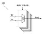
체배비 제어기(130)는 체배비 선택 신호에 응답하여 지연 고정 루프(110)에서 출력되는 8개의 다중 위상 클록(D1-D8)에서 T/8 또는 T/4의 지연시간을 갖는 클럭 쌍을 선택한다. 체배비 제어기(130)는, 도 5에 도시된 바와 같이, 체배비 선택 신호에 응답하여 전압 제어 지연선(118)의 다중 위상 클록(Di, Dbi, 1≤i≤8)을 선택 출력하는 먹스부로 구성된다.The
예를 들어, 체배비가 4인 경우, 체배된 클럭은 8개의 다중 위상 클록(D1-D8)의 상승 에지에서 클락을 트리거시켜 얻는다. 즉, 도 6a에 도시된 바와 같이, 8개의 다중 위상 클락(D1-D8)을 2개씩 짝지어 T/8 지속 시간을 갖는 클럭 펄스 4개를 발생시키고, 이 4개의 펄스를 조합하여 최종적으로 체배된 클럭 신호(fmul_x4)을 얻을 수 있다. 예를 들어, 체배비가 2인 경우, 도 6b에 도시된 바와 같이, 8개의 다중 위상 클록 중 T/4 의 위상차를 갖는 4개의 클록만을 사용하여, T/4 지속 시간을 갖는 클럭 펄스 2개를 발생시키고, 이 2개의 펄스를 조합하여 2배 체배된 클럭 신호(fmul_x2)를 발생한다.For example, if the multiplication ratio is 4, the multiplied clock is obtained by triggering a clock on the rising edges of the eight multi-phase clocks D1-D8. That is, as shown in FIG. 6A, eight multi-phase clocks D1-D8 are paired in two to generate four clock pulses having a T / 8 duration, and the four pulses are combined to finally multiply. The clock signal fmul_x4 can be obtained. For example, if the multiplication ratio is 2, as shown in Fig. 6B, using only four clocks having a phase difference of T / 4 out of eight multi-phase clocks, two clock pulses having a T / 4 duration are used. Is generated, and the two pulses are combined to generate a doubled clock signal fmul_x2.
한편, 2배 또는 4배 체배된 클럭 신호들은 기준 클락 신호(fref)과 위상 차이가 존재한다. 이 위상 차이를 보상하기 위해, 또 하나의 전압 제어 지연선을 사 용할 수 있다. 추가되는 전압 제어 지연선은 일반적인 지연 고정 루프의 제어 방법과 동일한 방법으로 제어 전압을 조절한다. 다만, 위상 검출기의 두 입력 클럭의 주파수가 다르므로, 도 7과 같이, 인에이블 신호(enable)를 위상 검출기에 연결하고 인에이블 신호가 활성화된 경우에만 위상 검출기가 동작하도록 설계할 수 있다. 인에이블 신호(enable)의 지속 시간은 체배비가 4인 경우 T/4(fmul_x4'), 체배비가 2인 경우 T/2(fmul_x2')로 설계하여, 인에이블 신호(enable)가 로직 하이인 동안에 체배된 클락의 상승 에지가 한 번만 오도록 설계할 수 있다.On the other hand, the clock signals multiplied by 2 or 4 times have a phase difference from the reference clock signal fref. To compensate for this phase difference, another voltage controlled delay line can be used. The added voltage control delay line adjusts the control voltage in the same way as the control method of a general delay lock loop. However, since the frequencies of the two input clocks of the phase detector are different, as shown in FIG. 7, an enable signal is connected to the phase detector and the phase detector may be designed to operate only when the enable signal is activated. The duration of the enable signal (enable) is T / 4 (fmul_x4 ') when the multiplication ratio is 4, and T / 2 (fmul_x2') when the multiplication ratio is 2 so that the enable signal (enable) is logic high. It can be designed so that the rising edge of the multiplied clock comes only once during the.
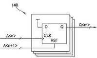
도 8은 도 1의 펄스 생성기를 설명하는 블락 다이어그램이다. 도 8을 참조하면, 펄스 생성기(140)는 8개의 다중 위상 클락(A<n>, n=1~8)을 입력으로 받아 체배된 클락의 반주기에 해당하는 지속 시간을 갖는 펄스들(Q<m>, m=1~4)을 발생한다. 펄스 생성기(140)는 이전 클럭 신호(A<n>)에 응답하여 전원전압(Vcc)에 연결된 데이터를 래치하고, 현재 클럭 신호(A<n+1>)에 리셋되는 D-플립플롭으로 구성된다.FIG. 8 is a block diagram illustrating the pulse generator of FIG. 1. Referring to FIG. 8, the
도 9는 도 8의 D-플립플롭을 구체적으로 설명하는 회로 다이어그램이다. 도 9를 참조하면, D-플립플롭은 전원 전압(Vcc)과 접지 전압(Vss) 사이에 직렬 연결되는 제1 및 제2 피모스 트랜지스터들(P1, P2)과 제1 엔모스 트랜지스터(N1), 그리고 제3 피모스 트랜지스터(P3)와 제2 및 제3 엔모스 트랜지스터들(N2, N3)을 포함한다. 제1 피모스 트랜지스터(P1)와 제1 엔모스 트랜지스터(N1)의 게이트들은 리셋 신호(RST)에 연결되고, 제2 피모스 트랜지스터(P2)와 제2 엔모스 트랜지스터(N2)의 게이트들은 클럭 신호(CLK)에 연결된다. 제3 피모스 트랜지스터(P3)와 제3 엔모스 트랜지스터(N3)의 게이트들은 제2 피모스 트랜지스터(P2)와 제1 엔모스 트랜지스터(N1)의 드레인(A)에 연결된다. 그리고, D-플립플롭은 제3 피모스 트랜지스터(P3)와 제2 엔모스 트랜지스터(N2)의 드레인(B)이 그 입력 단자에 연결되는 인버터(INV)를 더 포함한다.FIG. 9 is a circuit diagram illustrating the D-flip-flop of FIG. 8 in detail. Referring to FIG. 9, the D-flip-flop includes first and second PMOS transistors P1 and P2 and first NMOS transistor N1 connected in series between a power supply voltage Vcc and a ground voltage Vss. And a third PMOS transistor P3 and second and third NMOS transistors N2 and N3. Gates of the first PMOS transistor P1 and the first NMOS transistor N1 are connected to the reset signal RST, and gates of the second PMOS transistor P2 and the second NMOS transistor N2 are clocked. Is connected to the signal CLK. Gates of the third PMOS transistor P3 and the third NMOS transistor N3 are connected to the drain A of the second PMOS transistor P2 and the first NMOS transistor N1. The D flip-flop further includes an inverter INV having a drain B of the third PMOS transistor P3 and the second NMOS transistor N2 connected to an input terminal thereof.
D-플립플롭의 동작은 도 10에서 설명된다. D-플립플롭은 클럭 신호(CLK)와 리셋 신호(RST)가 로직 로우일 때, 노드 A가 전원 전압(Vcc)으로 프리차지되고, 노드 B는 플로팅 상태이다. 이 후, 클럭 신호(CLK)의 상승 에지에 응답하여 노드 B는 로직 로우가 되고, 출력 신호(Q)는 로직 하이가 된다. 리셋 신호(RST)의 상승 에지에 응답하여 노드 A는 로직 로우가 되고, 노드 B는 전원 전압(Vcc)가 되고 출력 펄스(Q)는 로직 로우로 리셋된다.The operation of the D-flip-flop is described in FIG. In the D-flip-flop, when the clock signal CLK and the reset signal RST are logic low, the node A is precharged to the power supply voltage Vcc, and the node B is in a floating state. Thereafter, in response to the rising edge of the clock signal CLK, the node B becomes logic low and the output signal Q becomes logic high. In response to the rising edge of the reset signal RST, node A becomes logic low, node B becomes power supply voltage Vcc, and output pulse Q is reset to logic low.
도 11은 도 1의 펄스 조합기(150)를 설명하는 회로 다이어그램이다. 도 11을 참조하면, 펄스 조합기(150)는 제1 내지 제4 출력 펄스들(Q<m>, m=1,2,3,4)을 입력하는 제1 내지 제4 인버터들(1101~1104), 제1 및 제2 인버터들(1101, 1102)의 출력을 입력하는 제1 낸드 게이트(1105), 제3 및 제4 인버터들(1103, 1104)의 출력을 입력하는 제2 낸드 게이트(1106), 제1 낸드 게이트(1105)의 출력을 입력하는 제5 인버터(1107), 제2 낸드 게이트(1106)의 출력을 입력하는 제6 인버터(1108), 그리고 제5 및 제6 인버터들(1107, 1108)의 출력을 입력하여 체배된 클럭 신호(fmul)를 출력하는 제3 낸드 게이트(1109)를 포함한다. 체배된 클럭 신호(fmul)는 기준 클럭 신호(fref)와 동기화되고, 듀티비 50%를 갖는다. 그리고 체배된 클럭 신호(fmul)는전압 제어 지연선(118)에서 N 개의 다중 위상 클락들을 생성했을 때 최대 체배비가 N/2 로 한정된다.FIG. 11 is a circuit diagram illustrating the
따라서, 주파수 체배기(100)는 지연 고정 루프를 기반으로 하기 때문에, 위상 고정 루프 기반의 주파수 체배기와 비교하였을 때 지터 축적 현상이 나타나지 않는다. 그리고, 주파수 체배기(100)는 1차 특성식을 갖기 때문에 넓은 주파수 범위에 대해 안정적으로 동작하며, 고속 동작이 가능하다.Therefore, since the frequency multiplier 100 is based on a delay locked loop, there is no jitter accumulation phenomenon when compared to a frequency multiplier based on a phase locked loop. In addition, since the frequency multiplier 100 has a first characteristic formula, the frequency multiplier 100 operates stably over a wide frequency range and enables high speed operation.
본 발명은 도면에 도시된 일 실시예를 참고로 설명되었으나 이는 예시적인 것에 불과하며, 본 기술 분야의 통상의 지식을 가진 자라면 이로부터 다양한 변형 및 균등한 타 실시예가 가능하다는 점을 이해할 것이다. 따라서, 본 발명의 진정한 기술적 보호 범위는 첨부된 등록청구범위의 기술적 사상에 의해 정해져야 할 것이다.Although the present invention has been described with reference to one embodiment shown in the drawings, this is merely exemplary, and those skilled in the art will understand that various modifications and equivalent other embodiments are possible therefrom. Therefore, the true technical protection scope of the present invention will be defined by the technical spirit of the appended claims.
상술한 본 발명의 주파수 체배기에 의하면, 지연 고정 루프를 기반으로 하여 지터 축적 현상이 나타나지 않고, 1차 특성식을 갖기 때문에 넓은 주파수 범위에 대해 안정적으로 동작하며, 고속 동작 또한 가능하다.According to the frequency multiplier of the present invention described above, the jitter accumulation phenomenon does not appear based on the delay locked loop, and since it has a first-order characteristic equation, it stably operates over a wide frequency range and also enables high-speed operation.
Claims (11)
Translated fromKoreanPriority Applications (1)
| Application Number | Priority Date | Filing Date | Title |
|---|---|---|---|
| KR1020050134338AKR100853862B1 (en) | 2005-12-29 | 2005-12-29 | Delay-Locked Loop-Based Frequency Multiplier |
Applications Claiming Priority (1)
| Application Number | Priority Date | Filing Date | Title |
|---|---|---|---|
| KR1020050134338AKR100853862B1 (en) | 2005-12-29 | 2005-12-29 | Delay-Locked Loop-Based Frequency Multiplier |
Publications (2)
| Publication Number | Publication Date |
|---|---|
| KR20070071142A KR20070071142A (en) | 2007-07-04 |
| KR100853862B1true KR100853862B1 (en) | 2008-08-26 |
Family
ID=38506332
Family Applications (1)
| Application Number | Title | Priority Date | Filing Date |
|---|---|---|---|
| KR1020050134338AExpired - Fee RelatedKR100853862B1 (en) | 2005-12-29 | 2005-12-29 | Delay-Locked Loop-Based Frequency Multiplier |
Country Status (1)
| Country | Link |
|---|---|
| KR (1) | KR100853862B1 (en) |
Cited By (2)
| Publication number | Priority date | Publication date | Assignee | Title |
|---|---|---|---|---|
| KR100983485B1 (en) | 2008-07-17 | 2010-09-27 | 고려대학교 산학협력단 | Frequency Multiplication System Based on Delayed Fixed Loop and Its Multiplication Method |
| KR101013920B1 (en) | 2008-07-30 | 2011-02-14 | 고려대학교 산학협력단 | Frequency multiplication system and its control method |
Families Citing this family (2)
| Publication number | Priority date | Publication date | Assignee | Title |
|---|---|---|---|---|
| KR100792379B1 (en)* | 2006-09-29 | 2008-01-09 | 주식회사 하이닉스반도체 | Frequency division method of delay locked loop and delay locked loop capable of operating at various frequencies. |
| KR101208026B1 (en)* | 2011-02-08 | 2012-12-04 | 연세대학교 산학협력단 | Edge combiner, frequency multiplier and method of frequency multiplying using the edge combiner |
Citations (4)
| Publication number | Priority date | Publication date | Assignee | Title |
|---|---|---|---|---|
| KR970077989A (en)* | 1996-05-08 | 1997-12-12 | 문정환 | Frequency synthesizer |
| KR20040046323A (en)* | 2002-11-27 | 2004-06-05 | 주식회사 하이닉스반도체 | Dll circuit |
| KR20050048838A (en)* | 2003-11-20 | 2005-05-25 | 주식회사 하이닉스반도체 | Delay locked loop and its control method |
| KR20050060279A (en)* | 2003-12-16 | 2005-06-22 | 세원텔레텍 주식회사 | 2nd order frequency doubler and design method thereof |
- 2005
- 2005-12-29KRKR1020050134338Apatent/KR100853862B1/ennot_activeExpired - Fee Related
Patent Citations (4)
| Publication number | Priority date | Publication date | Assignee | Title |
|---|---|---|---|---|
| KR970077989A (en)* | 1996-05-08 | 1997-12-12 | 문정환 | Frequency synthesizer |
| KR20040046323A (en)* | 2002-11-27 | 2004-06-05 | 주식회사 하이닉스반도체 | Dll circuit |
| KR20050048838A (en)* | 2003-11-20 | 2005-05-25 | 주식회사 하이닉스반도체 | Delay locked loop and its control method |
| KR20050060279A (en)* | 2003-12-16 | 2005-06-22 | 세원텔레텍 주식회사 | 2nd order frequency doubler and design method thereof |
Cited By (2)
| Publication number | Priority date | Publication date | Assignee | Title |
|---|---|---|---|---|
| KR100983485B1 (en) | 2008-07-17 | 2010-09-27 | 고려대학교 산학협력단 | Frequency Multiplication System Based on Delayed Fixed Loop and Its Multiplication Method |
| KR101013920B1 (en) | 2008-07-30 | 2011-02-14 | 고려대학교 산학협력단 | Frequency multiplication system and its control method |
Also Published As
| Publication number | Publication date |
|---|---|
| KR20070071142A (en) | 2007-07-04 |
Similar Documents
| Publication | Publication Date | Title |
|---|---|---|
| KR100861919B1 (en) | Multiphase signal generator and its method | |
| US6784707B2 (en) | Delay locked loop clock generator | |
| US8232844B2 (en) | Synchronous oscillator, clock recovery apparatus, clock distribution circuit, and multi-mode injection circuit | |
| US6292040B1 (en) | Internal clock signal generating circuit having function of generating internal clock signals which are multiplication of an external clock signal | |
| KR100789408B1 (en) | Delay locked loops circuits and method of generating multiplied clock thereof | |
| US20060001496A1 (en) | Array oscillator and polyphase clock generator | |
| KR100644127B1 (en) | Dual loop DL based on voltage controlled delay line with infinite phase shift | |
| KR100980405B1 (en) | DLD circuit | |
| US20030218490A1 (en) | Circuit and method for generating internal clock signal | |
| CN103718460B (en) | Apparatus and system for digital phase interpolator with improved linearity | |
| KR100507875B1 (en) | Clock Divider in Delay Locked Loop and its method | |
| US6366150B1 (en) | Digital delay line | |
| JP2001217694A (en) | Delay-adjusting circuit and clock-generating circuit using same | |
| US7952413B2 (en) | Clock generating circuit and clock generating method thereof | |
| KR100663329B1 (en) | Frequency multiplier | |
| US20070165476A1 (en) | Clock signal generating circuit | |
| KR100853862B1 (en) | Delay-Locked Loop-Based Frequency Multiplier | |
| KR101000486B1 (en) | Delay-Locked Loop-Based Frequency Multiplier | |
| JP7255790B2 (en) | semiconductor equipment | |
| KR100878030B1 (en) | Clock Generator with Frequency Lock Based on Delayed Fixed Loop | |
| KR20210069530A (en) | Semiconductor device for adjusting phases of multi-phase signal | |
| KR100693895B1 (en) | Clock Multiplier with Phase-locked Loop Circuit | |
| KR100937716B1 (en) | Delay Fixed Loop Based Frequency Multiplication Apparatus and Method | |
| US9735786B2 (en) | Apparatus and methods for single phase spot circuits | |
| KR20080023496A (en) | Duty ratio control circuit and its method |
Legal Events
| Date | Code | Title | Description |
|---|---|---|---|
| PA0109 | Patent application | St.27 status event code:A-0-1-A10-A12-nap-PA0109 | |
| A201 | Request for examination | ||
| PA0201 | Request for examination | St.27 status event code:A-1-2-D10-D11-exm-PA0201 | |
| PN2301 | Change of applicant | St.27 status event code:A-3-3-R10-R13-asn-PN2301 St.27 status event code:A-3-3-R10-R11-asn-PN2301 | |
| PG1501 | Laying open of application | St.27 status event code:A-1-1-Q10-Q12-nap-PG1501 | |
| E902 | Notification of reason for refusal | ||
| PE0902 | Notice of grounds for rejection | St.27 status event code:A-1-2-D10-D21-exm-PE0902 | |
| R18-X000 | Changes to party contact information recorded | St.27 status event code:A-3-3-R10-R18-oth-X000 | |
| E13-X000 | Pre-grant limitation requested | St.27 status event code:A-2-3-E10-E13-lim-X000 | |
| P11-X000 | Amendment of application requested | St.27 status event code:A-2-2-P10-P11-nap-X000 | |
| P13-X000 | Application amended | St.27 status event code:A-2-2-P10-P13-nap-X000 | |
| E701 | Decision to grant or registration of patent right | ||
| PE0701 | Decision of registration | St.27 status event code:A-1-2-D10-D22-exm-PE0701 | |
| GRNT | Written decision to grant | ||
| PR0701 | Registration of establishment | St.27 status event code:A-2-4-F10-F11-exm-PR0701 | |
| PR1002 | Payment of registration fee | St.27 status event code:A-2-2-U10-U11-oth-PR1002 Fee payment year number:1 | |
| PG1601 | Publication of registration | St.27 status event code:A-4-4-Q10-Q13-nap-PG1601 | |
| PN2301 | Change of applicant | St.27 status event code:A-5-5-R10-R13-asn-PN2301 St.27 status event code:A-5-5-R10-R11-asn-PN2301 | |
| R18-X000 | Changes to party contact information recorded | St.27 status event code:A-5-5-R10-R18-oth-X000 | |
| FPAY | Annual fee payment | Payment date:20110615 Year of fee payment:4 | |
| PR1001 | Payment of annual fee | St.27 status event code:A-4-4-U10-U11-oth-PR1001 Fee payment year number:4 | |
| FPAY | Annual fee payment | Payment date:20120615 Year of fee payment:5 | |
| PR1001 | Payment of annual fee | St.27 status event code:A-4-4-U10-U11-oth-PR1001 Fee payment year number:5 | |
| LAPS | Lapse due to unpaid annual fee | ||
| PC1903 | Unpaid annual fee | St.27 status event code:A-4-4-U10-U13-oth-PC1903 Not in force date:20130819 Payment event data comment text:Termination Category : DEFAULT_OF_REGISTRATION_FEE | |
| R18-X000 | Changes to party contact information recorded | St.27 status event code:A-5-5-R10-R18-oth-X000 | |
| R18-X000 | Changes to party contact information recorded | St.27 status event code:A-5-5-R10-R18-oth-X000 | |
| PC1903 | Unpaid annual fee | St.27 status event code:N-4-6-H10-H13-oth-PC1903 Ip right cessation event data comment text:Termination Category : DEFAULT_OF_REGISTRATION_FEE Not in force date:20130819 | |
| P22-X000 | Classification modified | St.27 status event code:A-4-4-P10-P22-nap-X000 | |
| P22-X000 | Classification modified | St.27 status event code:A-4-4-P10-P22-nap-X000 | |
| R18-X000 | Changes to party contact information recorded | St.27 status event code:A-5-5-R10-R18-oth-X000 |