KR100851403B1 - Light emitting device and method for manufacturing light emitting device - Google Patents
Light emitting device and method for manufacturing light emitting deviceDownload PDFInfo
- Publication number
- KR100851403B1 KR100851403B1KR1020060072176AKR20060072176AKR100851403B1KR 100851403 B1KR100851403 B1KR 100851403B1KR 1020060072176 AKR1020060072176 AKR 1020060072176AKR 20060072176 AKR20060072176 AKR 20060072176AKR 100851403 B1KR100851403 B1KR 100851403B1
- Authority
- KR
- South Korea
- Prior art keywords
- light emitting
- substrate
- recess
- receiving substrate
- protruding portion
- Prior art date
- Legal status (The legal status is an assumption and is not a legal conclusion. Google has not performed a legal analysis and makes no representation as to the accuracy of the status listed.)
- Expired - Fee Related
Links
Images


Classifications
- H—ELECTRICITY
- H10—SEMICONDUCTOR DEVICES; ELECTRIC SOLID-STATE DEVICES NOT OTHERWISE PROVIDED FOR
- H10H—INORGANIC LIGHT-EMITTING SEMICONDUCTOR DEVICES HAVING POTENTIAL BARRIERS
- H10H20/00—Individual inorganic light-emitting semiconductor devices having potential barriers, e.g. light-emitting diodes [LED]
- H10H20/01—Manufacture or treatment
- H10H20/011—Manufacture or treatment of bodies, e.g. forming semiconductor layers
- H10H20/018—Bonding of wafers
- H—ELECTRICITY
- H10—SEMICONDUCTOR DEVICES; ELECTRIC SOLID-STATE DEVICES NOT OTHERWISE PROVIDED FOR
- H10H—INORGANIC LIGHT-EMITTING SEMICONDUCTOR DEVICES HAVING POTENTIAL BARRIERS
- H10H20/00—Individual inorganic light-emitting semiconductor devices having potential barriers, e.g. light-emitting diodes [LED]
- H10H20/80—Constructional details
- H10H20/85—Packages
- H10H20/852—Encapsulations
- H10H20/853—Encapsulations characterised by their shape
Landscapes
- Led Devices (AREA)
- Led Device Packages (AREA)
Abstract
Translated fromKoreanDescription
Translated fromKorean도 1은 본 발명의 제1 실시예에 따른 발광 소자를 설명하기 위한 단면도이다.1 is a cross-sectional view for describing a light emitting device according to a first embodiment of the present invention.
도 2 내지 도 9는 도1의 발광 소자의 제조과정 및 발광 소자를 설명하기 위하여 발광부 제조과정을 순차적으로 도시한 단면도들이다.2 through 9 are cross-sectional views sequentially illustrating a manufacturing process of the light emitting device of FIG. 1 and a manufacturing process of the light emitting part.
도 10 내지 도 12는 본 발명의 제1 실시예에 따른 수용 기판의 제조 과정을 설명하기 위한 단면도들이다.10 to 12 are cross-sectional views illustrating a manufacturing process of an accommodating substrate according to a first exemplary embodiment of the present invention.
도 13 내지 도 16은 발광부를 수용 기판에 안착시키고 다이싱하여 발광 소자를 제조하는 과정을 설명하기 위한 단면도들이다.13 to 16 are cross-sectional views illustrating a process of manufacturing a light emitting device by mounting and dicing a light emitting unit on a receiving substrate.
도 17은 본 발명의 제2 실시예에 따른 발광 소자의 제조방법 및 발광 소자를 설명하기 위한 정면도이다.17 is a front view illustrating a method of manufacturing a light emitting device and a light emitting device according to a second embodiment of the present invention.
도 18은 본 발명의 제3 실시예에 따른 발광 소자를 설명하기 위한 발광 소자의 단면도이다.18 is a cross-sectional view of a light emitting device for explaining a light emitting device according to a third embodiment of the present invention.
도 19은 본 발명의 제3 실시예에 따른 발광부의 확대 사시도이다.19 is an enlarged perspective view of a light emitting unit according to a third exemplary embodiment of the present invention.
<도면의 주요 부분에 대한 부호의 설명><Explanation of symbols for the main parts of the drawings>
100:발광 소자110:발광부100: light emitting element 110: light emitting unit
111:페시베이션112:밀러 패턴111: Passivation 112: Miller pattern
120:에피택시층121:N형 반도체층120: epitaxy layer 121: N-type semiconductor layer
122:활성층123:P형 반도체층122: active layer 123: P-type semiconductor layer
130:발광 패턴131:N형 반도체 패턴130: light emitting pattern 131: N-type semiconductor pattern
132:활성 패턴133:P형 반도체 패턴132: active pattern 133: P-type semiconductor pattern
210:수용 기판220:리셉터 기판210: accommodating substrate 220: receptor substrate
222:리세스222: recess
본 발명은 발광 소자의 제조방법 및 발광 소자에 관한 것이다. 보다 자세하게는, 본 발명은 높은 품질을 유지하면서 대량으로 제조할 수 있으며, 제조 비용도 현저하게 줄일 수가 있는 발광 소자의 제조방법 및 발광 소자를 제공하는 것이다.The present invention relates to a method of manufacturing a light emitting device and a light emitting device. More specifically, the present invention provides a method of manufacturing a light emitting device and a light emitting device which can be manufactured in large quantities while maintaining high quality and can significantly reduce manufacturing costs.
백열전구가 발명된 이래, 백열전구는 조명 시장의 많은 부분을 점유하고 있다. 하지만, 백열전구는 자동차 브레이크등, 교통신호등과 같이 단색광만이 필요한 부분에서도 필터를 이용하여 필요한 색깔을 얻어내고 있어, 불필요한 색깔들은 낭비하게 되어 에너지 효율을 크게 떨어뜨린다.Since incandescent bulbs have been invented, incandescent bulbs have occupied a large part of the lighting market. However, incandescent bulbs are used to obtain the required color even in areas where only monochromatic light is required, such as automobile brake lights and traffic lights, which wastes unnecessary colors and greatly reduces energy efficiency.
그러나, 1960년대 도입된 발광 다이오드(LED)는 필요한 단색광만을 만들어 내기 때문에 불필요한 낭비를 없애고 에너지 효율을 높일 수 있다. 얼마 전까지도 발광 다이오드(LED)의 주된 사용 용도는 표시등이나 일부 디스플레이 영역에 국한되었으나, 최근 유기금속화학기상증착법(MOCVD, Metal Organic Chemical Vapor Deposition)으로 성장한 고효율의 AlGaInP(적색) 및 GaInN(녹색) 발광 다이오드(LED)의 개발로 발광 다이오드는 그 영역을 넓혀 자동차의 내부 조명 및 브레이크등, 교통신호등, 총천연색 디스플레이 옥외 전광판 및 휴대폰/PDA의 백라이트 조명등과 같은 넓은 분야에서 사용되고 있다.However, since the light emitting diode (LED) introduced in the 1960s generates only required monochromatic light, unnecessary waste and energy efficiency can be improved. Until recently, the main use of light emitting diodes (LEDs) was limited to indicators and some display areas. With the development of light emitting diodes (LEDs), light emitting diodes have broadened their scope and are used in a wide range of fields such as automobile interior lights and brake lights, traffic signals, full color display outdoor billboards, and backlight lights of mobile phones / PDAs.
따라서, 발광 다이오드의 대량생산이 요구되고 있으나, 현재까지 발광 다이오드의 대량 생산 및 생산 과정에서 여러 가지 어려움이 있는 실정이다.Therefore, mass production of light emitting diodes is required, but there are various difficulties in mass production and production processes of light emitting diodes.
구체적으로, 발광 다이오드를 제작하는 과정에서 단결정의 성장 기판으로부터 형성시킨 화합물 반도체를 분리해 낼 때에 화합물 반도체 및 성장 기판과의 격자 결함 및 열 팽창 계수의 차이 등과 같은 요인에 의해서 화합물 반도체에 크랙이 발생할 수 있으며, 이에 따라 생산효율이 저하될 수 있다.Specifically, when the compound semiconductor formed from the single crystal growth substrate is separated in the process of manufacturing a light emitting diode, cracks may occur in the compound semiconductor due to factors such as lattice defects and thermal expansion coefficient differences between the compound semiconductor and the growth substrate. In this way, the production efficiency may be reduced.
예를 들면, 일반적으로 질화갈륨(GaN)기판은 사파이어(Al2O3) 기판을 성장 기판으로 사용하여 제조할 수 있다. 그러나, 질화갈륨과 사파이어는 격자 상수 및 열팽창 계수의 차이로 인하여, 사파이어 기판에 질화갈륨층을 형성하게 되면, 고 밀도의 결정성 결함이 발생할 수 있다. 따라서, 질화갈륨층을 사파이어 기판으로부터 분리해내는 과정에서 질화갈륨층에 크랙이 발생하여, 질화갈륨층의 생산 효율이 떨어지며, 제품의 질이 떨어질 수 있다.For example, a gallium nitride (GaN) substrate is generally manufactured by using a sapphire (Al 2 O 3) substrate as a growth substrate. However, gallium nitride and sapphire due to the difference in lattice constant and coefficient of thermal expansion, if the gallium nitride layer is formed on the sapphire substrate, high density crystalline defects may occur. Therefore, cracks may occur in the gallium nitride layer in the process of separating the gallium nitride layer from the sapphire substrate, thereby lowering the production efficiency of the gallium nitride layer and lowering the quality of the product.
최근에는 사파이어 기판 위에 질화갈륨층을 성장시킨 후에, 투명한 사파이어 기판에 레이저를 조사하여, 질화갈륨층과 사파이어 기판의 계면부분을 녹이는 레이 저 리프트 오프(Laser lift off)공정으로 사파이어 기판에 형성된 질화갈륨층을 분리하는 방식을 취하고 있다. 그러나, 이러한 레이저 리프트 오프 공정으로 분리된 질화갈륨층은 매우 얇아서 다루기가 어려우며 상술한 바와 같이 사파이어 및 질화갈륨의 열팽창 계수 및 격자 상수의 차이에 의해서 분리하는 과정에서 비교적 얇은 질화갈륨층이 쉽게 깨질 수가 있다. 따라서, 질화갈륨층의 분리과정에서 발생하는 크랙은 질화갈륨의 대량 생산 및 생산 비용면에서 불리하며, 생산 효율이 저하시키고 있는 실정이다.In recent years, after growing a gallium nitride layer on a sapphire substrate, a laser is irradiated to a transparent sapphire substrate, and a gallium nitride formed on the sapphire substrate by a laser lift off process that melts the interface between the gallium nitride layer and the sapphire substrate. It takes a way to separate the layers. However, the gallium nitride layer separated by the laser lift-off process is very thin and difficult to handle, and as described above, the relatively thin gallium nitride layer cannot be easily broken in the separation process due to the difference in thermal expansion coefficient and lattice constant of sapphire and gallium nitride. have. Therefore, cracks generated in the gallium nitride layer separation process are disadvantageous in terms of mass production and production cost of gallium nitride, and production efficiency is deteriorated.
본 발명은 상술한 문제점을 해결하기 위한 것으로서, 본 발명의 일 목적은 제조가 용이하며 우수한 품질의 발광 소자를 제조할 수 있는 발광 소자의 제조방법 및 발광 소자를 제공하는 것이다.SUMMARY OF THE INVENTION The present invention has been made to solve the above problems, and an object of the present invention is to provide a method of manufacturing a light emitting device and a light emitting device which can manufacture a light emitting device of easy quality and excellent quality.
본 발명의 다른 목적은 제조가 신속하고 용이하여 대량생산에 유리하고, 제조 비용이 저렴하여 제품 단가를 낮출 수 있는 발광 소자의 제조방법 및 발광 소자를 제공하는 것이다.Another object of the present invention is to provide a method of manufacturing a light emitting device and a light emitting device which can be quickly and easily manufactured, which is advantageous for mass production, and low in manufacturing cost, thereby lowering the product cost.
본 발명의 또 다른 목적은 모재와 모재로부터 성장시킨 발광부를 분리해 내는 단계에서 불량을 줄일 수 있는 발광 소자의 제조방법 및 발광 소자를 제공하는 것이다.Still another object of the present invention is to provide a method of manufacturing a light emitting device and a light emitting device capable of reducing defects in a step of separating the light emitting part grown from the base material and the base material.
본 발명의 또 다른 목적은 다양한 빛을 조사할 수 있는 발광 소자의 제조방법 및 발광 소자를 제공하는 것이다.Still another object of the present invention is to provide a method of manufacturing a light emitting device capable of irradiating various lights and a light emitting device.
상술한 본 발명의 목적들을 달성하기 위한 본 발명의 바람직한 실시예에 따르면, 발광 소자의 제조 방법은 성장 기판 상에 돌출 부위를 구비한 독립된 복수개의 발광부를 형성하는 단계, 발광부를 성장 기판으로부터 분리하는 단계, 상기 돌출 부위의 형상에 대응하는 리세스가 형성된 수용 기판에 상기 발광부를 안착시키는 단계 및 발광부가 안착된 수용 기판을 발광 단위로 다이싱하는 단계를 구비한다.According to a preferred embodiment of the present invention for achieving the above object of the present invention, the manufacturing method of the light emitting device comprises the steps of forming a plurality of independent light emitting portion having a projecting portion on the growth substrate, separating the light emitting portion from the growth substrate And mounting the light emitting part on a receiving substrate having a recess corresponding to the shape of the protruding portion, and dicing the receiving substrate on which the light emitting part is seated in a light emitting unit.
먼저, 성장 기판 상에 복수개의 발광부를 형성하는 단계에서 발광부는 성장 기판으로부터 성장되며, 성장 기판은 단결정(single crystal)으로 형성된 기판을 사용한다.First, in the step of forming a plurality of light emitting portions on the growth substrate, the light emitting portions are grown from the growth substrate, and the growth substrate uses a substrate formed of a single crystal.
일반적으로 결정은 단결정, 다결정 및 비정질로 구분되며, 단결정에서 전자의 움직임이 가장 원활하다. 발광부를 제조하기 위해서 성장 기판으로 단결정 기판을 사용한다. 이때, 단결정 기판은 GaN, MgO, Si, 사파이어 등과 같이 다양한 기판을 사용할 수 있으며, 최근에는 GaN화합물 반도체를 형성하기 위한 기판으로 사파이어를 많이 사용하고 있다.Generally, crystals are divided into single crystal, polycrystalline and amorphous, and electron movement is most smooth in single crystal. In order to manufacture a light emitting part, a single crystal substrate is used as a growth substrate. In this case, various substrates such as GaN, MgO, Si, and sapphire may be used as the single crystal substrate, and recently, sapphire is used as a substrate for forming GaN compound semiconductors.
발광부를 형성시키기 위해서 먼저, 단결정 기판 상에 n형 반도체층, 활성층 및 p형 반도체층을 포함하는 에피택시층을 형성시킬 수 있다.In order to form the light emitting part, an epitaxial layer including an n-type semiconductor layer, an active layer and a p-type semiconductor layer may be first formed on a single crystal substrate.
성장 기판 상에 에피택시층을 형성시킨 후에, 성장 기판의 표면상에서 에피택시층을 소정의 크기로 아이솔레이션(isolation)하여 독립된 다수개의 발광 패턴을 제공할 수 있다. 이때, 발광부는 에피택시층이 아이솔레이션되어 독립된 n형 반도체 패턴, 활성 패턴 및 p형 반도체 패턴을 포함한다.After the epitaxy layer is formed on the growth substrate, the epitaxial layer may be isolated to a predetermined size on the surface of the growth substrate to provide a plurality of independent light emitting patterns. In this case, the light emitting unit includes an independent n-type semiconductor pattern, an active pattern, and a p-type semiconductor pattern with the epitaxial layer is isolated.
발광부를 성장기판으로부터 형성시킨 후에 발광부를 성장 기판으로부터 분리 하는 단계는 레이저를 조사하여 분리하거나 화학적인 방법을 사용하여 분리할 수 있다. 에피택시층을 성장 기판으로부터 아이솔레이션하여 다수개의 발광 패턴을 제공한 후에, 크기가 300마이크로 미터 이하의 작은 발광부 단위로 분리하기 때문에 성장 기판으로부터 발광 패턴을 분리해 낼 때에 발생하는 발광 패턴의 크랙을 최소화할 수 있다.After the light emitting part is formed from the growth substrate, the step of separating the light emitting part from the growth substrate may be separated by irradiating a laser or using a chemical method. After the epitaxy layer is isolated from the growth substrate to provide a plurality of light emission patterns, the light emission pattern crack generated when the light emission pattern is separated from the growth substrate is separated by a small light emitting unit having a size of 300 micrometers or less. It can be minimized.
상술한 방법에 의해서 성장기판으로부터 분리된 발광부는 수용 기판에 안착시키는 단계를 거친다. 이때, 발광부를 수용 기판에 안착시키기 위하여 발광부는 돌출 부위를 포함할 수 있으며, 수용 기판에는 상기 돌출 부위의 형상에 대응하는 리세스가 형성될 수 있다.The light emitting portion separated from the growth substrate by the above-described method is subjected to the step of seating on the receiving substrate. In this case, the light emitting part may include a protruding portion to seat the light emitting portion on the receiving substrate, and a recess corresponding to the shape of the protruding portion may be formed in the receiving substrate.
수용 기판은 먼저 리셉터 기판을 제공하고, 상기 돌출 부위에 대응하는 리세스를 형성하여 제공할 수 있으며, 수용 기판을 형성하는 일 예로, 리셉터 기판 상에 상기 돌출 부위에 대응하는 부분을 제외하고 마스크 패턴을 형성한 후에 리셉터 기판을 식각하여 돌출 부위의 형상에 대응하는 리세스를 형성할 수 있다. 그리고, 마스크 패턴을 제거하는 과정을 거쳐 수용 기판을 완성할 수 있다.The receiving substrate may first provide a receptor substrate, and may form and provide a recess corresponding to the protruding portion. For example, the receiving substrate may include a mask pattern except for a portion corresponding to the protruding portion on the receptor substrate. After forming the substrate, the receptor substrate may be etched to form a recess corresponding to the shape of the protruding portion. The receiving substrate may be completed by removing the mask pattern.
따라서, 상기 발광부들은 발광부를 수용 기판에 안착시키는 단계에서 상기 돌출 부위의 형상에 대응하는 리세스에 안착될 수 있다. 이때, 돌출 부위를 포함하는 복수개의 발광부를 유동 상태로 제공하여, 돌출 부위에 대응하는 리세스를 포함하는 수용 기판 상에 발광부를 안착시킬 수가 있다. 또한, 돌출 부위는 미리 정해진 몇몇 형상들 중 선택된 하나의 형상으로 제공될 수 있으며, 돌출 부위에 대응하여 리세스도 정해진 몇몇 형상들 중 선택된 하나의 형상으로 제공될 수 있다. 예를 들어, 하나의 수용기판에 사각형, 원형, T-자형, L-자형 등과 같이 모두 동일하지 않은 리세스를 형성할 수 있으며, 발광부의 돌출 부위를 각 리세스에 삽입될 수 있는 형상으로 형성할 수가 있다. 따라서 돌출 부위를 이용하여 발광부를 리세스에 안착시킬 때, 설계자가 원하는 배치에 따라 발광부를 수용기판 상에 배치시킬 수가 있다. 이를 이용하여 RGB 색상에 따른 각각의 발광부를 수용기판에 원하는 위치에 선택적으로 안착시킬 수 있다.Therefore, the light emitting parts may be seated in a recess corresponding to the shape of the protruding portion in the step of mounting the light emitting part on the receiving substrate. At this time, the plurality of light emitting parts including the protruding portions may be provided in a flow state to seat the light emitting portions on the receiving substrate including recesses corresponding to the protruding portions. In addition, the protruding portion may be provided in a shape selected from one of several predetermined shapes, and the recess may also be provided in the selected one of several predetermined shapes corresponding to the protruding portion. For example, not all recesses may be formed in one receiving substrate such as a rectangle, a circle, a T-shape, or an L-shape, and a protruding portion of the light emitting part may be formed into a shape that can be inserted into each recess. You can do it. Therefore, when the light emitting portion is seated in the recess using the protruding portion, the light emitting portion can be disposed on the receiving substrate according to the arrangement desired by the designer. By using this, each light emitting unit according to the RGB color may be selectively seated at a desired position on the receiving substrate.
이때, 돌출 부위는 발광부를 리세스가 형성된 수용 기판에 안착시키기 위한 하나의 방법이며, 경우에 따라서는 다른 물리적 수단을 사용할 수 있으며, 서로 인력이 작용할 수 있는 화학적 또는 전기적 방법을 사용하여 발광부 및 수용 기판을 결합 시킬 수도 있다.In this case, the protruding portion is one method for seating the light emitting portion on the recessed receiving substrate, and in some cases, other physical means may be used, and the light emitting portion and the chemical or electrical method may be attracted to each other. The receiving substrate can also be bonded.
발광부를 수용 기판에 안착시킨 후에 발광부가 안착된 상기 수용 기판을 발광 단위로 다이싱하여 발광 소자를 완성할 수 있다. 발광 단위는 제작자의 의도에 따라 하나 또는 그 이상의 발광부를 포함할 수 있다.After mounting the light emitting unit on the receiving substrate, the receiving substrate on which the light emitting unit is seated may be diced into light emitting units to complete the light emitting device. The light emitting unit may include one or more light emitting units according to the manufacturer's intention.
상술한 제조방법으로 제조되는 발광 소자는 발광부 및 수용 기판을 구비한다. 발광부는 발광부의 일면으로부터 돌출된 돌출 부위를 포함하며, 수용 기판은 리셉터 기판 및 리셉터 기판에 돌출 부위에 대응하여 형성된 리세스를 포함한다. 그리고, 발광 소자는 리세스에 돌출 부위를 접합하고, 수용 기판을 발광 단위로 절단하여 형성된다.The light emitting device manufactured by the above-described manufacturing method includes a light emitting portion and a receiving substrate. The light emitting part includes a protruding portion protruding from one surface of the light emitting portion, and the receiving substrate includes a receptor substrate and a recess formed in the receptor substrate corresponding to the protruding portion. The light emitting element is formed by bonding a protruding portion to the recess and cutting the receiving substrate into light emitting units.
다만, 돌출 부위는 발광부를 리세스가 형성된 수용 기판에 안착시키기 위한 하나의 방법이며, 경우에 따라서는 다른 물리적 수단을 사용할 수 있으며, 서로 인 력이 작용할 수 있는 화학적 또는 전기적 방법을 사용하여 발광부 및 수용 기판을 결합 시킬 수도 있다.However, the protruding portion is one method for seating the light emitting part on the recessed receiving substrate, and in some cases, other physical means may be used, and the light emitting part may be formed using a chemical or electrical method in which humans may act. And a receiving substrate.
또한, 발광부를 수용 기판에 안착시킨 후에 발광부가 안착된 상기 수용 기판을 발광 단위로 다이싱하여 발광 소자를 완성할 수 있다. 발광 단위는 제작자의 의도에 따라 하나 또는 그 이상의 발광부를 포함할 수 있다.In addition, the light emitting unit may be completed by mounting the light emitting unit on the receiving substrate and dicing the receiving substrate on which the light emitting unit is mounted in a light emitting unit. The light emitting unit may include one or more light emitting units according to the manufacturer's intention.
이하 첨부된 도면들을 참조하여 본 발명의 바람직한 실시예를 상세하게 설명하지만, 본 발명이 실시예에 의해 제한되거나 한정되는 것은 아니다.Hereinafter, preferred embodiments of the present invention will be described in detail with reference to the accompanying drawings, but the present invention is not limited or limited by the embodiments.
실시예1Example 1
도 1은 본 발명의 제1 실시예에 따른 발광 소자를 설명하기 위한 단면도이다.1 is a cross-sectional view for describing a light emitting device according to a first embodiment of the present invention.
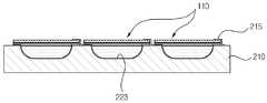
도 1을 참조하면, 발광 소자(100)는 발광부(110) 및 수용 기판(210)을 구비한다. 발광부(110)는 발광부(110)의 일면으로부터 돌출된 돌출 부위(140)를 포함하며, 수용 기판(210)은 리셉터 기판(220) 및 리셉터 기판(220)에 돌출 부위(140)에 대응하여 형성된 리세스(222)를 포함한다. 그리고, 발광 소자(100)는 리세스(222)에 돌출 부위(140)를 접합하고, 수용 기판(210)을 발광 단위로 절단하여 형성된다.Referring to FIG. 1, the
이때, 돌출 부위(140)는 발광부(110)를 리세스(222)가 형성된 수용 기판(210)에 안착시키기 위한 하나의 방법이며, 경우에 따라서는 다른 물리적 수단을 사용할 수 있으며, 서로 인력이 작용할 수 있는 화학적 또는 전기적 방법을 사용하 여 발광부 및 수용 기판을 결합 시킬 수도 있다.At this time, the protruding
또한, 돌출 부위(140)를 형성하는 재료로는 Cr, Ti, Cu, Ni, Au, Ag, Sn, PnSn, AuSn, SnAgCu 및 CuAg 중의 하나 또는 조합을 사용하거나 합금으로 제공할 수 있다. 돌출 부위(140) 또는 리세스(222) 상의 전극 패턴(223) 또는 둘 다는 솔더링을 할 수 있는 재료로 형성되며, 후술하는 바와 같이 돌출 부위(140)를 리세스(222)에 안착시킨 후, 열을 가하여 돌출 부위(140)와 리세스(222) 상의 전극 패턴(223)을 접합시킬 수가 있다.In addition, as the material for forming the protruding
그리고, 발광부(110)를 수용 기판(210)에 안착시킨 후에 발광부(110)가 안착된 상기 수용 기판(210)을 발광 단위로 다이싱(dicing)하여 발광 소자(100)를 완성할 수 있다. 본 실시예에서는 발광 소자(100)의 발광 단위가 하나의 발광부(110)를 포함하지만, 제작자의 의도에 따라서 두개, 세개 또는 그 이상의 발광부를 포함하도록 수용 기판을 다이싱하여 다양한 숫자의 발광부를 포함하는 발광 단위를 갖는 발광 소자를 제공할 수 있다.After the
본 발명에 따른 발광 소자의 제조 방법은 성장 기판 상에 복수개의 발광부를 형성하는 단계, 발광부를 성장 기판으로부터 분리하는 단계, 발광부를 수용 기판에 안착시키는 단계 및 발광부가 안착된 수용 기판을 발광 단위로 다이싱하는 단계를 구비한다.A method of manufacturing a light emitting device according to the present invention comprises the steps of forming a plurality of light emitting portions on a growth substrate, separating the light emitting portion from the growth substrate, mounting the light emitting portion on the receiving substrate and the receiving substrate on which the light emitting portion is mounted as a light emitting unit Dicing.
이하, 발광부의 제조방법을 상세하게 설명한다.Hereinafter, the manufacturing method of a light emitting part is demonstrated in detail.
도 2 내지 도 9는 도1의 발광 소자의 제조과정 및 발광 소자를 설명하기 위하여 발광부 제조과정을 순차적으로 도시한 단면도들이다.2 through 9 are cross-sectional views sequentially illustrating a manufacturing process of the light emitting device of FIG. 1 and a manufacturing process of the light emitting part.
도 2 내지 도 9를 참조하면, 발광부(110)는 발광 패턴(130) 및 돌출 부위(140)를 포함한다.2 to 9, the
성장 기판(10) 상에 복수개의 발광부(110)를 형성하는 단계에서 발광 부(110)는 성장 기판(10)으로부터 성장되며, 성장 기판(10)은 단결정(single crystal)으로 형성된 기판을 사용한다.In the forming of the plurality of
일반적으로 결정은 단결정, 다결정 및 비정질로 구분되며, 단결정에서 전자의 움직임이 가장 원활하며, 발광부(110)를 제조하기 위해서 성장 기판으로 단결정 기판을 사용한다. 이때, 단결정 기판은 GaN, MgO, Si, 사파이어 등과 같이 다양한 기판을 사용할 수 있으며, 최근에는 GaN화합물 반도체를 형성하기 위한 기판으로 사파이어를 많이 사용하고 있다.Generally, crystals are classified into single crystals, polycrystals, and amorphous materials, and electron movement is most smooth in single crystals, and a single crystal substrate is used as a growth substrate to manufacture the
도 2에 도시된 바와 같이, 발광부(110)를 형성시키기 위해서 먼저 성장 기판(10) 상에 순차적으로 n형 반도체층(121), 활성층(122) 및 p형 반도체층(123)을 포함하는 에피택시층(120)을 형성시킬 수 있다.As shown in FIG. 2, in order to form the
그리고, 도 3에 도시된 바와 같이, 성장 기판(10) 상에 에피택시층(120)을 형성시킨 후에는 성장 기판(10)의 표면상에서 에피택시층(120)을 소정의 크기로 아이솔레이션(isolation)하여 독립된 다수개의 발광 패턴(130)을 제공한다.3, after the
따라서, 발광부(110)는 에피택시층(120)이 아이솔레이션되어 독립된 n형 반도체 패턴(131), 활성 패턴(132) 및 p형 반도체 패턴(133)을 포함한다. 그리고, 원하는 크기의 발광 패턴(130)을 형성한 후에는 발광 패턴(130)의 가장자리를 산화물 계열로 페시베이션(111)을 형성할 수 있다. 이때, 발광 패턴(130)의 상부 표면 이 일부 노출되도록 한다.Accordingly, the
그리고, 도 4에 도시된 바와 같이, 발광 패턴(130) 및 페시베이션(111)을 형성한 후에 페시베이션(111)이 형성되지 않은 노출된 발광 패턴(130)의 상부 표면에 빛의 반사를 위한 밀러 패턴(112)을 형성한다. 밀러 패턴(112)은 도금(plating) 또는 증착(deposition)하여 형성할 수 있으며, 밀러 패턴(112)을 형성시킨 후에는 밀러 패턴(112)상에 상부 전극 패턴(115)을 형성한다. 상부 전극 패턴(115)은 P-메탈 전극을 사용한다.As shown in FIG. 4, after the
그리고, 도 5에 도시된 바와 같이, 상부 전극 패턴(115)을 제외한 밀러 패턴(112) 주변에는 마스크 패턴(113)을 형성한다. 본 실시예에서 마스크 패턴(113)은 PR(photoresist)코팅을 사용할 수 있다. 마스크 패턴(113)을 형성하고 나서, 도 6에 도시된 바와 같이, 발광 패턴(130)의 상부에 돌출 부위(140)를 형성한다.As shown in FIG. 5, the
PR(photoresist)이란 특정 파장대의 빛에 노출되면 반응을 하는 감광 고분자 화합물(photosensitive polymer)이며, 반응은 PR의 일정 부분이 노광될 때 노광된 부분의 폴리머(polymer) 사슬이 끊어지거나 혹은 더 강하게 결합하는 것을 의미한다. 일반적으로 노광된 부분의 polymer 결합사슬이 끊어지는 PR을 positive PR이라 하며 그 반대의 경우를 negative PR이라 한다. 본 실시예에서는 도 7에 도시된 바와 같이, 마스크 패턴(113)을 positive PR을 사용하여 돌출 부위(140)를 형성한 후에 PR(Photoresist)코팅 즉, 마스크 패턴(113)을 제거할 수 있다.Photoresist (PR) is a photosensitive polymer that reacts when exposed to light in a specific wavelength range, and the reaction occurs when the polymer chain in the exposed portion breaks or bonds more strongly when a portion of the PR is exposed. I mean. In general, the PR that breaks the exposed polymer bond chain is called a positive PR and vice versa. In this embodiment, as shown in FIG. 7, after forming the protruding
그리고, 상술한 바와 같이 형성된 다수개의 발광부(110)들을 성장기판(10)으로부터 분리한다. 도 8은 성장기판(10)으로부터 분리된 낱개의 발광부(110)가 도 시되며, 도 9는 낱개의 발광부(110)의 사시도이다.Then, the plurality of
발광부(110)를 성장기판(10)으로부터 형성시킨 후에 발광부(110)를 성장 기판(10)으로부터 분리하는 단계는 레이저를 조사하여 분리하거나 화학적인 방법을 사용하여 분리할 수 있다. 따라서, 본 발명에 따른 발광부(110)는 에피택시층(120)을 성장 기판(10)으로부터 아이솔레이션하여 다수개의 발광 패턴(130)을 형성하고 밀러 패턴(112), 상부 전극 패턴(115) 및 페시베이션(111) 등을 형성하여 발광부(110)를 완성한 후에, 미세한 크기의 발광부(110) 상태로 분리하기 때문에 종래에 커다란 웨이퍼 상태에서 절단하여 낱개의 발광부를 생산하는 경우에 비하여, 성장 기판(10)으로부터 발광부(110)를 분리해 낼 때에 발생하는 발광부(110)의 크랙을 최소화할 수 있다.After the
이하, 발광부가 안착되는 수용 기판의 제조방법을 상세하게 설명한다.Hereinafter, the manufacturing method of the accommodating substrate on which the light emitting part is seated will be described in detail.
도 10 내지 도 12는 본 발명의 제1 실시예에 따른 수용 기판의 제조 과정을 설명하기 위한 단면도들이다.10 to 12 are cross-sectional views illustrating a manufacturing process of an accommodating substrate according to a first exemplary embodiment of the present invention.
도 10 내지 도 12를 참조하면, 수용 기판(210)을 제공하기 위하여 먼저, 도 10에 도시된 바와 같이 평탄한 리셉터 기판(220)을 제공하고, 리셉터 기판(220) 상에 상술한 발광부(110)의 돌출 부위(140)에 대응하는 부분을 제외하고 마스크층(211)을 형성한다. 본 실시예에서 마스크층(211)은 상술한 마스크 패턴(113)과 동일한 PR(Photoresist)코팅을 사용할 수 있으며, 마스크층(211)을 형성하고 나서, 도 11에 도시된 바와 같이, 리셉터 기판(220)의 상부에 상술한 돌출 부위(140)의 형상에 대응하는 리세스(222)를 형성한다. 그리고, 도 12에 도시된 바와 같이 마 스크층(211)을 제거하여 수용 기판(210)을 완성할 수 있다. 그리고, 리세스(222)의 표면에는 전달 전극 패턴(223)을 형성한다. 참고로, 전달 전극 패턴(223)을 형성하는 재료로는 Zn, Ni, Ag, Cu, Ti, Pt, Au, Sn, PbSn, AuSn, SnAgCu 및 CuAg 등의 금속 중의 하나를 사용하거나 합금으로 제공할 수 있다.10 to 12, in order to provide the receiving
이하, 상술한 방법으로 제조한 발광부 및 수용 기판을 사용하여, 발광부를 수용 기판에 안착시키는 과정을 상세하게 설명한다.Hereinafter, the process of mounting the light emitting part on the receiving substrate using the light emitting part and the receiving substrate manufactured by the above-described method will be described in detail.
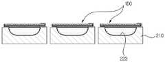
도 13 내지 도 16은 발광부를 수용 기판에 안착시키고 다이싱하여 발광 소자를 제조하는 과정을 설명하기 위한 단면도들이다.13 to 16 are cross-sectional views illustrating a process of manufacturing a light emitting device by mounting and dicing a light emitting unit on a receiving substrate.
도 13 내지 도 16을 참조하면, 발광부(110)에 형성된 돌출 부위(140)가 수용 기판(210) 상에 형성된 리세스(222)에 안착된다.13 to 16, the protruding
발광부(110)를 수용 기판(210)에 안착시키는 단계에서 발광부(110)들은 발광부(110)에 형성된 돌출 부위(140)의 형상에 대응하는 리세스(222)에 안착될 수 있다. 이때, 도 13에 도시된 바와 같이, 돌출 부위(140)를 포함하는 복수개의 발광부(110)를 유동 상태로 제공하여, 돌출 부위(140)에 대응하는 리세스(222)를 포함하는 수용 기판(210) 상에 발광부(110)를 안착시킬 수가 있다.In the step of mounting the
또한, 본 실시예에서 돌출 부위(140)는 동일한 형상으로 제공되지만, 본 발명의 다른 실시예에서는 돌출 부위를 정해진 소정의 형상들 중 하나로 제공하고, 발광부들은 돌출 부위들이 각각 대응하는 리세스에서만 안착되도록 함으로써 소정의 배치에 맞게 자동으로 안착될 수 있다.In addition, in the present embodiment, the protruding
이때, 돌출 부위는 발광부를 리세스가 형성된 수용 기판에 안착시키기 위한 하나의 방법이며, 경우에 따라서는 다른 물리적 수단을 사용할 수 있으며, 서로 인력이 작용할 수 있는 화학적 또는 전기적 방법을 사용하여 발광부 및 수용 기판을 결합 시킬 수도 있다.In this case, the protruding portion is one method for seating the light emitting portion on the recessed receiving substrate, and in some cases, other physical means may be used, and the light emitting portion and the chemical or electrical method may be attracted to each other. The receiving substrate can also be bonded.
그리고, 도 14에 도시된 바와 같이, 발광부를 수용기판에 안착시킨 후, 열을 가해 돌출 부위(140)와 리세스(222)를 서로 접합할 수가 있다. 돌출 부위(140) 또는 전극패턴(223) 또는 둘 다는 일종의 솔더부로서 PnSn, AuSn, SnAgCu 및 CuAg로 구성될 수 있으며, 돌출 부위(140)는 열에 의해 N-메탈 전극과 일체로 접합될 수 있다.As shown in FIG. 14, after the light emitting unit is seated on the receiving substrate, heat may be applied to bond the protruding
그리고, 도 15에 도시된 바와 같이, 수용 기판 상에 안착된 발광부(110)에는 하부 전극 패턴(215)을 형성한다. 이때, 하부 전극 패턴(215)은 N-메탈 전극을 사용한다. 참고로, 하부 전극 패턴(215)은 금속 또는 투명전극(ITO)를 사용할 수 있다. 투명 전극은 일반적으로 도전성 및 투광성을 갖는 ITO(Indium Tin Oxide) 또는 IZO(Indium Zinc Oxide)을 사용할 수 있다.As shown in FIG. 15, a
그리고, 도 16에 도시된 바와 같이, 발광부(110)를 수용 기판(210)에 안착시킨 후에 발광부(110)가 안착된 수용 기판(210)을 발광 단위로 다이싱하여 발광 소자(100)를 완성할 수 있다. 본 실시예에서 발광 소자(100)의 발광 단위가 하나의 발광부(110)를 포함하지만, 제작자의 의도에 따라서 두개, 세개 또는 그 이상의 발광부를 포함하도록 수용 기판을 다이싱하여 다양한 숫자의 발광부를 포함하는 발광 단위를 갖는 발광 소자를 제공할 수 있다.As shown in FIG. 16, the
실시예2Example 2
도 17은 본 발명의 제2 실시예에 따른 발광 소자의 제조방법 및 발광 소자를 설명하기 위한 정면도이다.17 is a front view illustrating a method of manufacturing a light emitting device and a light emitting device according to a second embodiment of the present invention.
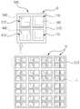
도 17을 참조하면, 제2 실시예에 따른 발광 소자는 다른 형상의 돌출 부위를 구비하는 발광부(110, 310, 410) 및 수용 기판(510)을 포함한다.Referring to FIG. 17, the light emitting device according to the second embodiment includes
제2 실시예에 따른 발광 소자(500)는 발광부가 네개가 포함된 발광 단위(U)를 갖는다. 구체적으로, 두개의 발광부(110)는 제1 실시예의 발광부(110)와 동일하며, 다른 두개의 발광부(310, 410)는 각각 제1 실시예의 발광부(110)와 다른 L-형 및 T-형상의 돌출 부위(310, 440)를 구비한다. 다만, L-형 및 T-형상의 돌출 부위(310, 440)를 갖는 발광부(310, 410)들도 제1 실시예의 발광부(110)의 제조방법 및 발광부와 실질적으로 동일하다. 따라서, 발광부(310, 410)들의 구체적인 제조방법 및 발광부에 대한 설명은 제1 실시예의 발광부(110)의 제조방법 및 발광부에 대한 설명 및 도면을 참조할 수 있으며, 반복되는 내용은 생략될 수 있다.The
먼저, 각기 다른 형상의 돌출 부위를 구비하는 발광부(110, 310, 410)들을 유동 상태로 제공하여 발광부(110, 310, 410)들을 수용 기판에 안착시킨 후에 발광부(110, 310, 410)들이 안착된 상기 수용 기판(510)을 절개선(L)을 따라 발광 단위(U)로 다이싱하여 발광 소자(500)를 완성할 수 있다. 발광 단위는 제작자의 의도에 따라 하나 또는 그 이상의 발광부를 포함할 수 있으나, 본 실시예에서는 네개의 발광부(110, 310, 410)를 갖는 발광 단위(U)를 제공하기 위하여 절개선(L)을 따라 절개된다.First, the
발광부(110, 310, 410)들이 각기 다른 돌출 부위(140, 340, 440)를 구비하여 발광부(110, 310, 410)들은 발광부(110, 310, 410)들이 구비하는 돌출 부위(140, 340, 440)의 형상에 대응하는 리세스에 안착될 수 있다.The
이때, 돌출 부위는 발광부를 리세스가 형성된 수용 기판에 안착시키기 위한 하나의 방법이며, 경우에 따라서는 다른 물리적 수단을 사용할 수 있으며, 서로 인력이 작용할 수 있는 화학적 또는 전기적 방법을 사용하여 발광부 및 수용 기판을 결합 시킬 수도 있다.In this case, the protruding portion is one method for seating the light emitting portion on the recessed receiving substrate, and in some cases, other physical means may be used, and the light emitting portion and the chemical or electrical method may be attracted to each other. The receiving substrate can also be bonded.
발광부(110, 310, 410)들을 수용 기판에 안착시킨 후에 발광부(110, 310, 410)들이 안착된 상기 수용 기판(510)을 발광 단위(U)로 다이싱하여 발광 소자(500)를 완성할 수 있다. 발광 단위는 제작자의 의도에 따라 하나 또는 그 이상의 발광부를 포함할 수 있다.After mounting the
따라서, 종래에 단색광으로만 사용되던 발광 소자가 다양한 색을 낼 수 있다. 구체적으로, 적색 발광 다이오드(LED)의 제작을 위해 사용되는 GaP, GaAsP, AlGaAs, AlGaInP 등을 사용하여 발광 패턴을 형성한 후에, L-형상의 돌출 부위(340)를 갖는 발광부(310)를 형성하고, 황색 발광 다이오드(LED)의 제작을 위해 사용되는 GaP, AlGaInP, InGaN 등을 사용하여 발광 패턴을 형성한 후에, T-형상의 돌출 부위(440)를 갖는 발광부(410)를 형성할 수 있다. 그리고, 청색 발광 다이오드(LED)의 제작을 위한 물질계로는 실리콘카바이드(SiC)와 같은 IV족, ZnSe 및 ZnS와 같은 II-VI족, GaN계의 III-V족 반도체 등이 있으나, 최근에는 주로 GaN 물질계를 사용한다. 따라서, 상술한 물질계를 사용하여 발광 패턴을 형성하며, 제1 실시예와 같은 사각형의 돌출부위를 구비하는 발광부(110)를 형성할 수 있다. 이때, 도 19에 도시된 바와 같이 각기 다른 돌출 부위를 갖는 발광부들이 수용 기판(510)에 형성된 리세스 중에서 대응하는 형상의 리세스에 안착된다. 그리고, 제작자가 원하는 발광 단위로 절개하여 발광 소자를 완성할 수 있다.Therefore, the light emitting device conventionally used only for monochromatic light can produce various colors. Specifically, after forming a light emitting pattern using GaP, GaAsP, AlGaAs, AlGaInP, etc. used for manufacturing a red light emitting diode (LED), the
실시예3Example 3
도 18은 본 발명의 제3 실시예에 따른 발광 소자를 설명하기 위한 발광 소자의 단면도이며, 도 19는 본 발명의 제3 실시예에 따른 발광부의 확대 사시도이다.18 is a cross-sectional view of a light emitting device for explaining a light emitting device according to a third embodiment of the present invention, and FIG. 19 is an enlarged perspective view of a light emitting unit according to a third embodiment of the present invention.
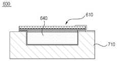
도 18 및 도 19를 참조하면, 제3 실시예에 따른 발광 소자(600)는 발광부(610) 및 수용 기판(710)을 구비한다. 발광부(610)는 발광부(610)의 일면으로부터 돌출된 돌출 부위(640)를 포함하며, 수용 기판(710)은 리셉터 기판 및 리셉터 기판에 돌출 부위(640)에 대응하여 형성된 리세스를 포함한다. 그리고, 발광 소자(600)는 리세스에 돌출 부위(640)를 접합하고, 수용 기판(710)을 발광 단위로 절단하여 형성된다.18 and 19, the
제3 실시예에 따른 발광 소자의 제조방법 및 발광 소자는 제 1 실시예의 발광 소자의 제조방법 및 발광 소자와 실질적으로 동일하다. 따라서 제3 실시예에서 발광 소자의 제조방법 및 발광 소자에 대한 설명은 제1 실시예의 발광 소자의 제조방법 및 발광 소자에 대한 설명 및 도면을 참조할 수 있으며, 반복되는 내용은 생략될 수 있다.The manufacturing method and the light emitting device according to the third embodiment are substantially the same as the manufacturing method and the light emitting device of the first embodiment. Therefore, the method of manufacturing the light emitting device and the description of the light emitting device in the third embodiment may be referred to the description and drawings of the method of manufacturing the light emitting device and the light emitting device of the first embodiment, and the repeated content may be omitted.
다만, 본 발명의 제3 실시예에서는 발광부에 형성된 돌출 부위의 형상이 제1 실시예의 돌출 부위와 다르게 형성된다. 이를 위해서, 돌출 부위를 형성할 때 PR층을 원하는 돌출 부위의 두께보다 두껍게 형성하고, PR층에서 돌출 부위를 거의 사각 기둥 형상으로 형성할 수가 있다. 또한, 사각 기둥 형상의 돌출 부위에 대응하도록 리세스를 이방성 식각으로 에칭하여 사각 기둥에 대응하는 리세스 형상을 만들 수가 있다.However, in the third embodiment of the present invention, the shape of the protruding portion formed in the light emitting portion is formed differently from the protruding portion of the first embodiment. For this purpose, when forming the protruding portion, the PR layer can be formed thicker than the thickness of the desired protruding portion, and the protruding portion can be formed in a substantially rectangular columnar shape in the PR layer. In addition, the recess may be etched by anisotropic etching so as to correspond to the protruding portion of the rectangular pillar shape, thereby forming a recess shape corresponding to the rectangular pillar.
본 발명의 발광 소자의 제조방법 및 그 제조방법으로 만든 발광 소자는 제조가 용이하며 우수한 품질의 발광 소자를 제조할 수 있다.The manufacturing method of the light emitting element of this invention and the light emitting element made by the manufacturing method are easy to manufacture, and can manufacture the light emitting element of excellent quality.
또한, 본 발명의 발광 소자의 제조방법 및 그 제조방법으로 만든 발광 소자는 발광부를 개별적으로 수용 기판에 접합하는 것이 아니라, 동시에 많은 발광부를 수용 기판에 접합하여 제조가 신속하고 용이하여 대량생산에 유리하고, 제조 비용이 저렴하여 제품 단가를 낮출 수 있다.In addition, the manufacturing method of the light emitting device of the present invention and the light emitting device made by the manufacturing method are not suitable for mass production because the light emitting parts are not individually bonded to the receiving substrate, but at the same time, many light emitting parts are bonded to the receiving substrate. In addition, the manufacturing cost is low, it is possible to lower the product cost.
또한, 본 발명에 따른 발광 소자의 제조방법 및 그 제조방법으로 만든 발광 소자는 성장 기판과 성장 기판으로부터 성장시킨 발광부를 분리해 내는 단계에서 불량을 줄일 수 있다.In addition, the manufacturing method of the light emitting device according to the present invention and the light emitting device made by the manufacturing method can reduce the defect in the step of separating the growth substrate and the light emitting portion grown from the growth substrate.
또한, 본 발명에 따른 발광 소자의 제조방법 및 그 제조방법으로 만든 발광 소자는 다양한 발광부를 갖는 발광 단위로 제공하기 때문에 다양한 빛을 조사할 수 있다.In addition, the method of manufacturing the light emitting device according to the present invention and the light emitting device made by the method of manufacturing the light emitting device having various light emitting parts can be irradiated with various light.
또한, 작은 크기의 발광부를 수용 기판에 조립하게 되므로, 방열 성능이 우수한 효과가 있다.In addition, since the light emitting unit having a small size is assembled to the receiving substrate, the heat dissipation performance is excellent.
상술한 바와 같이, 본 발명의 바람직한 실시예를 참조하여 설명하였지만 해당 기술분야의 숙련된 당업자라면 하기의 청구범위에 기재된 본 발명의 사상 및 영역으로부터 벗어나지 않는 범위 내에서 본 발명을 다양하게 수정 및 변경시킬 수 있음을 이해할 수 있을 것이다.As described above, although described with reference to the preferred embodiment of the present invention, those skilled in the art various modifications and variations of the present invention without departing from the spirit and scope of the invention described in the claims below I can understand that you can.
Claims (19)
Translated fromKoreanPriority Applications (2)
| Application Number | Priority Date | Filing Date | Title |
|---|---|---|---|
| KR1020060072176AKR100851403B1 (en) | 2006-07-31 | 2006-07-31 | Light emitting device and method for manufacturing light emitting device |
| US11/599,391US8013349B2 (en) | 2006-07-31 | 2006-11-15 | Light emitting device and method of manufacturing the same |
Applications Claiming Priority (1)
| Application Number | Priority Date | Filing Date | Title |
|---|---|---|---|
| KR1020060072176AKR100851403B1 (en) | 2006-07-31 | 2006-07-31 | Light emitting device and method for manufacturing light emitting device |
Publications (2)
| Publication Number | Publication Date |
|---|---|
| KR20080011771A KR20080011771A (en) | 2008-02-11 |
| KR100851403B1true KR100851403B1 (en) | 2008-08-08 |
Family
ID=38985261
Family Applications (1)
| Application Number | Title | Priority Date | Filing Date |
|---|---|---|---|
| KR1020060072176AExpired - Fee RelatedKR100851403B1 (en) | 2006-07-31 | 2006-07-31 | Light emitting device and method for manufacturing light emitting device |
Country Status (2)
| Country | Link |
|---|---|
| US (1) | US8013349B2 (en) |
| KR (1) | KR100851403B1 (en) |
Families Citing this family (7)
| Publication number | Priority date | Publication date | Assignee | Title |
|---|---|---|---|---|
| KR101092063B1 (en)* | 2009-04-28 | 2011-12-12 | 엘지이노텍 주식회사 | Light emitting device package and method for fabricating the same |
| US8907362B2 (en) | 2012-01-24 | 2014-12-09 | Cooledge Lighting Inc. | Light-emitting dies incorporating wavelength-conversion materials and related methods |
| WO2013112435A1 (en) | 2012-01-24 | 2013-08-01 | Cooledge Lighting Inc. | Light - emitting devices having discrete phosphor chips and fabrication methods |
| US8896010B2 (en) | 2012-01-24 | 2014-11-25 | Cooledge Lighting Inc. | Wafer-level flip chip device packages and related methods |
| TWI631697B (en)* | 2012-02-17 | 2018-08-01 | 財團法人工業技術研究院 | Light-emitting element and method of manufacturing same |
| US9343443B2 (en) | 2014-02-05 | 2016-05-17 | Cooledge Lighting, Inc. | Light-emitting dies incorporating wavelength-conversion materials and related methods |
| US12394648B2 (en)* | 2021-03-02 | 2025-08-19 | Samsung Electronics Co., Ltd. | Display transfer structure including light emitting elements and transferring method of light emitting elements |
Citations (2)
| Publication number | Priority date | Publication date | Assignee | Title |
|---|---|---|---|---|
| KR20040013394A (en)* | 2002-08-06 | 2004-02-14 | 주식회사 옵토웨이퍼테크 | A Light Emitting Diode and A Method for Manufacturing thereof |
| KR20050013989A (en)* | 2002-04-09 | 2005-02-05 | 오리올 인코포레이티드 | A method of fabricating vertical devices using a metal support film |
Family Cites Families (8)
| Publication number | Priority date | Publication date | Assignee | Title |
|---|---|---|---|---|
| KR19980069992A (en)* | 1997-01-20 | 1998-10-26 | 사와무라시코우 | Method for mounting a compound unit of an optical semiconductor device and a support substrate and an optical semiconductor device on a support substrate |
| KR20010079490A (en) | 1999-12-09 | 2001-08-22 | 구자홍 | 3-5 Group semiconductor device |
| TW525278B (en)* | 2001-03-15 | 2003-03-21 | Opto Tech Corp | Package structure of high-efficiency electro-optical device and the forming method thereof |
| JP2004119620A (en)* | 2002-09-25 | 2004-04-15 | Matsushita Electric Ind Co Ltd | Semiconductor device and manufacturing method thereof |
| JP2005079551A (en) | 2003-09-03 | 2005-03-24 | Toyoda Gosei Co Ltd | A composite substrate for forming a semiconductor light emitting device, a method for manufacturing the same, and a method for manufacturing a semiconductor light emitting device. |
| KR100613272B1 (en) | 2003-12-30 | 2006-08-18 | 주식회사 이츠웰 | Light emitting diode having vertical electrode structure and manufacturing method thereof |
| KR100667508B1 (en) | 2004-11-08 | 2007-01-10 | 엘지전자 주식회사 | Light emitting device and manufacturing method thereof |
| KR100849788B1 (en) | 2005-06-30 | 2008-07-31 | 삼성전기주식회사 | Manufacturing method of vertical light emitting device |
- 2006
- 2006-07-31KRKR1020060072176Apatent/KR100851403B1/ennot_activeExpired - Fee Related
- 2006-11-15USUS11/599,391patent/US8013349B2/enactiveActive
Patent Citations (2)
| Publication number | Priority date | Publication date | Assignee | Title |
|---|---|---|---|---|
| KR20050013989A (en)* | 2002-04-09 | 2005-02-05 | 오리올 인코포레이티드 | A method of fabricating vertical devices using a metal support film |
| KR20040013394A (en)* | 2002-08-06 | 2004-02-14 | 주식회사 옵토웨이퍼테크 | A Light Emitting Diode and A Method for Manufacturing thereof |
Also Published As
| Publication number | Publication date |
|---|---|
| US20080023687A1 (en) | 2008-01-31 |
| US8013349B2 (en) | 2011-09-06 |
| KR20080011771A (en) | 2008-02-11 |
Similar Documents
| Publication | Publication Date | Title |
|---|---|---|
| EP1798781B1 (en) | LED having vertical structure and method for fabricating the same | |
| CN102347411B (en) | Light emitting device, light emitting device package comprising same and lighting system | |
| TWI663752B (en) | Lighting structure and method of manufactureing a light emitting device | |
| EP2573826B1 (en) | Light emitting device | |
| KR100851403B1 (en) | Light emitting device and method for manufacturing light emitting device | |
| US9093596B2 (en) | Epitaxial wafer for light emitting diode, light emitting diode chip and methods for manufacturing the same | |
| EP2657992A2 (en) | Light emitting device and light emitting device package | |
| US20070145382A1 (en) | Semiconductor light emitting diode and method for manufacturing the same | |
| JPH07273367A (en) | Manufacture of semiconductor substrate and light-emitting device | |
| TWI405354B (en) | Semiconductor structure and light emitting diode | |
| JP2010098068A (en) | Light emitting diode, manufacturing method thereof, and lamp | |
| US20120261686A1 (en) | Light-emitting element and the manufacturing method thereof | |
| KR100889569B1 (en) | Nitride-based light emitting device and its manufacturing method | |
| KR100705225B1 (en) | Manufacturing method of vertical light emitting device | |
| KR100889568B1 (en) | Nitride-based light emitting device and its manufacturing method | |
| KR101316121B1 (en) | Method of fabricating vertical light emitting diode | |
| KR100757802B1 (en) | Vertical Light Emitting Diode and Manufacturing Method Thereof | |
| KR100704872B1 (en) | Vertical Electrode Light Emitting Diode and Manufacturing Method Thereof | |
| KR100663324B1 (en) | Vertical Electrode Light Emitting Diode and Manufacturing Method Thereof | |
| JP4594708B2 (en) | LIGHT EMITTING DIODE AND ITS MANUFACTURING METHOD, LIGHT EMITTING DIODE LAMP | |
| KR100629210B1 (en) | Vertical Light Emitting Diode and Manufacturing Method Thereof | |
| KR101364719B1 (en) | Method of fabricating vertical light emitting diode | |
| US20250006709A1 (en) | Edge-emitting semiconductor devices and related methods | |
| KR101239850B1 (en) | Vertical light emitting diode and method of fabricating the same | |
| TWI423470B (en) | A method of manufacturing a high thermal-dissipation light-emitting element |
Legal Events
| Date | Code | Title | Description |
|---|---|---|---|
| A201 | Request for examination | ||
| PA0109 | Patent application | St.27 status event code:A-0-1-A10-A12-nap-PA0109 | |
| PA0201 | Request for examination | St.27 status event code:A-1-2-D10-D11-exm-PA0201 | |
| E902 | Notification of reason for refusal | ||
| PE0902 | Notice of grounds for rejection | St.27 status event code:A-1-2-D10-D21-exm-PE0902 | |
| P11-X000 | Amendment of application requested | St.27 status event code:A-2-2-P10-P11-nap-X000 | |
| P13-X000 | Application amended | St.27 status event code:A-2-2-P10-P13-nap-X000 | |
| R17-X000 | Change to representative recorded | St.27 status event code:A-3-3-R10-R17-oth-X000 | |
| E902 | Notification of reason for refusal | ||
| PE0902 | Notice of grounds for rejection | St.27 status event code:A-1-2-D10-D21-exm-PE0902 | |
| PG1501 | Laying open of application | St.27 status event code:A-1-1-Q10-Q12-nap-PG1501 | |
| E13-X000 | Pre-grant limitation requested | St.27 status event code:A-2-3-E10-E13-lim-X000 | |
| P11-X000 | Amendment of application requested | St.27 status event code:A-2-2-P10-P11-nap-X000 | |
| P13-X000 | Application amended | St.27 status event code:A-2-2-P10-P13-nap-X000 | |
| E701 | Decision to grant or registration of patent right | ||
| PE0701 | Decision of registration | St.27 status event code:A-1-2-D10-D22-exm-PE0701 | |
| GRNT | Written decision to grant | ||
| PR0701 | Registration of establishment | St.27 status event code:A-2-4-F10-F11-exm-PR0701 | |
| PR1002 | Payment of registration fee | St.27 status event code:A-2-2-U10-U11-oth-PR1002 Fee payment year number:1 | |
| PG1601 | Publication of registration | St.27 status event code:A-4-4-Q10-Q13-nap-PG1601 | |
| P22-X000 | Classification modified | St.27 status event code:A-4-4-P10-P22-nap-X000 | |
| FPAY | Annual fee payment | Payment date:20110711 Year of fee payment:4 | |
| PR1001 | Payment of annual fee | St.27 status event code:A-4-4-U10-U11-oth-PR1001 Fee payment year number:4 | |
| R18-X000 | Changes to party contact information recorded | St.27 status event code:A-5-5-R10-R18-oth-X000 | |
| FPAY | Annual fee payment | Payment date:20120716 Year of fee payment:5 | |
| PR1001 | Payment of annual fee | St.27 status event code:A-4-4-U10-U11-oth-PR1001 Fee payment year number:5 | |
| LAPS | Lapse due to unpaid annual fee | ||
| PC1903 | Unpaid annual fee | St.27 status event code:A-4-4-U10-U13-oth-PC1903 Not in force date:20130805 Payment event data comment text:Termination Category : DEFAULT_OF_REGISTRATION_FEE | |
| PC1903 | Unpaid annual fee | St.27 status event code:N-4-6-H10-H13-oth-PC1903 Ip right cessation event data comment text:Termination Category : DEFAULT_OF_REGISTRATION_FEE Not in force date:20130805 | |
| P22-X000 | Classification modified | St.27 status event code:A-4-4-P10-P22-nap-X000 |