KR100851072B1 - Electronic package and manufacturing method thereof - Google Patents
Electronic package and manufacturing method thereofDownload PDFInfo
- Publication number
- KR100851072B1 KR100851072B1KR1020070020937AKR20070020937AKR100851072B1KR 100851072 B1KR100851072 B1KR 100851072B1KR 1020070020937 AKR1020070020937 AKR 1020070020937AKR 20070020937 AKR20070020937 AKR 20070020937AKR 100851072 B1KR100851072 B1KR 100851072B1
- Authority
- KR
- South Korea
- Prior art keywords
- chip
- pcb
- build
- layer
- insulating material
- Prior art date
- Legal status (The legal status is an assumption and is not a legal conclusion. Google has not performed a legal analysis and makes no representation as to the accuracy of the status listed.)
- Expired - Fee Related
Links
Images


Classifications
- H—ELECTRICITY
- H01—ELECTRIC ELEMENTS
- H01L—SEMICONDUCTOR DEVICES NOT COVERED BY CLASS H10
- H01L24/00—Arrangements for connecting or disconnecting semiconductor or solid-state bodies; Methods or apparatus related thereto
- H01L24/01—Means for bonding being attached to, or being formed on, the surface to be connected, e.g. chip-to-package, die-attach, "first-level" interconnects; Manufacturing methods related thereto
- H01L24/18—High density interconnect [HDI] connectors; Manufacturing methods related thereto
- H01L24/19—Manufacturing methods of high density interconnect preforms
- H—ELECTRICITY
- H01—ELECTRIC ELEMENTS
- H01L—SEMICONDUCTOR DEVICES NOT COVERED BY CLASS H10
- H01L23/00—Details of semiconductor or other solid state devices
- H01L23/12—Mountings, e.g. non-detachable insulating substrates
- H—ELECTRICITY
- H01—ELECTRIC ELEMENTS
- H01L—SEMICONDUCTOR DEVICES NOT COVERED BY CLASS H10
- H01L23/00—Details of semiconductor or other solid state devices
- H01L23/28—Encapsulations, e.g. encapsulating layers, coatings, e.g. for protection
- H—ELECTRICITY
- H01—ELECTRIC ELEMENTS
- H01L—SEMICONDUCTOR DEVICES NOT COVERED BY CLASS H10
- H01L24/00—Arrangements for connecting or disconnecting semiconductor or solid-state bodies; Methods or apparatus related thereto
- H01L24/01—Means for bonding being attached to, or being formed on, the surface to be connected, e.g. chip-to-package, die-attach, "first-level" interconnects; Manufacturing methods related thereto
- H01L24/18—High density interconnect [HDI] connectors; Manufacturing methods related thereto
- H01L24/23—Structure, shape, material or disposition of the high density interconnect connectors after the connecting process
- H01L24/24—Structure, shape, material or disposition of the high density interconnect connectors after the connecting process of an individual high density interconnect connector
- H—ELECTRICITY
- H01—ELECTRIC ELEMENTS
- H01L—SEMICONDUCTOR DEVICES NOT COVERED BY CLASS H10
- H01L24/00—Arrangements for connecting or disconnecting semiconductor or solid-state bodies; Methods or apparatus related thereto
- H01L24/80—Methods for connecting semiconductor or other solid state bodies using means for bonding being attached to, or being formed on, the surface to be connected
- H01L24/83—Methods for connecting semiconductor or other solid state bodies using means for bonding being attached to, or being formed on, the surface to be connected using a layer connector
- H—ELECTRICITY
- H01—ELECTRIC ELEMENTS
- H01L—SEMICONDUCTOR DEVICES NOT COVERED BY CLASS H10
- H01L24/00—Arrangements for connecting or disconnecting semiconductor or solid-state bodies; Methods or apparatus related thereto
- H01L24/93—Batch processes
- H01L24/95—Batch processes at chip-level, i.e. with connecting carried out on a plurality of singulated devices, i.e. on diced chips
- H01L24/97—Batch processes at chip-level, i.e. with connecting carried out on a plurality of singulated devices, i.e. on diced chips the devices being connected to a common substrate, e.g. interposer, said common substrate being separable into individual assemblies after connecting
- H—ELECTRICITY
- H01—ELECTRIC ELEMENTS
- H01L—SEMICONDUCTOR DEVICES NOT COVERED BY CLASS H10
- H01L25/00—Assemblies consisting of a plurality of semiconductor or other solid state devices
- H01L25/03—Assemblies consisting of a plurality of semiconductor or other solid state devices all the devices being of a type provided for in a single subclass of subclasses H10B, H10D, H10F, H10H, H10K or H10N, e.g. assemblies of rectifier diodes
- H01L25/04—Assemblies consisting of a plurality of semiconductor or other solid state devices all the devices being of a type provided for in a single subclass of subclasses H10B, H10D, H10F, H10H, H10K or H10N, e.g. assemblies of rectifier diodes the devices not having separate containers
- H01L25/065—Assemblies consisting of a plurality of semiconductor or other solid state devices all the devices being of a type provided for in a single subclass of subclasses H10B, H10D, H10F, H10H, H10K or H10N, e.g. assemblies of rectifier diodes the devices not having separate containers the devices being of a type provided for in group H10D89/00
- H01L25/0657—Stacked arrangements of devices
- H—ELECTRICITY
- H01—ELECTRIC ELEMENTS
- H01L—SEMICONDUCTOR DEVICES NOT COVERED BY CLASS H10
- H01L2224/00—Indexing scheme for arrangements for connecting or disconnecting semiconductor or solid-state bodies and methods related thereto as covered by H01L24/00
- H01L2224/01—Means for bonding being attached to, or being formed on, the surface to be connected, e.g. chip-to-package, die-attach, "first-level" interconnects; Manufacturing methods related thereto
- H01L2224/02—Bonding areas; Manufacturing methods related thereto
- H01L2224/04—Structure, shape, material or disposition of the bonding areas prior to the connecting process
- H01L2224/04105—Bonding areas formed on an encapsulation of the semiconductor or solid-state body, e.g. bonding areas on chip-scale packages
- H—ELECTRICITY
- H01—ELECTRIC ELEMENTS
- H01L—SEMICONDUCTOR DEVICES NOT COVERED BY CLASS H10
- H01L2224/00—Indexing scheme for arrangements for connecting or disconnecting semiconductor or solid-state bodies and methods related thereto as covered by H01L24/00
- H01L2224/01—Means for bonding being attached to, or being formed on, the surface to be connected, e.g. chip-to-package, die-attach, "first-level" interconnects; Manufacturing methods related thereto
- H01L2224/10—Bump connectors; Manufacturing methods related thereto
- H01L2224/12—Structure, shape, material or disposition of the bump connectors prior to the connecting process
- H01L2224/12105—Bump connectors formed on an encapsulation of the semiconductor or solid-state body, e.g. bumps on chip-scale packages
- H—ELECTRICITY
- H01—ELECTRIC ELEMENTS
- H01L—SEMICONDUCTOR DEVICES NOT COVERED BY CLASS H10
- H01L2224/00—Indexing scheme for arrangements for connecting or disconnecting semiconductor or solid-state bodies and methods related thereto as covered by H01L24/00
- H01L2224/01—Means for bonding being attached to, or being formed on, the surface to be connected, e.g. chip-to-package, die-attach, "first-level" interconnects; Manufacturing methods related thereto
- H01L2224/18—High density interconnect [HDI] connectors; Manufacturing methods related thereto
- H01L2224/20—Structure, shape, material or disposition of high density interconnect preforms
- H01L2224/21—Structure, shape, material or disposition of high density interconnect preforms of an individual HDI interconnect
- H01L2224/211—Disposition
- H—ELECTRICITY
- H01—ELECTRIC ELEMENTS
- H01L—SEMICONDUCTOR DEVICES NOT COVERED BY CLASS H10
- H01L2224/00—Indexing scheme for arrangements for connecting or disconnecting semiconductor or solid-state bodies and methods related thereto as covered by H01L24/00
- H01L2224/01—Means for bonding being attached to, or being formed on, the surface to be connected, e.g. chip-to-package, die-attach, "first-level" interconnects; Manufacturing methods related thereto
- H01L2224/18—High density interconnect [HDI] connectors; Manufacturing methods related thereto
- H01L2224/23—Structure, shape, material or disposition of the high density interconnect connectors after the connecting process
- H01L2224/24—Structure, shape, material or disposition of the high density interconnect connectors after the connecting process of an individual high density interconnect connector
- H01L2224/241—Disposition
- H01L2224/24151—Connecting between a semiconductor or solid-state body and an item not being a semiconductor or solid-state body, e.g. chip-to-substrate, chip-to-passive
- H01L2224/24221—Connecting between a semiconductor or solid-state body and an item not being a semiconductor or solid-state body, e.g. chip-to-substrate, chip-to-passive the body and the item being stacked
- H01L2224/24225—Connecting between a semiconductor or solid-state body and an item not being a semiconductor or solid-state body, e.g. chip-to-substrate, chip-to-passive the body and the item being stacked the item being non-metallic, e.g. insulating substrate with or without metallisation
- H01L2224/24227—Connecting between a semiconductor or solid-state body and an item not being a semiconductor or solid-state body, e.g. chip-to-substrate, chip-to-passive the body and the item being stacked the item being non-metallic, e.g. insulating substrate with or without metallisation the HDI interconnect not connecting to the same level of the item at which the semiconductor or solid-state body is mounted, e.g. the semiconductor or solid-state body being mounted in a cavity or on a protrusion of the item
- H—ELECTRICITY
- H01—ELECTRIC ELEMENTS
- H01L—SEMICONDUCTOR DEVICES NOT COVERED BY CLASS H10
- H01L2224/00—Indexing scheme for arrangements for connecting or disconnecting semiconductor or solid-state bodies and methods related thereto as covered by H01L24/00
- H01L2224/01—Means for bonding being attached to, or being formed on, the surface to be connected, e.g. chip-to-package, die-attach, "first-level" interconnects; Manufacturing methods related thereto
- H01L2224/26—Layer connectors, e.g. plate connectors, solder or adhesive layers; Manufacturing methods related thereto
- H01L2224/31—Structure, shape, material or disposition of the layer connectors after the connecting process
- H01L2224/32—Structure, shape, material or disposition of the layer connectors after the connecting process of an individual layer connector
- H01L2224/321—Disposition
- H01L2224/32151—Disposition the layer connector connecting between a semiconductor or solid-state body and an item not being a semiconductor or solid-state body, e.g. chip-to-substrate, chip-to-passive
- H01L2224/32221—Disposition the layer connector connecting between a semiconductor or solid-state body and an item not being a semiconductor or solid-state body, e.g. chip-to-substrate, chip-to-passive the body and the item being stacked
- H01L2224/32225—Disposition the layer connector connecting between a semiconductor or solid-state body and an item not being a semiconductor or solid-state body, e.g. chip-to-substrate, chip-to-passive the body and the item being stacked the item being non-metallic, e.g. insulating substrate with or without metallisation
- H—ELECTRICITY
- H01—ELECTRIC ELEMENTS
- H01L—SEMICONDUCTOR DEVICES NOT COVERED BY CLASS H10
- H01L2224/00—Indexing scheme for arrangements for connecting or disconnecting semiconductor or solid-state bodies and methods related thereto as covered by H01L24/00
- H01L2224/01—Means for bonding being attached to, or being formed on, the surface to be connected, e.g. chip-to-package, die-attach, "first-level" interconnects; Manufacturing methods related thereto
- H01L2224/42—Wire connectors; Manufacturing methods related thereto
- H01L2224/47—Structure, shape, material or disposition of the wire connectors after the connecting process
- H01L2224/48—Structure, shape, material or disposition of the wire connectors after the connecting process of an individual wire connector
- H01L2224/4805—Shape
- H01L2224/4809—Loop shape
- H01L2224/48091—Arched
- H—ELECTRICITY
- H01—ELECTRIC ELEMENTS
- H01L—SEMICONDUCTOR DEVICES NOT COVERED BY CLASS H10
- H01L2224/00—Indexing scheme for arrangements for connecting or disconnecting semiconductor or solid-state bodies and methods related thereto as covered by H01L24/00
- H01L2224/01—Means for bonding being attached to, or being formed on, the surface to be connected, e.g. chip-to-package, die-attach, "first-level" interconnects; Manufacturing methods related thereto
- H01L2224/42—Wire connectors; Manufacturing methods related thereto
- H01L2224/47—Structure, shape, material or disposition of the wire connectors after the connecting process
- H01L2224/48—Structure, shape, material or disposition of the wire connectors after the connecting process of an individual wire connector
- H01L2224/481—Disposition
- H01L2224/48151—Connecting between a semiconductor or solid-state body and an item not being a semiconductor or solid-state body, e.g. chip-to-substrate, chip-to-passive
- H01L2224/48221—Connecting between a semiconductor or solid-state body and an item not being a semiconductor or solid-state body, e.g. chip-to-substrate, chip-to-passive the body and the item being stacked
- H01L2224/48225—Connecting between a semiconductor or solid-state body and an item not being a semiconductor or solid-state body, e.g. chip-to-substrate, chip-to-passive the body and the item being stacked the item being non-metallic, e.g. insulating substrate with or without metallisation
- H01L2224/48227—Connecting between a semiconductor or solid-state body and an item not being a semiconductor or solid-state body, e.g. chip-to-substrate, chip-to-passive the body and the item being stacked the item being non-metallic, e.g. insulating substrate with or without metallisation connecting the wire to a bond pad of the item
- H—ELECTRICITY
- H01—ELECTRIC ELEMENTS
- H01L—SEMICONDUCTOR DEVICES NOT COVERED BY CLASS H10
- H01L2224/00—Indexing scheme for arrangements for connecting or disconnecting semiconductor or solid-state bodies and methods related thereto as covered by H01L24/00
- H01L2224/73—Means for bonding being of different types provided for in two or more of groups H01L2224/10, H01L2224/18, H01L2224/26, H01L2224/34, H01L2224/42, H01L2224/50, H01L2224/63, H01L2224/71
- H01L2224/732—Location after the connecting process
- H01L2224/73251—Location after the connecting process on different surfaces
- H01L2224/73265—Layer and wire connectors
- H—ELECTRICITY
- H01—ELECTRIC ELEMENTS
- H01L—SEMICONDUCTOR DEVICES NOT COVERED BY CLASS H10
- H01L2224/00—Indexing scheme for arrangements for connecting or disconnecting semiconductor or solid-state bodies and methods related thereto as covered by H01L24/00
- H01L2224/73—Means for bonding being of different types provided for in two or more of groups H01L2224/10, H01L2224/18, H01L2224/26, H01L2224/34, H01L2224/42, H01L2224/50, H01L2224/63, H01L2224/71
- H01L2224/732—Location after the connecting process
- H01L2224/73251—Location after the connecting process on different surfaces
- H01L2224/73267—Layer and HDI connectors
- H—ELECTRICITY
- H01—ELECTRIC ELEMENTS
- H01L—SEMICONDUCTOR DEVICES NOT COVERED BY CLASS H10
- H01L2224/00—Indexing scheme for arrangements for connecting or disconnecting semiconductor or solid-state bodies and methods related thereto as covered by H01L24/00
- H01L2224/80—Methods for connecting semiconductor or other solid state bodies using means for bonding being attached to, or being formed on, the surface to be connected
- H01L2224/82—Methods for connecting semiconductor or other solid state bodies using means for bonding being attached to, or being formed on, the surface to be connected by forming build-up interconnects at chip-level, e.g. for high density interconnects [HDI]
- H01L2224/82009—Pre-treatment of the connector or the bonding area
- H01L2224/8203—Reshaping, e.g. forming vias
- H01L2224/82035—Reshaping, e.g. forming vias by heating means
- H01L2224/82039—Reshaping, e.g. forming vias by heating means using a laser
- H—ELECTRICITY
- H01—ELECTRIC ELEMENTS
- H01L—SEMICONDUCTOR DEVICES NOT COVERED BY CLASS H10
- H01L2224/00—Indexing scheme for arrangements for connecting or disconnecting semiconductor or solid-state bodies and methods related thereto as covered by H01L24/00
- H01L2224/80—Methods for connecting semiconductor or other solid state bodies using means for bonding being attached to, or being formed on, the surface to be connected
- H01L2224/83—Methods for connecting semiconductor or other solid state bodies using means for bonding being attached to, or being formed on, the surface to be connected using a layer connector
- H01L2224/831—Methods for connecting semiconductor or other solid state bodies using means for bonding being attached to, or being formed on, the surface to be connected using a layer connector the layer connector being supplied to the parts to be connected in the bonding apparatus
- H01L2224/83101—Methods for connecting semiconductor or other solid state bodies using means for bonding being attached to, or being formed on, the surface to be connected using a layer connector the layer connector being supplied to the parts to be connected in the bonding apparatus as prepeg comprising a layer connector, e.g. provided in an insulating plate member
- H—ELECTRICITY
- H01—ELECTRIC ELEMENTS
- H01L—SEMICONDUCTOR DEVICES NOT COVERED BY CLASS H10
- H01L2224/00—Indexing scheme for arrangements for connecting or disconnecting semiconductor or solid-state bodies and methods related thereto as covered by H01L24/00
- H01L2224/91—Methods for connecting semiconductor or solid state bodies including different methods provided for in two or more of groups H01L2224/80 - H01L2224/90
- H01L2224/92—Specific sequence of method steps
- H01L2224/922—Connecting different surfaces of the semiconductor or solid-state body with connectors of different types
- H01L2224/9222—Sequential connecting processes
- H01L2224/92242—Sequential connecting processes the first connecting process involving a layer connector
- H01L2224/92244—Sequential connecting processes the first connecting process involving a layer connector the second connecting process involving a build-up interconnect
- H—ELECTRICITY
- H01—ELECTRIC ELEMENTS
- H01L—SEMICONDUCTOR DEVICES NOT COVERED BY CLASS H10
- H01L2224/00—Indexing scheme for arrangements for connecting or disconnecting semiconductor or solid-state bodies and methods related thereto as covered by H01L24/00
- H01L2224/93—Batch processes
- H01L2224/95—Batch processes at chip-level, i.e. with connecting carried out on a plurality of singulated devices, i.e. on diced chips
- H01L2224/97—Batch processes at chip-level, i.e. with connecting carried out on a plurality of singulated devices, i.e. on diced chips the devices being connected to a common substrate, e.g. interposer, said common substrate being separable into individual assemblies after connecting
- H—ELECTRICITY
- H01—ELECTRIC ELEMENTS
- H01L—SEMICONDUCTOR DEVICES NOT COVERED BY CLASS H10
- H01L2225/00—Details relating to assemblies covered by the group H01L25/00 but not provided for in its subgroups
- H01L2225/03—All the devices being of a type provided for in the same main group of the same subclass of class H10, e.g. assemblies of rectifier diodes
- H01L2225/04—All the devices being of a type provided for in the same main group of the same subclass of class H10, e.g. assemblies of rectifier diodes the devices not having separate containers
- H01L2225/065—All the devices being of a type provided for in the same main group of the same subclass of class H10
- H01L2225/06503—Stacked arrangements of devices
- H01L2225/0651—Wire or wire-like electrical connections from device to substrate
- H—ELECTRICITY
- H01—ELECTRIC ELEMENTS
- H01L—SEMICONDUCTOR DEVICES NOT COVERED BY CLASS H10
- H01L2225/00—Details relating to assemblies covered by the group H01L25/00 but not provided for in its subgroups
- H01L2225/03—All the devices being of a type provided for in the same main group of the same subclass of class H10, e.g. assemblies of rectifier diodes
- H01L2225/04—All the devices being of a type provided for in the same main group of the same subclass of class H10, e.g. assemblies of rectifier diodes the devices not having separate containers
- H01L2225/065—All the devices being of a type provided for in the same main group of the same subclass of class H10
- H01L2225/06503—Stacked arrangements of devices
- H01L2225/06524—Electrical connections formed on device or on substrate, e.g. a deposited or grown layer
- H—ELECTRICITY
- H01—ELECTRIC ELEMENTS
- H01L—SEMICONDUCTOR DEVICES NOT COVERED BY CLASS H10
- H01L2225/00—Details relating to assemblies covered by the group H01L25/00 but not provided for in its subgroups
- H01L2225/03—All the devices being of a type provided for in the same main group of the same subclass of class H10, e.g. assemblies of rectifier diodes
- H01L2225/04—All the devices being of a type provided for in the same main group of the same subclass of class H10, e.g. assemblies of rectifier diodes the devices not having separate containers
- H01L2225/065—All the devices being of a type provided for in the same main group of the same subclass of class H10
- H01L2225/06503—Stacked arrangements of devices
- H01L2225/06572—Auxiliary carrier between devices, the carrier having an electrical connection structure
- H—ELECTRICITY
- H01—ELECTRIC ELEMENTS
- H01L—SEMICONDUCTOR DEVICES NOT COVERED BY CLASS H10
- H01L23/00—Details of semiconductor or other solid state devices
- H01L23/52—Arrangements for conducting electric current within the device in operation from one component to another, i.e. interconnections, e.g. wires, lead frames
- H01L23/538—Arrangements for conducting electric current within the device in operation from one component to another, i.e. interconnections, e.g. wires, lead frames the interconnection structure between a plurality of semiconductor chips being formed on, or in, insulating substrates
- H01L23/5389—Arrangements for conducting electric current within the device in operation from one component to another, i.e. interconnections, e.g. wires, lead frames the interconnection structure between a plurality of semiconductor chips being formed on, or in, insulating substrates the chips being integrally enclosed by the interconnect and support structures
- H—ELECTRICITY
- H01—ELECTRIC ELEMENTS
- H01L—SEMICONDUCTOR DEVICES NOT COVERED BY CLASS H10
- H01L24/00—Arrangements for connecting or disconnecting semiconductor or solid-state bodies; Methods or apparatus related thereto
- H01L24/01—Means for bonding being attached to, or being formed on, the surface to be connected, e.g. chip-to-package, die-attach, "first-level" interconnects; Manufacturing methods related thereto
- H01L24/26—Layer connectors, e.g. plate connectors, solder or adhesive layers; Manufacturing methods related thereto
- H01L24/28—Structure, shape, material or disposition of the layer connectors prior to the connecting process
- H—ELECTRICITY
- H01—ELECTRIC ELEMENTS
- H01L—SEMICONDUCTOR DEVICES NOT COVERED BY CLASS H10
- H01L24/00—Arrangements for connecting or disconnecting semiconductor or solid-state bodies; Methods or apparatus related thereto
- H01L24/01—Means for bonding being attached to, or being formed on, the surface to be connected, e.g. chip-to-package, die-attach, "first-level" interconnects; Manufacturing methods related thereto
- H01L24/42—Wire connectors; Manufacturing methods related thereto
- H01L24/47—Structure, shape, material or disposition of the wire connectors after the connecting process
- H01L24/48—Structure, shape, material or disposition of the wire connectors after the connecting process of an individual wire connector
- H—ELECTRICITY
- H01—ELECTRIC ELEMENTS
- H01L—SEMICONDUCTOR DEVICES NOT COVERED BY CLASS H10
- H01L24/00—Arrangements for connecting or disconnecting semiconductor or solid-state bodies; Methods or apparatus related thereto
- H01L24/73—Means for bonding being of different types provided for in two or more of groups H01L24/10, H01L24/18, H01L24/26, H01L24/34, H01L24/42, H01L24/50, H01L24/63, H01L24/71
- H—ELECTRICITY
- H01—ELECTRIC ELEMENTS
- H01L—SEMICONDUCTOR DEVICES NOT COVERED BY CLASS H10
- H01L2924/00—Indexing scheme for arrangements or methods for connecting or disconnecting semiconductor or solid-state bodies as covered by H01L24/00
- H01L2924/0001—Technical content checked by a classifier
- H01L2924/00014—Technical content checked by a classifier the subject-matter covered by the group, the symbol of which is combined with the symbol of this group, being disclosed without further technical details
- H—ELECTRICITY
- H01—ELECTRIC ELEMENTS
- H01L—SEMICONDUCTOR DEVICES NOT COVERED BY CLASS H10
- H01L2924/00—Indexing scheme for arrangements or methods for connecting or disconnecting semiconductor or solid-state bodies as covered by H01L24/00
- H01L2924/01—Chemical elements
- H01L2924/01005—Boron [B]
- H—ELECTRICITY
- H01—ELECTRIC ELEMENTS
- H01L—SEMICONDUCTOR DEVICES NOT COVERED BY CLASS H10
- H01L2924/00—Indexing scheme for arrangements or methods for connecting or disconnecting semiconductor or solid-state bodies as covered by H01L24/00
- H01L2924/01—Chemical elements
- H01L2924/01006—Carbon [C]
- H—ELECTRICITY
- H01—ELECTRIC ELEMENTS
- H01L—SEMICONDUCTOR DEVICES NOT COVERED BY CLASS H10
- H01L2924/00—Indexing scheme for arrangements or methods for connecting or disconnecting semiconductor or solid-state bodies as covered by H01L24/00
- H01L2924/01—Chemical elements
- H01L2924/01019—Potassium [K]
- H—ELECTRICITY
- H01—ELECTRIC ELEMENTS
- H01L—SEMICONDUCTOR DEVICES NOT COVERED BY CLASS H10
- H01L2924/00—Indexing scheme for arrangements or methods for connecting or disconnecting semiconductor or solid-state bodies as covered by H01L24/00
- H01L2924/01—Chemical elements
- H01L2924/01029—Copper [Cu]
- H—ELECTRICITY
- H01—ELECTRIC ELEMENTS
- H01L—SEMICONDUCTOR DEVICES NOT COVERED BY CLASS H10
- H01L2924/00—Indexing scheme for arrangements or methods for connecting or disconnecting semiconductor or solid-state bodies as covered by H01L24/00
- H01L2924/01—Chemical elements
- H01L2924/01033—Arsenic [As]
- H—ELECTRICITY
- H01—ELECTRIC ELEMENTS
- H01L—SEMICONDUCTOR DEVICES NOT COVERED BY CLASS H10
- H01L2924/00—Indexing scheme for arrangements or methods for connecting or disconnecting semiconductor or solid-state bodies as covered by H01L24/00
- H01L2924/01—Chemical elements
- H01L2924/01076—Osmium [Os]
- H—ELECTRICITY
- H01—ELECTRIC ELEMENTS
- H01L—SEMICONDUCTOR DEVICES NOT COVERED BY CLASS H10
- H01L2924/00—Indexing scheme for arrangements or methods for connecting or disconnecting semiconductor or solid-state bodies as covered by H01L24/00
- H01L2924/01—Chemical elements
- H01L2924/01078—Platinum [Pt]
- H—ELECTRICITY
- H01—ELECTRIC ELEMENTS
- H01L—SEMICONDUCTOR DEVICES NOT COVERED BY CLASS H10
- H01L2924/00—Indexing scheme for arrangements or methods for connecting or disconnecting semiconductor or solid-state bodies as covered by H01L24/00
- H01L2924/06—Polymers
- H01L2924/078—Adhesive characteristics other than chemical
- H—ELECTRICITY
- H01—ELECTRIC ELEMENTS
- H01L—SEMICONDUCTOR DEVICES NOT COVERED BY CLASS H10
- H01L2924/00—Indexing scheme for arrangements or methods for connecting or disconnecting semiconductor or solid-state bodies as covered by H01L24/00
- H01L2924/15—Details of package parts other than the semiconductor or other solid state devices to be connected
- H01L2924/151—Die mounting substrate
- H01L2924/1515—Shape
- H01L2924/15153—Shape the die mounting substrate comprising a recess for hosting the device
- H—ELECTRICITY
- H01—ELECTRIC ELEMENTS
- H01L—SEMICONDUCTOR DEVICES NOT COVERED BY CLASS H10
- H01L2924/00—Indexing scheme for arrangements or methods for connecting or disconnecting semiconductor or solid-state bodies as covered by H01L24/00
- H01L2924/15—Details of package parts other than the semiconductor or other solid state devices to be connected
- H01L2924/151—Die mounting substrate
- H01L2924/1517—Multilayer substrate
- H—ELECTRICITY
- H01—ELECTRIC ELEMENTS
- H01L—SEMICONDUCTOR DEVICES NOT COVERED BY CLASS H10
- H01L2924/00—Indexing scheme for arrangements or methods for connecting or disconnecting semiconductor or solid-state bodies as covered by H01L24/00
- H01L2924/15—Details of package parts other than the semiconductor or other solid state devices to be connected
- H01L2924/151—Die mounting substrate
- H01L2924/153—Connection portion
- H01L2924/1531—Connection portion the connection portion being formed only on the surface of the substrate opposite to the die mounting surface
- H01L2924/15311—Connection portion the connection portion being formed only on the surface of the substrate opposite to the die mounting surface being a ball array, e.g. BGA
- H—ELECTRICITY
- H01—ELECTRIC ELEMENTS
- H01L—SEMICONDUCTOR DEVICES NOT COVERED BY CLASS H10
- H01L2924/00—Indexing scheme for arrangements or methods for connecting or disconnecting semiconductor or solid-state bodies as covered by H01L24/00
- H01L2924/15—Details of package parts other than the semiconductor or other solid state devices to be connected
- H01L2924/151—Die mounting substrate
- H01L2924/153—Connection portion
- H01L2924/1532—Connection portion the connection portion being formed on the die mounting surface of the substrate
- H—ELECTRICITY
- H01—ELECTRIC ELEMENTS
- H01L—SEMICONDUCTOR DEVICES NOT COVERED BY CLASS H10
- H01L2924/00—Indexing scheme for arrangements or methods for connecting or disconnecting semiconductor or solid-state bodies as covered by H01L24/00
- H01L2924/15—Details of package parts other than the semiconductor or other solid state devices to be connected
- H01L2924/181—Encapsulation
- H—ELECTRICITY
- H01—ELECTRIC ELEMENTS
- H01L—SEMICONDUCTOR DEVICES NOT COVERED BY CLASS H10
- H01L2924/00—Indexing scheme for arrangements or methods for connecting or disconnecting semiconductor or solid-state bodies as covered by H01L24/00
- H01L2924/30—Technical effects
- H01L2924/35—Mechanical effects
- H01L2924/351—Thermal stress
Landscapes
- Engineering & Computer Science (AREA)
- Microelectronics & Electronic Packaging (AREA)
- Power Engineering (AREA)
- Computer Hardware Design (AREA)
- Physics & Mathematics (AREA)
- Condensed Matter Physics & Semiconductors (AREA)
- General Physics & Mathematics (AREA)
- Manufacturing & Machinery (AREA)
- Production Of Multi-Layered Print Wiring Board (AREA)
Abstract
Translated fromKoreanDescription
Translated fromKorean도 1은 종래기술에 따른 빌드업 기술이 적용된 전자 패키지를 나타낸 단면도.1 is a cross-sectional view showing an electronic package to which the build-up technique according to the prior art is applied.
도 2는 종래기술에 따른 빌드업 기술이 적용된 전자 패키지를 나타낸 개념도.2 is a conceptual diagram illustrating an electronic package to which a buildup technique according to the related art is applied.
도 3은 본 발명의 바람직한 일 실시예에 따른 전자 패키지 제조방법을 나타낸 순서도.3 is a flow chart showing a method of manufacturing an electronic package according to an embodiment of the present invention.
도 4는 본 발명의 바람직한 일 실시예에 따른 전자 패키지 제조공정을 나타낸 흐름도.4 is a flowchart illustrating a process of manufacturing an electronic package according to an embodiment of the present invention.
도 5는 본 발명의 바람직한 일 실시예에 따른 전자 패키지를 나타낸 단면도.5 is a cross-sectional view showing an electronic package according to an embodiment of the present invention.
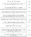
<도면의 주요 부분에 대한 부호의 설명><Explanation of symbols for main parts of the drawings>
10 : PCB11 : 접착제10: PCB 11: Adhesive
12 : 제1 칩13a, 13b : 전기접점12:
14 : 제2 칩15 : 제1 비아14
15a : 제1 비아홀15b : 제1 관통부15a: first via hole 15b: first through part
15c : 제1 랜드부16 : 제2 비아15c: first land portion 16: second via
16a : 제2 비아홀16b : 제2 관통부16a: second via hole 16b: second through part
16c : 제2 랜드부20 : 절연재16c: second land portion 20: insulating material
22 : 몰딩재30, 30a, 30b, 30c : 빌드업층22:
32 : 범프32: bump
본 발명은 전자 패키지 및 그 제조방법에 관한 것이다.The present invention relates to an electronic package and a method of manufacturing the same.
전자 패키지는 전자제품에서 사용되는 디바이스를 효율적으로 포장하는 기술로서, 낱개로 잘려진 반도체 칩을 기판(substrate)에 접착하고 전기적으로 연결하여 모듈화하는 칩 패키징(chip packaging) 기술을 포함하며, 초기의 삽입형 패키지 기술에서, 크기가 작고 전기적 성능이 우수한 표면실장용 패키지 기술을 거쳐, 최근에는 고밀도 실장기술, 주변 실장기술을 적용하여 BGA(Ball Grid Array), CSP(Chip Scale Package)와 같은 면실장 형태의 미소, 경량화 추세로 급속하게 발전하고 있다.Electronic packaging is a technology for efficiently packaging devices used in electronic products, and includes chip packaging technology that bonds and cuts semiconductor chips into substrates and electrically connects them. In package technology, through small size and excellent surface mount package technology, recently high density package technology and peripheral package technology are applied to surface mount type such as ball grid array (BGA) and chip scale package (CSP). It is rapidly developing into a smile and light weight trend.
현재의 CSP(Chip Scale Package)에는 플립칩(Flip chip) 공법이 적용되어, 칩 간 또는 칩과 기판 간의 전기적 연결을 위해 범프볼(Bump Ball) 기술이 필수적으로 사용되고 있다. 이러한 범프볼(Bump ball) 기술은 칩패드(chip pad)와의 연결부에서 열응력 등으로 인한 피로 균열(solder fatigue failure)이 발생하여 신뢰도에 문제가 있으며, 범프볼의 미세화의 한계로 인하여 패키지의 I/O 수가 제한된다 는 문제가 야기되는 실정이다.The current Chip Scale Package (CSP) is a flip chip method, and the bump ball technology is essentially used for electrical connection between chips or between a chip and a substrate. The bump ball technology has a problem of reliability due to the occurrence of solder fatigue failure due to thermal stress at the connection with the chip pad, and the I of the package due to the limitation of the miniaturization of the bump ball. The problem is that the number of / O is limited.
최근의 전자부품 산업에서는 칩(Chip)의 I/O수가 지속적으로 급격히 증가되고 있으며, 이에 따라 칩을 사용하여 제조되는 전자 패키지는 더욱 다기능화, 복합화되는 경향을 보이고 있다. 전술한 예와 관련하여, 플립칩(Flip Chip) BGA(Ball Grid Array) 패키지에서 솔더 범프(Solder Bump)를 사용하지 않고 칩의 전극 패드(Pad)를 칩 스케일(Chip Scale) 그대로 패키징(packaging)함으로써 I/O수의 제한을 받지 않고, 솔더 범프(Solder Bump)의 사용으로 인하여 발생할 수 있는 피로 균열(Solder fatigue)에 의한 제품의 신뢰도 저하의 문제를 해결할 수 있는 방법들이 개발되고 있다.In the recent electronic component industry, the number of chips (I / O) of chips is continuously increasing rapidly. Accordingly, electronic packages manufactured using chips tend to be more versatile and complex. In connection with the above-described example, the electrode pad of the chip is packaged as it is without the use of solder bumps in a flip chip Ball Grid Array (BGA) package. As a result, methods for solving the problem of deterioration of the reliability of the product due to fatigue fatigue, which may occur due to the use of solder bumps, are not being limited by the number of I / Os.
일례로서, 도 1 및 도 2 도시된 것과 같이 칩(chip) 상부의 전기접점 패턴(pattern)으로부터 금속(metal)층을 빌드업(build-up)해 나가는 이른바 '빌드업 기술'이 개발되었다. 그러나, 빌드업 기술의 경우에도 SIP(System In Package) 등의 패키지 구조를 형성하는 과정에서 패키지의 전체 사이즈가 커지게 된다는 문제를 안고 있다. 즉, 복수의 칩(multi Chip)을 사용하는 패키지의 경우에는 각각의 칩을 수평 정렬(horizontal array) 방식으로 실장해야 하므로 전체 세트(set)상의 패턴 사이즈를 최소화하기가 곤란하게 된다.As an example, a so-called 'build-up technology' has been developed for building up a metal layer from an electrical contact pattern on a chip as shown in FIGS. 1 and 2. However, even in the case of the build-up technology, the overall size of the package becomes large in the process of forming a package structure such as SIP (System In Package). That is, in the case of a package using a plurality of chips, it is difficult to minimize the pattern size on the entire set because each chip must be mounted in a horizontal array method.
또한, 솔더 범프를 사용하지 않는 종래의 플립칩 BGA 패키지의 경우, 고밀도의 I/O 패드(pad)를 가진 칩을 패키징할 수 있고, 범프볼(Bump Ball)을 사용하지 않으므로 그로 인한 피로 균열(Solder fatigue)의 문제가 발생하지 않는다는 잇점이 있는 반면, 패키지에 실장된 칩을 몰딩(Molding)하기 위한 별도의 공정이 반드 시 필요하고, 각 레이어(Layer)마다 접착층(Adhesive Layer)을 추가로 구성해야 하므로 공정이 매우 복잡하며, 몰딩재(Mold Material), 접착제(adhesive), 도전체 재료, PI(polyimide)와 같은 절연재 등 다양한 재료가 사용되므로 각 재료 간의 CTE(Coefficient of Thermal Expansion)의 차이 및 재료의 상이함으로 인하여 박리(delamination) 문제 등이 발생할 수 있고, 기존에 이미 소자가 실장되어 있는 PCB기판의 경우에는 적용될 수 없는 패키지 방법이라는 한계가 있다.In addition, conventional flip chip BGA packages that do not use solder bumps can package chips with high density I / O pads, and do not use bump balls, resulting in fatigue cracking ( While there is an advantage that solder fatigue does not occur, a separate process for molding chips mounted in a package is required, and an additional adhesive layer is formed for each layer. The process is very complicated, and various materials such as molding material, adhesive, conductor material, and insulating material such as polyimide (PI) are used, so the difference of the coefficient of thermal expansion (CTE) between each material and Due to the difference in materials, a delamination problem may occur, and there is a limitation in that a package method cannot be applied to a PCB substrate in which a device is already mounted.
본 발명은 소자가 실장되어 있는 PCB 상에 고밀도 반도체 칩을 실장하여 COC(chip on chip) 패키지를 구성하고 여기에 빌드업 기술을 적용한 전자 패키지 및 그 제조방법을 제공하는 것이다.SUMMARY OF THE INVENTION The present invention provides an electronic package and a method of manufacturing the same.
본 발명의 일 측면에 따르면, 일면에 제1 칩(chip)이 실장된 PCB(Printed Circuit Board)를 제공하는 단계, 일면에 전기접점이 형성된 제2 칩(chip)의 타면을 PCB의 타면에 어태칭(attaching)하는 단계, PCB의 타면에 절연재를 코팅하여 제2 칩을 인캡슐레이팅(encapsulating)하는 단계, 및 절연재를 천공하여 전기접점과 전기적으로 연결되는 제1 비아(via)를 가공하는 단계를 포함하는 전자 패키지 제조방법이 제공된다.According to an aspect of the invention, providing a printed circuit board (PCB) having a first chip (chip) mounted on one surface, the other surface of the second chip (chip) formed with an electrical contact on one surface to the other surface of the PCB Attaching, encapsulating the second chip by coating an insulating material on the other side of the PCB, and processing a first via electrically connected to the electrical contact by drilling the insulating material. An electronic package manufacturing method comprising a is provided.
가공단계 이후에, 절연재에 빌드업(build-up)층을 적층하고 빌드업층을 천공 하여 제1 비아와 전기적으로 연결되는 제2 비아를 가공하는 빌드업 단계를 더 포함할 수 있다. 빌드업층은 복수로 적층되고, 제2 비아는 복수의 빌드업층에 각각 가공될 수 있다.After the processing step, a build-up step of stacking a build-up layer on the insulating material and drilling the build-up layer may further include a build-up step of processing a second via electrically connected to the first via. The buildup layer may be stacked in plural, and the second via may be processed in the plurality of buildup layers, respectively.
빌드업 단계 이후에, 빌드업층의 표면에 제2 비아와 전기적으로 연결되는 도전성 범프(bump)를 형성하는 단계를 더 포함할 수 있다. 절연재와 빌드업층은 동일한 재질로 이루어지는 것이 바람직하다.After the buildup step, the method may further include forming a conductive bump electrically connected to the second via on the surface of the buildup layer. It is preferable that an insulation material and a buildup layer consist of the same material.
제공 단계는, PCB의 일면에 제1 칩을 실장하고 전기적으로 연결하는 단계, PCB의 일면에 몰딩재를 코팅하여 제1 칩을 몰딩(modling)하는 단계를 포함할 수 있고, 어태칭 단계는, 제2 칩과 PCB 사이에 접착제(adhesive)를 개재시켜 제2 칩을 PCB에 접착시키는 단계를 포함할 수 있으며, 인캡슐레이팅 단계는, 제2 칩을 커버하도록 PCB에 액상의 수지를 도포하고 소성(curing)시키는 단계를 포함할 수 있다.The providing step may include mounting and electrically connecting the first chip to one surface of the PCB, and coating the molding material on one surface of the PCB to mold the first chip, wherein the attaching step may include: Bonding the second chip to the PCB by interposing an adhesive between the second chip and the PCB, the encapsulating step includes applying a liquid resin to the PCB to cover the second chip and firing (curing) may be included.
가공단계는, 전기접점이 노출되도록 절연재를 드릴링(drilling)하여 비아홀(via hole)을 천공하는 단계, 및 비아홀의 표면을 도금(plating)하여 제1 비아를 형성하는 단계를 포함할 수 있다.The machining step may include drilling a via hole by drilling an insulating material to expose the electrical contact, and plating a surface of the via hole to form a first via.
또한, 본 발명의 다른 측면에 따르면, PCB(Printed Circuit Board)와, PCB의 일면에 실장되는 제1 칩(chip)과, PCB의 일면에 적층되며, 제1 칩을 인캡슐레이팅(encapsulating)하는 몰딩(molding)재와, 일면이 PCB의 타면에 접합되고, 타면에 전기접점이 형성된 제2 칩과, PCB의 타면에 적층되며, 제2 칩을 인캡슐레이팅하는 절연재와, 절연재의 표면에 형성되는 제1 랜드부와 절연재에 삽입되어 제1 랜드부와 전기접점을 전기적으로 연결하는 제1 관통부로 이루어지는 제1 비아(via)를 포 함하는 전자 패키지가 제공된다.In addition, according to another aspect of the present invention, a PCB (Printed Circuit Board), a first chip (chip) mounted on one side of the PCB, and laminated on one side of the PCB, encapsulating the first chip (encapsulating) A molding material, a second chip having one surface bonded to the other surface of the PCB and having electrical contacts formed on the other surface, an insulating material laminated on the other surface of the PCB and encapsulating the second chip, and formed on the surface of the insulating material. An electronic package including a first via formed of a first land portion and a first through portion inserted into an insulating material and electrically connecting the first land portion to an electrical contact is provided.
한편, 절연재에 적층되는 빌드업(build-up)층과, 빌드업층을 관통하여 제1 비아와 전기적으로 연결되는 제2 비아를 더 포함할 수 있다. 빌드업층은 복수로 적층되고, 제2 비아는 복수의 빌드업층에 각각 가공되어 서로 전기적으로 연결되도록 복수로 형성될 수 있다.On the other hand, it may further include a build-up layer laminated on the insulating material, and a second via electrically connected to the first via through the build-up layer. The buildup layer may be stacked in plural, and the second via may be formed in plural to be processed in the plurality of buildup layers and electrically connected to each other.
복수의 제2 비아는 서로 이격되어 복수의 빌드업층을 각각 관통하는 복수의 제2 관통부와, 복수의 빌드업층의 표면에 각각 형성되어 제2 관통부와 전기적으로 연결되는 복수의 제2 랜드부를 포함할 수 있다.The plurality of second vias are spaced apart from each other, and the plurality of second through portions penetrating the plurality of build up layers, respectively, and the plurality of second land portions formed on the surfaces of the plurality of build up layers, respectively, and electrically connected to the second through portions. It may include.
빌드업층의 표면에 형성되어 제2 비아와 전기적으로 연결되는 도전성 범프(bump)를 더 포함할 수 있다. 절연재와 빌드업층은 동일한 재질로 이루어질 수 있다.The semiconductor device may further include a conductive bump formed on the surface of the build-up layer and electrically connected to the second via. The insulating material and the buildup layer may be made of the same material.
제1 칩과 제2 칩은 제1 비아를 통해 서로 전기적으로 연결될 수 있다. 제1 관통부는, 전기접점이 노출되도록 절연재를 드릴링(drilling)하여 비아홀(via hole)을 형성하고, 비아홀의 표면을 도금(plating)함으로써 형성될 수 있다.The first chip and the second chip may be electrically connected to each other through the first via. The first through part may be formed by drilling an insulating material to expose an electrical contact to form a via hole, and plating a surface of the via hole.
전술한 것 외의 다른 측면, 특징, 잇점이 이하의 도면, 특허청구범위 및 발명의 상세한 설명으로부터 명확해질 것이다.Other aspects, features, and advantages other than those described above will become apparent from the following drawings, claims, and detailed description of the invention.
이하, 본 발명에 따른 전자 패키지 및 그 제조방법의 바람직한 실시예를 첨부도면을 참조하여 상세히 설명하기로 하며, 첨부 도면을 참조하여 설명함에 있어, 동일하거나 대응하는 구성 요소는 동일한 도면번호를 부여하고 이에 대한 중복되는 설명은 생략하기로 한다.Hereinafter, a preferred embodiment of an electronic package and a method of manufacturing the same according to the present invention will be described in detail with reference to the accompanying drawings, in the description with reference to the accompanying drawings, the same or corresponding components are given the same reference numerals and Duplicate description thereof will be omitted.
도 3은 본 발명의 바람직한 일 실시예에 따른 전자 패키지 제조방법을 나타낸 순서도이고, 도 4는 본 발명의 바람직한 일 실시예에 따른 전자 패키지 제조공정을 나타낸 흐름도이다. 도 4를 참조하면, PCB(10), 접착제(11), 제1 칩(12), 전기접점(13a, 13b), 제2 칩(14), 제1 비아(15), 제1 비아홀(15a), 제1 관통부(15b), 제1 랜드부(15c), 제2 비아(16), 제2 비아홀(16a), 제2 관통부(16b), 제2 랜드부(16c), 절연재(20), 몰딩재(22), 빌드업층(30, 30a, 30b, 30c), 범프(32)가 도시되어 있다.3 is a flowchart illustrating a method of manufacturing an electronic package according to an exemplary embodiment of the present invention, and FIG. 4 is a flowchart illustrating a process of manufacturing an electronic package according to an exemplary embodiment of the present invention. Referring to FIG. 4, the
본 실시예는 일면에 제1 칩(12)이 이미 실장되어 있는 PCB(10)의 타면에 고밀도 I/O를 갖는 제2 칩(14)을 접착한 후, 빌드업 기술을 적용하여 칩 간의 전기적 연결(interconnection) 및 제1 칩(12)과 제2 칩(14)에 대한 전기적 연결을 구현함으로써, 솔더 범프(Solder Bump)를 사용하지 않고도 보다 간단한 공정으로 높은 신뢰성을 확보할 수 있는 전자 패키지에 관한 것이다.In this embodiment, after bonding the
즉, 본 실시예에 따르면, 이미 제1 칩(12)이 실장되어 있는 PCB(10)의 타면에 고밀도 I/O를 가진 제2 칩(14)을 접착하여 패키징함으로써 제2 칩(14)의 실장과정을 보다 안정적으로 핸들링(handling)할 수 있으며, 제2 칩(14)에 대한 인캡슐레이션(Encapsulation) 재료와 빌드업층(30)의 재료를 후술하는 바와 같이 동일한 재료로 함으로써, 칩의 인캡슐레이션을 위해 별도의 공정을 도입할 필요가 없어 공정이 간단하다.That is, according to the present exemplary embodiment, the
즉, 본 실시예에 따라 전자 패키지를 제조하기 위해서는 먼저 일면에 제1 칩(12)이 실장된 PCB(10)를 제공하고(100), PCB(10)의 타면, 즉 제1 칩이 실장되지 않은 쪽의 면에 제2 칩(14)을 어태칭(attaching)한다(110). 어태칭 공정은 도 4의 (a)에 도시된 것처럼 접착제(11)를 개재시켜 칩을 PCB(10)에 접착시키는 공정으로 이루어진다. 이로써, 저렴하고 신속하게 칩을 PCB(10)에 어태칭할 수 있게 된다.That is, in order to manufacture the electronic package according to the present embodiment, first, the PCB 10 having the
제1 칩(12)이 실장된 PCB(10)는, PCB(10)의 일면에 제1 칩(12)을 실장하고 전기적으로 연결한 후(102), EMC(Epoxy molding compound) 등의 몰딩재(22)를 코팅하여 제1 칩(12)을 몰딩함으로써(104) 제공될 수 있다. 도 4에는 제1 칩(12)의 전기접점(13a)이 와이어 본딩(wire bonding)에 의해 PCB(10)에 전기적으로 연결된 상태가 도시되어 있으나, 제1 칩(12)의 전기적 연결 방법 및 몰딩 방법이 반드시 본 실시예에 한정되는 것은 아님은 물론이다.The
제2 칩(14)의 한쪽 면에는 전기접점(13b)이 형성되어 있으며, 후술하는 것과 같이 빌드업 기술을 적용하여 전기접점(13b)에 대한 전기적 연결을 구현하기 위해 도 4의 (b)와 같이 전기접점(13b)이 형성된 면이 노출되도록, 즉 전기접점(13b)이 형성되지 않은 면을 PCB(10)에 접합한다.An
이와 같이 제1 칩(12)이 실장된 PCB(10)의 타면에 제2 칩(14)을 실장함으로써 복수의 칩이 실장되는 전자 패키지가 제조된다. 제1 칩(12)과 제2 칩(14)은 PCB를 통해 전기적으로 연결될 수 있으며, 보다 구체적으로는 후술하는 빌드업 공정을 진행함에 따라 제2 칩(14)처럼 비아(15, 16)를 통해 직접 전기접점으로부터의 전기적 연결이 구현되거나, 제1 칩(12)처럼 PCB(10)를 통해 전기적 연결이 구현될 수 있다.As described above, the
제2 칩(14)이 어태칭된 상태에서 도 4의 (b)와 같이 PCB(10)에 절연재(20)를 코팅하여 적층된 칩을 절연재(20) 내에 수용시켜 커버하는 인캡슐레이팅(encapsulating) 공정을 진행한다(120).Encapsulating to accommodate and cover the stacked chips in the insulating
본 실시예에서는 PCB의 타면에 하나의 반도체 칩이 실장된 상태를 예로 들어 설명하였으나, 패키지의 설계에 따라서는 2개 이상의 칩을 적층(stack)하거나, 수평 정렬 방식으로 실장한 후 인캡슐레이팅하여 패키징할 수 있음은 물론이다.In this embodiment, a state in which one semiconductor chip is mounted on the other surface of the PCB has been described as an example. However, depending on the design of the package, two or more chips may be stacked or encapsulated after mounting in a horizontal alignment method. Of course it can be packaged.
인캡슐레이팅 공정은 도 4의 (b)와 같이 PCB(10) 상에 액상의 PI(polyimide) 레진(resin)을 도포하여 적층된 칩을 커버하고 이를 소성시키는 공정으로 진행될 수 있다. 후술하는 바와 같이 절연재에 비아홀을 천공하여 전기적 연결통로를 형성하는 빌드업 공정을 진행하기 위해서는 인캡슐레이트된 제2 칩(14) 상에 소정 두께의 절연층(Dielectric Layer)이 형성되어 있어야 하는데, 본 실시예에서와 같이 액상의 PI 레진을 도포한 후 경화시키는 경우에는 칩의 인캡슐레이션과 첫번째 절연층의 형성이 동시에 이루어지게 되어 공정이 간단해지는 효과가 있다.The encapsulation process may be performed by applying a liquid PI (polyimide) resin (resin) on the
절연재(20)가 경화된 후에는 빌드업 기술을 적용하여 제2 칩(14)의 전기접점(13b)의 위치에 상응하는 제1 비아(15)를 가공한다(130). 제1 비아(15)의 가공은 도 4의 (c)와 같이 전기접점(13b)이 노출되도록 레이저(laser) 드릴 등을 사용하여 절연재(20)를 천공하고(132), 도 4의 (d)와 같이 제1 비아홀(15a)의 표면에 Cu 스퍼터링(sputtering), 도전성 페이스트 충전 등의 공정을 적용하여 도금층이 형성되도록 한다(134). 제1 비아(15)를 통해 제1 칩(12)과의 전기적 연결도 구현되어야 하므로, 제1 비아홀(15a)은 제2 칩(14)의 전기접점(13b) 뿐만 아니라, 제1 칩(12) 이 전기적으로 연결된 PCB(10) 상의 접점(13c)이 노출되도록 천공되는 것이 좋다.After the insulating
이로써, 내장된 제2 칩(14)의 전기접점(13b)이 외부와 전기적으로 연결될 수 있게 된다. 비아홀의 천공에 사용되는 드릴링 공정 및 비아홀을 전기적으로 도통시키기 위한 도금 공정이 전술한 실시예에 한정되지 않음은 물론이다.As a result, the
도 4의 (d)에 도시된 것처럼 절연재(20)에 제1 비아홀(15a)을 천공하고 그 표면을 도금하여 제1 비아(15)를 형성할 경우, 제1 비아(15)는 절연재(20)를 관통하여 제2 칩(14)의 전기접점(13b)과 전기적 연결통로를 이루는 부분과, 그에 연결되어 절연재(20)의 표면에 일부 적층되는 부분으로 이루어지며, 이하 전자를 관통부, 후자를 랜드부로 명명하여 설명한다. 즉, 제1 비아(15)는 제1 비아홀(15a), 제1 관통부(15b), 제1 랜드부(15c)로 이루어진다.As shown in FIG. 4D, when the first via
다음으로, 필요에 따라 빌드업 공정을 계속 진행하여 반도체 칩과의 전기적 연결통로를 형성한다. 빌드업층(30)의 적층 횟수 및 비아홀의 가공은 전자 패키지의 설계에 따라 달라질 수 있다. 도 4는 총 3개의 빌드업층(30)을 적층하고 솔더볼 범프를 결합한 사례를 도시한 것이다.Next, if necessary, the build-up process is continued to form an electrical connection path with the semiconductor chip. The number of stacks of the build-
즉, 도 4의 (e)와 같이 절연재(20)에 첫번째 빌드업층(30a)을 적층한다. 빌드업층(30a)은 절연성 재질로 이루어지며, 절연재(20)와 동일한 재료인 액상 PI를 도포하여 경화시키거나, PI 필름을 적층하여 구현할 수 있다.That is, as shown in FIG. 4E, the
빌드업층(30)을 절연재(20)와 동일한 재료로 할 경우에는 칩의 인캡슐레이팅 공정과 빌드업층(30)의 적층 공정, 즉 빌드업 공정을 동일한 프로세스로 할 수 있어 가공성이 우수하고 비용이 저렴하며, 칩에서 발생하는 열로 인한 전자 패키지의 수축, 팽창이 절연재(20)와 빌드업층(30)에서 다르지 않기 때문에 열응력에 의한 에러를 방지할 수 있다. 따라서, 본 실시예에 따른 절연재(20) 및 빌드업층(30)의 재질의 동일함은 같은 재료뿐만 아니라 가공성, 비용, 열에 의한 수축, 팽창 정도 등에 있어서 같은 성질을 갖는 '동종의 재료'를 포함하는 개념이다.When the
다음으로 도 4의 (f)와 같이 제1 비아(15)의 위치에서 첫번째 빌드업층(30a)을 드릴링하여 제2 비아홀(16a)을 천공하고, 도 4의 (g)와 같이 제2 비아홀(16a)의 내면을 도금하여 제2 비아(16)를 형성한다(140). 제2 비아(16)도 제1 비아(15)와 마찬가지로 제2 비아홀(16a), 제2 랜드부(16c), 제2 관통부(16b)로 이루어지며, 도 4의 (g)에 도시된 것처럼 제1 랜드부(15c)가 노출되도록 제2 비아홀(16a)을 천공함으로써 제2 관통부(16b)가 제1 랜드부(15c)와 전기적으로 연결된다. 이로써, PCB(10) 및 반도체 칩(14)의 전기접점(13b, 13c)으로부터의 전기적 연결통로가 구현된다.Next, as shown in FIG. 4F, the first build-up
도 4는 3개의 빌드업층(30)을 적층하는 빌드업 공정의 예로서, 첫번째 빌드업 공정을 3회 반복한다. 즉, 도 4의 (h)와 같이 두번째 빌드업층(30b)을 적층하고, 도 4의 (i)와 같이 첫번째 빌드업층(30a)의 제2 비아(16)의 위치에서 제2 비아홀(16a)을 천공한 후, 도 4의 (j)와 같이 천공된 제2 비아홀(16a)을 도금하여 제2 비아(16)가 두번째 빌드업층(30b)까지 더 연결되도록 한다.4 is an example of a buildup process in which three
이러한 공정을 세번째 빌드업층(30c)의 경우에도 반복하여, 도 4의 (k)와 같이 세번째 빌드업층(30c)을 적층하고, 도 4의 (l)과 같이 두번째 빌드업층(30b)의 제2 비아(16)의 위치에서 제2 비아홀(16a)을 천공한 후, 도 4의 (m)과 같이 천공된 제2 비아홀(16a)을 도금하여 제2 비아(16)가 세번째 빌드업층(30c)까지 더 연결되도록 한다.This process is repeated for the
전술한 것과 같이 빌드업 공정은 전자 패키지의 설계에 따라 필요한 횟수만큼 복수로 진행되며, 이에 따라 빌드업층(30)이 복수로 적층되고 각 빌드업층(30)에 제2 비아(16)가 가공되어 전기적 연결통로를 구현한다. 제2 비아(16)의 전기적 연결은 제1 비아(15)와의 전기적 연결과 마찬가지로 n번째 빌드업층의 제2 랜드부(16c)와 (n+1)번째 빌드업층의 제2 관통부(16b)가 서로 연결되도록 함으로써 구현된다.As described above, the build-up process is performed a plurality of times as necessary according to the design of the electronic package. Accordingly, a plurality of build-up
빌드업 공정이 완료된 후에는 도 4의 (n)과 같이 빌드업층(30)의 표면에 형성된 제2 랜드부(16c)에 솔더볼(solder ball) 등의 도전성 범프를 결합하여 전자 패키지와 외부 장치와의 전기적 연결을 위한 접점을 형성한다(150).After the build-up process is completed, as shown in (n) of FIG. 4, a conductive bump such as a solder ball is coupled to the
도 5는 본 발명의 바람직한 일 실시예에 따른 전자 패키지를 나타낸 단면도이다. 도 5를 참조하면, PCB(10), 접착제(11), 제1 칩(12), 전기접점(13a, 13b), 제2 칩(14), 제1 비아(15), 제1 관통부(15b), 제1 랜드부(15c), 제2 비아(16), 제2 관통부(16b), 제2 랜드부(16c), 절연재(20), 몰딩재(22), 빌드업층(30), 범프(32)가 도시되어 있다.5 is a cross-sectional view illustrating an electronic package according to an exemplary embodiment of the present invention. Referring to FIG. 5, the
본 실시예에 따른 전자 패키지는 소자가 이미 실장되어 있는 PCB에 접착제(adhesive)를 사용하여 고밀도 I/O 칩을 접합하여 전기적 연결(Interconnection)을 구현한 구조로서, 내장된 칩으로부터의 전기적 연결통로(Electrical Path)는 칩 상부의 전기접점(Pad)으로부터 빌드업 기술을 적용하여 형성되며, 빌드업층의 최상 부에는 패키지의 SMT(surface mount technology) 실장을 위하여 범프가 결합된다.The electronic package according to the present embodiment is a structure in which an electrical connection is realized by bonding high density I / O chips using an adhesive to an PCB in which a device is already mounted. The electrical path is formed by applying a build-up technology from a pad on the chip, and bumps are coupled to the top of the build-up layer for mounting surface mount technology (SMT) of the package.
즉, PCB 또는 반도체 칩으로부터의 전기적 연결통로(electrical path)를 전기접점(13b, 13c)으로부터 빌드업 공정을 진행하여 구현되므로 보다 미세한 피치의 구현이 가능하다. 예를 들어, 종래의 범프볼 기술을 적용하여 100마이크로미터 정도의 피치를 구현한다고 할 때, 본 실시예에 따른 빌드업 기술을 적용하여 30마이크로미터 정도의 피치를 구현할 수 있어 미세 피치 구현 및 그로 인한 패키지의 소형화에 기여할 수 있다.In other words, the electrical path from the PCB or the semiconductor chip (electrical path) is implemented by the build-up process from the electrical contacts (13b, 13c) it is possible to implement a finer pitch. For example, when a pitch of about 100 micrometers is realized by applying a conventional bump ball technique, a pitch of about 30 micrometers may be realized by applying a build-up technique according to the present embodiment, thereby realizing fine pitch and This can contribute to the miniaturization of the package.
도 5에 도시된 것처럼, 본 실시예에 따른 전자 패키지는 한쪽 면에 이미 제1 칩이 실장, 몰딩되어 있는 PCB(10)의 다른 쪽 면에 제2 칩(14)을 접합하고 절연재로 인캡슐레이팅하여 제조되므로, 제2 칩의 패키징 과정에서 보다 안정적인 핸들링이 가능하다.As shown in FIG. 5, in the electronic package according to the present exemplary embodiment, the
전술한 바와 같이 PCB(10)의 일면에는 이미 제1 칩(12)이 실장되고 몰딩재(22)에 의해 몰딩되어 있어, PCB(10)의 타면에 제2 칩(14)을 어태칭하고 빌드업 공정을 진행할 때 패키지의 핸들링을 보다 안정적으로 할 수 있다.As described above, the
PCB(10)의 타면에 제2 칩(14)을 어태칭하는 공정은 접착제(11)를 사용함으로써 저렴하고 신속하게 진행할 수 있다. PCB(10)상에 접합되는 제2 칩(14)은 전기접점(13b)이 노출되도록 함으로써 빌드업 공정에 의한 전기적 연결통로 구현을 가능하게 한다.The process of attaching the
PCB(10)의 타면에 접합된 제2 칩(14)은 액상의 PI 레진(resin)을 도포하는 등 절연재(20)를 사용하여 인캡슐레이팅(encapsulating)한다. 반도체 칩의 몰딩은 EMC(Epoxy molding compound) 등 기존의 몰딩재로 인캡슐레이팅할 수도 있으며, 빌드업층(30)의 재질과 동일한 PI 레진 등을 사용하면 칩 인캡슐레이팅 공정과 빌드업 공정을 동일한 프로세스로 진행할 수 있어 공정이 단순하고, 재료 간의 물성차이로 인한 패키지의 에러를 방지할 수 있다.The
제2 칩(14)을 그 내부에 수용하여 인캡슐레이팅한 절연재(20)에는 제1 비아(15)가 관삽(貫揷)되어 PCB(10) 및 제2 칩(14)과의 전기적 연결통로를 구성한다. 제1 비아(15)는 절연재(20)의 표면에 형성되는 제1 랜드부(15c)와, 절연재(20)에 삽입되는 제1 관통부(15b)로 이루어지며, 도 4에서 설명한 바와 같이 제1 관통부(15b)는 전기접점(13b, 13c)이 노출되도록 절연재(20)를 드릴링하여 비아홀을 천공하고, 비아홀의 표면을 도금함으로써 형성된다. 이로써, 제1 비아(15)가 절연재(20)에 관삽된 형태로 칩과의 전기적 연결통로를 구현하게 된다. 또한, 이와 같이 형성된 제1 비아(15)를 통해 PCB(10)의 일면에 실장된 제1 칩(12)과 PCB(10)의 타면에 접합된 제2 칩(14)도 전기적으로 연결될 수 있다.The first via 15 is inserted into the insulating
본 실시예에 따른 빌드업 공법을 적용하게 되면, 절연재(20)에는 빌드업층(30)이 하나 또는 복수로 적층되며, 빌드업층(30)에는 제1 비아(15)와 전기적으로 연결되는 제2 비아(16)가 관삽된다. 제2 비아(16)는 각 빌드업층(30)에 형성되어 PCB(10) 및 제2 칩(14)의 전기접점(13b, 13c)으로부터의 전기적 연결통로를 형성하는 역할을 한다.When the build-up method according to the present embodiment is applied, one or more build-up
제2 비아(16) 또한 제1 비아(15)와 마찬가지로 빌드업층(30)에 관삽된 제2 관통부(16b)와 빌드업층(30)의 표면에 적층된 제2 랜드부(16c)로 이루어지며, 각 빌드업층(30)에 형성되는 복수의 제2 비아(16)는 도 5에 도시된 것처럼, 어느 한 층의 제2 관통부(16b)와 그에 인접한 층의 제2 랜드부(16c)가 서로 전기적으로 연결되는 구조로 형성된다. 이는 전기접점(13b, 13c)으로부터의 전기적 통로를 구현하기 위해 빌드업 공정을 적용함에 따라 형성되는 구조로서, 반드시 관통부와 랜드부가 접하는 형태로 이루어져야 하는 것은 아니며, 필요에 따라서는, 관통부끼리 연통되도록 하는 이른바 '스택 비아(stack via)' 구조 또는 적층된 전체 빌드업층(30)을 관통하는 쓰루홀(through hole) 구조로 전기적 통로가 구현될 수 있음은 물론이다.Like the first via 15, the second via 16 also includes a second through
빌드업 공정이 완료된 후에는 전자 패키지를 외부 장치에 SMT(surface mount technology) 실장 등을 통해 연결하기 위해 빌드업층(30)의 표면에 솔더볼 등의 도전성 범프를 결합한다. 도전성 범프는 빌드업층(30)에 형성된 제2 비아(16)와 전기적으로 연결되어 전자 패키지와 외부 장치 간의 전기적 연결을 위한 접점을 이루게 된다.After the buildup process is completed, a conductive bump such as solder balls is coupled to the surface of the
전술한 실시예 외의 많은 실시예들이 본 발명의 특허청구범위 내에 존재한다.Many embodiments other than the above-described embodiments are within the scope of the claims of the present invention.
상술한 바와 같이 본 발명의 바람직한 실시예에 따르면, 소자가 실장되어 있는 PCB 상에 고밀도 I/O의 반도체 칩을 더 적층(stack)하여 칩 간의 전기적 연 결(electrical interconnection)이 구현된 COC(chip on chip) 패키지를 구성하고, 솔더 범프 대신 빌드업 기술을 적용함으로써, 반도에 칩의 실장과정에서 안정적인 핸들링이 가능하고 칩의 인캡슐레이션(encapsulation)을 위한 별도의 공정이 불필요하며, 고밀도 및 신뢰성이 우수한 SIP(System in package)을 실현할 수 있다.As described above, according to the preferred embodiment of the present invention, a semiconductor chip of high density I / O is further stacked on a PCB on which the device is mounted, thereby implementing electrical interconnection between chips. on-chip package and build-up technology instead of solder bumps allow stable handling during chip mounting on the peninsula, eliminating the need for separate encapsulation, high density and reliability This excellent system in package (SIP) can be realized.
또한, 반도체 칩의 인캡슐레이션(encapsulation) 재료와 빌드업 재료를 동종의 재질로 함으로써, 칩의 인캡슐레이션을 위해 별도의 공정을 진행할 필요가 없어 공정이 단순화되고, 원가절감 및 수율향상에 기여하며, CTE 차이 및 재료의 상이함으로 인한 박리(delamination) 문제 등을 방지할 수 있다.In addition, by using the encapsulation material and the buildup material of the semiconductor chip as the same material, there is no need to perform a separate process for encapsulation of the chip, thereby simplifying the process and contributing to cost reduction and yield improvement. In addition, it is possible to prevent a delamination problem due to the difference in the CTE and the difference of the material.
Claims (17)
Translated fromKoreanPriority Applications (3)
| Application Number | Priority Date | Filing Date | Title |
|---|---|---|---|
| KR1020070020937AKR100851072B1 (en) | 2007-03-02 | 2007-03-02 | Electronic package and manufacturing method thereof |
| JP2008000731AJP4830120B2 (en) | 2007-03-02 | 2008-01-07 | Electronic package and manufacturing method thereof |
| US12/007,590US20080211083A1 (en) | 2007-03-02 | 2008-01-11 | Electronic package and manufacturing method thereof |
Applications Claiming Priority (1)
| Application Number | Priority Date | Filing Date | Title |
|---|---|---|---|
| KR1020070020937AKR100851072B1 (en) | 2007-03-02 | 2007-03-02 | Electronic package and manufacturing method thereof |
Publications (1)
| Publication Number | Publication Date |
|---|---|
| KR100851072B1true KR100851072B1 (en) | 2008-08-12 |
Family
ID=39732486
Family Applications (1)
| Application Number | Title | Priority Date | Filing Date |
|---|---|---|---|
| KR1020070020937AExpired - Fee RelatedKR100851072B1 (en) | 2007-03-02 | 2007-03-02 | Electronic package and manufacturing method thereof |
Country Status (3)
| Country | Link |
|---|---|
| US (1) | US20080211083A1 (en) |
| JP (1) | JP4830120B2 (en) |
| KR (1) | KR100851072B1 (en) |
Cited By (4)
| Publication number | Priority date | Publication date | Assignee | Title |
|---|---|---|---|---|
| KR101109214B1 (en) | 2009-12-28 | 2012-01-30 | 삼성전기주식회사 | Package board and its manufacturing method |
| KR101174554B1 (en) | 2009-03-12 | 2012-08-16 | 애플 인크. | Flexible packaging for chip-on-chip and package-on-package technologies |
| KR20130083932A (en)* | 2010-12-22 | 2013-07-23 | 인텔 코포레이션 | Substrate with embedded stacked through-silicon via die |
| US11462466B2 (en) | 2019-10-22 | 2022-10-04 | Samsung Electronics Co., Ltd. | Fan-out type semiconductor packages and methods of manufacturing the same |
Families Citing this family (13)
| Publication number | Priority date | Publication date | Assignee | Title |
|---|---|---|---|---|
| JP5147755B2 (en)* | 2009-02-20 | 2013-02-20 | 新光電気工業株式会社 | Semiconductor device and manufacturing method thereof |
| JP5280945B2 (en)* | 2009-06-19 | 2013-09-04 | 新光電気工業株式会社 | Semiconductor device and manufacturing method thereof |
| US20110108999A1 (en)* | 2009-11-06 | 2011-05-12 | Nalla Ravi K | Microelectronic package and method of manufacturing same |
| KR20130007371A (en)* | 2011-07-01 | 2013-01-18 | 삼성전자주식회사 | Semiconductor package |
| WO2013095444A1 (en) | 2011-12-21 | 2013-06-27 | Intel Corporation | Packaged semiconductor die and cte-engineering die pair |
| KR101947722B1 (en)* | 2012-06-07 | 2019-04-25 | 삼성전자주식회사 | stack semiconductor package and method of manufacturing the same |
| TWI596715B (en)* | 2014-09-12 | 2017-08-21 | 矽品精密工業股份有限公司 | Semiconductor package and manufacturing method thereof |
| KR20170085833A (en)* | 2016-01-15 | 2017-07-25 | 삼성전기주식회사 | Electronic component package and manufactruing method of the same |
| US10297575B2 (en) | 2016-05-06 | 2019-05-21 | Amkor Technology, Inc. | Semiconductor device utilizing an adhesive to attach an upper package to a lower die |
| TWI624016B (en)* | 2017-08-16 | 2018-05-11 | 矽品精密工業股份有限公司 | Electronic package and the manufacture thereof |
| JP7046639B2 (en)* | 2018-02-21 | 2022-04-04 | 新光電気工業株式会社 | Wiring board and its manufacturing method |
| KR102800191B1 (en) | 2020-07-28 | 2025-04-28 | 삼성전자주식회사 | Semiconductor package |
| US11638359B2 (en) | 2021-05-05 | 2023-04-25 | Toyota Motor Engineering & Manufacturing North America, Inc. | Low profile power module package |
Citations (1)
| Publication number | Priority date | Publication date | Assignee | Title |
|---|---|---|---|---|
| KR20050073678A (en)* | 2004-01-09 | 2005-07-18 | 주식회사 하이닉스반도체 | Method for manufacturing bga type package |
Family Cites Families (8)
| Publication number | Priority date | Publication date | Assignee | Title |
|---|---|---|---|---|
| US5111278A (en)* | 1991-03-27 | 1992-05-05 | Eichelberger Charles W | Three-dimensional multichip module systems |
| JP3366062B2 (en)* | 1992-07-02 | 2003-01-14 | モトローラ・インコーポレイテッド | Overmold type semiconductor device and method of manufacturing the same |
| US5438216A (en)* | 1992-08-31 | 1995-08-01 | Motorola, Inc. | Light erasable multichip module |
| US6271469B1 (en)* | 1999-11-12 | 2001-08-07 | Intel Corporation | Direct build-up layer on an encapsulated die package |
| US6680529B2 (en)* | 2002-02-15 | 2004-01-20 | Advanced Semiconductor Engineering, Inc. | Semiconductor build-up package |
| JP4027788B2 (en)* | 2002-12-10 | 2007-12-26 | 新光電気工業株式会社 | Manufacturing method of electronic component mounting structure |
| JP4438389B2 (en)* | 2003-11-14 | 2010-03-24 | カシオ計算機株式会社 | Manufacturing method of semiconductor device |
| JP4413798B2 (en)* | 2005-02-25 | 2010-02-10 | 日本シイエムケイ株式会社 | Manufacturing method of semiconductor device |
- 2007
- 2007-03-02KRKR1020070020937Apatent/KR100851072B1/ennot_activeExpired - Fee Related
- 2008
- 2008-01-07JPJP2008000731Apatent/JP4830120B2/ennot_activeExpired - Fee Related
- 2008-01-11USUS12/007,590patent/US20080211083A1/ennot_activeAbandoned
Patent Citations (1)
| Publication number | Priority date | Publication date | Assignee | Title |
|---|---|---|---|---|
| KR20050073678A (en)* | 2004-01-09 | 2005-07-18 | 주식회사 하이닉스반도체 | Method for manufacturing bga type package |
Cited By (7)
| Publication number | Priority date | Publication date | Assignee | Title |
|---|---|---|---|---|
| KR101174554B1 (en) | 2009-03-12 | 2012-08-16 | 애플 인크. | Flexible packaging for chip-on-chip and package-on-package technologies |
| KR101109214B1 (en) | 2009-12-28 | 2012-01-30 | 삼성전기주식회사 | Package board and its manufacturing method |
| KR20130083932A (en)* | 2010-12-22 | 2013-07-23 | 인텔 코포레이션 | Substrate with embedded stacked through-silicon via die |
| KR101581699B1 (en)* | 2010-12-22 | 2015-12-31 | 인텔 코포레이션 | Substrate with embedded stacked through-silicon via die |
| US10461032B2 (en) | 2010-12-22 | 2019-10-29 | Intel Corporation | Substrate with embedded stacked through-silicon via die |
| US11107766B2 (en) | 2010-12-22 | 2021-08-31 | Intel Corporation | Substrate with embedded stacked through-silicon via die |
| US11462466B2 (en) | 2019-10-22 | 2022-10-04 | Samsung Electronics Co., Ltd. | Fan-out type semiconductor packages and methods of manufacturing the same |
Also Published As
| Publication number | Publication date |
|---|---|
| US20080211083A1 (en) | 2008-09-04 |
| JP4830120B2 (en) | 2011-12-07 |
| JP2008218979A (en) | 2008-09-18 |
Similar Documents
| Publication | Publication Date | Title |
|---|---|---|
| KR100851072B1 (en) | Electronic package and manufacturing method thereof | |
| US12334445B2 (en) | Method of fabricating a semiconductor package | |
| US10212818B2 (en) | Methods and apparatus for a substrate core layer | |
| US6784530B2 (en) | Circuit component built-in module with embedded semiconductor chip and method of manufacturing | |
| KR101134123B1 (en) | Semiconductor device | |
| US7514770B2 (en) | Stack structure of carrier board embedded with semiconductor components and method for fabricating the same | |
| US7586183B2 (en) | Multilevel semiconductor module and method for fabricating the same | |
| US9847236B2 (en) | Electrical interconnect structure for an embedded electronics package | |
| US7839649B2 (en) | Circuit board structure having embedded semiconductor element and fabrication method thereof | |
| US20180240789A1 (en) | Stackable electronic package and method of fabricating same | |
| JP3277997B2 (en) | Ball grid array package and manufacturing method thereof | |
| US8058723B2 (en) | Package structure in which coreless substrate has direct electrical connections to semiconductor chip and manufacturing method thereof | |
| KR20160032985A (en) | Package board, method for manufacturing the same and package on package having the thereof | |
| KR20150135046A (en) | Package board, method for manufacturing the same and package on packaage having the thereof | |
| KR100838352B1 (en) | Carrying structure of electronic components | |
| CN111009500A (en) | Semiconductor package, method of manufacturing the same, and method of manufacturing redistribution structure | |
| US20160104652A1 (en) | Package structure and method of fabricating the same | |
| KR100872125B1 (en) | Semiconductor package and manufacturing method | |
| KR100836642B1 (en) | Electronic package and manufacturing method thereof | |
| CN115224006A (en) | Semiconductor package and method of manufacturing the same | |
| CN108305864B (en) | Terminal with a terminal body | |
| KR100836657B1 (en) | Electronic package and manufacturing method thereof | |
| KR100836645B1 (en) | Electronic package and manufacturing method thereof | |
| US20240096721A1 (en) | Electronic package and manufacturing method thereof | |
| KR100855624B1 (en) | Semiconductor package and manufacturing method |
Legal Events
| Date | Code | Title | Description |
|---|---|---|---|
| A201 | Request for examination | ||
| PA0109 | Patent application | St.27 status event code:A-0-1-A10-A12-nap-PA0109 | |
| PA0201 | Request for examination | St.27 status event code:A-1-2-D10-D11-exm-PA0201 | |
| R18-X000 | Changes to party contact information recorded | St.27 status event code:A-3-3-R10-R18-oth-X000 | |
| D13-X000 | Search requested | St.27 status event code:A-1-2-D10-D13-srh-X000 | |
| D14-X000 | Search report completed | St.27 status event code:A-1-2-D10-D14-srh-X000 | |
| E902 | Notification of reason for refusal | ||
| PE0902 | Notice of grounds for rejection | St.27 status event code:A-1-2-D10-D21-exm-PE0902 | |
| E13-X000 | Pre-grant limitation requested | St.27 status event code:A-2-3-E10-E13-lim-X000 | |
| P11-X000 | Amendment of application requested | St.27 status event code:A-2-2-P10-P11-nap-X000 | |
| P13-X000 | Application amended | St.27 status event code:A-2-2-P10-P13-nap-X000 | |
| E701 | Decision to grant or registration of patent right | ||
| PE0701 | Decision of registration | St.27 status event code:A-1-2-D10-D22-exm-PE0701 | |
| GRNT | Written decision to grant | ||
| PR0701 | Registration of establishment | St.27 status event code:A-2-4-F10-F11-exm-PR0701 | |
| PR1002 | Payment of registration fee | St.27 status event code:A-2-2-U10-U11-oth-PR1002 Fee payment year number:1 | |
| PG1601 | Publication of registration | St.27 status event code:A-4-4-Q10-Q13-nap-PG1601 | |
| PR1001 | Payment of annual fee | St.27 status event code:A-4-4-U10-U11-oth-PR1001 Fee payment year number:4 | |
| PR1001 | Payment of annual fee | St.27 status event code:A-4-4-U10-U11-oth-PR1001 Fee payment year number:5 | |
| FPAY | Annual fee payment | Payment date:20130624 Year of fee payment:6 | |
| PR1001 | Payment of annual fee | St.27 status event code:A-4-4-U10-U11-oth-PR1001 Fee payment year number:6 | |
| R18-X000 | Changes to party contact information recorded | St.27 status event code:A-5-5-R10-R18-oth-X000 | |
| FPAY | Annual fee payment | Payment date:20140701 Year of fee payment:7 | |
| PR1001 | Payment of annual fee | St.27 status event code:A-4-4-U10-U11-oth-PR1001 Fee payment year number:7 | |
| FPAY | Annual fee payment | Payment date:20150707 Year of fee payment:8 | |
| PR1001 | Payment of annual fee | St.27 status event code:A-4-4-U10-U11-oth-PR1001 Fee payment year number:8 | |
| LAPS | Lapse due to unpaid annual fee | ||
| PC1903 | Unpaid annual fee | St.27 status event code:A-4-4-U10-U13-oth-PC1903 Not in force date:20160802 Payment event data comment text:Termination Category : DEFAULT_OF_REGISTRATION_FEE | |
| PC1903 | Unpaid annual fee | St.27 status event code:N-4-6-H10-H13-oth-PC1903 Ip right cessation event data comment text:Termination Category : DEFAULT_OF_REGISTRATION_FEE Not in force date:20160802 | |
| R18-X000 | Changes to party contact information recorded | St.27 status event code:A-5-5-R10-R18-oth-X000 |