KR100850950B1 - Nitride based light emitting diode - Google Patents
Nitride based light emitting diodeDownload PDFInfo
- Publication number
- KR100850950B1 KR100850950B1KR1020060070214AKR20060070214AKR100850950B1KR 100850950 B1KR100850950 B1KR 100850950B1KR 1020060070214 AKR1020060070214 AKR 1020060070214AKR 20060070214 AKR20060070214 AKR 20060070214AKR 100850950 B1KR100850950 B1KR 100850950B1
- Authority
- KR
- South Korea
- Prior art keywords
- layer
- type semiconductor
- light emitting
- emitting device
- nitride
- Prior art date
- Legal status (The legal status is an assumption and is not a legal conclusion. Google has not performed a legal analysis and makes no representation as to the accuracy of the status listed.)
- Active
Links
Images


Classifications
- H—ELECTRICITY
- H10—SEMICONDUCTOR DEVICES; ELECTRIC SOLID-STATE DEVICES NOT OTHERWISE PROVIDED FOR
- H10H—INORGANIC LIGHT-EMITTING SEMICONDUCTOR DEVICES HAVING POTENTIAL BARRIERS
- H10H20/00—Individual inorganic light-emitting semiconductor devices having potential barriers, e.g. light-emitting diodes [LED]
- H10H20/80—Constructional details
- H10H20/81—Bodies
- H10H20/811—Bodies having quantum effect structures or superlattices, e.g. tunnel junctions
- H10H20/812—Bodies having quantum effect structures or superlattices, e.g. tunnel junctions within the light-emitting regions, e.g. having quantum confinement structures
- B—PERFORMING OPERATIONS; TRANSPORTING
- B82—NANOTECHNOLOGY
- B82Y—SPECIFIC USES OR APPLICATIONS OF NANOSTRUCTURES; MEASUREMENT OR ANALYSIS OF NANOSTRUCTURES; MANUFACTURE OR TREATMENT OF NANOSTRUCTURES
- B82Y20/00—Nanooptics, e.g. quantum optics or photonic crystals
- H—ELECTRICITY
- H10—SEMICONDUCTOR DEVICES; ELECTRIC SOLID-STATE DEVICES NOT OTHERWISE PROVIDED FOR
- H10H—INORGANIC LIGHT-EMITTING SEMICONDUCTOR DEVICES HAVING POTENTIAL BARRIERS
- H10H20/00—Individual inorganic light-emitting semiconductor devices having potential barriers, e.g. light-emitting diodes [LED]
- H10H20/80—Constructional details
- H10H20/81—Bodies
- H10H20/822—Materials of the light-emitting regions
- H10H20/824—Materials of the light-emitting regions comprising only Group III-V materials, e.g. GaP
- H10H20/825—Materials of the light-emitting regions comprising only Group III-V materials, e.g. GaP containing nitrogen, e.g. GaN
Landscapes
- Chemical & Material Sciences (AREA)
- Engineering & Computer Science (AREA)
- Nanotechnology (AREA)
- Physics & Mathematics (AREA)
- Life Sciences & Earth Sciences (AREA)
- Biophysics (AREA)
- Optics & Photonics (AREA)
- Crystallography & Structural Chemistry (AREA)
- Led Devices (AREA)
- Semiconductor Lasers (AREA)
Abstract
Translated fromKoreanDescription
Translated fromKorean도 1은 일반적인 발광 소자의 일례를 나타내는 단면도이다.1 is a cross-sectional view showing an example of a general light emitting device.
도 2는 도 1의 밴드 다이어그램이다.FIG. 2 is a band diagram of FIG. 1.
도 3은 본 발명의 제1실시예를 나타내는 단면도이다.3 is a cross-sectional view showing a first embodiment of the present invention.
도 4는 도 3의 밴드 다이어그램이다.4 is a band diagram of FIG. 3.
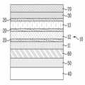
도 5는 본 발명의 제2실시예를 나타내는 단면도이다.5 is a cross-sectional view showing a second embodiment of the present invention.
도 6은 본 발명의 제3실시예를 나타내는 단면도이다.6 is a cross-sectional view showing a third embodiment of the present invention.
도 7은 도 6의 밴드 다이어그램이다.7 is a band diagram of FIG. 6.
도 8은 본 발명의 제3실시예의 제3층과 제4층의 제1예를 나타내는 밴드 다이어그램이다.Fig. 8 is a band diagram showing a first example of the third layer and the fourth layer of the third embodiment of the present invention.
도 9는 본 발명의 제3실시예의 제3층과 제4층의 제2예를 나타내는 밴드 다이어그램이다.Fig. 9 is a band diagram showing a second example of the third layer and the fourth layer in the third embodiment of the present invention.
도 10은 본 발명의 제3실시예의 제3층과 제4층의 제3예를 나타내는 밴드 다이어그램이다.Fig. 10 is a band diagram showing a third example of the third layer and the fourth layer of the third embodiment of the present invention.
도 11은 본 발명의 제3실시예의 제3층과 제4층의 제4예를 나타내는 밴드 다이어그램이다.Fig. 11 is a band diagram showing a fourth example of the third layer and the fourth layer of the third embodiment of the present invention.
도 12는 본 발명의 제3실시예의 제3층과 제4층의 제5예를 나타내는 밴드 다 이어그램이다.12 is a band diagram showing a fifth example of the third layer and the fourth layer of the third embodiment of the present invention.
<도면의 주요 부분에 대한 간단한 설명><Brief description of the main parts of the drawing>
10 : 제1층 20 : 제2층10: first layer 20: second layer
30 : 활성층 40 : 기판30: active layer 40: substrate
50 : 버퍼층 60 : n-형 반도체층50: buffer layer 60: n-type semiconductor layer
70 : p-형 반도체층 80 : 제3층70: p-type semiconductor layer 80: third layer
90 : 제4층90: the fourth layer
본 발명은 질화물계 발광 소자에 관한 것으로 특히, 발광 소자의 발광 효율과 신뢰성을 향상시킬 수 있는 질화물계 발광 소자에 관한 것이다.The present invention relates to a nitride-based light emitting device, and more particularly to a nitride-based light emitting device that can improve the luminous efficiency and reliability of the light emitting device.
발광 다이오드(Light Emitting Diode: LED)는 전류를 빛으로 변환시키는 잘 알려진 반도체 발광 소자로서, 1962년 GaAsP 화합물 반도체를 이용한 적색 LED가 상품화 된 것을 시작으로 GaP:N 계열의 녹색 LED와 함께 정보 통신기기를 비롯한 전자장치의 표시 화상용 광원으로 이용되어 왔다.Light Emitting Diodes (LEDs) are well-known semiconductor light emitting devices that convert current into light.In 1962, red LEDs using GaAsP compound semiconductors were commercialized, along with GaP: N series green LEDs. It has been used as a light source for display images of electronic devices, including.
이러한 LED에 의해 방출되는 광의 파장은 LED를 제조하는데 사용되는 반도체 재료에 따른다. 이는 방출된 광의 파장이 가전자대(valence band) 전자들과 전도대(conduction band) 전자들 사이의 에너지 차를 나타내는 반도체 재료의 밴드갭(band-gap)에 따르기 때문이다.The wavelength of light emitted by such LEDs depends on the semiconductor material used to make the LEDs. This is because the wavelength of the emitted light depends on the band-gap of the semiconductor material, which represents the energy difference between the valence band electrons and the conduction band electrons.
질화 갈륨 화합물 반도체(Gallium Nitride: GaN)는 높은 열적 안정성과 폭넓은 밴드갭(0.8 ~ 6.2eV)을 가지고 있어, LED를 포함한 고출력 전자부품 소자 개발 분야에서 많은 주목을 받아왔다.Gallium nitride compound semiconductors (Gallium Nitride (GaN)) have high thermal stability and wide bandgap (0.8 to 6.2 eV), which has attracted much attention in the development of high-power electronic components including LEDs.
이에 대한 이유 중 하나는 GaN이 타 원소들(인듐(In), 알루미늄(Al) 등)과 조합되어 녹색, 청색 및 백색광을 방출하는 반도체 층들을 제조할 수 있기 때문이다.One reason for this is that GaN can be combined with other elements (indium (In), aluminum (Al), etc.) to produce semiconductor layers that emit green, blue and white light.
이와 같이 방출 파장을 조절할 수 있기 때문에 특정 장치 특성에 맞추어 재료의 특징들에 맞출 수 있다. 예를 들어, GaN를 이용하여 광기록에 유익한 청색 LED와 백열등을 대치할 수 있는 백색 LED를 만들 수 있다.In this way, the emission wavelength can be adjusted to match the material's characteristics to specific device characteristics. For example, GaN can be used to create white LEDs that can replace incandescent and blue LEDs that are beneficial for optical recording.
이러한 GaN 계열 물질의 이점들로 인해, GaN 계열의 LED 시장이 급속히 성장하고 있다. 따라서, 1994년에 상업적으로 도입한 이래로 GaN 계열의 광전자장치 기술도 급격히 발달하였다.Due to the advantages of these GaN-based materials, the GaN-based LED market is growing rapidly. Therefore, since commercial introduction in 1994, GaN-based optoelectronic device technology has rapidly developed.
상술한 바와 같은 GaN 계열 물질을 이용한 LED의 휘도 또는 출력은 크게, 활성층의 구조, 빛을 외부로 추출할 수 있는 광추출 효율, LED 칩의 크기, 램프 패키지 조립 시 몰드(mold)의 종류 및 각도, 형광물질 등에 의해서 좌우된다.The brightness or output of the LED using the GaN-based material as described above is large, the structure of the active layer, the light extraction efficiency to extract light to the outside, the size of the LED chip, the type and angle of the mold (mold) when assembling the lamp package , Fluorescent material and the like.
한편, 이러한 GaN 계열 반도체 성장이 다른 Ⅲ-Ⅴ족 화합물 반도체보다 어려운 이유 중에 하나는 고품질의 기판, 즉, GaN, InN, AlN 등의 물질의 웨이퍼가 존재하지 않기 때문이다.On the other hand, one of the reasons why the growth of GaN-based semiconductors is more difficult than other III-V compound semiconductors is that there are no high-quality substrates, that is, wafers made of materials such as GaN, InN, and AlN.
따라서 사파이어와 같은 이종 기판 위에 LED 구조를 성장하게 되며, 이때 많은 결함이 발생하게 되고, 이러한 결함들은 LED 성능에 큰 영향을 미치게 된다.Therefore, the LED structure is grown on a heterogeneous substrate such as sapphire, and many defects are generated, and these defects have a great influence on the LED performance.
이러한 GaN 계열 물질의 LED의 기본 구조는 도 1에서 도시하는 바와 같이, n-형 반도체층(1)이 위치하고, 이러한 n-형 반도체층(1)과 인접하여 양자우물구조를 가지는 활성층(2)이 위치하며, 이 활성층(2)과 인접하여 p-형 반도체층(3)이 위치한다. 도 2는 이와 같은 LED 구조의 에너지 밴드 구조를 나타내고 있다.As shown in FIG. 1, the basic structure of the LED of the GaN-based material includes an n-
이러한 LED 구조는 기판(4) 위에 성장된 상태를 나타내며, 이러한 LED 구조는 기판(4)상의 버퍼층(5) 위에 형성된다.This LED structure represents a state grown on the
이후에 이러한 LED 구조에는 전극(도시되지 않음)이 형성되어, 이러한 전극을 통한 전하의 주입에 의하여 발광이 가능하게 된다.Thereafter, an electrode (not shown) is formed in the LED structure, thereby enabling light emission by injection of charge through the electrode.
상기 활성층(2) 중에서 특히 우물층은 InGaN, AlGaN 등의 물질로 형성되며, 이러한 활성층(2)은 하측에 위치하는 n-형 반도체층(1)을 이루는 GaN 물질과는 큰 격자상수의 차이를 보인다.In particular, the well layer of the
따라서 얇은 두께를 이루는 활성층(2)의 우물층은 그 하측에 위치하는 두꺼운 n-형 반도체층(1)에 의하여 큰 스트레인(strain)을 받게 된다.Therefore, the well layer of the
즉, 활성층(2)을 이루는 InGaN의 격자상수는 그 하측에 위치하는 GaN보다 커서 InGaN 성장시 압축 응력(compressive strain)을 받으며 성장된다.That is, the lattice constant of InGaN constituting the
이러한 활성층(2)에 작용하는 스트레인은 박막 품질을 저하시키고 LED의 발광 효율을 감소시킬 수 있어, 이러한 스트레인을 감소시키기 위한 효과적인 대안이 요구된다.Strain acting on this
본 발명이 이루고자 하는 기술적 과제는, 발광 소자의 스트레인 및 결정 결 함을 조절 또는 억제하고, 전자와 정공이 활성층으로 효율적으로 구속되도록 함으로써 신뢰성 특성을 향상시킬 수 있는 질화물계 발광 소자를 제공하는 데 있다.An object of the present invention is to provide a nitride-based light emitting device that can improve the reliability characteristics by controlling or suppressing the strain and crystal defects of the light emitting device, and to effectively confine the electrons and holes in the active layer. .
상기 기술적 과제를 이루기 위한 제1관점으로서, 본 발명은, 발광 소자에 있어서, n-형 반도체층과; p-형 반도체층과; 상기 n-형 반도체층과 p-형 반도체층 사이에 위치하며, 적어도 한쌍 이상의 우물층과 장벽층으로 이루어지는 활성층과; 상기 n-형 반도체층과 활성층 사이 및 상기 p-형 반도체층과 활성층 사이의 경계면 중 적어도 어느 하나의 경계면에 위치하며, 밴드갭 또는 두께가 변동하는 복수의 층으로 이루어지는 제1층과; 상기 복수의 제1층 사이에 위치하는 제2층을 포함하여 구성되는 것이 바람직하다.As a first aspect for achieving the above technical problem, the present invention provides a light emitting device comprising: an n-type semiconductor layer; a p-type semiconductor layer; An active layer disposed between the n-type semiconductor layer and the p-type semiconductor layer, the active layer comprising at least one pair of well layers and a barrier layer; A first layer disposed on at least one interface between the n-type semiconductor layer and the active layer and between the p-type semiconductor layer and the active layer, the first layer comprising a plurality of layers having varying band gaps or thicknesses; It is preferable to comprise the 2nd layer located between the said 1st layer.
상기 제1층은, 밴드갭이 상기 활성층에 가까와질수록 감소하도록 형성될 수 있고, 이러한 제1층의 밴드갭은, 상기 n-형 반도체층 또는 p-형 반도체층과 상기 우물층 사이의 값을 가지는 것이 바람직하다.The first layer may be formed such that a band gap decreases closer to the active layer, and the band gap of the first layer is a value between the n-type semiconductor layer or the p-type semiconductor layer and the well layer. It is preferable to have.
또한, 상기 제1층은, InGaN 또는 AlInGaN 물질로 이루어질 수 있으며, 상기 제1층이 InGaN로 이루어지는 경우, InxGa1-xN의 In 조성 x는, 0.1과 0.15 사이(0.1 ≤ x ≤ 0.15)인 것이 바람직하다.Further, the first layer may be made of InGaN or AlInGaN material, and when the first layer is made of InGaN, the In composition x of Inx Ga1-x N may be between 0.1 and 0.15 (0.1 ≦ x ≦ 0.15 Is preferable.
상기 활성층은 GaN, InGaN, AlInGaN 물질 중 적어도 어느 하나 이상으로 이루어질 수 있고, 상기 제2층은, GaN 물질로 이루어질 수 있다.The active layer may be made of at least one of GaN, InGaN, and AlInGaN materials, and the second layer may be made of GaN material.
상기 제1층 및 제2층은, 상기 활성층과, 상기 n-형 반도체층 및 p-형 반도체 층 중에서 상기 활성층 이전에 성장되는 층 사이에 위치하는 것이 바람직하다.The first layer and the second layer are preferably located between the active layer and a layer grown before the active layer among the n-type semiconductor layer and the p-type semiconductor layer.
상기 제1층의 두께는 50 내지 1000Å이고, 상기 제2층의 두께는 5 내지 500Å인 것이 바람직하다.It is preferable that the thickness of a said 1st layer is 50-1000 GPa, and the thickness of a said 2nd layer is 5-500 GPa.
한편, 상기 제1층은, 두께가 상기 활성층에 가까와질수록 두꺼워지도록 형성될 수 있으며, 이때, 상기 제1층의 밴드갭은 일정하게 유지되는 것이 바람직하다.Meanwhile, the first layer may be formed to become thicker as the thickness approaches the active layer, and in this case, the band gap of the first layer is preferably kept constant.
상기 제1층 및 제2층은, 3개 이상 구성될 수 있다.The first layer and the second layer may be composed of three or more.
상기 기술적 과제를 이루기 위한 제2관점으로서, 본 발명은, 발광 소자에 있어서, 제1전극과 연결되는 n-형 반도체층과; 제2전극과 연결되는 p-형 반도체층과; 상기 n-형 반도체층과 p-형 반도체층 사이에 위치하는 활성층과; 상기 n-형 반도체층과 p-형 반도체층 및 활성층과의 경계면 중 적어도 하나의 경계면에 위치하며, 상기 n-형 반도체층 또는 p-형 반도체층보다 큰 밴드갭을 가지는 복수의 제3층과; 상기 복수의 제3층 사이에 위치하는 제4층을 포함하여 구성되는 것이 바람직하다.As a second aspect of the present invention, there is provided a light emitting device comprising: an n-type semiconductor layer connected to a first electrode; A p-type semiconductor layer connected to the second electrode; An active layer positioned between the n-type semiconductor layer and the p-type semiconductor layer; A plurality of third layers positioned at at least one interface between the n-type semiconductor layer, the p-type semiconductor layer, and the active layer and having a larger bandgap than the n-type semiconductor layer or the p-type semiconductor layer; ; It is preferable to comprise the 4th layer located between the said 3rd layer.
상기 제3층은, AlGaN 또는 AlInGaN 물질로 이루어질 수 있으며, 상기 AlGaN 물질의 조성은, AlxInyGa1-x-yN로 표현되는 경우에 x는 0.2 이상(x ≥ 0.2)인 것이 바람직하다.The third layer may be made of AlGaN or AlInGaN material, the composition of the AlGaN material, when expressed as Alx Iny Ga1-xy N is preferably x is 0.2 or more (x ≥ 0.2).
또한, 상기 제4층은, GaN, AlGaN, InGaN, AlInGaN, 및 AlInN 중 어느 하나의 물질로 이루어질 수 있으며, 상기 제4층이 AlInGaN 물질로 이루어지는 경우, AlxInyGa1-x-yN로 표현되는 경우에 x는 0.2 이하(x ≤ 0.2)인 것이 바람직하다.In addition, the fourth layer may be made of any one of GaN, AlGaN, InGaN, AlInGaN, and AlInN, and when the fourth layer is made of AlInGaN, it is represented by Alx Iny Ga1-xy N. In this case, x is preferably 0.2 or less (x ≦ 0.2).
한편, 상기 제3층은, 경사진 에너지 밴드 구조를 가질 수 있다.Meanwhile, the third layer may have an inclined energy band structure.
이러한 경사진 에너지 밴드 구조는, 톱니 형상, 삼각형, 사다리꼴 형상, 및 M자형 중 어느 하나인 것이 바람직하다.This inclined energy band structure is preferably any one of a sawtooth shape, a triangle, a trapezoidal shape, and an M shape.
이하, 첨부된 도면을 참고하여 본 발명에 의한 실시예를 상세히 설명하면 다음과 같다.Hereinafter, exemplary embodiments of the present invention will be described in detail with reference to the accompanying drawings.
<제1실시예>First Embodiment
도 3은 본 발명의 제1실시예로서 서로 다른 In 조성을 갖는 InGaN으로 이루어지는 제1층(10)들과 이들 각각의 제1층(10)을 이루는 각각의 층(11, 12, 13) 사이에 위치하는 GaN으로 이루어지는 제2층(20)이 활성층(30) 하측에 삽입한 구조를 도시하고 있다.FIG. 3 shows a first embodiment between the
이러한 구조는 기판(40) 위에 버퍼층(50)이 형성되고, 이러한 버퍼층(50) 위에 n-형 반도체층(60)이 위치하며, 이 n-형 반도체층(60) 위에는 상기 제1층(10)과 제2층(20)이 번갈아 형성된다.In this structure, the
이와 같은 제1층(10)과 제2층(20) 위에는 활성층(30)이 위치하고, 이 활성층(30) 위에는 p-형 반도체층(70)이 형성된다.The
이때, 상기 제1층(10)은 상기 n-형 반도체층(60)으로부터 첫번째 InGaN 층(11)의 In 조성을 기준으로 두번째 InGaN 층(12)은 첫번째 In 조성보다 많은 In 조성을 가지며, 세번째 InGaN 층(13)의 In 조성은 두번째 InGaN 층(12)의 In 조성보다 많은 양을 가진다.In this case, the
따라서, 이들 InGaN으로 이루어지는 제1층(10)의 In 조성은 활성층(30)으로 가까와질수록 활성층(30)의 In 조성에 근접한 In 조성을 갖게 되며, 이러한 In 조 성은 활성층(30)의 In 조성보다는 작을 수 있다.Therefore, the In composition of the
이때, 이러한 제1층(10)의 In 조성이 점점 많아짐에 따라, 도 4에서와 같이, 밴드갭 에너지는 점차 활성층(30)에 가까와지며 점점 낮아진다.At this time, as the In composition of the
이러한 구조를 통하여 활성층(30)의 InGaN 물질의 성장시 n-형 반도체층(60) 위에 직접 성장될 때보다 더 작은 스트레인 또는 스트레스를 받게되어, 활성층(30)에서 고품질의 InGaN 우물층을 성장할 수 있다.Through this structure, the growth of the InGaN material in the
이와 함께, 도 4에서 도시하는 바와 같이, 제1층(10)의 밴드갭은 점차 활성층(30)에 가깝게 되므로, 활성층(30) 아래에 삽입된 제1층(10)의 3 개의 InGaN 층(11, 12, 13)들에 전하(carrier)가 포획되어 효율적으로 활성층(30)의 InGaN 우물층으로 주입(injection) 될 수 있다.4, the band gap of the
또한, 이들 InGaN 층(11, 12, 13)의 사이에 위치하는 제2층(20)은 이러한 InGaN 층(11, 12, 13)보다 얇게 형성될 수 있다.In addition, the
이와 같이, 얇은 두께의 제2층(20)은 전하의 흐름에 방해를 주지 않도록 할 수 있다.As such, the thin
이와 같이, 활성층(30)과 제1층(10)이 InGaN으로 이루어지는 경우, 이러한 제1층(10)에서 In의 조성은, InxGa1-xN에서 x는, 0.1과 0.15 사이(0.1 ≤ x ≤ 0.15)인 것이 바람직하다.As described above, in the case where the
한편, 활성층(30)이 InGaN으로 이루어진 경우, Al과 In의 조성을 조절하여 제1층(10)을 AlInGaN으로 형성할 수도 있다.Meanwhile, when the
또한, 이러한 제1층(10)의 두께는 50 내지 1000Å이고, 상기 제2층(20)의 두께는 5 내지 500Å인 것이 바람직하다.In addition, the thickness of the
본 실시예에서는 제1층(10)과 제2층(20)이 n-형 반도체층(60)과 활성층(30) 사이에 위치하는 경우를 설명하고 있으나, 이러한 제1층(10)과 제2층(20)은 성장 단계에서 활성층(30)의 하측에 위치하는 경우에 모두 적용될 수 있다.In the present exemplary embodiment, the case in which the
따라서, 만일 활성층(30)의 하측에 p-형 반도체층(70)이 위치한다면, 상기 제1층(10)과 제2층(20)은 이러한 활성층(30)과 p-형 반도체층(70) 사이에 위치할 수도 있다.Therefore, if the p-
또한, 본 실시예에서는 상기 활성층(30)이 InGaN으로 이루어진 경우를 예로 설명하였으나, GaN, AlGaN, AlInGaN 등으로 이루어진 경우에도 적용될 수 있음은 물론이다.In addition, in the present embodiment, the case in which the
상기 제2층(20)도 또한 GaN 이외에 InGaN, AlGaN, AlInGaN 등의 물질로 형성이 가능하다.The
또한, 본 실시예에서는 상기 제1층(10)을 이루는 각 층과 제2층(20)이 각각 3 개의 층(제1층의 각층과 제2층이 3개의 쌍)으로 이루어지는 실시예를 설명하고 있으나, 2 개(2개의 쌍) 이상의 층으로 이루어지면 본 발명의 효과를 발휘할 수 있다.In addition, in the present embodiment, an embodiment in which each layer and the
<제2실시예>Second Embodiment
도 5는 본 발명의 제2실시예로서 동일한 In 조성을 가지며 두께가 서로 다른 3 개의 InGaN으로 이루어지는 제1층(10)들과 이들 제1층(10)을 이루는 각각의 층(11, 12, 13)들 사이에 위치하는 GaN으로 이루어지는 제2층(20)이 활성층(30) 하측에 삽입한 구조를 나타내고 있다.FIG. 5 shows
이러한 구조는 기판(40) 위에 버퍼층(50)이 형성되고, 이러한 버퍼층(50) 위에 n-형 반도체층(60)이 위치하며, 이 n-형 반도체층(60) 위에는 상기 제1층(10)과 제2층(20)이 형성된다.In this structure, the
이와 같은 제1층(10)과 제2층(20) 위에는 활성층(30)이 위치하고, 이 활성층(30) 위에는 p-형 반도체층(70)이 형성된다.The
이때, 상기 제1층(10)은 상기 n-형 반도체층(60)으로부터 첫번째 InGaN 층(11)보다는 두번째 InGaN 층(12)이 두껍게 형성되고, 이 두번째 InGaN층(12)보다는 세번째 InGaN 층(13)이 두껍게 형성된다.In this case, the
또한, 이들 제1층(10)을 이루는 각각의 층(11, 12, 13)의 In 조성은 동일하며, 따라서 동일한 밴드갭 에너지를 가지게 된다.In addition, the In composition of each of the
따라서, 활성층(30)의 InGaN 성장시 n-형 반도체층(60) 위에 직접 성장할 때보다 더 작은 스트레인 또는 스트레스를 받게되어, 활성층(30)에서 고품질의 InGaN 우물층을 성장할 수 있다.Accordingly, when InGaN is grown in the
이와 함께 활성층(30) 아래에 삽입된 3 개의 InGaN 층(11, 12, 13) 들에 의하여 전하(carrier)가 포획되어 효율적으로 활성층(30)의 InGaN 우물층으로 주입(injection)될 수 있다.In addition, a carrier may be trapped by three InGaN layers 11, 12, and 13 inserted below the
이러한 서로 다른 두께를 가지는 층(11, 12, 13)으로 이루어지는 제1층(10)을 가지는 구조로부터, 제1층(10)을 이루는 InGaN 층의 두께가 두꺼워질수록 GaN에 의한 활성층의 압축 응력(compressive strain)이 약해지는 경향이 있으므로, 활성층(30)의 품질이 향상될 수 있다.From the structure having the
또한, 이들 InGaN 층(11, 12, 13)의 사이에 위치하는 제2층(20)은 이러한 InGaN 층(11, 12, 13)보다 얇게 형성되어, 이와 같이, 얇은 두께의 제2층(20)은 전하의 흐름에 방해를 주지 않도록 할 수 있다.In addition, the
이와 같이, 활성층(30)과 제1층(10)이 InGaN으로 이루어지는 경우, 이러한 제1층(10)에서 In의 조성은, InxGa1-xN에서 x는, 0.1과 0.15 사이(0.1 ≤ x ≤ 0.15)인 것이 바람직하다.As described above, in the case where the
한편, 활성층(30)이 InGaN으로 이루어진 경우, Al과 In의 조성을 조절하여 제1층(10)을 AlInGaN으로 형성할 수도 있다.Meanwhile, when the
또한, 이러한 제1층(10)의 두께는 50 내지 1000Å으로서, 제1층(10)을 이루는 각각의 층(11, 12, 13)은 상기 두께 범위에서 변경될 수 있고, 상기 제2층(20)의 두께는 5 내지 500Å인 것이 바람직하다.In addition, the thickness of the
본 실시예에서는 제1층(10)과 제2층(20)이 n-형 반도체층(60)과 활성층(30) 사이에 위치하는 경우를 설명하고 있으나, 상기 제1실시예에서 설명한 바와 같이, 이러한 제1층(10)과 제2층(20)은 성장 단계에서 활성층(30)의 하측에 위치하는 경우에 모두 적용될 수 있다.In the present embodiment, the case in which the
즉, 만일 활성층(30)의 하측에 p-형 반도체층(70)이 위치한다면, 상기 제1층(10)과 제2층(20)은 이러한 활성층(30)과 p-형 반도체층(70) 사이에 위치할 수도 있다.That is, if the p-
또한, 본 실시예에서는 상기 활성층(30)이 InGaN으로 이루어진 경우를 예로 설명하였으나, GaN, AlGaN, AlInGaN 등으로 이루어진 경우에도 적용될 수 있음은 물론이다.In addition, in the present embodiment, the case in which the
상기 제2층(20)도 또한 GaN 이외에 InGaN, AlGaN, AlInGaN 등의 물질로 형성이 가능하고, 상기 제1층(10)을 이루는 각 층과 제2층(20)이 2 개(2개의 쌍) 이상의 층으로 이루어지면 본 발명의 효과를 발휘할 수 있다.The
<제3실시예>Third Embodiment
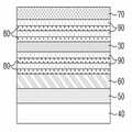
도 6에서는 본 발명의 제3실시예로서, 활성층(30)과 n-형 반도체층(60) 사이와, 활성층(30)과 p-형 반도체층(70) 사이에 제3층(80)과 제4층(90)이 교대로 삽입되어 위치한 구조를 도시하고 있다.In FIG. 6, as the third embodiment of the present invention, the
이러한 구조는 기판(40) 위에 버퍼층(50)이 형성되고, 이러한 버퍼층(50) 위에 n-형 반도체층(60)이 위치하며, 이 n-형 반도체층(60) 위에는 상기 제3층(80)과 제4층(90)이 형성된다.In this structure, the
이와 같은 제3층(80)과 제4층(90) 위에는 활성층(30)이 위치하고, 이 활성층(30) 위에는 다시 제3층(80)과 제4층(90)이 형성되고, 그 위에 p-형 반도체층(70)이 형성된다.The
본 실시예에서는 상기 제3층(80)과 제4층(90)이 활성층(30)과 n-형 반도체층(60) 사이와, 활성층(30)과 p-형 반도체층(70) 사이 모두에 위치한 상태를 설명하고 있으나, 둘 중 어느 한 곳에만 구성될 수도 있다.In the present embodiment, the
즉, 상기 제3층(80)과 제4층(90)이 활성층(30)과 n-형 반도체층(60) 사이에만 위치하거나, 활성층(30)과 p-형 반도체층(70) 사이에만 위치할 수도 있다.That is, the
상기 제3층(80)은 상기 n-형 반도체층(60) 또는 p-형 반도체층(70)을 이루는 GaN 보다 밴드갭이 큰 물질을 이용할 수 있으며, AlGaN, AlInGaN 등의 물질을 이용할 수 있다.As the
또한, 상기 제4층(90)은 GaN을 이용하는 것이 바람직하나, In과 Al의 성분이 적절히 조절된다면 InGaN, AlGaN, AlInGaN 등이 모두 이용될 수 있다.In addition, although the
즉, 상기 제3층은, AlGaN 또는 AlInGaN 물질로 이루어질 수 있으며, 상기 AlGaN 물질의 조성은, AlxInyGa1-x-yN로 표현되는 경우에 x는 0.2 이상(x ≥ 0.2)으로 이루어질 수 있다.That is, the third layer may be made of AlGaN or AlInGaN material, and the composition of the AlGaN material may be made of 0.2 or more (x ≥ 0.2) when expressed as Alx Iny Ga1-xy N. have.
또한, 상기 제4층은, GaN, AlGaN, InGaN, AlInGaN, 및 AlInN 중 어느 하나의 물질로 이루어질 수 있으며, 상기 제4층이 AlInGaN 물질로 이루어지는 경우, AlxInyGa1-x-yN로 표현되는 경우에 x는 0.2 이하(x ≤ 0.2)로 이루어질 수 있다.In addition, the fourth layer may be made of any one of GaN, AlGaN, InGaN, AlInGaN, and AlInN, and when the fourth layer is made of AlInGaN, it is represented by Alx Iny Ga1-xy N. X may be made 0.2 or less (x ≦ 0.2).
도 6에서는 제3층(80)과 제4층(90)이 두 개씩(2 쌍) 구성된 상태를 도시하고 있으나, 그 이상의 제3층(80)과 제4층(90)을 쌍으로 구성할 수 있다.In FIG. 6, the
도 7에서는 도 6과 같은 구조의 밴드 다이어그램을 도시하고 있다.FIG. 7 illustrates a band diagram of the structure shown in FIG. 6.
또한, 상기 AlGaN을 제3층(80)으로, 그리고 GaN을 제4층(90)으로 얇은 두께로 순차적으로 성장시킴으로써 응력을 받는 초격자층(strained layer superlattice: SLS)을 이용할 수도 있다.In addition, a stressed layer superlattice (SLS) may be used by sequentially growing the AlGaN into the
이러한 제3층(80)과 제4층(90)은 Mg와 같은 도펀트 물질로 도핑(doping)되어, 전도성 반도체층으로 형성될 수 있고, 특히, p-형 반도체 특성을 가질 수 있다.The
이때, 이러한 도핑은 제3층(80)과 제4층(90) 전체에 대하여 이루어질 수도 있고, 제3층(80)과 제4층(90) 각각을 델타 도핑(delta-doping) 함으로써 전도성을 띠게 할 수도 있다.In this case, the doping may be performed on the entirety of the
즉, 각각의 제3층(80)과 제4층(90)을 성장시에 도펀트 물질을 일차례씩 주입함으로써, 거의 단일층이 전도성을 가지도록 형성할 수 있다. 그러나 제3층(80)과 제4층(90) 전체를 도핑하는 것에 비하여 전도성은 저하되지 않는다.That is, by injecting the dopant material one time at a time during the growth of each of the third and
이러한 델타 도핑은 제3층(80)과 제4층(90)의 전도성은 저하시키지 않으면서, 도펀트 주입에 의한 박막 품질의 저하를 최소화할 수 있다.The delta doping may minimize the deterioration of thin film quality due to dopant implantation without reducing the conductivity of the
또한, 이러한 델타 도핑은 제3층(80)과 제4층(90) 각각의 중간부분, 활성층에 가까운 부분, 또는 활성층에서 먼 부분에 도펀트를 주입하여 전도성 반도체로 성장시킬 수 있다.In addition, the delta doping may be grown into a conductive semiconductor by injecting dopants in the middle portion of each of the
상기 활성층(30)의 양자우물구조를 이루는 우물층과 장벽층에 사용되는 GaN과 InGaN, AlGaN 등의 물질은 격자 상수가 크게 다르므로, 이와 같은 격자 상수의 차이에 의하여 큰 스트레인(strain)이 발생하게 되는데, 이러한 스트레인은 전위(dislocation)와 같은 결정 결함의 요소로 작용하게 된다.Since the lattice constants of GaN, InGaN, AlGaN, and the like used in the well layer and the barrier layer forming the quantum well structure of the
더욱이, 국부적으로 발생되는 스트레인은 광을 발생하기 위한 전자와 정공의 효율적 결합을 저해시키기 때문에 이러한 스트레인의 조절이 필요하다.Moreover, locally generated strains inhibit the efficient coupling of electrons and holes to generate light, and thus control of these strains is necessary.
종래의 GaN 계열 물질을 이용한 발광 소자의 개발에 있어서 고출력, 고효율의 발광 소자를 제작하기 위하여, n-형 반도체 층에서 형성된 전자가 활성층을 지나 p-형 반도체층까지 넘어오는 것을 방지하기 위한 electron blocking layer(EBL)로 p-형의 AlGaN 층을 이용한다.In the development of a light emitting device using a GaN-based material, electron blocking to prevent electrons formed in an n-type semiconductor layer from passing through an active layer to a p-type semiconductor layer in order to manufacture a light emitting device having high output and high efficiency. As a layer (EBL), a p-type AlGaN layer is used.
그러나, 이러한 p-형의 AlGaN을 단일층으로 이용할 경우 AlGaN의 p-형 특성이 좋지 않기 때문에 EBL 역할은 수행할 수 있으나 정공(hole)이 활성층으로 주입되는 것을 오히려 방해할 수 있다.However, when the p-type AlGaN is used as a single layer, since the p-type characteristic of AlGaN is not good, it may play an EBL role but may hinder the injection of holes into the active layer.
따라서, 이러한 p-형 AlGaN 층을 이용하지 않고, 제3층(80)과 제4층(90)을 반복하여 적층함으로써, 스트레인의 문제를 해결하면서 EBL층으로 이용될 수 있다.Accordingly, by repeatedly stacking the
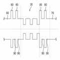
한편, 상기 제3층(80)은 형성시에 소스 성분의 양을 선형적으로 변화시켜(composition grading), 에너지 밴드 구조에 경사를 이루도록 구성할 수 있다.On the other hand, the
도 8 내지 도 12는 이와 같이 composition grading을 준 제3층(80)이 제4층과 SLS를 이루는 경우의 에너지 밴드의 형상을 나타내고 있다.8 to 12 show the shape of the energy band when the
도 8 및 도 9는 에너지 밴드가 큰 물질(AlGaN의 경우 Al)의 성분을 선형적으로 변화시켜 밴드 구조에서 제3층(80)이 톱니 형상의 경사(grading)를 이룬 경우에 해당한다.8 and 9 correspond to a case where the
이러한 구조는, 에너지 밴드가 큰 물질이 Al과 In이 포함된 ternary (AlGaN 계열) 또는 quarternary(AlInGaN 계열)로 구성되어 있으면, 반응할 수 있는 Al 소스(source)의 양을 점차 감소시켜 Al의 성분(composition)을 감소시킨다.This structure, if the material with a large energy band is composed of ternary (AlGaN series) or quarternary (AlInGaN series) containing Al and In, the amount of Al source that can react gradually decreases decrease composition
또는 In 소스의 양을 점차 증가시키거나 성장 온도를 감소시키면서 성장함으 로써 In 성분을 증가시켜 도 8과 같은 밴드 구조를 갖는 composition grading SLS를 성장시킬 수 있다.Alternatively, the composition grading SLS having a band structure as shown in FIG. 8 may be grown by increasing the In component by increasing the amount of the In source or increasing the growth temperature while decreasing the growth temperature.
도 9의 에너지 밴드 구조를 갖는 SLS의 성장은 도 8의 경우와 반대로 성장시킬 수 있다.The growth of the SLS having the energy band structure of FIG. 9 may be grown in the opposite manner to that of FIG. 8.
또한, Al, In의 양과 온도를 함께 변화시키는 경우에도 도 8 및 도 9의 에너지 밴드 구조를 갖는 SLS를 성장시킬 수 있다.In addition, even when the amounts of Al and In and the temperature are changed together, the SLS having the energy band structure of FIGS. 8 and 9 can be grown.
이러한 SLS의 성장은 활성층(30)의 양측에 다른 형태의 밴드 구조를 갖도록 형성할 수 있다. 예를 들면, 활성층(30)의 일측에는 도 8의 밴드 구조를 갖도록 하고, 활성층(30)의 타측에는 도 9의 밴드 구조를 갖도록 형성할 수 있다.The growth of the SLS may be formed to have a band structure of another type on both sides of the
보다 구체적인 예로서, 활성층(30)과 n-형 반도체층(60) 사이의 부분에는 도 9의 밴드 구조를 갖는 SLS 구조를 삽입하고, 활성층(30)과 p-형 반도체층(70) 사이에는 도 8의 밴드 구조를 갖는 SLS 구조를 삽입할 수 있다.As a more specific example, an SLS structure having the band structure of FIG. 9 is inserted into the portion between the
이와 같이, 대칭적인 구조를 갖는 SLS 구조를 삽입하면, 활성층(30)과 n-형 반도체층(60) 사이에서는 전자가 주입되는 경우에 상기 제3층(80)과 제4층(90)이 저항으로서 작용하지 않도록 하고, 활성층(30)과 p-형 반도체층(60) 사이에서는 EBL(electron blocking layer)층으로 작용할 수 있도록 함으로써, 활성층(30)에 전하가 용이하게 구속될 수 있도록 할 수 있는 것이다.As such, when the SLS structure having the symmetrical structure is inserted, when the electrons are injected between the
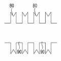
도 10 및 도 11은 각각 제3층(80)이 사다리꼴 및 삼각형의 밴드 구조를 이루도록 성장시킨 구조를 나타낸다.10 and 11 show a structure in which the
이러한 밴드 구조의 성장법은, 상기 도 8 및 도 9의 성장 방법을 동일하게 이용할 수 있다.The growth method of such a band structure can use the growth method of the said FIG. 8 and FIG. 9 similarly.
즉, 우선 도 9의 형상의 밴드 구조를 갖는 층을 성장시킨 후 에너지 밴드가 가장 큰 성분의 상태를 일정 시간 동안 유지시키고, 이후 도 8과 같은 구조를 갖는 층을 성장시키면 도 10과 같이 에너지 밴드가 큰 물질이 등변사다리꼴 또는 부등변 사다리꼴 형상의 에너지 밴드 구조를 갖는 SLS가 성장되게 된다.That is, first, the layer having the band structure of FIG. 9 is grown, and then the state of the component having the largest energy band is maintained for a predetermined time, and then the layer having the structure as shown in FIG. 8 is grown. The larger material will grow an SLS having an energy band structure having an isosceles trapezoid or an isosceles trapezoid shape.
또한, 도 11의 경우는 도 10의 구조를 성장시키는 방법에서 에너지 밴드가 가장 큰 성분 상태를 일정 시간 동안 유지하는 과정을 제외시키면 된다.In the case of FIG. 11, the process of growing the structure of FIG. 10 may exclude the process of maintaining the state of the component having the largest energy band for a predetermined time.
이와 같은 과정에서 에너지 밴드가 큰 물질이 양쪽으로 composition grading을 갖는 삼각형 형상을 갖는 SLS를 성장시킬 수 있다.In this process, a material having a large energy band may grow an SLS having a triangular shape having composition grading on both sides.
한편, 도 12의 경우는 도 10의 경우와 순서를 반대로 하여, 도 9의 밴드 구조를 갖는 층을 성장시킨 후 바로 도 9의 형상의 에너지 밴드를 갖는 물질을 성장시키면 된다.Meanwhile, in the case of FIG. 12, the material having the energy band having the shape of FIG. 9 may be grown immediately after the layer having the band structure of FIG. 9 is grown in the reverse order to that of FIG. 10.
이와 같은 도 12의 밴드 구조의 전도대(conduction band)는 영문 대문자 M자와 같은 구조를 이루게 된다.The conduction band of the band structure of FIG. 12 forms a structure like the capital letter M in English.
상기 실시예는 본 발명의 기술적 사상을 구체적으로 설명하기 위한 일례로서, 본 발명은 상기 실시예에 한정되지 않으며, 다양한 형태의 변형이 가능하고, 이러한 기술적 사상의 여러 실시 형태는 모두 본 발명의 보호범위에 속함은 당연하다.The above embodiment is an example for explaining the technical idea of the present invention in detail, and the present invention is not limited to the above embodiment, various modifications are possible, and various embodiments of the technical idea are all protected by the present invention. It belongs to the scope.
이상과 같은 본 발명은 다음과 같은 효과가 있는 것이다.The present invention as described above has the following effects.
첫째, 발광 소자의 스트레인을 완화시킴으로써 고품질의 박막을 형성할 수 있고, 따라서 발광 소자의 신뢰성이 향상된다.First, a high quality thin film can be formed by alleviating the strain of the light emitting device, thus improving the reliability of the light emitting device.
둘째, 활성층과의 경계면에서 캐리어의 흐름을 원활히 함으로서, 구동 전압을 낮추고 발광 효율을 향상시킬 수 있다.Second, by smoothing the flow of the carrier at the interface with the active layer, it is possible to lower the driving voltage and improve the luminous efficiency.
셋째, 활성층에 캐리어가 효율적으로 구속되도록 함으로써, 발광 소자의 발광 효율을 향상시킬 수 있다.Third, by efficiently constraining the carrier to the active layer, the light emission efficiency of the light emitting device can be improved.
Claims (19)
Translated fromKoreanPriority Applications (5)
| Application Number | Priority Date | Filing Date | Title |
|---|---|---|---|
| KR1020060070214AKR100850950B1 (en) | 2006-07-26 | 2006-07-26 | Nitride based light emitting diode |
| EP07113151AEP1883122A3 (en) | 2006-07-26 | 2007-07-25 | Nitride-based semiconductor light emitting device |
| US11/878,641US8350250B2 (en) | 2006-07-26 | 2007-07-25 | Nitride-based light emitting device |
| JP2007194942AJP5305277B2 (en) | 2006-07-26 | 2007-07-26 | Nitride-based light emitting device |
| TW096127300ATWI436495B (en) | 2006-07-26 | 2007-07-26 | Nitride-based illuminating device |
Applications Claiming Priority (1)
| Application Number | Priority Date | Filing Date | Title |
|---|---|---|---|
| KR1020060070214AKR100850950B1 (en) | 2006-07-26 | 2006-07-26 | Nitride based light emitting diode |
Publications (2)
| Publication Number | Publication Date |
|---|---|
| KR20080010136A KR20080010136A (en) | 2008-01-30 |
| KR100850950B1true KR100850950B1 (en) | 2008-08-08 |
Family
ID=38616306
Family Applications (1)
| Application Number | Title | Priority Date | Filing Date |
|---|---|---|---|
| KR1020060070214AActiveKR100850950B1 (en) | 2006-07-26 | 2006-07-26 | Nitride based light emitting diode |
Country Status (5)
| Country | Link |
|---|---|
| US (1) | US8350250B2 (en) |
| EP (1) | EP1883122A3 (en) |
| JP (1) | JP5305277B2 (en) |
| KR (1) | KR100850950B1 (en) |
| TW (1) | TWI436495B (en) |
Cited By (2)
| Publication number | Priority date | Publication date | Assignee | Title |
|---|---|---|---|---|
| US8426844B2 (en) | 2010-08-04 | 2013-04-23 | Lg Innotek Co., Ltd. | Light emitting device, light emitting device package, and display device therewith |
| KR101439652B1 (en) | 2012-11-27 | 2014-09-17 | 한국광기술원 | Light Emitting Diode of having Superlattice Layer |
Families Citing this family (49)
| Publication number | Priority date | Publication date | Assignee | Title |
|---|---|---|---|---|
| KR100703096B1 (en)* | 2005-10-17 | 2007-04-06 | 삼성전기주식회사 | Nitride semiconductor light emitting device |
| US7769066B2 (en)* | 2006-11-15 | 2010-08-03 | Cree, Inc. | Laser diode and method for fabricating same |
| US7834367B2 (en) | 2007-01-19 | 2010-11-16 | Cree, Inc. | Low voltage diode with reduced parasitic resistance and method for fabricating |
| US8519437B2 (en)* | 2007-09-14 | 2013-08-27 | Cree, Inc. | Polarization doping in nitride based diodes |
| US9012937B2 (en)* | 2007-10-10 | 2015-04-21 | Cree, Inc. | Multiple conversion material light emitting diode package and method of fabricating same |
| KR101018088B1 (en) | 2008-11-07 | 2011-02-25 | 삼성엘이디 주식회사 | Nitride semiconductor devices |
| KR20110062128A (en)* | 2009-12-02 | 2011-06-10 | 엘지이노텍 주식회사 | Light emitting device, light emitting device package and manufacturing method |
| JP4960465B2 (en) | 2010-02-16 | 2012-06-27 | 株式会社東芝 | Semiconductor light emitting device |
| KR101007136B1 (en)* | 2010-02-18 | 2011-01-10 | 엘지이노텍 주식회사 | Light emitting device, light emitting device package and manufacturing method |
| KR101766719B1 (en)* | 2010-03-25 | 2017-08-09 | 엘지이노텍 주식회사 | Light emitting diode and Light emitting device comprising the same |
| EP2408028B1 (en) | 2010-07-16 | 2015-04-08 | LG Innotek Co., Ltd. | Light emitting device |
| KR101134408B1 (en)* | 2010-08-04 | 2012-04-09 | 엘지이노텍 주식회사 | Light emitting device |
| KR101134407B1 (en)* | 2010-08-04 | 2012-04-09 | 엘지이노텍 주식회사 | Light emitting device |
| JP5044704B2 (en) | 2010-08-26 | 2012-10-10 | 株式会社東芝 | Semiconductor light emitting device |
| KR101712049B1 (en)* | 2010-11-17 | 2017-03-03 | 엘지이노텍 주식회사 | Light emitting device |
| KR101125026B1 (en) | 2010-11-19 | 2012-03-27 | 엘지이노텍 주식회사 | Light emitting device and method for fabricating the light emitting device |
| EP2503603B1 (en)* | 2011-03-25 | 2019-09-25 | LG Innotek Co., Ltd. | Light emitting device and method for manufacturing the same |
| JP2013008931A (en)* | 2011-06-27 | 2013-01-10 | Rohm Co Ltd | Semiconductor light-emitting element |
| KR101990095B1 (en)* | 2011-07-11 | 2019-06-18 | 엘지이노텍 주식회사 | Light emitting device, method for fabricating the same, and light emitting device package |
| KR101916020B1 (en) | 2011-07-11 | 2018-11-07 | 엘지이노텍 주식회사 | Light emitting device, method for fabricating the same, and light emitting device package |
| US8648384B2 (en)* | 2011-07-25 | 2014-02-11 | Lg Innotek Co., Ltd. | Light emitting device |
| KR20130012375A (en)* | 2011-07-25 | 2013-02-04 | 삼성전자주식회사 | Semiconductor light emitting device and manufacturing method of the same |
| KR101854851B1 (en)* | 2011-08-26 | 2018-06-14 | 엘지이노텍 주식회사 | Light emitting diode |
| JP5874593B2 (en)* | 2011-12-23 | 2016-03-02 | 豊田合成株式会社 | Group III nitride semiconductor light emitting device and method for manufacturing the same |
| KR101910563B1 (en)* | 2011-12-23 | 2019-01-04 | 서울바이오시스 주식회사 | Nitride semiconductor device having electron blocking layer and method of growing electron blocking layer |
| KR101813717B1 (en) | 2012-01-04 | 2017-12-29 | 삼성전자주식회사 | Nitride semiconductor light emitting device |
| JP5460754B2 (en)* | 2012-01-25 | 2014-04-02 | 株式会社東芝 | Semiconductor light emitting device |
| KR101297788B1 (en)* | 2012-03-21 | 2013-08-19 | 고려대학교 산학협력단 | Light emitting device |
| KR101903359B1 (en)* | 2012-03-30 | 2018-10-04 | 삼성전자주식회사 | Semiconductor Light Emitting Device |
| KR20150006444A (en) | 2012-04-16 | 2015-01-16 | 센서 일렉트로닉 테크놀로지, 인크 | Non-uniform multiple quantum well structure |
| KR101915213B1 (en)* | 2012-05-17 | 2018-11-06 | 엘지이노텍 주식회사 | Light emitting device |
| KR101961303B1 (en)* | 2012-05-30 | 2019-03-25 | 엘지이노텍 주식회사 | Light emitting device package and light emitting system |
| DE102012104671B4 (en) | 2012-05-30 | 2020-03-05 | Osram Opto Semiconductors Gmbh | Method for producing an active zone for an optoelectronic semiconductor chip |
| KR101936305B1 (en)* | 2012-09-24 | 2019-01-08 | 엘지이노텍 주식회사 | Light emitting device |
| KR20140046162A (en)* | 2012-10-10 | 2014-04-18 | 엘지이노텍 주식회사 | Light emitting device |
| US9087946B2 (en)* | 2012-10-26 | 2015-07-21 | Epistar Corporation | Light emitting device |
| KR102053257B1 (en)* | 2012-11-05 | 2019-12-06 | 엘지이노텍 주식회사 | Light emitting device |
| FR3004005B1 (en)* | 2013-03-28 | 2016-11-25 | Commissariat Energie Atomique | MULTI-QUANTUM WELL ELECTROLUMINESCENT DIODE AND ASYMMETRIC P-N JUNCTION |
| CN103594573B (en)* | 2013-11-12 | 2016-05-04 | 西安神光皓瑞光电科技有限公司 | A kind of multi-quantum pit structure of high brightness LED |
| JP5629814B2 (en)* | 2013-11-29 | 2014-11-26 | 株式会社東芝 | Semiconductor light emitting device |
| KR102320790B1 (en)* | 2014-07-25 | 2021-11-03 | 서울바이오시스 주식회사 | Uv light emitting diode and method of fabricating the same |
| KR102164796B1 (en) | 2014-08-28 | 2020-10-14 | 삼성전자주식회사 | Nano-sturucture semiconductor light emitting device |
| CN104485404B (en)* | 2014-12-29 | 2017-07-28 | 北京大学 | A kind of high brightness near ultraviolet LED and its epitaxial growth method |
| JP2016219547A (en)* | 2015-05-18 | 2016-12-22 | ローム株式会社 | Semiconductor light emitting element |
| CN105609601B (en)* | 2016-02-23 | 2018-05-22 | 华灿光电股份有限公司 | LED epitaxial slice with new Quantum Well and preparation method thereof |
| CN106057997B (en)* | 2016-06-28 | 2018-10-09 | 华灿光电(苏州)有限公司 | A kind of epitaxial wafer and preparation method of yellowish green light-emitting diode |
| US11111742B2 (en)* | 2017-03-16 | 2021-09-07 | Saudi Arabian Oil Company | Apparatus for loss circulation material performance evaluation |
| US20200110015A1 (en) | 2018-10-04 | 2020-04-09 | Saudi Arabian Oil Company | Vugular Loss Simulating Vug Tester for Screening and Evaluation of LCM Products |
| JP7338166B2 (en)* | 2019-02-25 | 2023-09-05 | 日本電信電話株式会社 | semiconductor equipment |
Citations (3)
| Publication number | Priority date | Publication date | Assignee | Title |
|---|---|---|---|---|
| JP2003060225A (en) | 2001-08-17 | 2003-02-28 | Showa Denko Kk | Laminated structure, light-emitting element, lamp, and light source |
| JP2005507155A (en)* | 2001-05-30 | 2005-03-10 | クリー インコーポレイテッド | III-nitride light-emitting diode structure with quantum well and superlattice |
| KR20060066872A (en)* | 2004-12-14 | 2006-06-19 | 주식회사 실트론 | Substrate for semiconductor light emitting device and nitride semiconductor light emitting device and manufacturing method thereof |
Family Cites Families (21)
| Publication number | Priority date | Publication date | Assignee | Title |
|---|---|---|---|---|
| JPS61194790A (en) | 1985-02-22 | 1986-08-29 | Mitsubishi Electric Corp | Lateral current injection type semiconductor laser |
| JPS63152194A (en) | 1986-12-16 | 1988-06-24 | Nec Corp | Semiconductor laser |
| JP2912624B2 (en) | 1989-03-01 | 1999-06-28 | 株式会社日立製作所 | Semiconductor laser device |
| JP2809124B2 (en) | 1995-02-09 | 1998-10-08 | 日本電気株式会社 | Optical semiconductor integrated device and method of manufacturing the same |
| DE69631098D1 (en)* | 1995-08-03 | 2004-01-29 | Hitachi Europ Ltd | Semiconductor structures |
| JPH10145004A (en) | 1996-11-06 | 1998-05-29 | Toyoda Gosei Co Ltd | GaN based light emitting device |
| JP3282175B2 (en) | 1997-02-04 | 2002-05-13 | 日亜化学工業株式会社 | Nitride semiconductor device |
| JP3433038B2 (en) | 1997-02-24 | 2003-08-04 | 株式会社東芝 | Semiconductor light emitting device |
| JP2000196201A (en) | 1998-10-21 | 2000-07-14 | Nichia Chem Ind Ltd | Nitride semiconductor laser device |
| DE19955747A1 (en)* | 1999-11-19 | 2001-05-23 | Osram Opto Semiconductors Gmbh | Optical semiconductor device with multiple quantum well structure, e.g. LED, has alternate well layers and barrier layers forming super-lattices |
| US6664560B2 (en)* | 2001-06-15 | 2003-12-16 | Cree, Inc. | Ultraviolet light emitting diode |
| JP2003078208A (en)* | 2001-08-31 | 2003-03-14 | Toshiba Corp | Semiconductor laser device and method of manufacturing the same |
| US6618413B2 (en)* | 2001-12-21 | 2003-09-09 | Xerox Corporation | Graded semiconductor layers for reducing threshold voltage for a nitride-based laser diode structure |
| JP4401610B2 (en) | 2001-12-28 | 2010-01-20 | 日亜化学工業株式会社 | Nitride semiconductor laser device |
| JP4119158B2 (en)* | 2002-04-23 | 2008-07-16 | 三菱電機株式会社 | Semiconductor light emitting device using tilted multiple quantum barrier |
| JP4571372B2 (en) | 2002-11-27 | 2010-10-27 | ローム株式会社 | Semiconductor light emitting device |
| US7009215B2 (en)* | 2003-10-24 | 2006-03-07 | General Electric Company | Group III-nitride based resonant cavity light emitting devices fabricated on single crystal gallium nitride substrates |
| EP1700344B1 (en)* | 2003-12-24 | 2016-03-02 | Panasonic Intellectual Property Management Co., Ltd. | Semiconductor light emitting device and lighting module |
| US8253166B2 (en)* | 2004-09-14 | 2012-08-28 | Finisar Corporation | Band offset in AlInGaP based light emitters to improve temperature performance |
| KR100664985B1 (en)* | 2004-10-26 | 2007-01-09 | 삼성전기주식회사 | Nitride-based semiconductor device |
| KR100674862B1 (en) | 2005-08-25 | 2007-01-29 | 삼성전기주식회사 | Nitride semiconductor light emitting device |
- 2006
- 2006-07-26KRKR1020060070214Apatent/KR100850950B1/enactiveActive
- 2007
- 2007-07-25EPEP07113151Apatent/EP1883122A3/ennot_activeCeased
- 2007-07-25USUS11/878,641patent/US8350250B2/enactiveActive
- 2007-07-26TWTW096127300Apatent/TWI436495B/ennot_activeIP Right Cessation
- 2007-07-26JPJP2007194942Apatent/JP5305277B2/ennot_activeExpired - Fee Related
Patent Citations (3)
| Publication number | Priority date | Publication date | Assignee | Title |
|---|---|---|---|---|
| JP2005507155A (en)* | 2001-05-30 | 2005-03-10 | クリー インコーポレイテッド | III-nitride light-emitting diode structure with quantum well and superlattice |
| JP2003060225A (en) | 2001-08-17 | 2003-02-28 | Showa Denko Kk | Laminated structure, light-emitting element, lamp, and light source |
| KR20060066872A (en)* | 2004-12-14 | 2006-06-19 | 주식회사 실트론 | Substrate for semiconductor light emitting device and nitride semiconductor light emitting device and manufacturing method thereof |
Cited By (2)
| Publication number | Priority date | Publication date | Assignee | Title |
|---|---|---|---|---|
| US8426844B2 (en) | 2010-08-04 | 2013-04-23 | Lg Innotek Co., Ltd. | Light emitting device, light emitting device package, and display device therewith |
| KR101439652B1 (en) | 2012-11-27 | 2014-09-17 | 한국광기술원 | Light Emitting Diode of having Superlattice Layer |
Also Published As
| Publication number | Publication date |
|---|---|
| EP1883122A2 (en) | 2008-01-30 |
| EP1883122A3 (en) | 2010-12-15 |
| TW200816522A (en) | 2008-04-01 |
| US20080023689A1 (en) | 2008-01-31 |
| JP5305277B2 (en) | 2013-10-02 |
| KR20080010136A (en) | 2008-01-30 |
| JP2008034848A (en) | 2008-02-14 |
| US8350250B2 (en) | 2013-01-08 |
| TWI436495B (en) | 2014-05-01 |
Similar Documents
| Publication | Publication Date | Title |
|---|---|---|
| KR100850950B1 (en) | Nitride based light emitting diode | |
| KR100753518B1 (en) | Nitride-based light emitting device | |
| US7868316B2 (en) | Nitride semiconductor device | |
| US9911898B2 (en) | Ultraviolet light-emitting device | |
| KR101781435B1 (en) | Nitride Semiconductor Light Emitting Device | |
| US7479661B2 (en) | Nitride semiconductor light emitting device | |
| US20080042161A1 (en) | Nitride semiconductor light emitting diode | |
| KR101644156B1 (en) | Light emitting device having active region of quantum well structure | |
| KR20130129683A (en) | Semiconductor light emitting device having graded superlattice electron blocking layer | |
| KR101262854B1 (en) | Nitride light emitting device | |
| KR20110090118A (en) | Semiconductor light emitting device | |
| KR20040047132A (en) | Nitride Compound Semiconductor Device Including Multi Quantum Well Structure | |
| KR20110048240A (en) | Nitride semiconductor devices | |
| KR20140094807A (en) | Light Emitting device using electron barrier layer | |
| KR101507130B1 (en) | Light emitting diode having superlattice layer | |
| KR20100024154A (en) | Light emitting diode | |
| KR101712549B1 (en) | Light emitting diode having spacer layer | |
| KR101198759B1 (en) | Nitride light emitting device | |
| KR101198761B1 (en) | Nitride based light emitting diode | |
| KR101241331B1 (en) | Nitride based LED and method of manufacturing the same | |
| KR20110100569A (en) | Nitride semiconductor devices | |
| KR101393356B1 (en) | Light emitting diode | |
| KR100857796B1 (en) | Nitride-based light emitting device | |
| KR101955309B1 (en) | Semiconductor light emitting device having electron blocking layer | |
| KR20050122593A (en) | Nitride semiconductor led and fabrication method thereof |
Legal Events
| Date | Code | Title | Description |
|---|---|---|---|
| A201 | Request for examination | ||
| PA0109 | Patent application | St.27 status event code:A-0-1-A10-A12-nap-PA0109 | |
| PA0201 | Request for examination | St.27 status event code:A-1-2-D10-D11-exm-PA0201 | |
| D13-X000 | Search requested | St.27 status event code:A-1-2-D10-D13-srh-X000 | |
| D14-X000 | Search report completed | St.27 status event code:A-1-2-D10-D14-srh-X000 | |
| E902 | Notification of reason for refusal | ||
| PE0902 | Notice of grounds for rejection | St.27 status event code:A-1-2-D10-D21-exm-PE0902 | |
| E13-X000 | Pre-grant limitation requested | St.27 status event code:A-2-3-E10-E13-lim-X000 | |
| P11-X000 | Amendment of application requested | St.27 status event code:A-2-2-P10-P11-nap-X000 | |
| P13-X000 | Application amended | St.27 status event code:A-2-2-P10-P13-nap-X000 | |
| PG1501 | Laying open of application | St.27 status event code:A-1-1-Q10-Q12-nap-PG1501 | |
| E902 | Notification of reason for refusal | ||
| PE0902 | Notice of grounds for rejection | St.27 status event code:A-1-2-D10-D21-exm-PE0902 | |
| P11-X000 | Amendment of application requested | St.27 status event code:A-2-2-P10-P11-nap-X000 | |
| P13-X000 | Application amended | St.27 status event code:A-2-2-P10-P13-nap-X000 | |
| E701 | Decision to grant or registration of patent right | ||
| PE0701 | Decision of registration | St.27 status event code:A-1-2-D10-D22-exm-PE0701 | |
| GRNT | Written decision to grant | ||
| PR0701 | Registration of establishment | St.27 status event code:A-2-4-F10-F11-exm-PR0701 | |
| PR1002 | Payment of registration fee | St.27 status event code:A-2-2-U10-U11-oth-PR1002 Fee payment year number:1 | |
| PG1601 | Publication of registration | St.27 status event code:A-4-4-Q10-Q13-nap-PG1601 | |
| PN2301 | Change of applicant | St.27 status event code:A-5-5-R10-R13-asn-PN2301 St.27 status event code:A-5-5-R10-R11-asn-PN2301 | |
| P22-X000 | Classification modified | St.27 status event code:A-4-4-P10-P22-nap-X000 | |
| R18-X000 | Changes to party contact information recorded | St.27 status event code:A-5-5-R10-R18-oth-X000 | |
| PN2301 | Change of applicant | St.27 status event code:A-5-5-R10-R13-asn-PN2301 St.27 status event code:A-5-5-R10-R11-asn-PN2301 | |
| R18-X000 | Changes to party contact information recorded | St.27 status event code:A-5-5-R10-R18-oth-X000 | |
| R18-X000 | Changes to party contact information recorded | St.27 status event code:A-5-5-R10-R18-oth-X000 | |
| PR1001 | Payment of annual fee | St.27 status event code:A-4-4-U10-U11-oth-PR1001 Fee payment year number:4 | |
| PR1001 | Payment of annual fee | St.27 status event code:A-4-4-U10-U11-oth-PR1001 Fee payment year number:5 | |
| FPAY | Annual fee payment | Payment date:20130624 Year of fee payment:6 | |
| PR1001 | Payment of annual fee | St.27 status event code:A-4-4-U10-U11-oth-PR1001 Fee payment year number:6 | |
| FPAY | Annual fee payment | Payment date:20140624 Year of fee payment:7 | |
| PR1001 | Payment of annual fee | St.27 status event code:A-4-4-U10-U11-oth-PR1001 Fee payment year number:7 | |
| PN2301 | Change of applicant | St.27 status event code:A-5-5-R10-R13-asn-PN2301 St.27 status event code:A-5-5-R10-R11-asn-PN2301 | |
| PN2301 | Change of applicant | St.27 status event code:A-5-5-R10-R13-asn-PN2301 St.27 status event code:A-5-5-R10-R11-asn-PN2301 | |
| FPAY | Annual fee payment | Payment date:20150624 Year of fee payment:8 | |
| PR1001 | Payment of annual fee | St.27 status event code:A-4-4-U10-U11-oth-PR1001 Fee payment year number:8 | |
| FPAY | Annual fee payment | Payment date:20160624 Year of fee payment:9 | |
| PR1001 | Payment of annual fee | St.27 status event code:A-4-4-U10-U11-oth-PR1001 Fee payment year number:9 | |
| R18-X000 | Changes to party contact information recorded | St.27 status event code:A-5-5-R10-R18-oth-X000 | |
| FPAY | Annual fee payment | Payment date:20170704 Year of fee payment:10 | |
| PR1001 | Payment of annual fee | St.27 status event code:A-4-4-U10-U11-oth-PR1001 Fee payment year number:10 | |
| FPAY | Annual fee payment | Payment date:20180710 Year of fee payment:11 | |
| PR1001 | Payment of annual fee | St.27 status event code:A-4-4-U10-U11-oth-PR1001 Fee payment year number:11 | |
| R18-X000 | Changes to party contact information recorded | St.27 status event code:A-5-5-R10-R18-oth-X000 | |
| FPAY | Annual fee payment | Payment date:20190711 Year of fee payment:12 | |
| PR1001 | Payment of annual fee | St.27 status event code:A-4-4-U10-U11-oth-PR1001 Fee payment year number:12 | |
| R18-X000 | Changes to party contact information recorded | St.27 status event code:A-5-5-R10-R18-oth-X000 | |
| PN2301 | Change of applicant | St.27 status event code:A-5-5-R10-R13-asn-PN2301 St.27 status event code:A-5-5-R10-R11-asn-PN2301 | |
| PR1001 | Payment of annual fee | St.27 status event code:A-4-4-U10-U11-oth-PR1001 Fee payment year number:13 | |
| PN2301 | Change of applicant | St.27 status event code:A-5-5-R10-R13-asn-PN2301 St.27 status event code:A-5-5-R10-R11-asn-PN2301 | |
| PN2301 | Change of applicant | St.27 status event code:A-5-5-R10-R11-asn-PN2301 | |
| PN2301 | Change of applicant | St.27 status event code:A-5-5-R10-R14-asn-PN2301 | |
| PR1001 | Payment of annual fee | St.27 status event code:A-4-4-U10-U11-oth-PR1001 Fee payment year number:14 | |
| PR1001 | Payment of annual fee | St.27 status event code:A-4-4-U10-U11-oth-PR1001 Fee payment year number:15 | |
| PR1001 | Payment of annual fee | St.27 status event code:A-4-4-U10-U11-oth-PR1001 Fee payment year number:16 | |
| PR1001 | Payment of annual fee | St.27 status event code:A-4-4-U10-U11-oth-PR1001 Fee payment year number:17 | |
| P22-X000 | Classification modified | St.27 status event code:A-4-4-P10-P22-nap-X000 | |
| PR1001 | Payment of annual fee | St.27 status event code:A-4-4-U10-U11-oth-PR1001 Fee payment year number:18 |