KR100850666B1 - LED package with metal PC - Google Patents
LED package with metal PCInfo
- Publication number
- KR100850666B1 KR100850666B1KR1020070032018AKR20070032018AKR100850666B1KR 100850666 B1KR100850666 B1KR 100850666B1KR 1020070032018 AKR1020070032018 AKR 1020070032018AKR 20070032018 AKR20070032018 AKR 20070032018AKR 100850666 B1KR100850666 B1KR 100850666B1
- Authority
- KR
- South Korea
- Prior art keywords
- metal
- led package
- thin plate
- led
- metal thin
- Prior art date
- Legal status (The legal status is an assumption and is not a legal conclusion. Google has not performed a legal analysis and makes no representation as to the accuracy of the status listed.)
- Expired - Fee Related
Links
Images


Classifications
- H—ELECTRICITY
- H10—SEMICONDUCTOR DEVICES; ELECTRIC SOLID-STATE DEVICES NOT OTHERWISE PROVIDED FOR
- H10H—INORGANIC LIGHT-EMITTING SEMICONDUCTOR DEVICES HAVING POTENTIAL BARRIERS
- H10H20/00—Individual inorganic light-emitting semiconductor devices having potential barriers, e.g. light-emitting diodes [LED]
- H10H20/80—Constructional details
- H10H20/85—Packages
- H10H20/8506—Containers
- H—ELECTRICITY
- H01—ELECTRIC ELEMENTS
- H01L—SEMICONDUCTOR DEVICES NOT COVERED BY CLASS H10
- H01L2224/00—Indexing scheme for arrangements for connecting or disconnecting semiconductor or solid-state bodies and methods related thereto as covered by H01L24/00
- H01L2224/01—Means for bonding being attached to, or being formed on, the surface to be connected, e.g. chip-to-package, die-attach, "first-level" interconnects; Manufacturing methods related thereto
- H01L2224/42—Wire connectors; Manufacturing methods related thereto
- H01L2224/47—Structure, shape, material or disposition of the wire connectors after the connecting process
- H01L2224/48—Structure, shape, material or disposition of the wire connectors after the connecting process of an individual wire connector
- H01L2224/4805—Shape
- H01L2224/4809—Loop shape
- H01L2224/48091—Arched
- H—ELECTRICITY
- H10—SEMICONDUCTOR DEVICES; ELECTRIC SOLID-STATE DEVICES NOT OTHERWISE PROVIDED FOR
- H10H—INORGANIC LIGHT-EMITTING SEMICONDUCTOR DEVICES HAVING POTENTIAL BARRIERS
- H10H20/00—Individual inorganic light-emitting semiconductor devices having potential barriers, e.g. light-emitting diodes [LED]
- H10H20/80—Constructional details
- H10H20/85—Packages
- H10H20/855—Optical field-shaping means, e.g. lenses
- H10H20/856—Reflecting means
- H—ELECTRICITY
- H10—SEMICONDUCTOR DEVICES; ELECTRIC SOLID-STATE DEVICES NOT OTHERWISE PROVIDED FOR
- H10H—INORGANIC LIGHT-EMITTING SEMICONDUCTOR DEVICES HAVING POTENTIAL BARRIERS
- H10H20/00—Individual inorganic light-emitting semiconductor devices having potential barriers, e.g. light-emitting diodes [LED]
- H10H20/80—Constructional details
- H10H20/85—Packages
- H10H20/857—Interconnections, e.g. lead-frames, bond wires or solder balls
- H—ELECTRICITY
- H10—SEMICONDUCTOR DEVICES; ELECTRIC SOLID-STATE DEVICES NOT OTHERWISE PROVIDED FOR
- H10H—INORGANIC LIGHT-EMITTING SEMICONDUCTOR DEVICES HAVING POTENTIAL BARRIERS
- H10H20/00—Individual inorganic light-emitting semiconductor devices having potential barriers, e.g. light-emitting diodes [LED]
- H10H20/80—Constructional details
- H10H20/85—Packages
- H10H20/858—Means for heat extraction or cooling
- H10H20/8585—Means for heat extraction or cooling being an interconnection
Landscapes
- Led Device Packages (AREA)
Abstract
Description
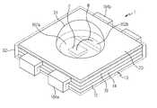
Translated fromKorean도 1은 본 발명의 일 실시예에 따른 LED 패키지를 도시한 사시도.1 is a perspective view showing an LED package according to an embodiment of the present invention.
도 2는 도 1에 도시된 LED 패키지의 단면도.2 is a cross-sectional view of the LED package shown in FIG.
도 3은 하나의 큰 메탈PCB를 베이스로 하여, 다수의 LED 패키지가 제작되는 예를 설명하기 위한 도면.FIG. 3 is a diagram for explaining an example in which a plurality of LED packages are manufactured based on one large metal PCB.
도 4는 본 발명의 다른 실시예에 따른 LED 패키지를 도시한 사시도.4 is a perspective view showing an LED package according to another embodiment of the present invention.
<도면의 주요부분에 대한 부호설명><Code Description of Main Parts of Drawing>
2: LED칩 10: 메탈PCB2: LED chip 10: metal PCB
16: 제 1 금속박판 14: 절연층16: first metal sheet 14: insulating layer
12: 제 2 금속박판 31: 봉지부재12: second metal sheet 31: sealing member
32: 봉지부재의 확장부 20: 홀컵32: expansion part of the sealing member 20: hole cup
162a, 162b: 전극패턴 164a, 164b: 리드162a and 162b:
165a, 165b, 비아 통전부 121, 122 단자패턴165a, 165b, via
본 발명은 LED 패키지에 관한 것으로서, 더욱 상세하게는, 메탈PCB를 갖는 LED 패키지에 관한 것이다.The present invention relates to an LED package, and more particularly, to an LED package having a metal PCB.
일반적으로, LED(Light Emitting Diode)는 전류 인가에 의해 P-N 반도체 접합(P-N junction)에서 전자와 정공이 만나 빛을 발하는 소자로서, 통상, LED칩이 탑재된 패키지의 구조로 제작되며, 흔히, 'LED 패키지'라고 칭해지고 있다. 위와 같은 LED 패키지는 일반적으로 인쇄회로기판(PCB; Printed Circuit Board) 상에 장착되어 그 인쇄회로기판에 형성된 전극으로부터 전류를 인가받아 발광 동작하도록 구성된다.In general, a light emitting diode (LED) is a device in which electrons and holes meet and emit light at a PN semiconductor junction by application of current, and are generally manufactured in a package structure in which an LED chip is mounted. LED package. The LED package as described above is generally mounted on a printed circuit board (PCB) and configured to emit light by receiving a current from an electrode formed on the printed circuit board.
LED 패키지에 있어서, LED칩으로부터 발생한 열은 LED 패키지의 발광 성능 및 수명에 직접적인 영향을 미친다. 그 이유는 LED칩에 발생한 열이 그 LED칩에 오래 머무르는 경우 LED칩을 이루는 결정 구조에 전위(dislocation) 및 부정합(mismatch)를 일으키기 때문이다. 게다가, 근래에는 고출력의 LED 패키지가 개발된 바 있는데, 이러한 고출력의 LED 패키지는, 고전압의 전력에 의해 동작되고 그 고전압에 의해 LED칩에서 많은 열이 발생되므로, 그 발생된 열을 효과적으로 방출시키기 위한 별도의 장치가 요구된다.In the LED package, heat generated from the LED chip directly affects the light emitting performance and lifetime of the LED package. This is because heat generated in an LED chip causes dislocations and mismatches in the crystal structure of the LED chip when the LED chip stays in the LED chip for a long time. In addition, in recent years, high power LED packages have been developed. Since the high power LED packages are operated by high voltage power and generate a lot of heat from the LED chips due to the high voltage, A separate device is required.
이에 대하여, 종래에는 알루미늄 베이스 상에 절연층 및 금속 패턴층이 차례로 형성된 메탈PCB를 이용하여 방열성을 향상시킨 LED 패키지가 개발된 바 있다. 이러한 종래의 LED 패키지는, 예를 들면, 절삭 가공 등의 홈 가공을 통해 알루미늄 베이스의 일부를 상부로 노출시킨 홀컵을 형성하고, 그 홀컵에 LED칩을 부착한 후, LED칩과 금속 패턴층을 도전성 와이어로 연결하여 제조된다.In contrast, conventionally, an LED package having improved heat dissipation by using a metal PCB in which an insulating layer and a metal pattern layer are sequentially formed on an aluminum base has been developed. In such a conventional LED package, for example, a hole cup is formed by exposing a part of the aluminum base to the upper part through groove processing such as cutting, and after attaching the LED chip to the hole cup, the LED chip and the metal pattern layer are formed. It is manufactured by connecting with conductive wires.
그러나, 위와 같은 종래의 LED 패키지는, 알루미늄 베이스의 큰 두께로 인하 여 컴팩트한 구조로 제작하는 것이 힘들고, 외부 전극과 LED칩을 전기적으로 연결시키는 리드 구조를 포함하고 있지 못하여, 통상적으로 이용되는 인쇄회로기판 상에 탑재하는 것이 어려운 문제점이 있다. 이는 종래의 LED 패키지가 기존 전자기기 또는 조명기기와의 호환성이 크게 떨어짐을 의미한다. 또한, 현재의 LED 패키지 제조업체가 리드 구조를 포함하는 LED 패키지 제조에 적합한 설비들을 주로 보유하므로, 위 종래의 LED 패키지는 전술한 것과 같은 기존 설비의 사용을 제한하므로 비경제적이라는 문제점을 또한 갖고 있다.However, the conventional LED package as described above is difficult to produce a compact structure due to the large thickness of the aluminum base, and does not include a lead structure for electrically connecting the external electrode and the LED chip, and is commonly used printing It is difficult to mount on a circuit board. This means that the conventional LED package is greatly incompatible with the existing electronics or lighting equipment. In addition, since the current LED package manufacturers mainly have equipment suitable for manufacturing the LED package including the lead structure, the conventional LED package also has a problem that it is uneconomical because it restricts the use of the existing equipment as described above.
추가로, 종래의 LED 패키지는, 절삭 가공 등과 같은 홈 가공에 의해 홀컵이 형성되므로, 그 홈 가공에 의해 LED칩의 실장면이 불규칙하게 되고, 그것에 의해, LED칩의 다이 어태칭 공정을 어렵게 하며, 또한, 다이 어태칭된 LED칩이 열 충격과 기계적 충격에 쉽게 손상되는 문제점을 야기한다.In addition, in the conventional LED package, since the hole cup is formed by grooving such as cutting, the mounting surface of the LED chip becomes irregular by the grooving, thereby making the die attaching process of the LED chip difficult. In addition, the die-attached LED chip causes a problem of being easily damaged by thermal shock and mechanical shock.
따라서, 본 발명의 기술적 과제는, 방열성과 콤팩트한 구조를 가지며, 기존 설비의 사용을 크게 제한하지 않고, 현재 널리 이용되는 전자기기 또는 조명기기와의 호환성도 좋은, 메탈PCB를 갖는 LED 패키지를 제공하는데에 있다.Accordingly, the technical problem of the present invention is to provide an LED package having a metal PCB, which has a heat dissipation property and a compact structure, and does not greatly limit the use of existing equipment, and also has good compatibility with electronic devices or lighting devices that are widely used at present. It is in
본 발명의 일 측면에 따른 LED 패키지는, 전기 절연층을 사이에 개재한 채 제 1 및 제 2 금속박판을 적층하여 형성된 메탈PCB와, 상기 메탈PCB의 상기 제 1 금속박판에 실장되는 LED칩을 포함하며, 상기 제 1 금속박판은, 전극패턴들과, 상기 전극패턴들로부터 각각 연장된 리드들로 구성된다.The LED package according to an aspect of the present invention, the metal PCB formed by laminating the first and second metal thin plates with an electrical insulation layer interposed therebetween, and the LED chip mounted on the first metal thin plate of the metal PCB. The first metal thin plate may include electrode patterns and leads extending from the electrode patterns, respectively.
이때, 상기 리드들 각각은 상기 메탈PCB로부터 측면 외측 방향으로 연장된 상기 제 1 금속박판의 일부를 절곡하여 형성되는 것이 바람직하다. 더욱 바람직하게는, 상기 리드들 각각은 상기 제 1 금속박판의 일부를 2단으로 중첩 절곡하여 이루어지며, 이에 의해, 상기 리드들 각각은 외부 전극과의 접촉 면적이 확장될 수 있다.In this case, each of the leads is preferably formed by bending a portion of the first metal plate extending in the lateral outward direction from the metal PCB. More preferably, each of the leads is formed by overlapping and bending a portion of the first metal sheet in two stages, whereby each of the leads can have an extended contact area with an external electrode.
대안적으로, 상기 리드들 각각은, 상기 전극패턴들에 상응하게 상기 제 2 금속박판을 패터닝 하여 형성된 단자패턴들과,상기 메탈PCB를 관통하여, 상기 전극패턴들과 상기 단자패턴들을 잇는 비아 통전부를 포함하여 이루어질 수 있다.Alternatively, each of the leads may include terminal patterns formed by patterning the second metal thin plate corresponding to the electrode patterns, and a via tube connecting the electrode patterns and the terminal patterns through the metal PCB. It may be included in all.
본 발명의 바람직한 실시예에 따라, 상기 제 1 및 제 2 금속박판은 구리 또는 구리 합금으로 이루어진다. 또한, 상기 LED 패키지는, 상기 LED칩을 덮도록 상기 제 1 금속박판 상에 형성된 봉지부재를 더 포함하며, 또한, 상기 LED칩으로부터 나온 광의 지향각 조절을 위해 상기 LED칩 주변에 설치되는 홀컵을 추가로 포함할 수 있다. 상기 홀컵은, 수지, 금속, 세라믹 또는 그것들의 복합물을 이용하여 형성되는 것으로, FR4 재질로 이루어질 수 있다. 또한 상기 홀컵은 개구부를 각각 구비한 채 상기 제 1 금속박판 상에 차례대로 형성되는 절연판과 금속 반사판으로 이루어질 수 있다. 그리고, 상기 금속 반사판은 알루미늄으로 이루어지는 것이 바람직하다.According to a preferred embodiment of the present invention, the first and second metal sheets are made of copper or copper alloy. The LED package further includes an encapsulation member formed on the first metal plate to cover the LED chip, and further includes a hole cup installed around the LED chip to adjust a direction angle of light emitted from the LED chip. It may further comprise. The hole cup is formed using a resin, a metal, a ceramic, or a composite thereof, and may be made of a FR4 material. In addition, the hole cup may be formed of an insulating plate and a metal reflecting plate which are sequentially formed on the first metal sheet with openings respectively. The metal reflector is preferably made of aluminum.
이하 첨부된 도면을 참조로 하여 본 발명의 바람직한 실시예를 설명하기로 한다.Hereinafter, exemplary embodiments of the present invention will be described with reference to the accompanying drawings.
실시예Example
도 1은 본 발명의 일 실시예에 따른 LED 패키지를 도시한 사시도이고, 도 2는 도 1에 도시된 LED 패키지의 단면도이다.1 is a perspective view showing an LED package according to an embodiment of the present invention, Figure 2 is a cross-sectional view of the LED package shown in FIG.
도 1 및 도 2에 도시된 것과 같이, 본 실시예의 LED 패키지(1)는, 메탈PCB(10)와, 상기 메탈PCB(10)에 실장되는 LED칩(2) 등을 포함한다. 그리고, 상기 메탈PCB(10)에는 상기 LED칩(2)을 보호하기 위한 광투과성의 봉지부재(31)가 대략 반구형으로 형성된다. 그리고, 상기 봉지부재(31)는, 그와 일체로 확장 형성되어, 상기 메탈PCB(10)의 상면 및 측면 일부를 덮는 확장부(32)를 더 포함하며, 그 확장부(32)에 의해, 상기 LED칩(2)은 물론이고 상기 메탈PCB(10)까지 외부로부터 보호할 수 있다.As shown in FIG. 1 and FIG. 2, the LED package 1 of the present embodiment includes a
본 실시예에 따른 메탈PCB(10)는 제 1 및 제 2 금속박판(16, 12)과, 그 금속박판들(16, 12) 사이에 개재된 절연층(14)을 포함하되, 상기 제 1 및 제 2 금속박판(16, 12)은 상기 절연층(14)을 사이에 두고 적층되어 있다. 상기 제 2 금속박판(12)은 구리 또는 구리 합금으로 이루어진 채 상기 메탈PCB(10)의 베이스를 이루며, 상기 제 1 금속박판(16)은 구리 또는 구리 합금으로 이루어진 채 상기 절연층(14)에 의해 상기 제 2 금속박판(12)과 전기적으로 절연되어 있다.The
상기 제 1 금속박판(16)은, 상기 LED칩(2)이 부착되는 제 1 전극패턴(162a)과, 그 제 1 전극패턴(162a)으로부터 이격되도록 패터닝된 제 2 전극패턴(162b)을 포함하며, 상기 제 1 전극패턴(162a) 상의 LED칩(2)은 본딩와이어(W)에 의해 상기 제 2 전극패턴(162b)과 전기적으로 연결된다. 이때, 상기 절연층(14)은 전기적으로 절연성을 갖되, 상기 LED칩(2)으로부터 발생한 열의 원할한 방출을 위해, 열전도성 이 좋은 소재로 형성되는 것이 바람직하다.The first metal
본 발명의 실시예에 따라, 상기 제 1 금속박판(16)은 상기 메탈PCB(10)의 측면 외측 방향으로 연장된 리드들(164a, 164b)을 더 포함한다. 상기 리드들(164a, 164b)은 LED 패키지(1)가 장착되는 외부 인쇄회로기판(미도시됨) 상의 외부 전극들에 연결되는 부분으로, 2단 중첩 절곡에 의해, 아래쪽으로 배향됨과 동시에 외부 전극(미도시됨)과의 넓은 접촉 면적을 갖게 된다. 즉, 상기 리드들(164a, 164b) 각각은 첫 번째 절곡에 의해 아래쪽으로 배향되고 두 번째 절곡에 의해 면들끼리 중첩되어 제 1 금속박판(16)의 실제 두께에 비해 큰 두께의 단부를 갖게 된다.According to the exemplary embodiment of the present invention, the first metal
도 1 및 도 2에 도시된 LED 패키지(1)가, 리드들(164a, 164b)의 절곡 위치 및 방향에 의해, 패키지 장착면과 광 방출면이 서로 반대되게 위치한 탑 뷰(top view) 타입이지만, 상기 리드들(164a, 164b)의 절곡 위치 및 방향을 달리하여, 패키지 장착면과 광 방출면이 수직을 이루도록 하는 것도 고려될 수 있으며, 이와 같이, 패키지 장착면과 광 방출면이 수직을 이루는 구조는 통상 사이드 뷰(side view) 타입으로 칭해지는 LED 패키지의 구현에 적합하다.Although the LED package 1 shown in FIGS. 1 and 2 is a top view type in which the package mounting surface and the light emitting surface are opposite to each other by the bending positions and directions of the
또한, 본 실시예에 따른 LED 패키지(1)는 원하는 광 지향각을 얻기 위한, 즉, LED칩(2)으로부터 나온 광의 지향각 조절을 위한 홀컵(20)을 더 포함한다. 상기 홀컵(20)은, 상기 봉지부재(31)의 일부가 충전되는 개구부를 포함하는 것으로, 상기 제 1 금속박판(16) 상에서 상기 LED칩(2) 주변을 둘러싸서 광을 원하는 지향각 범위 내로 반사시키는 역할을 한다. 상기 홀컵(20)은, 상기 메탈PCB(10)의 제 1 금속박판(16) 상에 직접 적층되어 형성되므로, 메탈PCB에 홈을 가공하여 홀컵을 형 성할 필요성을 없애주며, 따라서, 종래의 기술과 달리, 메탈PCB의 칩 실장면이 평탄하게 형성된다.In addition, the LED package 1 according to the present embodiment further includes a
본 발명의 실시예에 따라, 상기 홀컵(20)은 판 형상의 부재에 개구부를 형성한 것이 이용될 수 있으며, 그 재질은, 수지, 금속, 세라믹 또는 그것들의 복합물일 수 있다. 일 예로, 상기 홀컵(20)으로는 FR4와 같은 소재가 이용될 수 있는데, 상기 FR4는 유리섬유를 에폭시와 결합하여 보강한 소재(약어로, ERBGF; Epoxy Resin Bonded Glass Fiber)로써 강도와 광 반사성이 좋으며, 통상 인쇄회로기판의 원자재로 이용되고 있다.According to the exemplary embodiment of the present invention, the
다른 예로써, 상기 홀컵(20)은, 도 2의 확대도에 도시한 것과 같이, 개구부들이 각각 형성되고 서로 접합되어 있는 절연판(21)과 금속 반사판(22)에 의해 형성될 수 있다. 이때, 상기 절연판(21)은 그 아래쪽에 위치한 제 1 금속박판(16)과 상기 금속 반사판(22) 사이를 전기적으로 절연시키는 역할을 한다. 또한, 상기 금속 반사판(22)은 알루미늄 소재로 이루어지는 것이 바람직하다.As another example, as shown in the enlarged view of FIG. 2, the
본 발명의 실시예에 따라, 전술한 메탈PCB(10)는 도 3에 도시된 하나의 큰 메탈PCB(10'; 이하, '적층 원자재'라 함)로부터 절단 분리된 단위 메탈PCB(10)이며, 그 메탈PCB(10)를 포함하는 다수의 LED 패키지(1)들은, 도 3에 도시된 것과 같이, 상기 적층 원자재(10')를 베이스로 하여 미리 형성된다. 상기 적층 원자재(10')는 미리 정해진 형상으로 패터닝 가공된 제 1 금속박판(16), 절연층(14), 제 2 금속박판(12)의 적층물이며, 상기 제 1 금속박판(16)으로부터 연장된 리드들(164a, 164b)과 각 층들의 지지부(102')들에 의해, 다수의 LED 패키지(1)들이 상 기 적층 원자재(10')에 지지된다. 그리고, 상기 지지부(102')들과 상기 리드들(164a, 164b)를 절단하고, 그 리드들(164a, 164b)을 앞서 설명한 것과 같이 절곡하면 도 1 및 도 2에 도시된 구조를 갖는 단위 LED 패키지(1)들이 된다.According to an embodiment of the present invention, the above-described
도 4는 본 발명의 다른 실시예에 따른 LED 패키지(1)를 도시한 단면도이다. 본 실시예의 LED 패키지(1)는 제 1 금속박판(16)의 전극패턴들(162a, 162b)로부터 연장된 리드의 구조를 제외하면 나머지 구성이 앞선 실시예와 실질적으로 같으며, 따라서, 이하에서는, 앞선 실시예와 달라진 리드의 구조에 대해서 주로 설명하기로 한다.4 is a cross-sectional view showing an LED package 1 according to another embodiment of the present invention. The LED package 1 of the present embodiment is substantially the same as the previous embodiment except for the structure of the lead extending from the
도 4에 도시된 것과 같이, 본 실시예의 리드들은, 제 1 금속박판(16)의 전극패턴들(162a, 162b)에 상응하게 제 2 금속박판(12)을 패터닝 하여 형성된 단자패턴들(121, 122)과,상기 메탈PCB(10)를 관통하여, 상기 전극패턴들(162a, 162b)과 상기 단자패턴(121, 122)들을 잇는 비아(via) 통전부(165a, 165b)를 포함한다. 이때, 상기 비아 통전부(165a, 165b)는 상기 메탈PCB(10)를 상하로 관통하는 개구부들을 미리 형성한 후, 예를 들면, 도금 등의 방식으로 상기 개구부들에 상기 제 1 금속박판(16) 및/또는 제 2 금속박판(12)과 동일한 소재의 금속을 채워 넣는 것에 의해 형성될 수 있는 것이다.As shown in FIG. 4, the leads of the present exemplary embodiment may include
이상에서는 본 발명이 특정 실시예를 중심으로 하여 설명되었지만, 본 발명의 취지 및 첨부된 특허청구범위 내에서 다양한 변형, 변경 또는 수정이 당해 기술분야에서 있을 수 있으며, 따라서, 전술한 설명 및 도면은 본 발명의 기술사상을 한정하는 것이 아닌 본 발명을 예시하는 것으로 해석되어져야 한다.While the invention has been described above with reference to specific embodiments, various modifications, changes or modifications may be made in the art within the spirit and scope of the appended claims, and thus, the foregoing description and drawings It should be construed as illustrating the present invention rather than limiting the technical spirit of the present invention.
본 발명에 따른 LED 패키지는, 충분한 방열성과 함께 컴팩트한 구조를 가지며, 메탈PCB를 이용하면서도, 일반적인 LED 패키지와 대략 동일한 구조를 가진 채 외부 전극과 연결되는 리드들을 포함하여 기존 전자기기 또는 조명기기와의 호환성이 좋다는 이점이 있다. 게다가, 본 발명에 따른 LED 패키지는, 그것의 제작 공정이 메탈PCB를 포함하지 않는 일반적인 LED 패키지와 제작 공정과 상당 부분 같아, 현 LED 패키지 제조업체에서 보유하고 있는 많은 설비를 그대로 이용할 수 있게 해주는 경제적인 이점 또한 갖는다. 또한, 본 발명에 따른 LED 패키지는, LED칩이 위치하는 홀컵 형성을 위해 별도의 홈 가공이 요구되지 않으므로, 평탄한 칩 실장면을 가지며, 이에 의해, LED칩의 다이 어태칭 공정이 종래 메탈PCB형 LED 패키지에 비해 용이하고, 또한, 다이 어태칭된 LED칩이 열 충격과 기계적 충격에 강하다는 이점을 갖는다.The LED package according to the present invention has a compact structure with sufficient heat dissipation, and uses a metal PCB, and includes the leads connected to the external electrode while having a structure substantially the same as that of a general LED package. Has the advantage of good compatibility. In addition, the LED package according to the present invention is much the same as the general LED package and the manufacturing process that does not include a metal PCB, so that it is economical to use many of the facilities possessed by the current LED package manufacturers. There is also an advantage. In addition, since the LED package according to the present invention does not require a separate groove for forming a hole cup in which the LED chip is located, the LED package has a flat chip mounting surface, whereby the die attaching process of the LED chip is performed by a conventional metal PCB type. Compared to the LED package, it is easier and also has the advantage that the die-attached LED chip is resistant to thermal shock and mechanical shock.
Claims (12)
Translated fromKoreanPriority Applications (5)
| Application Number | Priority Date | Filing Date | Title |
|---|---|---|---|
| KR1020070032018AKR100850666B1 (en) | 2007-03-30 | 2007-03-30 | LED package with metal PC |
| JP2008086946AJP2008258617A (en) | 2007-03-30 | 2008-03-28 | LED package with metal PCB |
| US12/058,417US7642563B2 (en) | 2007-03-30 | 2008-03-28 | LED package with metal PCB |
| US12/623,978US8138512B2 (en) | 2007-03-30 | 2009-11-23 | LED package with metal PCB |
| JP2013112983AJP5706469B2 (en) | 2007-03-30 | 2013-05-29 | LED package with metal PCB |
Applications Claiming Priority (1)
| Application Number | Priority Date | Filing Date | Title |
|---|---|---|---|
| KR1020070032018AKR100850666B1 (en) | 2007-03-30 | 2007-03-30 | LED package with metal PC |
Publications (1)
| Publication Number | Publication Date |
|---|---|
| KR100850666B1true KR100850666B1 (en) | 2008-08-07 |
Family
ID=39792671
Family Applications (1)
| Application Number | Title | Priority Date | Filing Date |
|---|---|---|---|
| KR1020070032018AExpired - Fee RelatedKR100850666B1 (en) | 2007-03-30 | 2007-03-30 | LED package with metal PC |
Country Status (3)
| Country | Link |
|---|---|
| US (2) | US7642563B2 (en) |
| JP (2) | JP2008258617A (en) |
| KR (1) | KR100850666B1 (en) |
Cited By (6)
| Publication number | Priority date | Publication date | Assignee | Title |
|---|---|---|---|---|
| KR101108984B1 (en)* | 2009-12-03 | 2012-01-31 | (주) 아모엘이디 | Multichip LED Package and Manufacturing Method Thereof |
| WO2014196833A1 (en)* | 2013-06-07 | 2014-12-11 | 서울반도체 주식회사 | Light-emitting device |
| KR101637328B1 (en)* | 2015-03-30 | 2016-07-07 | 주식회사 루멘스 | Light emitting device package and lighting device |
| CN109216516A (en)* | 2017-06-30 | 2019-01-15 | 英属开曼群岛商錼创科技股份有限公司 | Micro-led and display panel |
| KR102032419B1 (en) | 2019-03-11 | 2019-10-15 | 주식회사 제이케이테크원 | Copper based metal PCB |
| KR20200130013A (en)* | 2019-05-10 | 2020-11-18 | 주식회사 옵티맥 | A LED module package |
Families Citing this family (27)
| Publication number | Priority date | Publication date | Assignee | Title |
|---|---|---|---|---|
| TWI488329B (en)* | 2008-05-15 | 2015-06-11 | Everlight Electronics Co Ltd | Circuit substrate and LED package |
| JP4780203B2 (en)* | 2009-02-10 | 2011-09-28 | 日亜化学工業株式会社 | Semiconductor light emitting device |
| TWI380486B (en) | 2009-03-02 | 2012-12-21 | Everlight Electronics Co Ltd | Heat dissipation module for a light emitting device and light emitting diode device having the same |
| JP5574667B2 (en)* | 2009-10-21 | 2014-08-20 | キヤノン株式会社 | Package, semiconductor device, manufacturing method and equipment thereof |
| KR200462269Y1 (en) | 2010-03-30 | 2012-09-03 | 에스디아이 코퍼레이션 | Luminous device package frame with an improved reliability |
| US8519426B2 (en) | 2010-08-09 | 2013-08-27 | Lg Innotek Co., Ltd. | Light emitting device and lighting system having the same |
| KR101626412B1 (en)* | 2010-12-24 | 2016-06-02 | 삼성전자주식회사 | Light emitting device package and method of manufacturing the same |
| CN102163600A (en)* | 2010-12-31 | 2011-08-24 | 东莞市万丰纳米材料有限公司 | LED package module |
| CN102163599A (en)* | 2010-12-31 | 2011-08-24 | 东莞市万丰纳米材料有限公司 | LED package module |
| KR101825473B1 (en)* | 2011-02-16 | 2018-02-05 | 삼성전자 주식회사 | Light emitting device package and method of fabricating the same |
| KR101846356B1 (en)* | 2011-07-29 | 2018-04-09 | 엘지이노텍 주식회사 | Optical component package and manufacturing method thereof |
| KR101846364B1 (en)* | 2011-07-29 | 2018-04-09 | 엘지이노텍 주식회사 | Optical component package and manufacturing method thereof |
| JP2013042079A (en) | 2011-08-19 | 2013-02-28 | Sharp Corp | Semiconductor light emitting device |
| TR201802109T4 (en) | 2011-12-19 | 2018-03-21 | Coca Cola Co | Beverage containing steviol glycosides. |
| CA2867053A1 (en) | 2012-03-12 | 2013-09-19 | Zhejiang Ledison Optoelectronics Co., Ltd. | Led light-emitting column and led light using the same |
| KR20130107536A (en)* | 2012-03-22 | 2013-10-02 | 삼성전자주식회사 | Led pakage and method of manufacturing same |
| CN103366645A (en)* | 2013-03-22 | 2013-10-23 | 美的集团武汉制冷设备有限公司 | Light emitting display device |
| US10016580B2 (en) | 2013-12-17 | 2018-07-10 | Biovision Technologies, Llc | Methods for treating sinus diseases |
| US9510743B2 (en) | 2013-12-17 | 2016-12-06 | Biovision Technologies, Llc | Stabilized surgical device for performing a sphenopalatine ganglion block procedure |
| US9516995B2 (en) | 2013-12-17 | 2016-12-13 | Biovision Technologies, Llc | Surgical device for performing a sphenopalatine ganglion block procedure |
| US9694163B2 (en) | 2013-12-17 | 2017-07-04 | Biovision Technologies, Llc | Surgical device for performing a sphenopalatine ganglion block procedure |
| US9876152B2 (en)* | 2014-05-27 | 2018-01-23 | Epistar Corporation | Light emitting device with an adhered heat-dissipating structure |
| US9829524B2 (en)* | 2015-05-05 | 2017-11-28 | The United States Of America As Represented By The Secretary Of The Army | Electric field sensor |
| US9823718B2 (en) | 2016-01-13 | 2017-11-21 | Microsoft Technology Licensing, Llc | Device cooling |
| JP6857496B2 (en)* | 2016-12-26 | 2021-04-14 | 日亜化学工業株式会社 | Light emitting device |
| WO2020005910A1 (en) | 2018-06-28 | 2020-01-02 | Sandler Scientific, Llc | Sino-nasal rinse delivery device with agitation, flow-control and integrated medication management system |
| CN111463198B (en)* | 2020-05-22 | 2025-08-05 | 松山湖材料实验室 | COB packaging structure of UVC-LED and its manufacturing method |
Citations (2)
| Publication number | Priority date | Publication date | Assignee | Title |
|---|---|---|---|---|
| KR20040092512A (en)* | 2003-04-24 | 2004-11-04 | (주)그래픽테크노재팬 | A semiconductor light emitting device with reflectors having a cooling function |
| KR20070001349A (en)* | 2005-06-29 | 2007-01-04 | 윤성만 | Thermal Package for Light Emitting Diodes |
Family Cites Families (11)
| Publication number | Priority date | Publication date | Assignee | Title |
|---|---|---|---|---|
| JPH03237752A (en)* | 1990-02-15 | 1991-10-23 | Mitsubishi Electric Corp | Electronic part package |
| JPH08139257A (en)* | 1994-11-07 | 1996-05-31 | Hitachi Ltd | Surface mount semiconductor device |
| JP4846087B2 (en)* | 1999-11-01 | 2011-12-28 | ローム株式会社 | Light emitting display device and manufacturing method thereof |
| US7244965B2 (en)* | 2002-09-04 | 2007-07-17 | Cree Inc, | Power surface mount light emitting die package |
| TW578280B (en)* | 2002-11-21 | 2004-03-01 | United Epitaxy Co Ltd | Light emitting diode and package scheme and method thereof |
| JP4633333B2 (en)* | 2003-01-23 | 2011-02-16 | 株式会社光波 | Light emitting device |
| JP4504662B2 (en)* | 2003-04-09 | 2010-07-14 | シチズン電子株式会社 | LED lamp |
| JP4238693B2 (en)* | 2003-10-17 | 2009-03-18 | 豊田合成株式会社 | Optical device |
| JP4645089B2 (en)* | 2004-07-26 | 2011-03-09 | 日亜化学工業株式会社 | Light emitting device and phosphor |
| JP2007013066A (en)* | 2005-07-04 | 2007-01-18 | Element Denshi:Kk | Light emitting device |
| KR100854328B1 (en)* | 2006-07-07 | 2008-08-28 | 엘지전자 주식회사 | Light emitting device package and its manufacturing method |
- 2007
- 2007-03-30KRKR1020070032018Apatent/KR100850666B1/ennot_activeExpired - Fee Related
- 2008
- 2008-03-28JPJP2008086946Apatent/JP2008258617A/ennot_activeWithdrawn
- 2008-03-28USUS12/058,417patent/US7642563B2/enactiveActive
- 2009
- 2009-11-23USUS12/623,978patent/US8138512B2/enactiveActive
- 2013
- 2013-05-29JPJP2013112983Apatent/JP5706469B2/enactiveActive
Patent Citations (2)
| Publication number | Priority date | Publication date | Assignee | Title |
|---|---|---|---|---|
| KR20040092512A (en)* | 2003-04-24 | 2004-11-04 | (주)그래픽테크노재팬 | A semiconductor light emitting device with reflectors having a cooling function |
| KR20070001349A (en)* | 2005-06-29 | 2007-01-04 | 윤성만 | Thermal Package for Light Emitting Diodes |
Cited By (7)
| Publication number | Priority date | Publication date | Assignee | Title |
|---|---|---|---|---|
| KR101108984B1 (en)* | 2009-12-03 | 2012-01-31 | (주) 아모엘이디 | Multichip LED Package and Manufacturing Method Thereof |
| WO2014196833A1 (en)* | 2013-06-07 | 2014-12-11 | 서울반도체 주식회사 | Light-emitting device |
| KR101637328B1 (en)* | 2015-03-30 | 2016-07-07 | 주식회사 루멘스 | Light emitting device package and lighting device |
| CN109216516A (en)* | 2017-06-30 | 2019-01-15 | 英属开曼群岛商錼创科技股份有限公司 | Micro-led and display panel |
| KR102032419B1 (en) | 2019-03-11 | 2019-10-15 | 주식회사 제이케이테크원 | Copper based metal PCB |
| KR20200130013A (en)* | 2019-05-10 | 2020-11-18 | 주식회사 옵티맥 | A LED module package |
| KR102270848B1 (en) | 2019-05-10 | 2021-06-29 | 주식회사 옵티맥 | A LED module package |
Also Published As
| Publication number | Publication date |
|---|---|
| US20080237624A1 (en) | 2008-10-02 |
| JP2008258617A (en) | 2008-10-23 |
| US20100065876A1 (en) | 2010-03-18 |
| US8138512B2 (en) | 2012-03-20 |
| JP2013168682A (en) | 2013-08-29 |
| US7642563B2 (en) | 2010-01-05 |
| JP5706469B2 (en) | 2015-04-22 |
Similar Documents
| Publication | Publication Date | Title |
|---|---|---|
| KR100850666B1 (en) | LED package with metal PC | |
| JP4305896B2 (en) | High brightness light emitting device and manufacturing method thereof | |
| US20080067526A1 (en) | Flexible circuits having improved reliability and thermal dissipation | |
| US10361151B2 (en) | Wiring board having isolator and bridging element and method of making wiring board | |
| JP2013522893A (en) | Film system for use with LEDs | |
| US20130037845A1 (en) | Lead frame, and light emitting diode module having the same | |
| JPWO2006030671A1 (en) | LED device | |
| JP5940799B2 (en) | Electronic component mounting package, electronic component package, and manufacturing method thereof | |
| US20100072502A1 (en) | Light-emitting diode | |
| JP2005158957A (en) | Light emitting device | |
| US6703564B2 (en) | Printing wiring board | |
| RU2423803C2 (en) | Wiring board for electronic component | |
| EP3345464B1 (en) | Method of making an led device | |
| KR101173800B1 (en) | Printed circuit board for light emitting diode and manufacturing method thereof | |
| KR101498682B1 (en) | Light emitting diode module | |
| US20100258838A1 (en) | Packaging substrate device, method for making the packaging substrate device, and packaged light emitting device | |
| KR101115403B1 (en) | Light emitting apparatus | |
| JP4533058B2 (en) | Reflector for lighting device | |
| KR20120005759A (en) | Heat dissipation circuit board and its manufacturing method | |
| JP2012160528A (en) | Semiconductor package | |
| WO2017016863A1 (en) | Integrated led module with ims substrate | |
| KR101523000B1 (en) | 3D lighting device | |
| KR101064013B1 (en) | Light emitting module | |
| KR101768908B1 (en) | Metal printed circuit board and method for manufacturing same and light emitting diode package structure and method for manufacturing same | |
| KR20140097030A (en) | Printed circuit board, optoelectronic component, and assembly of optoelectronic components |
Legal Events
| Date | Code | Title | Description |
|---|---|---|---|
| A201 | Request for examination | ||
| PA0109 | Patent application | St.27 status event code:A-0-1-A10-A12-nap-PA0109 | |
| PA0201 | Request for examination | St.27 status event code:A-1-2-D10-D11-exm-PA0201 | |
| E902 | Notification of reason for refusal | ||
| PE0902 | Notice of grounds for rejection | St.27 status event code:A-1-2-D10-D21-exm-PE0902 | |
| P11-X000 | Amendment of application requested | St.27 status event code:A-2-2-P10-P11-nap-X000 | |
| P13-X000 | Application amended | St.27 status event code:A-2-2-P10-P13-nap-X000 | |
| E701 | Decision to grant or registration of patent right | ||
| PE0701 | Decision of registration | St.27 status event code:A-1-2-D10-D22-exm-PE0701 | |
| GRNT | Written decision to grant | ||
| PR0701 | Registration of establishment | St.27 status event code:A-2-4-F10-F11-exm-PR0701 | |
| PR1002 | Payment of registration fee | St.27 status event code:A-2-2-U10-U11-oth-PR1002 Fee payment year number:1 | |
| PG1601 | Publication of registration | St.27 status event code:A-4-4-Q10-Q13-nap-PG1601 | |
| P22-X000 | Classification modified | St.27 status event code:A-4-4-P10-P22-nap-X000 | |
| PR1001 | Payment of annual fee | St.27 status event code:A-4-4-U10-U11-oth-PR1001 Fee payment year number:4 | |
| PR1001 | Payment of annual fee | St.27 status event code:A-4-4-U10-U11-oth-PR1001 Fee payment year number:5 | |
| FPAY | Annual fee payment | Payment date:20130604 Year of fee payment:6 | |
| PR1001 | Payment of annual fee | St.27 status event code:A-4-4-U10-U11-oth-PR1001 Fee payment year number:6 | |
| FPAY | Annual fee payment | Payment date:20140619 Year of fee payment:7 | |
| PR1001 | Payment of annual fee | St.27 status event code:A-4-4-U10-U11-oth-PR1001 Fee payment year number:7 | |
| FPAY | Annual fee payment | Payment date:20150608 Year of fee payment:8 | |
| PR1001 | Payment of annual fee | St.27 status event code:A-4-4-U10-U11-oth-PR1001 Fee payment year number:8 | |
| PN2301 | Change of applicant | St.27 status event code:A-5-5-R10-R13-asn-PN2301 St.27 status event code:A-5-5-R10-R11-asn-PN2301 | |
| R18-X000 | Changes to party contact information recorded | St.27 status event code:A-5-5-R10-R18-oth-X000 | |
| FPAY | Annual fee payment | Payment date:20160601 Year of fee payment:9 | |
| PR1001 | Payment of annual fee | St.27 status event code:A-4-4-U10-U11-oth-PR1001 Fee payment year number:9 | |
| PR1001 | Payment of annual fee | St.27 status event code:A-4-4-U10-U11-oth-PR1001 Fee payment year number:10 | |
| PR1001 | Payment of annual fee | St.27 status event code:A-4-4-U10-U11-oth-PR1001 Fee payment year number:11 | |
| FPAY | Annual fee payment | Payment date:20190701 Year of fee payment:12 | |
| PR1001 | Payment of annual fee | St.27 status event code:A-4-4-U10-U11-oth-PR1001 Fee payment year number:12 | |
| PR1001 | Payment of annual fee | St.27 status event code:A-4-4-U10-U11-oth-PR1001 Fee payment year number:13 | |
| PC1903 | Unpaid annual fee | St.27 status event code:A-4-4-U10-U13-oth-PC1903 Not in force date:20210801 Payment event data comment text:Termination Category : DEFAULT_OF_REGISTRATION_FEE | |
| PC1903 | Unpaid annual fee | St.27 status event code:N-4-6-H10-H13-oth-PC1903 Ip right cessation event data comment text:Termination Category : DEFAULT_OF_REGISTRATION_FEE Not in force date:20210801 | |
| P22-X000 | Classification modified | St.27 status event code:A-4-4-P10-P22-nap-X000 |