KR100850516B1 - Flash memory device and program method thereof - Google Patents
Flash memory device and program method thereofDownload PDFInfo
- Publication number
- KR100850516B1 KR100850516B1KR1020070008024AKR20070008024AKR100850516B1KR 100850516 B1KR100850516 B1KR 100850516B1KR 1020070008024 AKR1020070008024 AKR 1020070008024AKR 20070008024 AKR20070008024 AKR 20070008024AKR 100850516 B1KR100850516 B1KR 100850516B1
- Authority
- KR
- South Korea
- Prior art keywords
- voltage
- program
- bulk region
- high voltage
- memory cells
- Prior art date
- Legal status (The legal status is an assumption and is not a legal conclusion. Google has not performed a legal analysis and makes no representation as to the accuracy of the status listed.)
- Expired - Fee Related
Links
Images


Classifications
- G—PHYSICS
- G11—INFORMATION STORAGE
- G11C—STATIC STORES
- G11C16/00—Erasable programmable read-only memories
- G11C16/02—Erasable programmable read-only memories electrically programmable
- G11C16/06—Auxiliary circuits, e.g. for writing into memory
- G11C16/10—Programming or data input circuits
- G—PHYSICS
- G11—INFORMATION STORAGE
- G11C—STATIC STORES
- G11C16/00—Erasable programmable read-only memories
- G11C16/02—Erasable programmable read-only memories electrically programmable
- G11C16/04—Erasable programmable read-only memories electrically programmable using variable threshold transistors, e.g. FAMOS
- G11C16/0483—Erasable programmable read-only memories electrically programmable using variable threshold transistors, e.g. FAMOS comprising cells having several storage transistors connected in series
- G—PHYSICS
- G11—INFORMATION STORAGE
- G11C—STATIC STORES
- G11C16/00—Erasable programmable read-only memories
- G11C16/02—Erasable programmable read-only memories electrically programmable
- G11C16/06—Auxiliary circuits, e.g. for writing into memory
- G11C16/10—Programming or data input circuits
- G11C16/12—Programming voltage switching circuits
- G—PHYSICS
- G11—INFORMATION STORAGE
- G11C—STATIC STORES
- G11C16/00—Erasable programmable read-only memories
- G11C16/02—Erasable programmable read-only memories electrically programmable
- G11C16/06—Auxiliary circuits, e.g. for writing into memory
- G11C16/30—Power supply circuits
- G—PHYSICS
- G11—INFORMATION STORAGE
- G11C—STATIC STORES
- G11C16/00—Erasable programmable read-only memories
- G11C16/02—Erasable programmable read-only memories electrically programmable
- G11C16/06—Auxiliary circuits, e.g. for writing into memory
- G11C16/34—Determination of programming status, e.g. threshold voltage, overprogramming or underprogramming, retention
- G11C16/3436—Arrangements for verifying correct programming or erasure
- G11C16/3454—Arrangements for verifying correct programming or for detecting overprogrammed cells
Landscapes
- Engineering & Computer Science (AREA)
- Microelectronics & Electronic Packaging (AREA)
- Read Only Memory (AREA)
Abstract
Translated fromKorean
Description
Translated fromKorean도 1은 본 발명의 임베디드 낸드 플래시 메모리 장치를 구비한 스마트 카드의 구성을 간략히 보여주는 블록도;1 is a block diagram schematically showing a configuration of a smart card having an embedded NAND flash memory device of the present invention;
도 2는 도 1의 임베디드 낸드 플래시 메모리 장치를 개략적으로 보여주는 블록도;FIG. 2 is a block diagram schematically illustrating an embedded NAND flash memory device of FIG. 1; FIG.
도 3은 본 발명의 제 1 실시예에 따른 임베디드 낸드 플래시 메모리 장치의 프로그램 방법을 설명하는 순서도;3 is a flowchart illustrating a program method of an embedded NAND flash memory device according to a first embodiment of the present invention;
도 4는 도 3의 동작에 따른 바이어스 상태들을 간략히 보여주는 파형도;4 is a waveform diagram schematically illustrating bias states according to the operation of FIG. 3;
도 5는 본 발명의 제 2 실시예에 따른 임베디드 낸드 플래시 메모리 장치의 프로그램 방법을 설명하는 순서도;5 is a flowchart illustrating a program method of an embedded NAND flash memory device according to a second embodiment of the present invention;
도 6은 도 5의 동작에 따른 바이어스 상태들을 간략히 보여주는 파형도;6 is a waveform diagram schematically illustrating bias states according to the operation of FIG. 5;
도 7은 본 발명의 제 3 실시예에 따른 임베디드 낸드 플래시 메모리 장치의 프로그램 방법을 설명하는 순서도;7 is a flowchart illustrating a program method of an embedded NAND flash memory device according to a third embodiment of the present invention;
도 8은 본 발명의 제 4 실시예에 따른 임베디드 낸드 플래시 메모리 장치의 프로그램 방법을 설명하는 순서도.8 is a flowchart illustrating a program method of an embedded NAND flash memory device according to a fourth embodiment of the present invention.
*도면의 주요 부분에 대한 부호의 설명** Description of the symbols for the main parts of the drawings *
10 : 임베디드 노어 플래시 메모리10: embedded NOR flash memory
20 : 임베디드 낸드 플래시 메모리20: embedded NAND flash memory
30 : 램40 : 메모리 블록30: RAM 40: Memory Block
50 : 고전압 발생기60 : 중앙처리장치50: high voltage generator 60: central processing unit
70 : 보안 회로80 : 인터페이스 회로70: security circuit 80: interface circuit
100 : 전압 레귤레이터110 : 행 디코더100: voltage regulator 110: row decoder
120 : 셀 어레이130 : 페이지 버퍼120: cell array 130: page buffer
140 : 프로그램 제어부140: program control unit
본 발명은 반도체 메모리 장치에 관한 것으로, 좀 더 구체적으로는 임베디드 플래시 메모리 장치 및 그것의 프로그램 방법에 관한 것이다.The present invention relates to a semiconductor memory device, and more particularly to an embedded flash memory device and a program method thereof.
최근 들어, 모바일 기기들은 휴대하기 용이하도록 제품의 경박단소화가 경쟁적으로 진행되고 있다. 또한, 스마트 카드나 RFID 태그에 사용되는 반도체 칩은 하나의 칩 내부에서 다양한 기능들을 구현할 수 있어야 한다. 따라서, 휴대용 단말기나 스마트 카드에 사용되는 반도체 칩들에서는 CPU, DSP, 메모리 등을 하나의 칩 상에 구현하는 SoC(System-on-Chip: 이하 SoC) 기술이 채용되고 있다. 휴대용 단말기 등의 SoC에 탑재된 메모리는 DRAM, SRAM 뿐만 아니라 플래시 메모리와 같은 불휘발성 메모리를 포함한다. 휘발성 반도체 메모리 장치는 읽고 쓰는 속도가 빠르지 만 외부 전원 공급이 끊기면 저장된 내용이 사라져 버리는 단점이 있다. 반면에 불휘발성 반도체 메모리 장치는 외부 전원 공급이 중단되더라도 그 내용을 보존한다. 그러므로, 불휘발성 반도체 메모리 장치는 전원의 공급 여부에 관계없이 보존되어야 할 내용(예를 들면, 부트 코드 등)을 기억시키는 데 쓰인다. 일반적으로 SoC에 탑재된 플래시 메모리는 속도가 빠른 노어형 플래시 메모리가 주로 사용되어 오고 있다. 노어형 플래시 메모리는 고속 동작 특성을 갖는 반면에 고집적화에 상대적으로 취약하다는 단점이 있다.In recent years, the mobile device has been in a light and small size of the product competitively to be easy to carry. In addition, semiconductor chips used in smart cards or RFID tags should be able to implement various functions in one chip. Accordingly, in semiconductor chips used in portable terminals and smart cards, a system-on-chip (SoC) technology for implementing a CPU, a DSP, a memory, and the like on one chip is adopted. The memory mounted on SoCs of portable terminals and the like includes DRAM, SRAM, as well as nonvolatile memory such as flash memory. The volatile semiconductor memory device has a high reading and writing speed, but the stored content disappears when the external power supply is cut off. On the other hand, nonvolatile semiconductor memory devices retain their contents even when the external power supply is interrupted. Therefore, the nonvolatile semiconductor memory device is used to store contents (for example, boot codes, etc.) to be preserved regardless of whether power is supplied or not. In general, flash memory mounted in SoC has been mainly used for fast NOR flash memory. NOR-type flash memory has a high operating speed, but has a disadvantage of being relatively vulnerable to high integration.
상술한 경박단소화의 트렌드(Trend)와 함께, 모바일 기기나 스마트 카드 분야에서 고집적 요구가 날로 증가하고 있다. 특히 스마트 카드의 경우, 하나의 칩에 고속으로 데이터를 기입/독출해야 할 필요성과, 고용량의 데이터 저장에 대한 필요성을 모두 충족시키기 위한 연구가 활발히 진행되고 있다. 상술한 고속/고용량을 모두 만족하기 위한 시도 중의 하나가 낸드 플래시 메모리를 스마트 카드의 칩에 형성(Embed)하는 것이다. 이하에서는 이러한 낸드형 플래시 메모리를 임베디드 낸드 플래시(Embeded NAND Flash)라 칭하기로 한다.Along with the trend of light and short, the high integration demand is increasing day by day in the field of mobile devices and smart cards. In particular, in the case of a smart card, studies are being actively conducted to satisfy both the need to write / read data at a high speed on a single chip and the need for high capacity data storage. One of the attempts to satisfy both the high speed and high capacity described above is to embed a NAND flash memory in a chip of a smart card. Hereinafter, such a NAND flash memory will be referred to as an embedded NAND flash.
하지만, 일반적인 낸드형 플래시 메모리와 노어형 플래시 메모리의 프로그램 방식은 서로 상이하다. 낸드형 플래시 메모리 장치는 F-N 터널링에 의해서 플로팅 게이트로의 전자 주입이 이루어진다. 반면에 노어형 플래시 메모리는 열전자 주입(Hot electron injection)에 의해서 플로팅 게이트로의 전자주입이 이루어진다. 따라서, 서로 다른 바이어스 조건을 필요로 한다. 하나의 칩 상에 낸드형 플래시 메모리와 노어형 플래시 메모리를 모두 구비하는 경우, 서로 다른 바이어스 조건을 충족하기 위해서는 많은 고전압 발생기들이 필요하다. 따라서, 하나의 칩 상에 낸드형 플래시 메모리와 노어형 플래시 메모리를 모두 구비하는 임베디드 시스템에서의 효율적인 바이어스 방법들이 절실히 요구되고 있다.However, programming methods of general NAND flash memory and NOR flash memory are different from each other. In the NAND flash memory device, electron injection into the floating gate is performed by F-N tunneling. On the other hand, NOR flash memory is injected with a floating gate by hot electron injection. Thus, different bias conditions are required. With both NAND and NOR flash memory on one chip, many high voltage generators are needed to meet different bias conditions. Therefore, there is an urgent need for efficient biasing methods in an embedded system having both NAND flash memory and NOR flash memory on one chip.
본 발명의 목적은 상술한 제반 문제점을 해결하기 위해 제안된 것으로, 임베디드 낸드 플래시 메모리의 프로그램 및 프로그램 검증 방법을 제공하는 데 있다.An object of the present invention is to solve the above-mentioned problems, and to provide a program and a program verification method of an embedded NAND flash memory.
본 발명의 다른 목적은 임베디드 낸드 플래시 메모리의 프로그램 속도 향상과 문턱전압 산포를 개선할 수 있는 프로그램 및 프로그램 검증 방법을 제공하는 데 있다.Another object of the present invention is to provide a program and a program verification method capable of improving the program speed and the threshold voltage distribution of an embedded NAND flash memory.
상기의 과제를 이루기 위한 본 발명의 복수의 메모리 셀들을 갖는 플래시 메모리 장치의 프로그램 방법은: 벌크 영역이 고전압으로 바이어스된 조건하에서 선택된 메모리 셀을 프로그램하는 단계; 및 상기 고전압이 상기 벌크 영역에 인가된 상태에서 상기 메모리 셀의 프로그램 여부를 검증하는 단계를 포함한다.A programming method of a flash memory device having a plurality of memory cells of the present invention for achieving the above object comprises: programming a selected memory cell under a condition that the bulk region is biased to a high voltage; And verifying whether the memory cell is programmed when the high voltage is applied to the bulk region.
이 실시예에 있어서, 상기 고전압은 음의 고전압(Negative high voltage)이다.In this embodiment, the high voltage is a negative high voltage.
이 실시예에 있어서, 상기 프로그램하는 단계에서, 상기 선택된 메모리 셀과 연결된 워드 라인으로는 프로그램 전압이 인가된다.In this embodiment, in the programming step, a program voltage is applied to a word line connected to the selected memory cell.
이 실시예에 있어서, 상기 프로그램하는 단계에서, 상기 벌크 영역과 상기 메모리 셀의 제어 게이트 사이에는 F-N 터널링이 가능한 전계가 형성된다.In this embodiment, in the programming, an electric field capable of F-N tunneling is formed between the bulk region and the control gate of the memory cell.
이 실시예에 있어서, 상기 검증하는 단계에서, 상기 선택된 메모리 셀과 연결된 워드 라인으로는 검증 전압이, 상기 선택된 메모리 셀과 연결되지 않은 비선택 워드 라인들로는 패스 전압이 인가된다.In this embodiment, in the verifying step, a verify voltage is applied to a word line connected to the selected memory cell, and a pass voltage is applied to unselected word lines not connected to the selected memory cell.
이 실시예에 있어서, 상기 검증 전압 및 상기 패스 전압은 상기 벌크 영역에 인가되는 음의 고전압에 의해서 야기되는 바디 효과(Body effect)를 보상하기 위한 레벨을 갖는다.In this embodiment, the verify voltage and the pass voltage have a level to compensate for the body effect caused by the negative high voltage applied to the bulk region.
이 실시예에 있어서, 상기 복수의 메모리 셀들은 낸드형 플래시 메모리 셀들이다.In this embodiment, the plurality of memory cells are NAND flash memory cells.
이 실시예에 있어서, 상기 플래시 메모리 장치는 임베디드 낸드 플래시 메모리 장치이다.In this embodiment, the flash memory device is an embedded NAND flash memory device.
상기 목적을 달성하기 위한 본 발명의 다른 특징에 따르면, 복수의 메모리 셀들을 갖는 플래시 메모리 장치의 프로그램 방법은, 벌크 영역이 고전압으로 바이어스된 조건하에서 선택된 메모리 셀을 프로그램하는 단계; 상기 벌크 영역에 충전된 고전압을 접지 레벨로 방전하는 단계; 및 상기 벌크 영역이 접지 레벨로 방전된 상태에서 상기 메모리 셀의 프로그램 여부를 검증하는 단계를 포함한다.According to another aspect of the present invention for achieving the above object, a program method of a flash memory device having a plurality of memory cells, comprising the steps of: programming a selected memory cell under a condition that the bulk region is biased to high voltage; Discharging the high voltage charged in the bulk region to a ground level; And verifying whether the memory cell is programmed when the bulk region is discharged to the ground level.
이 실시예에 있어서, 상기 고전압은 음의 고전압(Negative high voltage)이다.In this embodiment, the high voltage is a negative high voltage.
이 실시예에 있어서, 상기 프로그램하는 단계에서, 상기 선택된 메모리 셀과 연결된 워드 라인으로는 프로그램 전압이 인가된다.In this embodiment, in the programming step, a program voltage is applied to a word line connected to the selected memory cell.
이 실시예에 있어서, 상기 프로그램하는 단계에서, 상기 벌크 영역과 상기 메모리 셀의 제어 게이트 사이에는 F-N 터널링이 가능한 전계가 형성된다.In this embodiment, in the programming, an electric field capable of F-N tunneling is formed between the bulk region and the control gate of the memory cell.
이 실시예에 있어서, 상기 검증하는 단계에서, 상기 선택된 메모리 셀과 연결된 워드 라인으로는 검증 전압이, 상기 선택된 메모리 셀과 연결되지 않은 비선택 워드 라인들로는 패스 전압이 인가된다.In this embodiment, in the verifying step, a verify voltage is applied to a word line connected to the selected memory cell, and a pass voltage is applied to unselected word lines not connected to the selected memory cell.
이 실시예에 있어서, 상기 복수의 메모리 셀들은 낸드형 플래시 메모리 셀들이다.In this embodiment, the plurality of memory cells are NAND flash memory cells.
이 실시예에 있어서, 상기 플래시 메모리 장치는 임베디드 낸드 플래시 메모리 장치이다.In this embodiment, the flash memory device is an embedded NAND flash memory device.
상기 목적을 달성하기 위한 본 발명의 또 다른 특징에 따른 복수의 메모리 셀들을 갖는 플래시 메모리 장치의 프로그램 방법은: (a) 벌크 영역이 고전압으로 바이어스된 조건하에서 선택된 메모리 셀들을 프로그램하고 검증하는 단계; 및 (b) 벌크 영역이 고전압으로 바이어스된 조건하에서 선택된 메모리 셀들을 프로그램하고 상기 벌크 영역의 고전압을 방전한 상태에서 패스/페일 여부를 검증하는 단계를 포함한다.According to still another aspect of the present invention, there is provided a method of programming a flash memory device having a plurality of memory cells, the method comprising: (a) programming and verifying selected memory cells under a condition in which the bulk region is biased to high voltage; And (b) programming the selected memory cells under conditions in which the bulk region is biased to a high voltage and verifying pass / fail in a state where the high voltage of the bulk region is discharged.
이 실시예에 있어서, 상기 고전압은 음의 고전압(Negative high voltage)이다.In this embodiment, the high voltage is a negative high voltage.
이 실시예에 있어서, 상기 (a) 단계는, (1) 벌크 영역이 고전압으로 바이어스된 조건하에서 선택된 메모리 셀들을 프로그램하는 단계; 및 (2) 상기 고전압이 상기 벌크 영역에 인가된 상태에서 상기 메모리 셀의 프로그램 여부를 검증하는 단계를 포함한다.In this embodiment, the step (a) comprises: (1) programming selected memory cells under a condition in which the bulk region is biased to a high voltage; And (2) verifying whether the memory cell is programmed when the high voltage is applied to the bulk region.
이 실시예에 있어서, 상기 (1) 단계에서, 상기 선택된 메모리 셀들과 연결된 워드 라인으로는 프로그램 전압이 인가된다.In this embodiment, in step (1), a program voltage is applied to a word line connected to the selected memory cells.
이 실시예에 있어서, 상기 (1) 단계에서, 상기 벌크 영역과 상기 선택된 메모리 셀들의 제어 게이트들 사이에는 F-N 터널링이 가능한 전계가 형성된다.In this embodiment, in step (1), an electric field capable of F-N tunneling is formed between the bulk region and the control gates of the selected memory cells.
이 실시예에 있어서, 상기 (2) 단계에서, 상기 선택된 메모리 셀들과 연결된 워드 라인으로는 검증 전압이, 상기 선택된 메모리 셀과 연결되지 않은 비선택 워드 라인들로는 패스 전압이 인가된다.In this embodiment, in step (2), a verify voltage is applied to a word line connected to the selected memory cells, and a pass voltage is applied to unselected word lines not connected to the selected memory cell.
이 실시예에 있어서, 상기 검증 전압 및 상기 패스 전압은 상기 벌크 영역에 인가되는 음의 고전압에 의해서 야기되는 바디 효과(Body effect)를 보상하기 위한 레벨을 갖는다.In this embodiment, the verify voltage and the pass voltage have a level to compensate for the body effect caused by the negative high voltage applied to the bulk region.
이 실시예에 있어서, 상기 (a) 단계는, 상기 (1) 단계와 상기 (2) 단계의 동작이 반복적으로 이루어지는 프로그램 루프를 구성한다.In this embodiment, the step (a) constitutes a program loop in which the operations of the steps (1) and (2) are repeated.
이 실시예에 있어서, 상기 (a) 단계는, 상기 프로그램 루프 수가 소정의 횟수 이상인지를 검출하는 단계를 더 포함한다.In this embodiment, the step (a) further comprises detecting whether the number of program loops is a predetermined number or more.
이 실시예에 있어서, 상기 프로그램 루프 수가 상기 소정의 횟수 미만일 경우에는 상기 (a) 단계를 반복한다.In this embodiment, the step (a) is repeated when the number of program loops is less than the predetermined number of times.
이 실시예에 있어서, 상기 프로그램 루프 수가 상기 소정의 횟수에 도달하면 상기 (b) 단계를 실시한다.In this embodiment, the step (b) is performed when the number of program loops reaches the predetermined number of times.
이 실시예에 있어서, 상기 (a) 단계는, 상기 페일로 검출된 셀들의 수를 검출하는 단계; 및 상기 페일로 검출된 셀들의 수가 소정의 수 미만인지를 검출하는 단계를 더 포함한다.In this embodiment, the step (a) comprises: detecting the number of cells detected as the fail; And detecting whether the number of cells detected as the fail is less than a predetermined number.
이 실시예에 있어서, 상기 페일로 검출된 셀들의 수가 상기 소정의 수 이상인 경우에는 상기 (a) 단계를 반복한다.In this embodiment, if the number of cells detected as the fail is more than the predetermined number, the step (a) is repeated.
이 실시예에 있어서, 상기 페일로 검출된 셀들의 수가 상기 소정의 수 미만인 경우에는 상기 (b) 단계를 실행한다.In this embodiment, if the number of cells detected as the fail is less than the predetermined number, step (b) is executed.
이 실시예에 있어서, 상기 (b) 단계는, (4) 상기 벌크 영역이 상기 음의 고전압으로 바이어스된 조건하에서 선택된 메모리 셀들을 프로그램하는 단계; (5) 상기 벌크 영역에 충전된 상기 음의 고전압을 접지 레벨로 방전하는 단계; 및 (6) 상기 벌크 영역이 접지 레벨로 방전된 상태에서 상기 메모리 셀의 프로그램 여부를 검증하는 단계를 포함한다.In this embodiment, the step (b) comprises: (4) programming selected memory cells under conditions in which the bulk region is biased to the negative high voltage; (5) discharging said negative high voltage charged in said bulk region to ground level; And (6) verifying whether the memory cell is programmed when the bulk region is discharged to the ground level.
이 실시예에 있어서, 상기 (4) 단계에서, 상기 워드 라인으로는 프로그램 전압이 인가된다.In this embodiment, in step (4), a program voltage is applied to the word line.
이 실시예에 있어서, 상기 (4) 단계에서, 상기 벌크 영역과 상기 메모리 셀의 제어 게이트 사이에는 F-N 터널링이 가능한 전계가 형성된다.In this embodiment, in step (4), an electric field capable of F-N tunneling is formed between the bulk region and the control gate of the memory cell.
이 실시예에 있어서, 상기 (6) 단계에서, 상기 워드 라인으로는 검증 전압이, 상기 선택된 메모리 셀과 연결되지 않은 비선택 워드 라인들로는 패스 전압이 인가된다.In this embodiment, in step (6), a verify voltage is applied to the word line, and a pass voltage is applied to unselected word lines not connected to the selected memory cell.
이 실시예에 있어서, 상기 복수의 메모리 셀들은 낸드형 플래시 메모리 셀들이다.In this embodiment, the plurality of memory cells are NAND flash memory cells.
이 실시예에 있어서, 상기 플래시 메모리 장치는 임베디드 낸드 플래시 메모 리 장치이다.In this embodiment, the flash memory device is an embedded NAND flash memory device.
상기 목적을 달성하기 위한 본 발명의 플래시 메모리 장치는, 복수의 메모리 셀들을 포함하는 셀 어레이; 선택된 메모리 셀들의 프로그램 동작을 수행하도록 구성된 페이지 버퍼; 상기 셀 어레이의 벌크 영역, 워드 라인들, 선택 라인들로 상기 프로그램 동작을 위한 전압들을 제공하는 전압 공급부; 그리고 상기 프로그램 동작시, 상기 벌크 영역으로 음의 고전압을, 상기 워드 라인들로는 프로그램 전압 또는 검증 전압을 인가하도록 상기 전압 공급부와 상기 페이지 버퍼를 제어하는 프로그램 제어부를 포함한다.A flash memory device of the present invention for achieving the above object, the cell array including a plurality of memory cells; A page buffer configured to perform a program operation of selected memory cells; A voltage supply unit providing voltages for the program operation to bulk regions, word lines, and select lines of the cell array; And a program controller configured to control the voltage supply unit and the page buffer to apply a negative high voltage to the bulk region and a program voltage or a verify voltage to the word lines during the program operation.
이 실시예에 있어서, 상기 프로그램 동작은, 상기 벌크 영역이 상기 음의 고전압으로 바이어스된 조건하에서 상기 선택된 메모리 셀들을 프로그램하는 구간; 및 상기 음의 고전압이 상기 벌크 영역에 인가된 상태에서 상기 선택된 메모리 셀들의 프로그램 여부를 검증하는 구간을 포함한다.In this embodiment, the program operation comprises: a section for programming the selected memory cells under a condition in which the bulk region is biased to the negative high voltage; And a section for verifying whether the selected memory cells are programmed while the negative high voltage is applied to the bulk region.
이 실시예에 있어서, 상기 프로그램 동작은, 상기 벌크 영역이 고전압으로 바이어스된 조건하에서 상기 선택된 메모리 셀들을 프로그램하는 구간; 상기 벌크 영역을 접지 레벨로 방전하는 구간; 및 상기 벌크 영역이 접지 레벨로 방전된 상태에서 상기 선택된 메모리 셀들의 프로그램 여부를 검증하는 구간을 포함한다.In this embodiment, the program operation may include: a period of programming the selected memory cells under a condition in which the bulk region is biased to a high voltage; A period of discharging the bulk region to a ground level; And a section for verifying whether the selected memory cells are programmed in a state where the bulk region is discharged to the ground level.
상기 목적을 달성하기 위한 본 발명에 따른 스마트 카드는 복수의 고전압들을 제공하는 고전압 발생기; 상기 고전압 발생기로부터 제공되는 복수의 고전압을 사용하여 프로그램 동작을 수행하는 낸드 플래시 메모리 장치를 포함한다.Smart card according to the present invention for achieving the above object is a high voltage generator for providing a plurality of high voltages; And a NAND flash memory device configured to perform a program operation using a plurality of high voltages provided from the high voltage generator.
이 실시예에 있어서, 상기 낸드 플래시 메모리 장치는 임베디드 낸드 플래시 메모리 장치이다.In this embodiment, the NAND flash memory device is an embedded NAND flash memory device.
이 실시예에 있어서, 상기 낸드 플래시 메모리 장치는, 복수의 메모리 셀들을 포함하는 셀 어레이; 선택된 메모리 셀들의 프로그램 동작을 수행하도록 구성된 페이지 버퍼; 상기 셀 어레이의 벌크 영역, 워드 라인들, 선택 라인들로 상기 프로그램 동작을 위한 전압들을 제공하는 전압 공급부; 그리고 상기 프로그램 동작시, 상기 벌크 영역으로 음의 고전압을, 상기 워드 라인들로는 프로그램 전압 또는 검증 전압을 인가하도록 상기 전압 공급부와 상기 페이지 버퍼를 제어하는 프로그램 제어부를 포함한다.The NAND flash memory device may include: a cell array including a plurality of memory cells; A page buffer configured to perform a program operation of selected memory cells; A voltage supply unit providing voltages for the program operation to bulk regions, word lines, and select lines of the cell array; And a program controller configured to control the voltage supply unit and the page buffer to apply a negative high voltage to the bulk region and a program voltage or a verify voltage to the word lines during the program operation.
이 실시예에 있어서, 상기 프로그램 동작은, 상기 벌크 영역이 상기 음의 고전압으로 바이어스된 조건하에서 상기 선택된 메모리 셀들을 프로그램하는 구간; 및 상기 음의 고전압이 상기 벌크 영역에 인가된 상태에서 상기 선택된 메모리 셀들의 프로그램 여부를 검증하는 구간을 포함한다.In this embodiment, the program operation comprises: a section for programming the selected memory cells under a condition in which the bulk region is biased to the negative high voltage; And a section for verifying whether the selected memory cells are programmed while the negative high voltage is applied to the bulk region.
이 실시예에 있어서, 상기 프로그램 동작은, 상기 벌크 영역이 고전압으로 바이어스된 조건하에서 상기 선택된 메모리 셀들을 프로그램하는 구간; 상기 벌크 영역을 접지 레벨로 방전하는 구간; 및 상기 벌크 영역이 접지 레벨로 방전된 상태에서 상기 선택된 메모리 셀들의 프로그램 여부를 검증하는 구간을 포함한다.In this embodiment, the program operation may include: a period of programming the selected memory cells under a condition in which the bulk region is biased to a high voltage; A period of discharging the bulk region to a ground level; And a section for verifying whether the selected memory cells are programmed in a state where the bulk region is discharged to the ground level.
이 실시예에 있어서, 상기 고전압 발생기로부터 제공되는 상기 복수의 고전압들을 사용하여 프로그램 동작을 수행하는 노어형 플래시 메모리 장치를 더 포함한다.In this embodiment, the flash memory device further includes a NOR flash memory device that performs a program operation by using the plurality of high voltages provided from the high voltage generator.
앞의 일반적인 설명 및 다음의 상세한 설명 모두 예시적이라는 것이 이해되 어야 하며, 청구된 발명의 부가적인 설명이 제공되는 것으로 여겨져야 한다. 참조 부호들이 본 발명의 바람직한 실시 예들에 상세히 표시되어 있으며, 그것의 예들이 참조 도면들에 표시되어 있다. 가능한 어떤 경우에도, 동일한 참조 번호들이 동일한 또는 유사한 부분을 참조하기 위해서 설명 및 도면들에 사용된다.It is to be understood that both the foregoing general description and the following detailed description are exemplary, and that additional description of the claimed invention is provided. Reference numerals are shown in detail in preferred embodiments of the invention, examples of which are shown in the reference figures. In any case, like reference numerals are used in the description and the drawings to refer to the same or like parts.
이하에서는, 플래시 메모리 장치가 본 발명의 특징 및 기능을 설명하기 위한 한 예로서 사용된다. 하지만, 이 기술 분야에 정통한 사람은 여기에 기재된 내용에 따라 본 발명의 다른 이점들 및 성능을 쉽게 이해할 수 있을 것이다. 본 발명은 다른 실시 예들을 통해 또한, 구현되거나 적용될 수 있을 것이다. 게다가, 상세한 설명은 본 발명의 범위, 기술적 사상 그리고 다른 목적으로부터 상당히 벗어나지 않고 관점 및 응용에 따라 수정되거나 변경될 수 있다.In the following, a flash memory device is used as an example for explaining the features and functions of the present invention. However, one of ordinary skill in the art will readily appreciate the other advantages and performances of the present invention in accordance with the teachings herein. The present invention may be implemented or applied through other embodiments as well. In addition, the detailed description may be modified or changed according to aspects and applications without departing from the scope, technical spirit and other objects of the present invention.
이하, 본 발명에 따른 실시예를 첨부된 도면을 참조하여 상세히 설명한다.Hereinafter, exemplary embodiments of the present invention will be described in detail with reference to the accompanying drawings.
도 1은 본 발명에 따른 스마트 카드의 구성을 간략히 보여주는 블록도이다. 도 1을 참조하면, 본 발명에 따른 스마트 카드는 동작에 필요한 메모리 블록(40) 및 불휘발성 메모리의 구동에 필요한 고전압을 제공하는 고전압 발생기(50)를 포함한다.1 is a block diagram briefly showing the configuration of a smart card according to the present invention. Referring to FIG. 1, a smart card according to the present invention includes a
메모리 블록(40)은 코드 메모리로써 노어형 플래시 메모리(10)를 포함한다. 노어형 플래시 메모리(10)의 셀 어레이는 복수의 메모리 영역들(예를 들면 뱅크, 블록 등)로 구분된다. 노어형 플래시 메모리(10)의 프로그램 동작 또는 소거 동작은 상술한 메모리 영역 단위로 수행된다. 노어형 플래시 메모리(10)는 열전자 주입방식에 따라 메모리 셀을 프로그램한다. 프로그램 동작시, 메모리 셀의 드레 인(Drain)에 약 5V, 게이트(Gate)로는 약 10V의 고전압이 인가되기 때문에 일정 수준 이상의 프로그램 전류(Current)를 필요로 한다. 그리고 상술한 고전압들은 스마트 카드의 내부에 구비된 고전압 발생기(50)를 통해 생성된다. 소거 동작 시, 플래시 메모리 장치는 일반적으로 블록(Block) 단위로 소거된다. 노어형 플래시 메모리(10)에 있어서, 블록 단위 영역의 벌크(Bulk)로는 6~8V 정도의 소거 전압이, 워드 라인으로는 부전압(약 -10V)이 인가된다. 동시에, 메모리 셀의 비트 라인 및 공통 소스 라인이 플로팅 상태로 유지되면 플로팅 게이트에 주입된 전자들이 F-N 터널링에 의해서 제거됨으로써 소거가 이루어진다.The
낸드형 플래시 메모리(20)는 상술한 노어형 플래시 메모리 장치(10)와 동일한 고전압(HV)을 구동 전원으로 사용한다. 임베디드 환경이 아닌 일반적인 낸드 플래시 메모리 장치는 프로그램 동작시에 선택된 워드 라인으로 약 18V의 고전압이 인가되며, 소거 동작시에는 벌크 영역으로 약 20V의 고전압이 인가된다. 이러한 고전압들을 생성하기 위하여 별도의 고전압 발생기를 구비하는 것은 임베디드 시스템에서 비용이나 효율 면에서 바람직하지 못하다. 따라서, 낸드형 플래시 메모리(20)의 제반 바이어스 조건을 노어형 플래시 메모리(10)로 공급되는 고전압 범위 이내에서 설정하는 것이 바람직하다. 즉 프로그램이나 소거 동작시, 메모리 셀의 제어 게이트와 채널 사이에 F-N 터널링을 유발할 수 있는 크기의 전계가 형성되어야 한다. 예를 들면, 프로그램 동작시 벌크 영역으로는 -6V, 선택 워드 라인으로는 10V의 전압이 인가됨으로 메모리 셀은 프로그램된다.The
램(30)은 스마트 카드의 동작 메모리로써 사용된다. 노어형 플래시 메모 리(10)에 저장된 부트 코드나 기타 운용 프로그램들이 램에 저장된다.The
고전압 발생기(50)는 일반적인 낸드 플래시 메모리 장치에서 사용되는 고전압(예를 들면 약 20V)보다 낮은 전압을 생성한다. 노어형 플래시 메모리(10)의 바이어스 전압 및 낸드형 플래시 메모리(20)의 바이어스 전압들을 생성한다. 따라서, 고전압을 발생하기 위한 차지 펌프들의 사이즈가 상대적으로 크지 않아도 된다.The
중앙처리장치(60)는 스마트 카드의 제반 제어 동작을 수행한다. 보안 회로(70)는 인터페이스 회로(80)를 통해서 송수신되는 데이터를 암호화 또는 복호화한다. 인터페이스 회로(80)는 스마트 카드의 데이터 송수신을 위해 호스트 또는 외부 장치와의 데이터 교환을 담당한다. 내부 버스(90)는 스마트 카드 내부의 제반 데이터 이동의 채널로 사용된다.The
본 발명에 따른 임베디드 낸드 플래시 메모리(20)는 상술한 노어 플래시 메모리(10)에서 사용되는 고전압 범위 이내에서 프로그램, 소거, 독출 동작이 가능하다.Embedded
도 2는 도 1의 낸드 플래시 메모리(20)의 구성을 간략히 보여주는 블록도이다. 도 2를 참조하면, 본 발명의 낸드 플래시 메모리(20)는 프로그램 동작시에 벌크 영역으로는 -6V, 선택 워드 라인으로는 10V의 고전압이 인가된다. 그리고 프로그램의 패스(Pass) 여부를 판단하기 위한 프로그램 검증 동작시, 본 발명의 낸드 플래시 메모리(20)는 벌크 영역에 설정된 음의 고전압을 방전한 이후에 수행되는 제 1 검증 동작(1st verify operation)을 수행할 수 있다. 또는, 본 발명에 따른 낸드 플래시 메모리(20)는 프로그램 동작을 위해 벌크 영역에 설정된 음의 고전압 을 방전하지 않은 상태에서 수행되는 제 2 검증 동작(2nd verify operation)에 따라 패스 여부를 판단할 수 있다.FIG. 2 is a block diagram schematically illustrating a configuration of the
셀 어레이(100)는 고집적화에 적합한 낸드형 플래시 메모리 셀들을 포함한다. 낸드형 플래시 메모리 셀들은 소거의 기본 단위가 되는 복수의 메모리 블록들로 구분된다. 각 블록들은 복수의 스트링들로 구성된다. 각 스트링들은 스트링 선택 트랜지스터(SST), 접지 선택 트랜지스터(GST), 그리고 메모리 셀들(MC<n-1>~MC<0>)을 포함한다. 스트링 선택 트랜지스터(SST)는 스트링 선택 라인(SSL)에 의해서 제어되며, 대응하는 비트 라인에 연결된 드레인을 갖는다. 접지 선택 트랜지스터(GST)는 접지 선택 라인(GSL)에 의해서 제어되며, 공통 소오스 라인(CSL)에 연결된 소오스를 갖는다. 메모리 셀들(MC<n-1>~MC<0>)은 스트링 선택 트랜지스터(SST)의 소오스와 접지 선택 트랜지스터(GST)의 드레인 사이에 직렬 연결되며, 대응하는 워드 라인들(WL<n-1>~WL<0>)에 의해서 각각 제어된다. 특히, 프로그램 동작시에 셀 어레이의 벌크 영역(Bulk area)으로 음의 고전압(VBLK:약 -6V)이 제공된다. 벌크 영역에 제공된 음의 고전압은 본 발명에 따른 제 1 검증 동작시에는 0V로 방전된다. 그러나 본 발명의 제 2 검증 동작의 경우, 음의 벌크 고전압은 방전되지 않고도 프로그램 검증 동작이 수행될 수 있다.The
행 디코더(110)는 일반적으로 행 어드레스(Row address)에 응답하여 워드 라인을 선택한다. 행 디코더(110)는 전압 레귤레이터(140)로부터 제공되는 각종 워드 라인 전압들을 선택된 워드 라인들로 전달한다. 프로그램 동작시, 선택 워드 라 인(Selected WL)으로는 프로그램 전압(Vpgm; 약 10V)을, 비선택 워드 라인(Unselected WL)으로는 패스 전압(Vpass;약 3V)을 전달한다. 행 디코더(110)는 스트링 선택 라인(SSL)으로는 0V, 접지 선택 라인(GSL)으로는 -6V를 전달한다. 프로그램 검증 동작(Program verify operation)시, 행 디코더(110)는 전압 레귤레이터(140)로부터 제공되는 검증 동작을 위한 전압들을 선택 라인들(SSL, GSL)과 워드 라인들로 제공한다. 예시적으로 설명하면, 벌크 영역의 방전이 이루어진 이후에 프로그램 검증 동작을 수행하는 제 1 검증 동작시, 스트링 선택 라인(SSL)으로는 약 5V를, 선택 워드라인으로는 약 2V, 비선택 워드 라인으로는 약 5V, 접시 선택 라인으로는 약 2V를 제공한다. 반면에, 벌크 영역의 방전없이 이루어지는 본 발명에 따른 제 2 검증 동작시, 스트링 선택 라인(SSL) 및 선택 워드 라인으로는 0V, 비선택 워드 라인으로는 3V, 접지 선택 라인으로는 2V를 제공한다.The
페이지 버퍼(120)는 동작 모드에 따라 기입 드라이버로써 또는 감지 증폭기로써 동작한다. 예를 들면, 페이지 버퍼(120)는 읽기 동작 모드에서 감지 증폭기로써 그리고 프로그램 동작 모드에서 기입 드라이버로써 동작한다. 본 발명에 따른 프로그램 동작시, 페이지 버퍼(120)는 데이터 '0'가 프로그램되는 비트 라인으로는 -6V를, 프로그램 금지(Program inhibit)로 설정되는 비트 라인으로는 0V를 제공한다. 앞서 설명된 제 1 검증 동작시, 페이지 버퍼(120)는 모든 비트 라인들로 약 1V의 전압을 제공하여 프로그램 패스(Pass)의 여부를 감지한다.The
프로그램 제어부(130)는 규정된 프로그램 알고리즘에 따라서 페이지 버퍼(120) 및 전압 레귤레이터(140)를 제어한다. 프로그램 제어부(130)는 상술한 제 1 검증 동작과 제 2 검증 동작을 선택할 수 있다. 또는, 상술한 제 2 검증 동작으로 프로그램의 여부를 검증하다가 소정의 조건에 이르면 제 1 검증 동작으로 전환하여 프로그램의 여부를 검증할 수 있다.The
전압 레귤레이터(140)는 도 1에서 도시된 고전압 발생기(50)로부터 제공되는 고전압(HV)을 각각의 동작 모드에 적절한 크기의 전압으로 분배하여 행 디코더(110)나 셀 어레이(100)의 벌크 영역으로 제공한다. 프로그램 동작시, 전압 레귤레이터(140)는 선택 라인들(SSL, GSL)로 제공되는 선택 전압(VSL)과 선택된 워드 라인으로 프로그램을 위해서 제공되는 프로그램 전압(Vpgm), 그리고 비선택 워드 라인들로 제공되는 패스 전압(Vpass)들을 행 디코더(110)로 제공한다. 동시에, 전압 레귤레이터(140)는 셀 어레이(100)의 벌크 영역으로 약 -6V의 벌크 전압(VBLK)을 전달한다. 프로그램 실행이 완료되면, 전압 레귤레이터(140)는 제 1 검증 동작 또는 제 2 검증 동작을 위한 전압들을 셀 어레이(100) 또는 행 디코더(110)로 제공한다.The
제 1 검증 동작시, 전압 레귤레이터(140)는 0V의 벌크 전압(VBLK)을 셀 어레이로 제공한다. 이때, 셀 어레이(100)의 벌크 영역은 충전된 음전하들이 방전(Discharge)된다. 벌크 영역의 방전이 완료되면, 전압 레귤레이터(140)는 행 디코더(110)가 셀 어레이(100)로 전달하도록 워드 라인 전압들을 제공한다. 즉, 전압 레귤레이터(140)는 스트링 선택 라인(SSL)으로는 약 5V를, 선택 워드 라인으로는 약 2V, 비선택 워드 라인으로는 약 5V, 접시 선택 라인으로는 약 2V를 제공하도록 행 디코더(110)로 전압들을 제공한다. 제 1 검증 동작 동안, 전압 레귤레이터(140)는 셀 어레이(100)의 벌크 영역으로는 벌크 전압(VBLK)을 0V의 고정 레벨로 제공한다.In the first verify operation, the
반면에 제 2 검증 동작은 벌크 영역에 충전된 음전하들의 방전없이 프로그램 결과가 검증되도록 구성된다. 즉, 전압 레귤레이터(140)는 -6V의 벌크 전압(VBLK)을 벌크 영역에 지속적으로 제공한다. 전압 레귤레이터(140)는 벌크 영역이 방전되지 않은 상태에서 행 디코더(110)가 프로그램 검증을 위한 워드 라인 전압들을 셀 어레이(100)로 전달하도록 소스 전압으로써 고전압을 제공한다. 즉, 전압 레귤레이터(140)는 스트링 선택 라인(SSL) 및 선택 워드 라인으로는 0V, 비선택 워드 라인으로는 3V, 접지 선택 라인으로는 2V를 제공하도록 행 디코더(110)로 고전압들을 제공한다. 이러한 워드 라인 전압들은 벌크 영역에 음의 전압이 제공되고 있는 상황에서 발생하는 메모리 셀의 바디 효과(Body effect)를 고려한 전압 크기들이다. 물론, 제 2 검증 동작 동안 전압 레귤레이터(140)는 셀 어레이(100)의 벌크 영역으로는 -6V의 벌크 전압(VBLK)을 고정적으로 제공한다. 프로그램과 제 1 검증 동작 및 제 2 검증 동작시에 각 구성들로 인가되는 전압들이 아래의 표 1에 예시적으로 설명되었다.On the other hand, the second verify operation is configured such that the program result is verified without discharge of the negative charges charged in the bulk region. That is, the
표 1에 기재된 프로그램을 위한 전압과 검증 동작을 위한 전압의 크기는 본 발명의 예시적인 값에 불과할 뿐, 전압의 크기는 상술한 표에 기재된 값들에 제한되지 않는다. 이하에서 도시될 본 발명의 도면들과 상세한 설명에서는 상술한 표에서 예시된 값들을 참조하여 본 발명의 사상들이 설명될 것이다. 그러나, 이러한 전압들이 본 발명의 사상들이나 권리범위는 상술한 값들에 의해서 제한되지 않음은 이 분야에서 통상의 지식을 습득한 자들에게는 자명하다.The magnitudes of the voltages for the programs listed in Table 1 and the voltages for the verify operation are merely exemplary values of the present invention, and the magnitudes of the voltages are not limited to the values described in the above-mentioned tables. BRIEF DESCRIPTION OF THE DRAWINGS In the drawings and the detailed description of the invention shown below, the spirits of the invention will be described with reference to the values exemplified in the foregoing table. However, it is apparent to those skilled in the art that such voltages are not limited by the above-described values or scope of the present invention.
상술한 구성에 따른 본 발명의 낸드 플래시 메모리는 셀 어레이(100)의 벌크 영역을 음의 고전압으로 바이어스하고 프로그램 전압을 워드 라인으로 제공한다. 그리고 프로그램 검증은 벌크 영역에 충전된 음전하들을 방전한 뒤에 검증 전압을 인가하는 제 1 검증 동작에 따라 수행할 수 있다. 또는, 프로그램 검증은 음전하의 방전에 소요되는 시간을 절감하기 위하여 벌크 영역의 방전없이 바디 효과(Body effect)를 고려한 검증 전압을 인가하는 제 2 검증 동작에 따라 수행될 수 있다.The NAND flash memory of the present invention according to the above-described configuration biases the bulk region of the
도 3은 본 발명의 제 1 실시예를 예시적으로 보여주는 순서도이다. 특히, 도 3은 도 2의 프로그램 제어부(130)가 수행하는 제 1 검증 동작(1st verify operation)을 포함하는 프로그램 동작을 간략히 보여준다. 도 3을 참조하면, 벌크(Bulk) 영역에 충전된 음전하의 방전(S30)이 매 프로그램 루프에서 반복적으로 수행된다. 이하, 제 1 검증 동작(1st verify operation)을 포함하는 본 발명의 프로그램 동작이 상술한 도면들에 의거하여 상세히 설명될 것이다.3 is a flowchart illustrating an exemplary embodiment of the present invention. In particular, FIG. 3 briefly illustrates a program operation including a first verify operation performed by the
프로그램 동작이 시작되면, 프로그램 제어부(130)는 고전압 발생기(50)로부터 제공되는 고전압을 벌크(bulk)와 셀들의 워드 라인 및 선택 라인들로 분배하기 위한 셋업(High voltage setup) 동작을 수행한다. 프로그램 제어부(130)는 벌크로 제공되는 음의 고전압(-6V)을 전달하도록 전압 레귤레이터(140)를 제어한다. 프로그램 제어부(130)는 선택 라인들(SSL, GSL) 및 워드 라인들로 프로그램 전압(Vpgm)과 패스 전압(Vpass)을 제공하도록 전압 레귤레이터(140)를 제어한다. 예를 들면 상술한 표 1에 기재된 프로그램 실행(Program execution)시에 제공되는 전압들이 활성화되도록 프로그램 제어부(130)는 전압 레귤레이터(140) 및 행 디코더(110)를 제어한다. 물론, 내부 고전압(Vpp)을 생성하는 동작이 고전압 셋업 동작에 포함될 수 있음은 이 분야에서 통상의 지식을 습득한 자들에게 자명하다(S10). 전압의 설정이 완료되면, 프로그램 제어부(130)는 셋업된 전압들을 벌크, 선택 라인들, 워드 라인들로 공급하여 프로그램을 실행한다. 프로그램 실행 동작시, 벌크 영역과 선택 워드 라인 사이에는 약 16V 의 전위차가 존재한다. 약 16V의 전위차에 의하여 데이터 '0'를 프로그램하는 메모리 셀의 플로팅 게이트로는 F-N 터널링을 유발할 수 있는 크기의 전계가 형성된다. 반면에, 데이터 '1'이 프로그램되는 메모리 셀의 비트 라인은 0V가 인가됨으로써 프로그램 금지(Program inhibit)로 설정된다(S20). 프로그램을 위한 펄스 전압(예를 들면 ISPP)의 인가가 종료되면, 프로그램의 패스 여부를 판단하기 위한 검증 동작이 뒤따른다. 그러나 제 1 검증 동작을 위해서 반드시 벌크에 공급된 음의 고전압은 제거되어야 한다. 따라서, 벌크 영역으로는 0V 또는 접지 레벨의 전압이 제공되고 충전된 음전하들은 방전(Discharge)된다(S30). 벌크 영역의 방전이 종료되고, 검증 동작을 위한 워드 라인 전압들이 제공됨으로써 메모리 셀의 프로그램 검증이 진행된다(S40). 검증 동작에 의해 페이지 버퍼(120)에 래치되는 데이터를 참조하여 프로그램 제어부(130)는 프로그램 동작의 패스 또는 페일 여부를 판단한다(S50). 선택된 메모리 셀들 중 프로그램 페일(Fail)로 판별된 셀들이 존재하면 재프로그램을 위한 단계 (S10)으로 절차는 궤환한다. 그러나 선택된 메모리 셀들이 모두 프로그램 패스(Program pass)로 판정되면, 프로그램 동작은 종료된다. 여기서, 프로그램 동작을 위해 벌크 영역에 충전된 음의 고전압을 방전한 이후에 검증 동작을 수행하는 단계들(S30~S50)은 제 1 검증 동작(1st verify operation)을 구성한다.When the program operation starts, the
상술한 제 1 검증 동작을 포함하는 낸드 플래시 메모리의 프로그램 동작에 따르면, 벌크 영역에 제공된 음의 고전압이 제거된 이후에 검증 동작이 수행된다. 따라서, 바디 효과(Body effect)에 따르는 메모리 셀의 문턱전압의 변화를 고려할 필요가 없다. 반면에, 벌크 영역에 충전된 음의 전하들을 방전하기 위해서는 시간의 소모가 필수적이다. 따라서, 제 1 검증 동작을 포함하는 프로그램 동작은 벌크 영역의 방전에 소요되는 시간의 확보가 필요하다.According to the program operation of the NAND flash memory including the first verify operation described above, the verify operation is performed after the negative high voltage provided to the bulk region is removed. Therefore, it is not necessary to consider the change of the threshold voltage of the memory cell due to the body effect. On the other hand, time dissipation is necessary to discharge the negative charges charged in the bulk region. Therefore, a program operation including the first verify operation needs to secure time for discharging the bulk region.
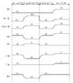
도 4는 상술한 도 3의 프로그램 동작시에 인가되는 전압들을 시간의 흐름에 따라 도시한 파형도이다. 도 4의 파형도에는 본 발명의 제 1 검증 동작을 포함하는 프로그램 동작시 인가되는 전압들이 시간의 순서에 따라 예시적으로 도시되었다.4 is a waveform diagram illustrating voltages applied in the above-described program operation of FIG. 3 over time. In the waveform diagram of FIG. 4, voltages applied during a program operation including the first verify operation of the present invention are exemplarily shown in order of time.
고전압 셋업 구간(T1) 동안, 전압 레귤레이터(140)에 의해서 고전압들이 설정된다. 뒤따라, 프로그램 실행 구간(T2) 동안, 전압 레귤레이터(140)로부터 제공되는 고전압들이 선택 라인들, 워드 라인들 및 벌크에 제공된다. 특히 벌크 영역으로는 음의 고전압(VBLK=-6V)이, 선택 워드 라인(Sel.WL)으로는 프로그램 전압(Vpgm= 10V)이 제공된다. 비트 라인들에는 프로그램 데이터에 대응하는 비트 라인 전압들이 제공된다. 데이터 '0'에 대응하는 비트 라('0' BL)인으로는 음의 고전압(-6V)이, 데이터 '1'에 대응하는 비트 라인('1' BL)으로는 프로그램 금지를 위한 0V가 제공된다.During the high voltage setup period T1, high voltages are set by the
프로그램 실행 구간(T2)이 종료되면, 벌크 영역에 바이어스된 음의 고전압을 접지 레벨로 방전하기 위한 방전 구간(T3)이 뒤따른다. 벌크 영역에 대응하는 등가 용량(Equivalent Capacitance)은 상대적으로 크기 때문에 음전하(Negative charge)를 방전하기 위한 방전 시간도 상대적으로 길다. 따라서, 벌크 영역이 0V의 전압으로 셋업될 때까지는 지연 시간이 소요된다. 이러한 지연 시간은 프로그램 속도를 저하시키는 요인으로 작용한다.When the program execution section T2 ends, a discharge section T3 for discharging the negative high voltage biased to the bulk region to ground level follows. Since the equivalent capacitance corresponding to the bulk region is relatively large, the discharge time for discharging the negative charge is also relatively long. Therefore, it takes a delay time until the bulk region is set up to a voltage of 0V. This delay is a factor that slows down the program.
방전 구간(T3)이 종료되면, 메모리 셀은 벌크 영역으로는 0V, 선택 워드 라인으로는 2V, 비선택 워드 라인들로는 5V, 그리고 비트 라인들로는 1V가 인가됨으로써 검증 동작이 수행된다(T4). 벌크 영역에 충전된 음전하들의 방전에 따라, 메모리 셀의 문턱전압은 바디 효과(Body effect)의 영향을 받지 않는다. 바디 효과(Body effect)로부터 자유로운 조건에서, 메모리 셀들 간의 문턱전압 특성은 획일화될 수 있다. 따라서, 효과적인 검증 동작이 가능하여 문턱전압 산포(Threshold distribution)가 조밀하게 제어될 수 있다.When the discharge period T3 ends, the verification operation is performed by applying 0 V as the bulk region, 2 V as the selected word line, 5 V as the unselected word lines, and 1 V as the bit lines (T4). According to the discharge of the negative charges charged in the bulk region, the threshold voltage of the memory cell is not affected by the body effect. In a condition free from the body effect, the threshold voltage characteristic between the memory cells may be uniform. Thus, an effective verification operation is possible so that the threshold voltage distribution can be tightly controlled.
상술한 벌크 영역의 음전하들이 방전되어야 하는 제 1 검증 동작은 방전에 필요한 시간만큼 프로그램 속도는 감소된다. 또한, 프로그램 루프를 반복적으로 수행해야 하는 경우, 음의 고전압의 충전과 방전을 반복적으로 수행해야 한다. 따라서, 제 1 검증 동작을 포함하는 프로그램 동작에서 프로그램 속도의 저하는 필연적이다.In the first verification operation in which the negative charges in the bulk region described above are to be discharged, the program speed is reduced by the time required for discharging. In addition, when the program loop must be repeatedly performed, the negative high voltage charge and discharge must be repeatedly performed. Therefore, a decrease in program speed is inevitable in a program operation including the first verify operation.
도 5는 본 발명의 제 2 실시예에 따른 프로그램 방법을 간략히 보여주는 순서도이다. 도 5를 참조하면, 본 발명의 제 2 실시예에 따른 프로그램 방법은 벌크 영역의 방전 동작을 수행하지 않고도 메모리 셀의 프로그램 여부를 검증하는 제 2 검증 동작을 포함한다. 좀더 자세히 설명하면 다음과 같다.5 is a flowchart schematically showing a program method according to a second embodiment of the present invention. Referring to FIG. 5, the program method according to the second exemplary embodiment of the present invention includes a second verifying operation of verifying whether a memory cell is programmed without performing a discharge operation of a bulk region. In more detail,
프로그램 동작이 시작되면, 프로그램 제어부(130)는 고전압 발생기(50)로부터 제공되는 고전압(High voltage)을 벌크(bulk)와 메모리 셀들의 워드 라인 및 선택 라인들로 분배하기 위한 셋업(High voltage setup) 동작을 수행한다. 프로그램 제어부(130)는 벌크로 제공되는 음의 고전압(-6V)을 전달하도록 전압 레귤레이터(140)를 제어한다. 프로그램 제어부(130)는 선택 라인들(SSL, GSL) 및 워드 라인들로 프로그램 전압(Vpgm)과 패스 전압(Vpass)을 제공하도록 전압 레귤레이터(140)를 제어한다. 예를 들면 상술한 표 1에 기재된 프로그램 실행시에 제공되는 제반 전압들이 활성화되도록 프로그램 제어부(130)는 전압 레귤레이터(140) 및 행 디코더(110)를 제어한다(S100). 고전압의 셋업 동작이 완료되면, 프로그램 제어부(130)는 고전압들을 벌크(bulk), 선택 라인들(SSL, GSL), 워드 라인들로 공급하여 프로그램을 실행한다. 프로그램 실행 동작시, 벌크 영역과 선택 워드 라인 사이에는 약 16V 의 전위차가 존재한다. 약 16V의 전위차에 의하여 데이터 '0'를 프로그램하는 메모리 셀의 플로팅 게이트로는 F-N 터널링을 유발할 수 있는 크기의 전계가 형성된다. 반면에, 데이터 '1'이 프로그램되는 메모리 셀의 비트 라인은 0V가 인가됨으로써 프로그램 금지(Program inhibit)로 설정된다(S110). 프로그램을 위한 전압 펄스(예를 들면 ISPP)의 인가가 종료되면, 프로그램의 패스 여부를 판단하기 위한 검증 동작이 뒤따른다. 그러나 본 발명의 제 2 검증 동작(2nd verify operation)에 따르면, 벌크 영역은 음의 고전압을 유지한 채, 검증 전압들이 제반 단자들로 제공된다. 제 2 검증 동작시, 벌크 영역은 음의 고전압으로 바이어스된 상태이기 때문에 제 1 검증 동작에 비해 상대적으로 낮은 워드 라인 전압으로 패스 여부의 판정이 가능하다. 하지만, 이때 워드 라인으로 제공되는 검증 전압들은 음의 고전압으로 충전된 벌크 영역에 의해서 발생하는 바디 효과(Body effect)가 고려되어야 한다. 따라서, 이러한 바디 효과를 고려하여 메모리 셀의 증가된 문턱전압을 보상할 수 있도록 워드 라인 전압은 벌크 영역에 인가된 음의 고전압이 고려된 전압으로부터 소폭 증가된 값으로 제공되어야 한다. 즉, 제 2 검증 동작시 선택 워드 라인으로는 0V, 비선택 워드 라인들로는 3V가 인가된다. 이러한 제 2 검증 동작시의 워드 라인 전압은 벌크 영역의 전위가 -6V이기 때문에 야기되는 바디 효과를 보상하기 위한 전압 레벨들이다(S120). 이상의 검증 동작에 따라 페이지 버퍼(120)에 래치되는 데이터를 참조하여 프로그램 제어부(130)는 프로그램 동작의 패스 또는 페일 여부를 판단한다(S130). 선택된 메모리 셀들 중 프로그램 페일(Fail)로 판별된 셀들이 존재하면, 절차는 재프로그램을 위한 단계 (S100)으로 궤환한다. 그러나, 선택된 메모리 셀들이 모두 프로그램 패스(Program pass)로 판정되면, 프로그램 동작은 종료된다. 여기서, 프로그램 동작을 위해 벌크 영역에 충전된 음의 고전압을 유지한 채 검증 동작을 수행하는 단계들(S120~S130)은 제 2 검증 동작을 구성한다.When the program operation is started, the
상술한 제 2 검증 동작을 포함하는 낸드 플래시 메모리의 프로그램 동작에 따르면, 벌크 영역의 음의 고전압을 유지한 채로 검증 동작이 수행된다. 따라서, 바디 효과(Body effect)에 따르는 메모리 셀의 문턱전압의 변화를 고려해야 한다. 반면에, 벌크 영역에 충전된 음의 전하들을 방전하기 위한 동작을 수행할 필요가 없기 때문에 본 발명의 제 2 실시예는 프로그램 속도를 증가시킬 수 있다.According to the program operation of the NAND flash memory including the second verify operation described above, the verify operation is performed while maintaining the negative high voltage of the bulk region. Therefore, the change in the threshold voltage of the memory cell due to the body effect should be considered. On the other hand, the second embodiment of the present invention can increase the program speed because it is not necessary to perform an operation for discharging the negative charges charged in the bulk region.
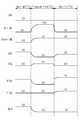
도 6은 상술한 도 5의 프로그램 동작시 각 구성들로 인가되는 전압들을 시간의 흐름에 따라 도시한 파형도이다. 도 6을 참조하면, 본 발명의 벌크 영역의 방전 동작없이 프로그램 검증을 수행하기 위한 바이어스 조건이 각 단계별로 도시되었다.FIG. 6 is a waveform diagram illustrating voltages applied to respective components in the program operation of FIG. 5 as time passes. Referring to FIG. 6, a bias condition for performing program verification without discharging a bulk region of the present invention is illustrated for each step.
고전압 셋업 구간(T1) 및 프로그램 실행 구간(T2) 동안, 전압 레귤레이터(140)에 의해서 제공되는 고전압들은 도 4의 고전압 셋업 구간(T1) 및 프로그램 실행 구간(T2)과 동일하다. 그러나, 프로그램 실행 구간(T2) 이후에 이루어지는 제 2 검증 구간(T4)은 제 1 검증 동작과 달리 벌크 영역의 방전없이 이루어진다. 즉, 벌크 영역에 음의 고전압(-6V)을 유지한 채 워드 라인 및 비트 라인들로 검증 전압들이 제공된다. 이때 워드 라인으로 제공되는 검증 전압들은 벌크 영역에 제공되는 음의 고전압에 의해서 야기되는 바디 효과(Body effect)를 고려한 전압들이다. 바디 효과(Body effect)는 메모리 셀의 벌크 바이어스에 따른 문턱전압 변화를 의미한다. 벌크 바이어스 상태에 따라, 메모리 셀의 채널에서의 자유 전하 밀도(Free charge density)는 변동하게 된다. 채널에서의 자유 전하 밀도에 따라 메모리 셀의 문턱전압은 변한다. 아래 수학식 1은 벌크 전압의 변동에 따른 문턱전압(Vth)의 변화를 나타내는 바디 효과를 간략히 설명하고 있다.During the high voltage setup period T1 and the program execution period T2, the high voltages provided by the

예시적으로, 선택 워드 라인으로는 0V, 비선택 워드 라인들로는 3V의 전압이 인가된다. For example, a voltage of 0 V is selected as the selected word line and 3 V is applied to the unselected word lines.
상술한 바와 같이 제 2 검증 동작을 포함하는 프로그램 동작은 벌크 영역에 충전된 음전하들을 방전할 필요가 없다. 프로그램 루프를 반복할 경우에도 충방전을 위한 시간 소모를 최소화할 수 있다. 따라서, 제 2 검증 동작을 채택하는 플래시 메모리 장치는 프로그램 속도를 증가시킬 수 있다.As described above, the program operation including the second verify operation does not need to discharge the negative charges charged in the bulk region. Even when the program loop is repeated, time for charging and discharging can be minimized. Thus, the flash memory device adopting the second verify operation can increase the program speed.
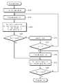
도 7은 상술한 제 1 검증 동작과 제 2 검증 동작을 프로그램 루프 수에 따라 선택적으로 수행하는 본 발명의 제 3 실시예를 간략히 보여주는 순서도이다. 도 7을 참조하면, 특정 프로그램 루프 수(k) 이하의 프로그램 구간에서는 벌크의 방전 없이 검증 동작이 이루어지는 제 2 검증 동작에 따르는 프로그램 동작을 수행한다. 이후에 특정 프로그램 루프 수(k)에 도달하게 되면, 벌크를 방전한 뒤에 검증 동작을 수행하는 제 1 검증 동작을 수행하도록 설정된다. 좀더 자세히 설명하면 다음과 같다.7 is a flowchart schematically illustrating a third embodiment of the present invention for selectively performing the above-described first verify operation and second verify operation according to the number of program loops. Referring to FIG. 7, a program operation according to a second verify operation in which a verify operation is performed without discharge of a bulk is performed in a program section less than or equal to a specific program loop number k. Subsequently, when the specific program loop number k is reached, the first verify operation is performed to discharge the bulk and then perform the verify operation. In more detail,
프로그램 동작이 시작되면, 프로그램 제어부(130)는 벌크와 워드 라인들로 제공할 고전압들을 셋업한다(S200). 이어서 프로그램 실행(Program execution)을 위한 제반 동작들을 수행한다. 즉, 설정된 고전압들을 이용하여 벌크 영역으로는 -6V를 인가하도록 프로그램 제어부(130)는 전압 레귤레이터(140)를 제어한다. 마찬가지로 프로그램 제어부(130)는 셀 어레이(100)의 선택 워드 라인으로는 10V, 비선택 워드 라인들로는 3V가 인가되도록 행 디코더(110)를 제어한다(S210). 이후에는 벌크 영역에 인가된 음의 고전압이 유지된 상태에서 프로그램의 패스 여부를 검증하는 제 2 검증 동작이 수행된다(S220). 제 2 검증 동작에 의하여 선택된 모든 메모리 셀들이 패스(Pass)로 판정되면, 절차는 제 1 검증 동작을 위한 단계(S270)로 이동한다. 그러나, 제 2 검증 동작 결과 페일(Fail)로 판정되면, 현재의 프로그램 루프 수(x)를 카운트한다(S240). 현재의 루프 수(x)가 특정 루프 수(k)보다 작으면, 절차는 재프로그램을 위한 단계(S210)로 궤환한다. 그러나, 현재의 루프 수(x)가 특정 루프 수(k) 이상인 경우, 절차는 제 1 검증 동작에 의해서 패스 여부가 검증되도록 단계(S260)로 이동한다. 이어서, 선택된 메모리 셀들은 벌크 영역이 음의 고전압으로 충전된 상태에서 프로그램된다(S260). 그리고, 벌크 영역이 0V로 방전된 이후에 검증 동작이 수행되는 제 1 검증 동작이 수행된다(S270). 제 1 검증 동작의 결과가 페일(fail)로 판정되면, 절차는 재프로그램을 위한 단계 (S260)으로 이동한다. 제 1 검증 동작의 결과가 패스(Pass)로 판정되면, 제반 프로그램 동작은 종료된다.When the program operation is started, the
상술한 본 발명의 제 3 실시예에 따른 프로그램 방법은, 특정 루프 수에 미치기 이전까지의 프로그램 동작시에는 제 2 검증 동작에 따라서 메모리 셀들을 검증한다. 그리고 프로그램 루프 수가 특정 루프 수 이상에 도달하면, 제 1 검증 동작에 따라 메모리 셀들을 검증한다. 제 2 검증 동작만을 프로그램 동작에 적용하는 경우, 메모리 셀들에 발생하는 바디 효과(body effect)가 동일하지 않기 때문이다. 바디 효과에 따른 문턱전압의 상승이 메모리 셀들마다 동일하지 않을 경우, 메모리 셀들의 문턱전압 산포는 확장되고 읽기 마진은 감소된다. 그러나, 바디 효과가 차단되는 제 1 검증 동작을 프로그램 사이클 내에서 후반 루프들에 적용하면, 문턱전압의 산포를 조밀하게 설정할 수 있다. 따라서, 특정 루프 수(k) 미만에서 진행되는 제 2 검증 동작은 프로그램 속도를 증가시킬 수 있고, 특정 루프 수(k) 이상에서 진행되는 제 1 검증 동작은 문턱전압 산포를 개선할 수 있다. 결국, 본 발명의 제 3 실시예는 프로그램 속도의 증가와 문턱전압 산포의 개선을 모두 구현할 수 있다.The program method according to the third embodiment of the present invention described above verifies memory cells according to a second verify operation during a program operation until reaching a specific number of loops. When the number of program loops reaches more than a certain number of loops, the memory cells are verified according to the first verify operation. When only the second verify operation is applied to the program operation, the body effects occurring in the memory cells are not the same. If the increase in the threshold voltage due to the body effect is not the same for each memory cell, the threshold voltage distribution of the memory cells is expanded and the read margin is reduced. However, applying the first verify operation in which the body effect is blocked to the latter loops within the program cycle allows for a tight distribution of the threshold voltage. Accordingly, the second verify operation performed below the specific loop number k may increase the program speed, and the first verify operation performed above the specific loop number k may improve the threshold voltage distribution. As a result, the third embodiment of the present invention can implement both an increase in program speed and an improvement in threshold voltage distribution.
도 8은 제 1 검증 동작과 제 2 검증 동작을 페일된 비트 수에 따라서 선택적으로 수행하는 본 발명의 제 4 실시예를 간략히 보여주는 순서도이다. 도 8을 참조하면, 프로그램 페일로 검출된 비트 수(Y)가 특정 비트 수(Z) 미만인 프로그램 구간에서는 벌크의 방전 없이 검증 동작이 이루어지는 제 2 검증 동작에 따라 프로그램 동작을 수행한다. 이후에 페일로 판정된 메모리 셀들의 수(Y)가 특정 비트 수(Z) 미만에 도달하게 되면, 벌크의 음전하들이 방전된 뒤에 검증 동작을 수행하는 제 1 검증 동작을 수행하도록 단계들이 설정된다. 좀더 자세히 설명하면 다음과 같다.8 is a flowchart briefly illustrating a fourth embodiment of the present invention for selectively performing a first verify operation and a second verify operation according to the number of failed bits. Referring to FIG. 8, a program operation is performed according to a second verify operation in which a verify operation is performed without bulk discharge in a program section in which the number of bits Y detected as a program fail is less than a specific number of bits Z. Subsequently, when the number Y of memory cells determined to fail reaches less than a specific number of bits Z, the steps are set to perform a first verify operation that performs a verify operation after the discharge of the negative negative charges. In more detail,
프로그램 동작이 시작되면, 프로그램 제어부(130)는 벌크와 워드 라인들로 제공할 고전압들을 셋업한다(S300). 이어서 프로그램 제어부(130)는 프로그램 실행(Program execution)을 위한 제반 제어 동작들을 수행한다. 즉, 프로그램 제어부(130)는 설정된 고전압들을 이용하여 벌크 영역으로는 -6V를 인가하도록 전압 레귤레이터(140)를 제어한다. 마찬가지로 프로그램 제어부(130)는 셀 어레이(100)의 선택 워드 라인으로는 10V, 비선택 워드 라인들로는 3V가 인가되도록 행 디코더(110)를 제어한다(S310). 이후에는 벌크 영역에 인가된 음의 고전압이 유지된 상태에서 프로그램에 따른 메모리 셀의 패스 여부를 검증하는 제 2 검증 동작이 수행된다(S320). 제 2 검증 동작에 따라, 선택된 모든 메모리 셀들이 패스(Pass)로 판정되면, 절차는 벌크 영역을 방전한 상태에서 프로그램의 패스 여부를 재검증하기 위한 제 1 검증 동작을 위한 단계(S370)로 이동한다. 그러나, 제 2 검증 동작 결과 페일(fail)로 판정되면, 현재의 절차에서 검출된 페일 비트(fail bit)의 수(Y)를 카운트한다(S340). 비트 스캐닝을 통해서 검출된 페일 비트(fail bit)의 수(Y)가 특정 비트 수(Z)보다 크면, 절차는 재프로그램을 위한 단계 (S310)으로 궤환한다. 그러나, 현재의 프로그램 루프 내에서 검출된 페일 비트 수(Y)가 특정 비트 수(Z) 미만인 경우, 제 1 검증 동작에 의거하여 페일(fail)로 판정된 셀들이 프로그램되도록 절차는 단계(S360)로 이동한다(S350). 제 1 검증 동작에 의거하여 페일(fail) 로 판정된 셀들은 그 벌크 영역으로는 음의 고전압이 제공되는 동시에 워드 라인과 비트 라인들로 프로그램을 위한 전압들이 인가된다(S360). 그리고, 프로그램 제어부(130)는 벌크 영역이 0V로 방전된 이후에 검증 동작이 수행되는 제 1 검증 동작이 수행한다(S370). 제 1 검증 동작의 결과가 페일로 판정되면, 절차는 재프로그램을 위한 단계 (S360)으로 이동한다. 제 1 검증 동작의 결과가 패스(Pass)로 판정되면, 제반 프로그램 동작은 종료된다.When the program operation starts, the
이상에서 설명된 본 발명의 제 4 실시예는 제 2 검증 동작 및 제 1 검증 동작이 모두 프로그램 절차에 포함된다. 본 발명의 제 4 실시예에 따르면, 벌크 영역의 방전이 없이 검증 동작이 수행되는 제 2 검증 동작을 적용하여 프로그램 속도를 높일 수 있다. 그리고 벌크 영역을 방전한 이후에 검증 동작을 수행하는 제 1 검증 동작을 프로그램 동작의 후반부에 적용하여 조밀한 문턱전압 산포를 갖도록 메모리 셀들을 제어할 수 있다. 따라서, 본 발명의 제 4 실시예의 프로그램 방법을 적용하는 낸드 플래시 메모리 장치는 프로그램 속도의 향상과 셀들의 문턱전압 산포를 개선할 수 있다.In the fourth embodiment of the present invention described above, both the second verify operation and the first verify operation are included in the program procedure. According to the fourth embodiment of the present invention, the program speed may be increased by applying the second verify operation in which the verify operation is performed without discharge of the bulk region. The memory cells may be controlled to have a dense threshold voltage distribution by applying a first verification operation that performs a verification operation after discharging the bulk region to the second half of the program operation. Therefore, the NAND flash memory device applying the program method of the fourth embodiment of the present invention can improve the program speed and the threshold voltage distribution of the cells.
이상의 설명에 따른 본 발명의 낸드 플래시 메모리는 노어형 플래시 메모리와 공유할 수 있는 고전압 조건에서 프로그램 동작을 수행하는 임베디드 낸드 플래시 메모리를 예시적으로 개시하였다. 그러나, 본 발명은 임베디드 낸드 플래시 메모리에만 국한되지는 않는다. 본 발명의 프로그램 방법이 사용될 수 있는 모든 반도체 메모리 장치들에 대해서 적용될 수 있음은 이 분야에서 통상의 지식을 습득한 자들에게 자명하다.The NAND flash memory of the present invention according to the above description has exemplarily disclosed an embedded NAND flash memory for performing a program operation under a high voltage condition that can be shared with a NOR flash memory. However, the present invention is not limited to embedded NAND flash memory. It is apparent to those skilled in the art that the program method of the present invention can be applied to all semiconductor memory devices that can be used.
이상에서와 같이 도면과 명세서에서 최적 실시예가 개시되었다. 여기서 특정한 용어들이 사용되었으나, 이는 단지 본 발명을 설명하기 위한 목적에서 사용된 것이지 의미 한정이나 특허청구범위에 기재된 본 발명의 범위를 제한하기 위하여 사용된 것은 아니다. 그러므로 본 기술 분야의 통상의 지식을 가진 자라면 이로부터 다양한 변형 및 균등한 타 실시예가 가능하다는 점을 이해할 것이다. 따라서, 본 발명의 진정한 기술적 보호 범위는 첨부된 특허청구범위의 기술적 사상에 의해 정해져야 할 것이다.As described above, optimal embodiments have been disclosed in the drawings and the specification. Although specific terms have been used herein, they are used only for the purpose of describing the present invention and are not used to limit the scope of the present invention as defined in the meaning or claims. Therefore, those skilled in the art will understand that various modifications and equivalent other embodiments are possible from this. Therefore, the true technical protection scope of the present invention will be defined by the technical spirit of the appended claims.
이상과 같은 본 발명에 의하면, 벌크 영역에 음의 고전압을 반복적으로 방전 또는 충전할 필요가 없기 때문에 고속으로 프로그램 가능한 낸드 플래시 메모리 장치를 구현할 수 있다. 그리고, 본 발명은 고속의 프로그램 속도와 조밀한 문턱전압 산포를 제공할 수 있어 고속 및 신뢰성 높은 메모리 장치를 제공할 수 있다.According to the present invention as described above, since it is not necessary to discharge or charge negative high voltage repeatedly in the bulk region, a NAND flash memory device that can be programmed at high speed can be implemented. In addition, the present invention can provide a high program speed and a compact threshold voltage distribution, thereby providing a high speed and reliable memory device.
Claims (45)
Translated fromKoreanPriority Applications (2)
| Application Number | Priority Date | Filing Date | Title |
|---|---|---|---|
| KR1020070008024AKR100850516B1 (en) | 2007-01-25 | 2007-01-25 | Flash memory device and program method thereof |
| US11/769,429US7672170B2 (en) | 2007-01-25 | 2007-06-27 | Flash memory device and program method thereof |
Applications Claiming Priority (1)
| Application Number | Priority Date | Filing Date | Title |
|---|---|---|---|
| KR1020070008024AKR100850516B1 (en) | 2007-01-25 | 2007-01-25 | Flash memory device and program method thereof |
Publications (2)
| Publication Number | Publication Date |
|---|---|
| KR20080070245A KR20080070245A (en) | 2008-07-30 |
| KR100850516B1true KR100850516B1 (en) | 2008-08-05 |
Family
ID=39669248
Family Applications (1)
| Application Number | Title | Priority Date | Filing Date |
|---|---|---|---|
| KR1020070008024AExpired - Fee RelatedKR100850516B1 (en) | 2007-01-25 | 2007-01-25 | Flash memory device and program method thereof |
Country Status (2)
| Country | Link |
|---|---|
| US (1) | US7672170B2 (en) |
| KR (1) | KR100850516B1 (en) |
Cited By (2)
| Publication number | Priority date | Publication date | Assignee | Title |
|---|---|---|---|---|
| KR101036300B1 (en)* | 2009-04-30 | 2011-05-23 | 주식회사 하이닉스반도체 | Flash memory device and program method thereof |
| US9570176B2 (en) | 2014-10-22 | 2017-02-14 | Samsung Electronics Co., Ltd. | Nonvolatile memory device, storage device having the same, operating method thereof |
Families Citing this family (20)
| Publication number | Priority date | Publication date | Assignee | Title |
|---|---|---|---|---|
| KR100927119B1 (en)* | 2007-05-10 | 2009-11-18 | 삼성전자주식회사 | Nonvolatile Semiconductor Memory Device And Its Programming Method |
| US7760551B2 (en)* | 2007-09-11 | 2010-07-20 | Samsung Electronics Co., Ltd. | Method of programming nonvolatile memory device |
| KR101430169B1 (en) | 2007-09-11 | 2014-08-14 | 삼성전자주식회사 | Programming method of non-volatile memory device |
| KR100933858B1 (en)* | 2007-11-13 | 2009-12-24 | 주식회사 하이닉스반도체 | Nonvolatile Memory Devices and Their Bulk Voltage Control Methods |
| KR100936879B1 (en)* | 2007-12-28 | 2010-01-14 | 주식회사 하이닉스반도체 | Erasing Method and Soft Programming Method of Nonvolatile Memory Device |
| US7990772B2 (en)* | 2009-03-11 | 2011-08-02 | Micron Technology Inc. | Memory device having improved programming operation |
| US20110149667A1 (en)* | 2009-12-23 | 2011-06-23 | Fatih Hamzaoglu | Reduced area memory array by using sense amplifier as write driver |
| KR101721005B1 (en)* | 2010-01-22 | 2017-03-29 | 삼성전자주식회사 | Method of programming a non-volatile semiconductor memory device |
| KR20110093257A (en)* | 2010-02-12 | 2011-08-18 | 삼성전자주식회사 | Nonvolatile Memory Device and Its Operation Method |
| US8295095B2 (en) | 2010-04-20 | 2012-10-23 | Micron Technology, Inc. | Programming methods for a memory device |
| KR101131945B1 (en)* | 2010-07-07 | 2012-03-29 | 주식회사 하이닉스반도체 | Non-volatile memory device |
| US9007832B2 (en)* | 2011-03-03 | 2015-04-14 | Micron Technology, Inc. | Methods for programming a memory device and memory devices |
| KR101678919B1 (en) | 2011-05-02 | 2016-11-24 | 삼성전자주식회사 | Memory system and error correction method |
| KR101874408B1 (en)* | 2011-11-09 | 2018-07-05 | 삼성전자주식회사 | Nonvolatile memory device and memory system including the same |
| JP5911834B2 (en)* | 2013-09-11 | 2016-04-27 | 株式会社東芝 | Nonvolatile semiconductor memory device |
| US20160189786A1 (en)* | 2014-12-24 | 2016-06-30 | Sandisk Technologies Inc. | Methods and apparatus for reducing read time for nonvolatile memory devices |
| US9703494B1 (en)* | 2016-09-26 | 2017-07-11 | Intel Corporation | Method and apparatus for protecting lower page data during programming in NAND flash |
| WO2018076239A1 (en)* | 2016-10-27 | 2018-05-03 | Micron Technology, Inc. | Erasing memory cells |
| JP6832375B2 (en)* | 2019-02-25 | 2021-02-24 | ウィンボンド エレクトロニクス コーポレーション | How to Protect Semiconductor Integrated Circuits from Reverse Engineering |
| KR20240110432A (en)* | 2023-01-06 | 2024-07-15 | 삼성전자주식회사 | Non-volatile memory device and operating method thereof |
Citations (5)
| Publication number | Priority date | Publication date | Assignee | Title |
|---|---|---|---|---|
| US6943402B2 (en) | 2003-05-30 | 2005-09-13 | Kabushiki Kaisha Toshiba | Nonvolatile semiconductor memory device including MOS transistors each having a floating gate and control gate |
| US6961268B2 (en) | 2003-08-28 | 2005-11-01 | Kabushiki Kaisha Toshiba | Nonvolatile semiconductor memory device with MOS transistors each having a floating gate and a control gate |
| US7122866B2 (en) | 2004-03-19 | 2006-10-17 | Kabushiki Kaisha Toshiba | Semiconductor memory device with a stacked gate including a floating gate and a control gate and method of manufacturing the same |
| US7136306B2 (en) | 2002-10-07 | 2006-11-14 | Interuniversitair Microelektronica Centrum (Imec) | Single bit nonvolatile memory cell and methods for programming and erasing thereof |
| US7280407B2 (en) | 2004-04-23 | 2007-10-09 | Kabushiki Kaisha Toshiba | Semiconductor memory device including floating gates and control gates, control method for the same, and memory card including the same |
Family Cites Families (6)
| Publication number | Priority date | Publication date | Assignee | Title |
|---|---|---|---|---|
| KR970051375A (en) | 1995-12-29 | 1997-07-29 | 김주용 | Flash memory device |
| JPH10223866A (en)* | 1997-02-03 | 1998-08-21 | Toshiba Corp | Semiconductor storage device |
| US6304486B1 (en) | 1999-12-20 | 2001-10-16 | Fujitsu Limited | Sensing time control device and method |
| KR20030001611A (en) | 2001-06-25 | 2003-01-08 | 주식회사 하이닉스반도체 | Flash memory device and method of programing using the same |
| KR100618902B1 (en)* | 2005-06-17 | 2006-09-01 | 삼성전자주식회사 | Program method of flash memory device that can shorten program time by thermal scan during program verification read |
| US7525838B2 (en)* | 2006-08-30 | 2009-04-28 | Samsung Electronics Co., Ltd. | Flash memory device and method for programming multi-level cells in the same |
- 2007
- 2007-01-25KRKR1020070008024Apatent/KR100850516B1/ennot_activeExpired - Fee Related
- 2007-06-27USUS11/769,429patent/US7672170B2/ennot_activeExpired - Fee Related
Patent Citations (5)
| Publication number | Priority date | Publication date | Assignee | Title |
|---|---|---|---|---|
| US7136306B2 (en) | 2002-10-07 | 2006-11-14 | Interuniversitair Microelektronica Centrum (Imec) | Single bit nonvolatile memory cell and methods for programming and erasing thereof |
| US6943402B2 (en) | 2003-05-30 | 2005-09-13 | Kabushiki Kaisha Toshiba | Nonvolatile semiconductor memory device including MOS transistors each having a floating gate and control gate |
| US6961268B2 (en) | 2003-08-28 | 2005-11-01 | Kabushiki Kaisha Toshiba | Nonvolatile semiconductor memory device with MOS transistors each having a floating gate and a control gate |
| US7122866B2 (en) | 2004-03-19 | 2006-10-17 | Kabushiki Kaisha Toshiba | Semiconductor memory device with a stacked gate including a floating gate and a control gate and method of manufacturing the same |
| US7280407B2 (en) | 2004-04-23 | 2007-10-09 | Kabushiki Kaisha Toshiba | Semiconductor memory device including floating gates and control gates, control method for the same, and memory card including the same |
Cited By (2)
| Publication number | Priority date | Publication date | Assignee | Title |
|---|---|---|---|---|
| KR101036300B1 (en)* | 2009-04-30 | 2011-05-23 | 주식회사 하이닉스반도체 | Flash memory device and program method thereof |
| US9570176B2 (en) | 2014-10-22 | 2017-02-14 | Samsung Electronics Co., Ltd. | Nonvolatile memory device, storage device having the same, operating method thereof |
Also Published As
| Publication number | Publication date |
|---|---|
| US7672170B2 (en) | 2010-03-02 |
| US20080183951A1 (en) | 2008-07-31 |
| KR20080070245A (en) | 2008-07-30 |
Similar Documents
| Publication | Publication Date | Title |
|---|---|---|
| KR100850516B1 (en) | Flash memory device and program method thereof | |
| US9343154B2 (en) | Nonvolatile memory device and driving method thereof | |
| US7796444B2 (en) | Concurrent programming of non-volatile memory | |
| US8873297B2 (en) | Select gate programming in a memory device | |
| KR101407361B1 (en) | Non-volatile memory device and program method thereof | |
| KR100502412B1 (en) | Non-volatile semiconductor memory device and program method thereof | |
| US9953704B2 (en) | Semiconductor memory device | |
| KR101358752B1 (en) | Nonvolatile memory device, memory system having its, and programming method thereof | |
| CN103081015B (en) | Programming nonvolatile memory using stepwise increases in bit line voltage | |
| KR101463584B1 (en) | Nonvolatile memory device and its programming method | |
| US8174891B2 (en) | Non-volatile semiconductor memory device and method of writing data in non-volatile semiconductor memory devices | |
| US20050207229A1 (en) | Nonvolatile semiconductor memory | |
| US8638606B2 (en) | Substrate bias during program of non-volatile storage | |
| JP2008140488A (en) | Semiconductor memory device | |
| JP5198524B2 (en) | Nonvolatile semiconductor memory | |
| WO2020214217A1 (en) | Memory device with channel discharge before program-verify based on data state and sub-block position | |
| WO2021021251A1 (en) | Maintaining channel pre-charge in program operation | |
| WO2014136295A1 (en) | Nonvolatile semiconductor memory device and read method thereof | |
| US20110292734A1 (en) | Method of programming nonvolatile memory device | |
| KR102416047B1 (en) | Method for controlling dummy cell and semiconduntor device | |
| US8953371B2 (en) | Semiconductor storage device | |
| US20120140572A1 (en) | Semiconductor memory device and method of operating the same | |
| US8559227B2 (en) | Nonvolatile memory device | |
| KR100927119B1 (en) | Nonvolatile Semiconductor Memory Device And Its Programming Method |
Legal Events
| Date | Code | Title | Description |
|---|---|---|---|
| A201 | Request for examination | ||
| PA0109 | Patent application | St.27 status event code:A-0-1-A10-A12-nap-PA0109 | |
| PA0201 | Request for examination | St.27 status event code:A-1-2-D10-D11-exm-PA0201 | |
| E902 | Notification of reason for refusal | ||
| PE0902 | Notice of grounds for rejection | St.27 status event code:A-1-2-D10-D21-exm-PE0902 | |
| E13-X000 | Pre-grant limitation requested | St.27 status event code:A-2-3-E10-E13-lim-X000 | |
| P11-X000 | Amendment of application requested | St.27 status event code:A-2-2-P10-P11-nap-X000 | |
| P13-X000 | Application amended | St.27 status event code:A-2-2-P10-P13-nap-X000 | |
| E701 | Decision to grant or registration of patent right | ||
| PE0701 | Decision of registration | St.27 status event code:A-1-2-D10-D22-exm-PE0701 | |
| GRNT | Written decision to grant | ||
| PG1501 | Laying open of application | St.27 status event code:A-1-1-Q10-Q12-nap-PG1501 | |
| PR0701 | Registration of establishment | St.27 status event code:A-2-4-F10-F11-exm-PR0701 | |
| PR1002 | Payment of registration fee | St.27 status event code:A-2-2-U10-U11-oth-PR1002 Fee payment year number:1 | |
| PG1601 | Publication of registration | St.27 status event code:A-4-4-Q10-Q13-nap-PG1601 | |
| PR1001 | Payment of annual fee | St.27 status event code:A-4-4-U10-U11-oth-PR1001 Fee payment year number:4 | |
| R18-X000 | Changes to party contact information recorded | St.27 status event code:A-5-5-R10-R18-oth-X000 | |
| FPAY | Annual fee payment | Payment date:20120706 Year of fee payment:5 | |
| PR1001 | Payment of annual fee | St.27 status event code:A-4-4-U10-U11-oth-PR1001 Fee payment year number:5 | |
| FPAY | Annual fee payment | Payment date:20130701 Year of fee payment:6 | |
| PR1001 | Payment of annual fee | St.27 status event code:A-4-4-U10-U11-oth-PR1001 Fee payment year number:6 | |
| LAPS | Lapse due to unpaid annual fee | ||
| PC1903 | Unpaid annual fee | St.27 status event code:A-4-4-U10-U13-oth-PC1903 Not in force date:20140731 Payment event data comment text:Termination Category : DEFAULT_OF_REGISTRATION_FEE | |
| PC1903 | Unpaid annual fee | St.27 status event code:N-4-6-H10-H13-oth-PC1903 Ip right cessation event data comment text:Termination Category : DEFAULT_OF_REGISTRATION_FEE Not in force date:20140731 |