KR100849572B1 - Planarization of substrates using electrochemical mechanical polishing - Google Patents
Planarization of substrates using electrochemical mechanical polishingDownload PDFInfo
- Publication number
- KR100849572B1 KR100849572B1KR1020037009383AKR20037009383AKR100849572B1KR 100849572 B1KR100849572 B1KR 100849572B1KR 1020037009383 AKR1020037009383 AKR 1020037009383AKR 20037009383 AKR20037009383 AKR 20037009383AKR 100849572 B1KR100849572 B1KR 100849572B1
- Authority
- KR
- South Korea
- Prior art keywords
- substrate
- electrolyte
- substrate surface
- polishing
- delete delete
- Prior art date
- Legal status (The legal status is an assumption and is not a legal conclusion. Google has not performed a legal analysis and makes no representation as to the accuracy of the status listed.)
- Expired - Fee Related
Links
Images


Classifications
- H—ELECTRICITY
- H01—ELECTRIC ELEMENTS
- H01L—SEMICONDUCTOR DEVICES NOT COVERED BY CLASS H10
- H01L21/00—Processes or apparatus adapted for the manufacture or treatment of semiconductor or solid state devices or of parts thereof
- H01L21/02—Manufacture or treatment of semiconductor devices or of parts thereof
- H01L21/04—Manufacture or treatment of semiconductor devices or of parts thereof the devices having potential barriers, e.g. a PN junction, depletion layer or carrier concentration layer
- H01L21/18—Manufacture or treatment of semiconductor devices or of parts thereof the devices having potential barriers, e.g. a PN junction, depletion layer or carrier concentration layer the devices having semiconductor bodies comprising elements of Group IV of the Periodic Table or AIIIBV compounds with or without impurities, e.g. doping materials
- H01L21/30—Treatment of semiconductor bodies using processes or apparatus not provided for in groups H01L21/20 - H01L21/26
- H01L21/302—Treatment of semiconductor bodies using processes or apparatus not provided for in groups H01L21/20 - H01L21/26 to change their surface-physical characteristics or shape, e.g. etching, polishing, cutting
- H01L21/304—Mechanical treatment, e.g. grinding, polishing, cutting
- B—PERFORMING OPERATIONS; TRANSPORTING
- B23—MACHINE TOOLS; METAL-WORKING NOT OTHERWISE PROVIDED FOR
- B23H—WORKING OF METAL BY THE ACTION OF A HIGH CONCENTRATION OF ELECTRIC CURRENT ON A WORKPIECE USING AN ELECTRODE WHICH TAKES THE PLACE OF A TOOL; SUCH WORKING COMBINED WITH OTHER FORMS OF WORKING OF METAL
- B23H5/00—Combined machining
- B23H5/06—Electrochemical machining combined with mechanical working, e.g. grinding or honing
- B23H5/08—Electrolytic grinding
Landscapes
- Engineering & Computer Science (AREA)
- Chemical & Material Sciences (AREA)
- Chemical Kinetics & Catalysis (AREA)
- Electrochemistry (AREA)
- Mechanical Engineering (AREA)
- Manufacturing & Machinery (AREA)
- Condensed Matter Physics & Semiconductors (AREA)
- General Physics & Mathematics (AREA)
- Physics & Mathematics (AREA)
- Computer Hardware Design (AREA)
- Microelectronics & Electronic Packaging (AREA)
- Power Engineering (AREA)
- Mechanical Treatment Of Semiconductor (AREA)
- Finish Polishing, Edge Sharpening, And Grinding By Specific Grinding Devices (AREA)
- Formation Of Insulating Films (AREA)
- Weting (AREA)
Abstract
Translated fromKoreanDescription
Translated fromKorean본 출원은 2001년 3월 14일자로 제출된 미국 가특허출원 시리얼 넘버 60/275,874, 2001년 4월 24일자로 제출된 미국 가특허출원 시리얼 넘버 60/286,107 및 2001년 10월 1일자로 제출된 미국 가특허출원 시리얼 넘버 60/326,263의 장점을 청구하는 것으로서, 각각이 참조로서 여기에 포함될 수 있다.This application is filed on U.S. Provisional Serial No. 60 / 275,874, filed Mar. 14, 2001, U.S. Provisional Serial No. 60 / 286,107, filed April 24, 2001, and on 1 October 2001. Claiming the advantages of US Provisional Patent Application Serial No. 60 / 326,263, each of which may be incorporated herein by reference.
본 발명은 기판 위에 금속과 같은 물질의 평탄화(planarization)를 위한 장치 및 방법에 관한 것이다.The present invention relates to an apparatus and method for planarization of materials such as metals on a substrate.
서브-쿼터(sub-quarter) 마이크론 다층 금속 배선은 차세대 초고밀도 집적(ULSI)의 핵심기술 중 하나이다. 이 기술의 핵심인 다층 배선은 접점, 비아(via), 라인 및 다른 피처(feature)들을 포함하는, 높은 종횡비(high aspect ratio) 애퍼쳐(aperture)에서 형성되는 배선 피처들의 평탄화를 필요로 한다. 이러한 배선 피처들의 신뢰할 수 있는 형태는 ULSI의 성공에 매우 중요하고, 각각의 기판과 다이(die)의 회로 밀도 및 품질을 향상시키기 위한 지속적인 노력에도 매우 중요하다.Sub-quarter micron multilayer metallization is one of the key technologies in the next generation of ultra high density integration (ULSI). Multilayer interconnects, the heart of this technology, require planarization of interconnect features formed at high aspect ratio apertures, including contacts, vias, lines, and other features. The reliable form of these wiring features is critical to ULSI's success, and is also critical to ongoing efforts to improve the circuit density and quality of each substrate and die.
집적회로 및 다른 전자 장치의 제조에 있어서, 도체, 반도체 및 유전체 물질의 다중층들은 기판 표면에 증착되거나 기판 표면에서 제거된다. 많은 증착 기술을 통해 도체, 반도체 및 유전체 물질의 박막층이 증착될 수 있다. 현대적인 프로세싱에서 일반적인 증착기술은 스퍼터링(sputtering)으로 알려진 물리적 기상증착(PVD), 화학적 기상증착(CVD), 플라즈마 강화 화학적 기상증착(PECVD) 및 현재의 전기화학적 도금(ECP)을 포함한다.In the manufacture of integrated circuits and other electronic devices, multiple layers of conductors, semiconductors, and dielectric materials are deposited on or removed from the substrate surface. Many deposition techniques allow the deposition of thin layers of conductor, semiconductor, and dielectric materials. Common deposition techniques in modern processing include physical vapor deposition (PVD), chemical vapor deposition (CVD), plasma enhanced chemical vapor deposition (PECVD), and current electrochemical plating (ECP), known as sputtering.
물질층들이 순차적으로 증착되고 제거됨에 따라, 기판의 최상부 표면은 그 표면 전체에 대해 비-평면이 될 수 있고 평탄화를 필요로 한다. 표면을 평탄하게 하는 것 또는 기판을 "연마(polishing)"하는 것은 일반적으로 평탄한 평면을 형성하기 위해 물질이 기판 표면에서 제거되는 공정이다. 평탄화는 거친 표면, 응결 물질, 결정 래티스 손상, 스크래치 및 오염된 층 또는 물질과 같은 바람직하지 않은 표면 토포그래피와 표면 결함을 제거하는데 사용된다. 또한, 평탄화는 피처들을 채우고 순차적 단계의 금속배선 및 프로세싱을 위해 평평한 표면을 제공하는데 사용되는 물질의 과도한 증착을 제거함으로써, 기판에 피처들을 형성하는데 유용하다.As the layers of material are deposited and removed sequentially, the top surface of the substrate may be non-planar with respect to the entire surface and require planarization. Leveling the surface or “polishing” the substrate is generally a process by which material is removed from the substrate surface to form a flat plane. Planarization is used to remove undesirable surface topography and surface defects such as rough surfaces, condensation materials, crystal lattice damage, scratches and contaminated layers or materials. In addition, planarization is useful for forming features in the substrate by filling the features and eliminating excessive deposition of materials used to provide a flat surface for subsequent metallization and processing.
화학 기계적 평탄화, 또는 화학 기계적 연마(CMP)는 기판 평탄화에 사용되는 통상의 기술이다. CMP는 기판으로부터 물질을 선택적으로 제거하기 위해 화학적 합성물, 통상 슬러리(slurry) 또는 다른 유체 매질을 사용한다. 종래의 CMP 기술에서, 기판 캐리어 또는 연마 헤드는 캐리어 조립장치(assembly)에 결합하고, CMP 장치의 연마 패드와 접촉하는 곳에 위치한다. 상기 캐리어 조립장치는 기판에 제어가능한 압력을 제공하여 연마 패드에 대해 기판을 가압한다. 상기 패드는 외부의 구동력에 의해 기판에 대해 이동된다. CMP 장치는 상기 기판 표면과 연마 패드 사이에서 연마 또는 마찰 운동을 일으키고, 연마 화합물 또는 슬러리를 분산함으로써, 화학적 및/또는 기계적으로 활성 작용하여, 결과적으로 기판의 표면에서 물질을 제거한다.Chemical mechanical planarization, or chemical mechanical polishing (CMP), is a common technique used for substrate planarization. CMP uses chemical compounds, usually slurries or other fluid media, to selectively remove material from the substrate. In conventional CMP technology, the substrate carrier or polishing head is coupled to the carrier assembly and positioned in contact with the polishing pad of the CMP apparatus. The carrier assembly provides controllable pressure to the substrate to press the substrate against the polishing pad. The pad is moved relative to the substrate by an external driving force. The CMP apparatus produces a polishing or frictional motion between the substrate surface and the polishing pad and disperses the polishing compound or slurry, thereby acting chemically and / or mechanically, thereby removing material from the surface of the substrate.
구리는 집적회로 및 다른 전자 장치에서 전도성 경로를 제공하는 배선을 형성하기 위해 ULSI에서 채택되는 금속이 되고 있다. 구리는 알루미늄과 같은 기존 물질과 비교해 볼 때, 낮은 저항 및 더 좋은 전자 이동성과 같은 바람직한 특성을 갖는 물질이다. 구리는 PVD, CVD 및 전기도금(electroplating)과 같은 다양한 기술들을 통해 증착될 수 있다. 전기도금(ECP)은 저비용이고 유망한 효율적인 증착 기술이다. ECP는 기판을 도금 배스(plating bath)에 삽입하고, 기판에 전류를 인가함으로써 수행된다. 구리 이온들은 용액으로부터 석출되어 기판에 증착된다.Copper is becoming the metal adopted by ULSI to form interconnects that provide conductive paths in integrated circuits and other electronic devices. Copper is a material with desirable properties such as lower resistance and better electron mobility compared to conventional materials such as aluminum. Copper can be deposited through various techniques, such as PVD, CVD, and electroplating. Electroplating (ECP) is a low cost and promising efficient deposition technique. ECP is performed by inserting a substrate into a plating bath and applying a current to the substrate. Copper ions are deposited from the solution and deposited on the substrate.
그러나 구리는 패턴화 및 에칭하기가 어렵다. 따라서, 구리 피처들은 다마신(damascene) 또는 듀얼 다마신 공정을 이용하여 형성해야 한다. 다마신 공정에서, 피처는 유전체 물질에 형성되고 순차적으로 구리로 채워진다. 베리어층은 구리의 증착 전에 유전체 층에 형성된 상기 피처들의 표면상에 일치되게 증착된다. 그리고 상기 베리어층과 주변 필드 위에 구리가 증착된다. 유전체 물질에 구리로 충전된 피처를 형성되도록 하기 위해, 필드 위에 증착된 구리는 CMP 공정에 의해 제거된다. 연마재(abrasive) CMP 공정 및 무 연마재 CMP 공정 모두 이용될 수 있고, 구리를 제거하기 위한 다른 방법들이 개발되고 있다. 연마재는 연마 슬러리에 첨가되거나 연마시 고정-연마재 연마 패드로부터 방출되는, 알루미나 또는 실리카와 같은, 입자 물질을 나타내고, 연마되는 기판 표면에 기계적 마모를 제공한다.However, copper is difficult to pattern and etch. Therefore, copper features must be formed using a damascene or dual damascene process. In the damascene process, the features are formed in the dielectric material and sequentially filled with copper. The barrier layer is deposited consistently on the surface of the features formed in the dielectric layer prior to the deposition of copper. Copper is then deposited on the barrier layer and the surrounding field. In order to form copper-filled features in the dielectric material, copper deposited over the field is removed by a CMP process. Both abrasive CMP processes and abrasive free CMP processes can be used, and other methods for removing copper are being developed. The abrasive represents a particulate material, such as alumina or silica, added to the polishing slurry or released from the fixed-abrasive polishing pad upon polishing, and provides mechanical wear to the substrate surface to be polished.
또한, 기판 표면은 형성된 피처들의 밀도 또는 크기에 따라 서로 다른 표면 토포그래피를 가질 수 있고, 기판 표면으로부터 구리 물질을 효과적이고 일치하게 제거하기 어렵게 한다. 예를 들어, 구리 물질은, 형성된 피처들이 거의 없는 기판 표면에서 구리 물질을 제거하는 것과 비교할 때, 기판 표면의 조밀 피처 영역에서 더 느린 제거 속도로 제거되는 것이 관측되었다. 또한, 비교적 일정하지 않은 제거 속도는 연마 공정 이후에 남는 잔여 구리 물질을 갖는 기판 영역에 과소 연마(under polishing)를 초래할 수 있다.In addition, the substrate surface may have different surface topography depending on the density or size of the features formed, making it difficult to effectively and consistently remove copper material from the substrate surface. For example, it has been observed that copper material is removed at a slower removal rate in the dense feature areas of the substrate surface as compared to removing copper material from the substrate surface with few features formed. In addition, relatively inconsistent removal rates can result in under polishing in areas of the substrate with residual copper material remaining after the polishing process.
기판 표면으로부터 모든 원하는 구리 물질을 제거하기 위한 하나의 해결 방법은 기판 표면을 과도 연마(over polishing)하는 것이다. 그러나 몇 가지 물질에서의 과도 연마는, 디싱(dishing)이라고 칭하는 피처의 함몰이나, 침식(erosion)이라고 칭하는 유전체 물질의 과도한 제거와 같은 토포그래피 결함의 형성을 야기할 수 있다. 디싱 및 침식과 같은 토포그래피 결함들은, 그 아래에 증착된 베리어층의 물질과 같은 부가 물질을 불균일하게 제거할 수도 있고, 요구되는 연마 품질보다 낮은 연마 품질을 갖는 기판 표면을 형성할 수도 있다.One solution for removing all desired copper material from the substrate surface is to over polish the substrate surface. However, overpolishing in some materials can lead to the formation of topographical defects, such as the depression of features called dishing or excessive removal of dielectric material called erosion. Topographical defects such as dishing and erosion may unevenly remove additional materials, such as the material of the barrier layer deposited thereon, and may form a substrate surface having a polishing quality lower than the polishing quality required.
구리 표면 연마의 다른 문제점은 기판 표면에서 구리 다마신을 형성하기 위해 낮은 유전 상수(k)를 갖는 유전 물질을 사용함으로써 발생한다. 탄소로 도프된 실리콘 산화막(carbon doped silicon oxide)과 같은 낮은 k의 유전 물질은, 종래의 연마 압력(즉, 약 6psi)에서 변형되거나 스크래치 날 수 있고(다운포스(downforce)라 함), 기판 연마 품질과 장치 형태에 결정적인 영향을 끼칠 수 있다. 예를 들어, 기판과 연마 패드 사이의 상대적 회전 운동은 기판 표면을 따라 전단력(shear force)을 유도하고 낮은 k의 물질을 변형시켜서 스크래치와 같은 토포그래피 결함을 형성할 수 있으며, 이것은 이후의 연마에 결정적인 영향을 끼칠 수 있다.Another problem with copper surface polishing arises from using dielectric materials with low dielectric constants (k) to form copper damascene at the substrate surface. Low k dielectric materials, such as carbon doped silicon oxide, can deform or scratch at conventional polishing pressures (ie, about 6 psi) (called downforce), and substrate polishing It can have a decisive impact on quality and device type. For example, the relative rotational motion between the substrate and the polishing pad can induce shear forces along the substrate surface and deform the low k material to form topographical defects such as scratches, which can be used for subsequent polishing. It can have a decisive impact.
따라서, 기판에 구리층과 같은 금속층을 증착하고 평탄화하기 위한 장치 및 방법이 필요하다.Accordingly, what is needed is an apparatus and method for depositing and planarizing a metal layer, such as a copper layer, on a substrate.
본 발명의 목적은 기판과 연마 장치 사이의 감소된 접촉 압력으로 기판 표면을 평탄화하는 방법 및 장치를 제공하는 것이다. 일 실시예에 따른, 기판의 처리 방법은, 부식 억제제(corrosion inhibitor)를 포함하는 전해액에 기판을 위치시키는 단계, 기판 표면상에 패시베이션층(passivation layer)을 형성하는 단계, 상기 전해액에서 상기 기판을 연마하는 단계, 상기 기판 표면에 애노드 바이어스(anodic bias)를 인가하는 단계 및 적어도 상기 기판 표면의 일부분으로부터 물질을 제거하는 단계를 포함한다.It is an object of the present invention to provide a method and apparatus for planarizing a substrate surface with a reduced contact pressure between the substrate and the polishing apparatus. According to an embodiment, a method of treating a substrate may include: placing a substrate in an electrolyte including a corrosion inhibitor, forming a passivation layer on a surface of the substrate, and removing the substrate from the electrolyte. Polishing, applying an anode bias to the substrate surface and removing material from at least a portion of the substrate surface.
다른 실시예에 따른 기판의 처리 방법은, 기판 표면에 전류 억제층(current suppressing layer)을 형성하기 위해, 연마 제품과 인접하게 전해액-전해액은 부식 억제제, 균염제(leveling agent), 점착 형성제(viscous forming agent) 또는 이들의 조합을 포함한다-에 기판을 위치시키는 단계, 적어도 상기 전류 억제층의 일부분을 제거하기 위해, 상기 연마 제품으로 상기 전해액의 기판을 연마하는 단계, 상기 전해액에 배치된 애노드와 캐소드 사이에 바이어스를 인가하는 단계 및 애노드 용해(anodic dissolution)로 적어도 상기 기판 표면의 일부분에서 물질을 제거하는 단계를 포함한다.According to another embodiment of the present invention, a method of treating a substrate may include: an electrolyte-electrolyte is used as a corrosion inhibitor, a leveling agent, and a adhesion agent to form a current suppressing layer on the surface of the substrate. forming a substrate, and polishing the substrate of the electrolyte with the abrasive product to remove at least a portion of the current suppression layer, an anode disposed in the electrolyte, Applying a bias between the cathodes and removing material from at least a portion of the substrate surface with an anode dissolution.
다른 실시예에서, 기판의 처리 장치는, 처리 영역을 형성하고 유체 입구(fluid inlet)와 유체 출구(fluid outlet)를 갖는 부분 외장(partial enclosure), 상기 부분 외장에 배치되는 캐소드, 상기 부분 외장에 배치되는 연마 제품, 상기 연마 제품상에 이동 가능하게 배치되고 기판 장착 표면을 갖는 기판 캐리어, 적어도 상기 부분 외장과 연결되는 전원, 및 상기 장치로 하여금 기판을 전해액에 위치시켜서 기판 표면상에 패시베이션층을 형성하고, 상기 연마 제품으로 상기 전해액에서 기판을 연마시키며, 상기 기판 표면 또는 연마 제품에 애노드 바이어스를 인가하여 적어도 상기 기판 표면의 일부분에서 물질을 제거시키도록 구성되는 컴퓨터 기반의 컨트롤러를 포함한다.In another embodiment, a processing apparatus for a substrate includes a partial enclosure defining a processing region and having a fluid inlet and a fluid outlet, a cathode disposed on the partial enclosure, and a partial enclosure. An abrasive product to be disposed, a substrate carrier movably disposed on the abrasive product, the power supply being connected to at least the partial sheath, and the device positioning the substrate in the electrolyte to provide a passivation layer on the substrate surface. A computer-based controller configured to form, polish the substrate in the electrolyte with the abrasive article, and apply an anode bias to the substrate surface or abrasive article to remove material from at least a portion of the substrate surface.
다른 실시예에서, 전기화학적 증착 시스템이 제공되며, 상기 시스템은 메인프레임 웨이퍼 전달 로봇을 갖는 메인프레임, 상기 메인프레임에 연결 배치되는 로딩 스테이션, 상기 메인프레임과 연결 배치되는 하나 이상의 전기화학적 프로세싱 셀, 상기 메인프레임과 연결 배치되는 하나 이상의 연마판(polishing platen), 상기 하나 이상의 전기화학적 프로세싱 셀에 유동적으로 연결되는 전해액 공급기 및 상기 하나 이상의 전기화학적 프로세싱 셀에 연결된 하나 이상의 연마액 공급기를 포함한다.In another embodiment, an electrochemical deposition system is provided, the system comprising a mainframe having a mainframe wafer transfer robot, a loading station disposed in connection with the mainframe, one or more electrochemical processing cells disposed in connection with the mainframe, And at least one polishing platen disposed in connection with the mainframe, an electrolyte supply fluidly connected to the at least one electrochemical processing cell, and at least one polishing liquid supply connected to the at least one electrochemical processing cell.
위에서 설명한 특징들을 여기서 기술하는, 방식이 잘 전달되고 상세히 이해될 수 있게 하기 위해서, 위에서 요약한 본 발명의 보다 구체적인 설명을, 첨부한 도면에 나타난 실시예들을 참조로 할 것이다.BRIEF DESCRIPTION OF THE DRAWINGS In order that the features described above may be well conveyed and understood in detail, the foregoing detailed description of the invention will be made with reference to the embodiments shown in the accompanying drawings.
그러나 첨부된 도면들은 단지 본 발명의 전형적인 실시예들을 나타내는 것이며, 본 발명은 다른 동등한 효과적인 실시예들을 허용할 수 있으므로, 본 발명의 범위를 제한하는 것으로 생각해서는 안 된다는 점을 주의해야 한다.It should be noted, however, that the appended drawings illustrate only typical embodiments of the invention and that they should not be construed as limiting the scope of the invention, as the invention may permit other equivalent effective embodiments.
도 1은 본 발명의 처리 장치의 실시예들을 포함하는 처리 시스템의 일 실시예의 평면도이다.1 is a plan view of one embodiment of a processing system including embodiments of the processing apparatus of the present invention.
도 2는 전기도금 시스템의 일 실시예의 개념적 상면도이다.2 is a conceptual top view of one embodiment of an electroplating system.
도 3은 전기도금 시스템의 다른 실시예의 개념적 상면도이다.3 is a conceptual top view of another embodiment of an electroplating system.
도 4는 투과 디스크 위에 위치한 기판을 도시하는 본 발명의 처리 장치의 일 실시예의 횡단면도이다.4 is a cross-sectional view of one embodiment of a processing apparatus of the present invention showing a substrate positioned over a transmission disk.
도 5는 캐리어 헤드 조립장치의 일 실시예를 나타내는 부분 횡단면도이다.5 is a partial cross-sectional view showing one embodiment of a carrier head assembly.
도 6a는 다수의 기판 클램프의 부분 사시도이다.6A is a partial perspective view of a plurality of substrate clamps.
도 6b는 도 6a의 라인 6B-6B를 따라 절개한 상기 기판 클램프들 중 하나의 횡단면도이다.FIG. 6B is a cross-sectional view of one of the substrate clamps taken along
도 7a 내지 도 7d는 상기 캐리어 헤드 조립장치에 고정되는 기판을 나타낸다.7a to 7d show a substrate fixed to the carrier head assembly.
도 8은 캐리어 헤드 조립장치의 다른 실시예를 나타내는 부분도이다.8 is a partial view showing another embodiment of the carrier head assembly.
도 9는 캐리어 헤드 조립장치의 다른 실시예를 나타내는 부분도이다.9 is a partial view showing another embodiment of the carrier head assembly.
도 10a 및 도 10b는 캐리어 헤드 조립장치 실시예들의 부분도이다.10A and 10B are partial views of carrier head assembly embodiments.
도 11a 내지 도 11d는 기판상에 금속층을 증착하고 평탄화하기 위한 장치의 실시예들의 개념적 횡단면도이다.11A-11D are conceptual cross sectional views of embodiments of an apparatus for depositing and planarizing a metal layer on a substrate.
도 12는 본 발명의 일 실시예에 따른 처리 단계들을 나타내는 흐름도이다.12 is a flowchart showing processing steps according to an embodiment of the present invention.
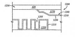
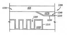
도 13a 내지 도 13f는 여기서 언급되는 기판 표면을 평탄화하기 위한 일 실시예에 따른 기판 연마의 개념도이다.13A-13F are conceptual diagrams of substrate polishing according to one embodiment for planarizing the substrate surface referred to herein.
일반적으로 본 발명의 실시예들은 기판과 연마 장치 사이에 감소된 접촉 압력으로 기판 표면을 평탄화하기 위한 장치 및 방법을 제공한다. 본 발명은 전기화학 기계적 연마(ECMP) 기술을 이용해, 구리 및 기타 구리를 포함하는 물질들과 같은, 전도성 물질들을 기판 표면에서 제거하기 위한 평탄화 공정을 이하에서 참조로 설명할 것이다.In general, embodiments of the present invention provide an apparatus and method for planarizing a substrate surface with reduced contact pressure between the substrate and the polishing apparatus. The present invention will be described below with reference to a planarization process for removing conductive materials from a substrate surface, such as copper and other copper-containing materials, using electrochemical mechanical polishing (ECMP) techniques.
여기서 사용되는 단어 및 용어들은, 추가로 더 정의되지 않는 한, 본 기술분야의 당업자에게 본 기술분야에서 사용되는 통상적인 관례적 의미로 주어진다. 화학적-기계적 연마는 화학적 활동, 기계적 활동 또는 화학적 및 기계적 활동의 조합에 의해 기판 표면을 침식시키는 것을 포함하는 것이나, 이것만으로 제한하지 않고 폭넓게 구성될 수 있다. 전기연마(electropolishing)는 애노드 용해와 같은 전기화학적 활동의 응용예에 의해 기판에서 물질을 제거하는 것을 포함하는 것이나, 이것만으로 제한하지 않고 폭넓게 구성될 수 있다. 애노드 용해는, 기판 표면 또는 상기 기판 표면에 붙어있는 전도성 물체에 애노드 바이어스를 인가하여, 기판 표면에서 주변 전도성 유체로 전동성 물질을 이동하게 하는 것으로서, 여기서 폭넓게 언급된다. 전기화학적 기계적 연마(ECMP)는 전기화학적 활동, 화학적 활동, 기계적 활동 또는 그들의 조합의 응용예에 의해 기판을 평탄화하여 기판 표면에서 물질을 제거하는 것으로서 여기서 폭넓게 정의될 수 있다. 여기서 언급되는 공정들을 수행하는데 사용되는 예시적인 처리 시스템은 도 1 내지 도 3에서 나타낸다.The words and terms used herein, unless further defined, are given to those of ordinary skill in the art in the conventional customary meaning used in the art. Chemical-mechanical polishing includes, but is not limited to, eroding the substrate surface by chemical activity, mechanical activity, or a combination of chemical and mechanical activity, and can be broadly configured. Electropolishing includes removing material from a substrate by application of electrochemical activity, such as anode dissolution, but can be widely configured without limitation. Anode dissolution is broadly referred to herein as the application of an anode bias to a substrate surface or a conductive object affixed to the substrate surface, thereby causing the motorized material to move from the substrate surface to the surrounding conductive fluid. Electrochemical mechanical polishing (ECMP) can be broadly defined herein as the removal of material from the substrate surface by planarizing the substrate by application of electrochemical activity, chemical activity, mechanical activity or a combination thereof. Exemplary processing systems used to perform the processes referred to herein are shown in FIGS.
도 1은 여기서 언급된 공정들을 수행하기 위한 처리 시스템(100)의 일 실시예를 나타낸다. 본 발명으로부터 이득을 얻기 위해, 채택할 수 있는 하나의 연마 툴로는 캘리포니아 산타 클레라에 위치한 어플라이드 머티어리얼스 사의 Mirra® Mesa™ 화학적 기계적 연마기가 있다. 예시되는 시스템(100)은 팩토리 인터페이스(108), 로딩 로봇(110), 및 그 위에 위치하는 적어도 하나의 전기화학적 처리 스테이션(102)과 적어도 하나의 종래의 연마 스테이션(106)을 갖는 처리 모듈(112)을 포함한다.1 illustrates one embodiment of a
일반적으로, 로딩 로봇(110)은 팩토리 인터페이스(108)와 처리 모듈(112)에 인접하게 배치되어 이들 간에 기판(122)의 전달을 용이하게 한다. 팩토리 인터페이스(108)는 일반적으로 클리닝 모듈(114)과 하나 이상의 기판 카세트(116)를 포함한다. 인터페이스 로봇(118)은 기판 카세트(116), 클리닝 모듈(114) 및 입력 모듈(120) 간에 기판(123)을 전달하기 위해 사용된다. 입력 모듈(120)은, 로딩 로봇(110)에 의한 처리 모듈(112)과 팩토리 인터페이스(108) 간의 기판(123) 전달을 용이하게 하도록 위치한다. 유리하게 사용될 수 있는 팩토리 인터페이스의 일 예는, 2000년 4월 11일자로 제출되고 공동 출원인 어플라이드 머티어리얼스 사에게 양도된 미국 특허출원번호 09/547,189에 공개되어 있고, 참조로 본 발명에 포함될 수 있다.In general, the
로딩 로봇(110)은 일반적으로 팩토리 인터페이스(108)와 처리 모듈(112)에 근접하여 위치하고, 로봇(110)에 의해 제공되는 동작 범위가 이들 간의 기판(123) 전달을 용이하게 한다. 로딩 로봇(110)의 일 예로는 캘리포니아 리치몬드에 위치한 켄싱턴 레버토리즈(Kensington Laboratories) 사에 의해 제조된 4링크 로봇이 있다. 예시되는 로딩 로봇(110)은 수직 또는 수평 방향으로 기판(123)을 향하게 하는 그립퍼(gripper: 111)를 갖는다.The
도 1에서 도시하는 일 실시예에서, 예시되는 처리 모듈(112)은 전달 스테이션(122), 캐루젤(carousel:134), 전기화학적 처리 스테이션(102) 및 연마 스테이션(106)을 갖고, 이들은 모두 기계 베이스(126)에 배치된다. 처리 모듈(112)은 하나 이상의 처리 스테이션을 포함할 수 있고, 모듈(112)의 각각의 스테이션(102, 106)은, 전기증착과 전기연마와 같은 전기화학적 처리를 수행하고, 종래의 화학적 연마 처리, 종래의 기계적 연마 처리 또는 이들을 조합한 처리를 수행하도록 적용될 수 있다. 각 연마 스테이션(106)은 고정 연마판, 회전 연마판, 선형 연마판, 회전 선형 연마판, 롤러 연마판, 혹은 이들의 조합을 포함할 수 있다. 연마 스테이션(106)에 배치되는 연마 제품은, 전도성이 있을 수 있고, 및/또는 연마재 소자 또는 입자를 포함할 수 있다.In one embodiment shown in FIG. 1, the illustrated
일 실시예에서, 전달 스테이션(122)은 적어도 입력버퍼 스테이션(128), 출력버퍼 스테이션(130), 전달 로봇(132) 및 로드 컵 조립장치(124)를 포함한다. 전달 로봇(132)은 두 개의 그립퍼 조립장치들을 갖고, 각각은 기판 테두리로 기판(123)을 쥐는 압축공기식 그립퍼 핑거(pneumatic gripper finger)를 갖는다. 전달 로봇(132)은 입력버퍼 스테이션(128)에서 기판(123)을 들어올리고, 상기 그립퍼 및 기판(123)을 회전시켜서 기판(123)을 로드 컵 조립장치(124) 상에 위치시킨 후, 기판(123)을 로드 컵 조립장치(124) 아래로 놓는다. 유리하게 사용할 수 있는 전달 스테이션의 일 예는, 1999년 10월 10일자로 제출되고 공동 출원인 어플라이드 머티어리얼스 사로 양도된 미국 특허출원번호 09/314,771에서 Tobin에 의해 공개되었으며, 참조로 본 발명에 포함될 수 있다.In one embodiment, the
캐루젤(134)은 일반적으로 1998년 9월 8일자로 Tolles 등이 출원한 미국특허 제 5,804,507 호에 언급되어 있으며, 그 전체가 참조로 본 발명에 포함될 수 있다. 일반적으로, 캐루젤(134)은 베이스(126)의 중심에 배치된다. 캐루젤(134)은 통상 다수의 암(136)을 포함한다. 각각의 암은 캐리어 헤드 조립장치 또는 연마 헤드(138)를 지지한다. 도 1에 도시된 암(136)들 중 하나는 가상으로 나타냈으므로 전달 스테이션(122)을 나타낼 수 있다. 캐루젤(134)은 인덱서블(indexable)하므로 연마 헤드(138)는 모듈(102, 106)과 전달 스테이션(122) 사이에서 이동될 수 있다.
일반적으로 연마 헤드(138)는 연마 스테이션(106)에 배치된 연마 물질(미도시)에 대하여 상기 기판을 가압할 때 기판(123)을 지탱한다. 이용될 수 있는 하나의 연마 헤드로는 캘리포니아 산타 클레라의 어플라이드 머티어리얼스 사에 의해 제조된 Titan HeadTM 기판 캐리어가 있다.Generally, the polishing
또한, 도시되지는 않았지만, 기판 표면의 기계적 연마, 기판으로부터의 전기화학적 물질 제거, 또는 시스템(100)에서의 기판 전달과 같이, 시스템상 하나 이상의 처리 단계들을 시스템(100)이 수행하도록 명령하기 위한 컴퓨터 시스템 또는 컴퓨터 기반의 컨트롤러 혹은 컴퓨터 프로그램 제품이 시스템(100)과 연결될 수 있다. 선택적으로, 전기화학적 증착 또는 동시작용(concurrent) 전기화학적 증착 및 전기연마가 수행된다면, 상기 컴퓨터 시스템, 컴퓨터 기반의 컨트롤러 또는 컴퓨터 프로그램 제품도 상기한 단계들을 수행하도록 채택될 수 있다.Also, although not shown, for instructing the
상기에서 언급된 바와 같은 시스템(100)의 제어를 용이하게 하기 위한 컴퓨터 기반의 컨트롤러(140)는, 다양한 챔버와 서브프로세서들을 제어하기 위한 산업 설비에 사용될 수 있는, CPU(144) 또는 다른 형태의 컴퓨터 프로세서 중 하나일 수 있다. 메모리(142)는 CPU(144)와 결합하고, 상기 메모리 혹은 컴퓨터가 읽을 수 있는 매체는, 랜덤 액세스 메모리(RAM), 롬(ROM), 플로피 디스크, 하드 디스크 또는 다른 형태의 디지털 저장장치와 같은, 로컬이든 원격이든, 하나 이상의 읽기 가능한 메모리일 수 있다. 지원 회로(146)는 종래의 방식으로 프로세서를 지원하기 위해 CPU(144)에 결합된다. 이러한 회로들은 캐시, 전력 공급기, 클록회로, 입출력 회로 및 서브시스템 등을 포함한다. 본 발명에서 언급되는 공정들의 애스팩트(aspect)에 의한 것과 같이 처리 시퀀스는, 통상적인 소프트웨어 루틴으로, 일반적으로 상기 메모리에 저장된다. 또한, 소프트웨어 루틴은 CPU(144)에 의해 제어되는 하드웨어로부터 떨어진 곳에 위치하는 제 2 CPU(미도시)를 통해 저장 및/또는 실행될 수도 있다.Computer-based
도 2는 본 발명에서 설명되는 공정들을 수행하기 위한, 적어도 하나의 전기화학적 처리 스테이션(218)과 적어도 하나의 종래의 연마 스테이션(215)을 갖는 처리 시스템(200)의 다른 실시예를 도시하는 개념적 상면도이다. 본 발명에서 장점으로 채택될 수 있는 하나의 툴로는 캘리포니아 산타 클레라에 위치한 어플라이드 머티어리얼스 사의 Electra® 처리 시스템과 같은, 전기화학적 처리 플랫폼 또는 시스템이 있다.2 is a conceptual diagram illustrating another embodiment of a
시스템(200)은 로딩 스테이션(210)과 메인프레임(214)을 포함한다. 메인프레임(214)은 일반적으로 메인프레임 전달 스테이션(216), 스핀-린스 건조(SRD) 스테이션(212), 하나 이상의 전기화학적 처리 스테이션(218) 및 하나 이상의 연마 스 테이션(215)을 포함한다. 시스템(200)은 또한 급속 열적 어닐링(RTA) 챔버(211)와 같은 열적 어닐링 챔버, 전해액 보급 시스템(220) 및 하나 이상의 기판 관통 카세트(238)를 포함할 수 있다.
각각의 전기화학적 처리 스테이션(218)은 하나 이상의 전기화학적 프로세싱 셀(240)을 포함한다. 전해액 보급 시스템(220)은 메인프레임(214)과 인접하여 위치하고 프로세싱 셀(240)에 연결되어 개별적으로 전기도금 공정에 사용되는 전해액을 순환시킨다. 각각의 연마 스테이션(215)은 하나 이상의 연마판(217)을 포함한다. 연마판(217)은 고정 연마판, 회전 연마판, 선형 연마판, 회전 선형 연마판, 본 발명에서 언급되는 바와 같이 롤러를 포함하는 판 또는 셀, 또는 이들의 조합과 상기 판 위 또는 안에 위치한 연마 제품을 포함할 수 있다. 연마판(217)에 위치한 연마 제품은, 전도성이 있을 수 있고/있거나 연마재 소자 또는 입자를 포함할 수 있다.Each
또한, 시스템(200)은 시스템에 전력을 공급하기 위한 전력 공급기 스테이션(221)과 제어 시스템(222)을 포함한다. 전력 공급기 스테이션(221)은 각각 전기화학적 셀(240)과 연마판(217)에 연결되는 하나 이상의 전원을 포함한다. 제어 시스템(222)은, 시스템(200)의 모든 컴포넌트들을 제어하고 시스템(200)의 다양한 컴포넌트의 작동을 조정하기 위해 구체적으로 설계되는, 컴퓨터가 읽을 수 있는 매체, 즉 소프트웨어를 갖는 프로그래밍 가능한 마이크로프로세서를 포함한다. 제어 시스템(222)은 또한 상기 시스템의 컴포넌트들에 제공되는 전기 전력을 제어할 수 있다. 또한, 제어 시스템(222)은 운영자가 시스템(200)을 모니터하고 운영할 수 있게 하는 제어 패널을 포함할 수 있다. 상기 제어 패널은 케이블을 통해 제어 시스템(222)과 연결되어 운영자가 용이하게 접속할 수 있게 하는 독립 모듈이다.The
로딩 스테이션(210)은 하나 이상의 기판 카세트 수납 영역(224), 하나 이상의 로딩 스테이션 전달 로봇(228) 및 적어도 하나의 기판 방향자(substrate orientor: 230)를 포함하는 것이 바람직하다. 로딩 스테이션(210)에 포함되는 기판 카세트 수납 영역, 로딩 스테이션 전달 로봇(228) 및 기판 방향자의 개수는 상기 시스템의 원하는 작업량에 따라 조절될 수 있다. 도 2에서 나타낸 것처럼, 일 실시예의 로딩 스테이션(210)은 두 개의 기판 카세트 수납 영역(224), 두 개의 로딩 스테이션 전달 로봇(228) 및 하나의 기판 방향자(230)를 포함한다. 기판(234)을 포함하는 기판 카세트(232)는 기판 카세트 수납 영역(224)로 로딩되어 기판(234)을 시스템(200)으로 삽입시킨다. 로딩 스테이션 전달 로봇(228)은 기판 카세트(232)와 기판 방향자(230) 간에 기판(234)을 전달한다.The
기판 방향자(230)는 상기 기판이 적절히 처리되도록 보장하기 위해 원하는 방향으로 각각의 기판(234)을 위치시킨다. 또한, 로딩 스테이션 전달 로봇(228)은 로딩 스테이션(210)과 SRD 스테이션(212) 사이 및 로딩 스테이션(210)과 열적 어닐링 챔버(211) 사이에 기판(234)을 전달한다. 로딩 스테이션(210)은 또한 온 시스템 전체에 기판의 효율적인 전달을 용이하게 하는데 필요한, 기판들의 일시적인 보관을 위해 기판 카세트(231)를 포함하는 것이 바람직하다.
또한, 도 2는 상기 메인프레임 스테이션에 부착되는 서로 다른 스테이션 간에 기판을 전달하기 위해, 여기에 포함되는 플리퍼 로봇(flipper robot:244)을 갖는 메인프레임 전달 로봇(242)을 나타낸다. 메인프레임 전달 로봇(242)은 다수의 로봇 암(242, 두 개만 도시함)을 포함하며, 플리퍼 로봇(244)은 각각의 로봇 암(246)에 대한 엔드 이펙터(end effector)로서 부착되어, 메인프레임에 부착된 서로 다른 스테이션들간에 기판을 전달할 수 있고 원하는 표면 방향으로 상기 기판을 전달되도록 움직인다(flipping). 예를 들어, 플리퍼 로봇(244)은, 프로세싱 셀(240)에서의 전기화학적 공정 또는 연마판(217)에서의 연마 공정들을 위해 공정 중인 기판 표면이 아래를 향하도록(face-down) 움직이고, 스핀-린스-건조 공정 또는 기판 전달과 같은 다른 공정들을 위해 공정 중인 기판 표면이 위를 향하도록(face-up) 움직인다.2 also shows a
플리퍼 로봇은 통상 종래기술에 공지되어 있고, 캘리포니아 밀피타스에 위치한 로제 오토메이션(Rorze Automation) 사의 모델 RR701과 같은 기판 핸들링 로봇이 엔드 이펙터로서 부착될 수 있다. 또한, 플리퍼 로봇(244)은 플리퍼 위에 배치된 기판을 전기도금하기 위해 전기화학적 프로세싱 셀(240)과 함께 사용하기에 적합할 수 있고, 또는 전기화학적 프로세싱 셀(240)은 셀(240)에서의 처리 공정 전에 플리퍼 로봇으로부터 기판을 받기에 적합할 수 있다.Flipper robots are commonly known in the art, and substrate handling robots, such as Model RR701 from Rorze Automation, Milpitas, California, can be attached as end effectors. In addition, the
선택적으로 하나 이상의 전기화학적 처리 스테이션(218)과 하나 이상의 연마 스테이션(215), 이들 간에 기판을 전달하고, 및/또는 이 안의 기판들을 처리하기 위해서, 기판 캐리어(도 1에 도시된 것처럼)를 메인프레임 전달 로봇(242) 대신에 배치할 수 있다.Optionally, a substrate carrier (as shown in FIG. 1) may be used to transfer substrates between one or more
급속 열적 어닐링(RTA) 챔버(211)는 로딩 스테이션(210)에 연결되는 것이 바람직하고, 기판들은 로딩 스테이션 전달 로봇(228)에 의해 RTA 챔버(211) 내부 및 외부로 전달된다. 도 2에 도시된 바와 같은 상기 전기도금 시스템은, 일 실시예에서 로딩 스테이션(210)의 대칭 설계에 따라 로딩 스테이션(210)의 양 반대쪽에 배치되는 두 개의 RTA 챔버(211)를 포함한다. 적절한 어닐링 챔버의 일 예로는 캘리포니아 산타 클레라에 위치하는 어플라이드 머티어리얼스 사의 RTP XEplus Centura® 열적 프로세서와 같은, 급속 열적 어닐링 챔버가 있다.The rapid thermal annealing (RTA)
전해액 보급 시스템(220)은 전기도금 및/또는 애노드 용해 공정을 위해 전기도금 프로세싱 셀(240)에 전해액을 제공한다. 전해액 보급 시스템(220)은 일반적으로 메인 전해액 탱크(260), 다수의 소스 탱크(262) 및 다수의 필터 탱크(264)를 포함한다. 하나 이상의 컨트롤러는 메인 탱크(260) 안의 전해액 혼합과 전해액 보급 시스템(220)의 동작을 제어한다. 상기 컨트롤러들은 독립적으로 동작하지만, 시스템(200)의 제어 시스템(222)과 통합되는 것이 바람직하다.The
메인 전해액 탱크(260)는 전해액의 저장을 제공하고, 각각의 전기도금 프로세싱 셀에 연결되는 전해액 공급라인을 포함한다. 소스 탱크(262)는 상기 전해액을 만들기 위해 필요한 화학 약품들을 포함하고, 통상 전해액을 만들기 위해 탈이온수(deionized water) 소스 탱크 및 황산구리(CuSO4) 소스 탱크를 포함한다. 다른 소스 탱크(262)는 황산수소(H2SO4), 염화수소(HCl), 인산수소(H2PO4) 및/또는 폴리글리콜(polyglycol)과 같은 부식 억제제(corrosion inhibitor)와 균염제를 포함하는 다양한 첨가제들을 포함할 수 있다. 전해액 탱크(260)와 소스 탱크(262)에 사용되는 전해액의 예시들 및 첨가제들은 본 발명에서 더 언급된다.The main electrolyte tank 260 provides storage of electrolyte and includes an electrolyte supply line connected to each electroplating processing cell.
또한, 도시되지는 않았지만, 하나 이상의 공급 탱크들은 시스템(200)과 연결되어, 그 위에 배치되는 하나 이상의 연마 스테이션(215)으로 하나 이상의 연마액, 컨디셔닝 용액, 및/또는 클리닝 용액을 공급한다.Also, although not shown, one or more supply tanks are connected with the
시스템(200)은 공정 또는 일련의 공정들을 수행하는데 필요한 배치를 위해 컴포넌트들을 대체할 수 있는 모듈 설계를 갖는다. 예를 들어 전기화학적 처리 스테이션(218)은 연마 스테이션(215) 등을 대체할 수 있다.
또한, 연마 스테이션(215)의 하나 이상의 연마판(217)과 같은 상기 스테이션들의 각 컴포넌트들은, 열적 어닐링 챔버(211) 및 하나 이상의 기판 관통 카세트(238)와 같은 다른 처리 컴포넌트들의 위치에 배치될 수 있다. 시스템(200)의 선택적 실시예들은 하나 이상의 연마 스테이션(215)의 위치에 무전해 증착 스테이션을 포함할 수 있다. 예를 들어, 하나 이상의 연마판(217)이 열적 어닐링 챔버(211) 또는 하나 이상의 기판 관통 카세트(238)의 위치에 선택적으로 배치된다면, 무전해 증착 스테이션은 도 2에서 하나 이상의 연마 스테이션(215)이 배치된 위치에 배치될 수 있다.In addition, each of the components of the stations, such as one or more
본 발명에서 언급되는 공정들을 수행하는데 유용한 다른 시스템은 도 3에서 도시된다. 도 3은 본 발명에서 언급되는 공정들을 수행하기 위해 적어도 하나의 전기화학적 처리 스테이션(218)과 적어도 하나의 종래의 연마 스테이션(212)을 갖는 처리 시스템(200)의 다른 실시예를 나타내는 개념적 상면도이다. 시스템(200)은 일반적으로 로딩 스테이션(210), 메인프레임(214), 처리 스테이션(218)에 배치되는 하나 이상의 전기화학적 프로세싱 셀(240) 및 연마 스테이션(212)에 배치되는 하나 이상의 연마판(238)을 포함한다.Another system useful for carrying out the processes mentioned in the present invention is shown in FIG. 3. 3 is a conceptual top view illustrating another embodiment of a
또한, 상기 시스템은 열적 어닐링 챔버(211)와 전해액 보급 시스템(220)을 포함할 수 있다. 메인프레임(214)은 메인프레임 전달 스테이션(216) 및 메인프레임(214)과 로딩 스테이션(210) 사이에 연결되는 연마 스테이션(212)과 함께 다수의 처리 스테이션(218)을 포함한다. 도 3에서 나타낸 실시예에서, 시스템(200)은 두 개의 어닐링 챔버(211), 두 개의 기판 카세트 수납 영역(224), 두 개의 로딩 스테이션 전달 로봇(228), 하나의 웨이퍼 방향자(230), 두 개의 연마판(238) 및 4개의 전기도금 셀(240)을 포함한다.The system may also include a
도 3에서 나타낸 시스템(200)의 선택적 실시예에서, 스핀-린스-건조(SRD) 스테이션 또는 하나 이상의 기판 관통 카세트는 하나 이상의 연마판(238)의 위치에 배치될 수 있다. 상기 선택적 실시예는 선택적 툴 배치의 경우라면, 열적 어닐링 챔버(211)의 위치에 배치되는 하나 이상의 연마판을 가질 수도 있다.In an optional embodiment of the
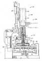
도 4는 도 2 및 도 3에서 나타낸 처리 시스템에 유용한, 기판(422)상에 금속층을 증착하고 평탄화하기 위한 장치(420)의 일 실시예의 횡단면도이며, 예를 들어 캐리어 조립장치(430)를 위한 장착 조립장치(mounting assembly)의 변형예들은 도 1의 처리 시스템(200)에서 이러한 조립장치를 사용하기 위해 이루어질 수 있다. 즉, 상기 캐리어는 캐루젤에 장착된다.4 is a cross-sectional view of one embodiment of an
상기 장치(420)는 일반적으로 스탠션(stanchion: 480)에 의해 부분 외장(434)의 위로 이동가능하게 지지되는 캐리어 조립장치(430)를 포함한다. 스탠션(480)과 외장(434)은 일반적으로 통상의 베이스(482) 위에 배치된다. 스탠션(480)은 일반적으로 베이스 지지부(484)와 승강기구(486)를 포함한다. 베이스 지지부(484)는 베이스(482)에서 수직으로 뻗어있고 그 축상에서 회전할 수 있기 때문에, 캐리어 조립장치(430)가 부분 외장(434) 상부로 이동되거나 다른 위치, 예를 들어 다른 외장들 또는 미도시된 다른 처리 시스템과의 인터페이스로 이동될 수 있다.The
승강기구(486)는 캐리어 조립장치(430)와 결합된다. 승강기구(486)는 일반적으로 부분 외장(434)에 대해 캐리어 조립장치(430)의 승강을 제어한다. 승강기구(486)는 볼 스크류, 땜납 스크류, 공압 실린더 등과 같은 선형 엑추에이터(488) 및 레일(492)를 따라 슬라이딩되는 가이드(490)를 포함한다. 레일(492)은 힌지(494)를 통해 베이스 지지부(484)와 결합되어 승강기구(486)의 레일(492)이 수평에 대해 약 90도 내지 60도 사이 범위의 각으로 제어될 수 있게 움직인다. 승강기구(486)와 힌지(494)는 기판(422)을 가지고 있는 캐리어조립장치(430)가 다양한 각도로 부분 외장(434) 안으로 하강하도록 할 수 있게 한다. 예를 들어, 외장(434) 내에 배치된 유체들과 접속될 때 기판(422) 위에 기포가 형성하는 것을 최소화하기 위하여, 기판(422)은 부분 외장(434)으로 삽입되는 동안은 소정의 각도가 되도록 하고, 그 내부에서는 수평 방향으로 회전될 수 있다.The
부분 외장(434)은 일반적으로 전해액 또는 다른 연마/증착 용액을 담을 수 있는 용기(container) 또는 전해액 셀을 형성한다. 외장(434)은 통상 애노드/캐소드(426), 확산판(diffuser plate: 444) 및 그 내부에 위치한 투과 디스크(428)를 포함한다. 연마 패드와 같은 투과 디스크(428)는 확산판(444)상의 전해액 셀에 배치되고 지지된다. 부분 외장(434)은 도금 화학(plating chemistry)에 적합한 플루오로폴리머(fluoropolymer), TEFLON, PFA, PE, PES 또는 다른 물질과 같은 플라스틱으로 만들어진 그릇 형상의 부재일 수 있다. 부분 외장(434)은 베이스(482) 아래로 뻗어있는 저면상의 샤프트(432)에 연결된다. 상기 엑추에이터는 수직축 x으로 부분 외장(434)을 회전시키기에 적합하다. 일 실시예에서, 샤프트(432)는 샤프트(432)에 형성된 다수의 포트(436)를 통해 유체를 부분 외장(434)으로 전달하는 중앙 통로를 형성하고 있다.Partial sheath 434 generally forms a container or electrolyte cell that can contain an electrolyte solution or other polishing / deposition solution. The sheath 434 typically includes an anode /
선택적으로, 부분 외장(434)은 샤프트(432)에 연결된 장착 플랫폼에 연결될 수 있다. 샤프트(432)는 베이스(482)에 배치되는 모터, 예로 스텝 모터와 같은 엑추에이터(미도시)와 연결된다.Optionally, the partial sheath 434 may be connected to a mounting platform connected to the shaft 432. The shaft 432 is connected to an actuator (not shown) such as a motor disposed on the
애노드/캐소드(426)는 외장(434)의 저면부에 상기 전해액에 잠길 수 있도록 위치한다. 상기 애노드/캐소드는 인가되는 (+)바이어스(애노드) 또는 (-)바이어스(캐소드)에 따라 애노드 또는 캐소드로써 수행할 수 있다. 예를 들어, 기판 표면상의 전해액에서 물질을 증착한다면, 애노드/캐소드(426)는 애노드로서 작용하고 상기 기판 표면은 캐소드로써 작용한다. 인가되는 바이어스에 의해 용해(dissolution)와 같이 기판 표면에서 물질을 제거한다면, 애노드/캐소드(426)는 캐소드로써 기능하고 웨이퍼 표면 또는 투과 디스크(428)는 용해 공정을 위한 애노드로써 작용할 수 있다.The anode /
애노드/캐소드(426)는 플레이트 형상의 부재, 관통하여 형성되는 다수의 홀을 갖는 플레이트 또는 투과할 수 있는 막 혹은 용기에 위치하는 다수의 조각(piece)일 수 있다. 애노드/캐소드(426)는 구리, 니켈, 알루미늄, 금, 은, 텅스텐 및 기판 위에 전기화학적으로 증착될 수 있는 다른 물질들과 같은, 증착되거나 제거될 수 있는 물질로 이루어진다. 적어도 일 실시예에서, 상기 애노드/캐소드는 구리 증착 또는 전기연마 공정을 위한 백금과 같은 증착 물질보다 비-소모적인 애노드/캐소드(426) 물질을 포함할 수 있다. 선택적으로, 증착 공정에서 애노드/캐소드(426)는 주기적인 교체를 필요로 하는 소모성 애노드/캐소드를 포함할 수 있다.The anode /
적어도 일 실시예에서, 애노드/캐소드(426)는 샤프트(432)의 유체 입구가 관통하여 배치되는 중심 개구부를 형성하는 링 형상이다. 애노드/캐소드(426)가 플레이트 형상인 실시예들에서, 이를 관통하여 전해액이 통과할 수 있도록 하는, 다수의 홀은 상기 애노드/캐소드를 관통하여 형성될 수 있다.애노드/캐소드(426)는 선택적으로 링 애노드/캐소드, 플레이트 애노드/캐소드, 또는 투과 챔버 혹은 다른 외장을 포함하는 도금 물질(plating material)을 담고 있는 챔버일 수 있다.In at least one embodiment, anode /
투과 디스크(428)는 유체 환경 및 처리 성능조건에 적합한, 연마 제품 또는 다른 형태의 볼륨 스페이서(volume spacer)일 수 있다. 투과 디스크(428)는 부분 외장(434)의 상단에 위치하고 확산판(444)에 의해 그 저면상에 지지된다. 예를 들어 구리 애플리케이션에서 구리 이온과 같은 금속 이온들은 투과될 수 없는 것에 반하여, 투과 디스크(428)는 전해액의 이온들이 투과할 수 있는 것이 바람직하다. 상기 금속 이온들은 투과 디스크(428) 상부에 위치하는 출구(42)를 갖는 유체 수송 라인(40)으로부터 공급될 수 있다. 투과 디스크(428)는 애노드/캐소드(426)와 인접 또는 연결되어 배치될 수 있다.
투과 디스크(428)는 가속기 및 압축기 침전 부산물과 같은 증착 부산물의 흐름을 방지하면서 전해액이 기판 표면으로 흐를 수 있도록 하는 충분한 크기와 조직의 다수의 구멍(pore)을 포함할 수 있다. 또한, 투과 디스크(428)는 벌크 용액에서 외장(434) 안으로 기판(422)과 투과 디스크(428) 사이의 틈에 새로운 전해액을 수송하기 위해 그 내부에 형성되는 홈들을 포함할 수 있다. 그러나, 투과 디스크(428)는 몇 가지 애플리케이션에서는 금속 이온들이 투과될 수 있다.
통상, 투과 디스크(428)는 폴리우레탄과 같은 중합체 물질로 구성되는 연마 패드와 같은 연마 제품을 포함한다. 사용될 수 있는 연마 패드의 예들로는, 그러나 그것에 국한됨이 없이, 애리조나 피닉스에 위치한 Rodel사의 IC 1000, IC 1010, Suba 시리즈 패드, Politex 시리즈 패드, MHS 시리즈 패드, 일본 Asahi의 PVDF 패드 또는 미네소타 미네아폴리스에 위치한 3M의 고정 연마 패드가 있다.Typically, the
상기 투과 디스크는 전기도금 증착 및 전기연마 공정을 위한 전도성 물질을 포함하는 연마 제품일 수 있다. 예를 들어, 전기연마 공정에서, 전도성 연마 제품은 연마 제품상에 전도성 경로를 제공하기 위해, 전도성 폴리머 혹은 그 내부에 내장 또는 형성되는 전도성 성분 혹은 물질(미도시)을 갖는 폴리우레탄과 같은 폴리머를 포함할 수 있다. 상기 전도성 성분은 상기 연마 제품에서 서로 전기적으로 연결되고 상기 기판이 상기 연마 제품과 연결될 때 기판 표면과 연결될 수 있다. 전도성 연마 물질의 다른 예들은 2001년 4월 24일자로 제출된 미국 가특허출원 시리얼 넘버 60/286,107에 명시되어 있고, 본 발명에서 언급되는 청구항 및 실시예들과 일치하는 범위에서 참조로 본 발명에 포함될 수 있다.The transmission disk may be an abrasive product comprising a conductive material for electroplating deposition and electropolishing processes. For example, in an electropolishing process, a conductive abrasive product may comprise a polymer, such as a polyurethane, having a conductive polymer or a conductive component or material (not shown) embedded or formed therein to provide a conductive pathway on the abrasive product. It may include. The conductive components may be electrically connected to each other in the abrasive article and to the substrate surface when the substrate is connected to the abrasive article. Other examples of conductive abrasive materials are set forth in US Provisional Patent Application Serial No. 60 / 286,107, filed April 24, 2001, and are incorporated herein by reference in the scope consistent with the claims and embodiments mentioned herein. May be included.
전도성 연마 제품이 상기 투과 디스크에 사용된다면, 상기 전도성 연마 제품은 전원(미도시)과 전기적으로 연결될 수 있고, 전기 기반의 용해 공정에서 애노드로서 사용될 수 있다. 선택적으로, 상기 연마 제품은 전기증착 공정을 위한 폴리우레탄과 같은, 절연 물질 혹은 낮은 컨덕턴스 물질을 형성할 수 있다.If a conductive abrasive product is used in the transmission disk, the conductive abrasive product can be electrically connected to a power source (not shown) and used as an anode in an electrical based melting process. Optionally, the abrasive article may form an insulating material or a low conductance material, such as polyurethane for the electrodeposition process.
전력 공급기(미도시)는 장치(420)를 통해 상기 기판 표면과 연결된다. 상기 전력 공급기는 일정한 전류 동작과 일정한 전압 동작을 스위치하는 제어 회로를 포함할 수 있다. 상기 전력 공급기의 제어 회로는 출력의 극성을 제어한다. 일 실시예에서, 상기 전력 공급기는 제 1 주기동안 일정한 전류 출력과 제 2 주기동안 일정한 전압 출력을 반복하도록 구성된 출력 파장과 같이, 다양한 출력 파장을 형성하기 위해 프로그래밍이 될 수 있는 스위칭 회로를 포함한다. 본 발명은 애노드와 캐소드간의 시간-가변 전위와 같은 출력 파장을 형성할 수 있는 다양한 디자인의 전력 공급기, 또는 애노드 또는 캐소드로서 수행하는 장치를 이용할 수 있음을 예시하며, 어떤 특정 디자인의 전력 공급기에 한정되지 않는다. 예를 들어, 상기 전력공급기는 기판 표면에 시변(time varying) 애노드 전위를 인가하도록 적용될 수 있다.A power supply (not shown) is connected to the substrate surface via
확산판(444)은 부분 외장(434)의 투과 디스크(428)에 대한 지지를 제공한다. 확산판(444)은, 그 내부에 매달 수 있는, 스크류와 같은 패스너, 또는 스냅 혹은 외장에 억지 끼워 맞춤(interference fit)과 같은 다른 수단 등을 이용하여 부분 외장(434)에 고정될 수 있다. 확산판(444)은 예를 들어, 플루오로폴리머, PE, TEFLON®, PFA, PES, HDPE, UHMW 등의 플라스틱과 같은 물질로 이루어질 수 있다. 적어도 일 실시예에서, 확산판(444)은 그 내부에 형성되는 다수의 홀 또는 채널(46)을 포함한다. 홀(446)들은 유체가 관통하여 흐를 수 있고 투과 디스크(428)를 통해 기판(422)으로 전해액을 균일하게 분배할 수 있는 크기로 형성된다. 투과 디스크(428)는 유체 환경 및 처리 조건에 적합한 접착제를 이용하여 확산판(444)에 고정될 수 있다. 확산판(444)은 바람직하게는 애노드/캐소드(426)로부터 이격되어, 더 넓은 처리 윈도우를 제공하여 상기 애노드/캐소드 영역으로의 도금 막 두께의 민감성을 감소시킬 수 있고, 예를 들어 독일의 Raschig사로부터 상업적으로 이용할 수 있는 비스(3-sulfopropyl) 2황화물, C6H12Na2O6S4와 같이 가속기로부터 저하되는 모노-황화물 화합물인, 가속기 및 압축기 분해 부산물을 투과 디스크(428)와 기판(422) 사이에 형성되는 메인 플레이팅 볼륨(428)으로부터 분리시킬 수 있다.The
도시되지 않았지만, 막은 외장(434)에 삽입되고 기판 표면상의 입자들로써 증착됨으로써, 애노드/캐소드 막으로부터 형성되는 입자들을 포함하기 위해 애노드/캐소드(426)와 투과 디스크(428) 사이에 배치될 수 있다. 예를 들어, 상기 막은 전해액이 흘러 투과할 수 있지만, 통상 상기 애노드/캐소드 표면상의 가속기 및 압축기 저하 부산물은 투과할 수 없다.Although not shown, the film can be placed between the anode /
기판 캐리어 또는 헤드 조립장치(430)는 투과 디스크(428) 상부에 이동 가능하게 위치한다. 기판 캐리어 조립장치(430)는 투과 디스크(428) 위로 수직으로 이동할 수 있고, 이의 측면으로 이동할 수 있으며, 예를 들어 캐리어 조립장치(430)는 수직축 y에 대해 회전할 수 있다. 상기 부분 외장 및 헤드 조립장치의 x, y축은 투과 디스크(428)와 기판 캐리어 조립장치(430) 간에 궤도 운동(orbital motion)을 제공하기 위해 각각 나란히 설치된다. 상기 궤도 운동은 투과 디스크(428)와 기판 캐리어 조립장치(430) 간에 타원의 상대성 운동으로서 본 발명에서 폭넓게 언급된다. 기판 캐리어 조립장치(430)는 투과 디스크(428)를 향하여 아랫방향으로 마주한 증착 표면을 갖는 기판(422)을 붙잡는다. 선택적으로, 투과 디스크(428)는 병진 또는 선형 상대성 운동, 및 회전 혹은 원형 회전 상대성 운동으로 기판 캐리어 조립장치(430)로 이동될 수 있는 표면을 포함할 수 있다.The substrate carrier or
기판 캐리어 조립장치(430)는 일반적으로 구동 시스템(468), 헤드 조립장치(478) 및 시트 조립장치(476)를 포함한다. 구동 시스템(468)은 스탠션(480)의 가이드(490)와 결합된다. 구동 시스템(468)은 시트 조립장치(476)를 지지하기 위해 파워 헤드(456)로부터 연장되는 열(column:470)을 포함한다. 파워 헤드(456)는 전기 또는 공압 모터일 수 있고, 일반적으로 중심축을 따라 열(470)의 회전을 제공한다. 구동 시스템(486)은 열(470) 내에 배치되어 헤드 조립장치(478)와 결합되는 엑추에이터(454)를 포함한다. 땜납 스크류, 공압 실린더 혹은 다른 선형 엑추에이터일 수 있는 상기 엑추에이터(454)는 헤드 조립장치(478)가 시트 조립장치(476)에 대해 이동될 수 있도록 한다.The
시트 조립장치(476)는 그립퍼 플레이트(472) 둘레의 극 어레이에 배치되는 다수의 그립퍼 핑거(474)를 포함한다. 그립퍼 플레이트(472)는 열(470)에 결합되어 구동 시스템(468)과 함께 이동한다. 일 실시예에서, 3개의 그립퍼 핑거(474)가 제공된다. 그립퍼 핑거(474)는 일반적으로 베이스 부재(466), 연장부(464) 및 접촉 핑거(462)를 포함한다. 접촉 핑거(462)는 연장부(464)에 대한 각도로 배치된다. 연장부(464)는 베이스 부재(466)와 결합된다. 베이스 부재(466)는 그립퍼 플레이트(472)와 회전 가능하게 결합된다. 베이스 부재(466)는 그립퍼 플레이트(472)의 홀과 일치하는 구멍을 포함한다. U자형 핀 또는 다른 샤프트 부재는 상기 홀 및 구멍을 통해 배치되어 그립퍼 핑거(474)가 그립퍼 플레이트(472)에 대해 회전할 수 있도록 한다.The
엑추에이터(460)는 연장부(464)와 그립퍼 플레이트(472) 사이에 결합된다. 엑추에이터(460)는 개폐되는 위치 사이에서 그립퍼 핑거(474)를 이동시킨다. 스프링(458)은 그립퍼 핑거(474)가 하나의 위치를 향해 경사지도록(bias) U자형 핀 상에 부가적으로 배치될 수 있다. 접촉 핑거(462)가 내향(inward)으로 이동될 때, 각 접촉 핑거(462)의 끝단에 배치되는 노치(notch: 452)는 전달 로봇(미도시)으로부터 기판(422)을 수납하기 위해 적용되는 시트(450)를 형성한다. 상기 내향 위치에서, 연장부(464)는 기판(422)과 로봇이 서로간에 지나칠 수 있도록 서로 일정 거리를 두고 배치된다.The
또한, 도시되지는 않았지만, 컴퓨터 기반의 컨트롤러는, 시스템이 장치(420)에서 기판 전달 또는 기판 연마와 같은 시스템상의 하나 이상의 처리 단계를 수행하도록 하기 위해, 장치(420)에 연결될 수 있다.Also, although not shown, a computer-based controller may be coupled to the
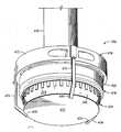
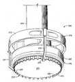
도 5는 헤드 조립장치(478)의 일 실시예를 나타낸다. 헤드 조립장치(478)는 일반적으로 하우징(502), 스템(stem: 504), 지지판(506) 및 다수의 기판 클램프(520)(하나의 클램프만 도시됨)를 포함한다. 일반적으로, 하우징(502)은 일측단에서 엑추에이터(454)와 결합되고 타측단은 플렌지(flange:508)에서 종결되는 중공 샤프트(528)를 포함한다. 플렌지(508)는 중심 캐비티(512)가 형성된 하향 연장 립(510)을 갖는다.5 shows one embodiment of the
지지판(506)은 중심 캐비티(512)에 배치된다. 지지판(506)은 일측면(514)과 타측면(516)을 갖는다. 기판(422)은 처리 동안에 일측면(514)에 인접하여 배치된다. 일측면(514)은 일측면(514)과 인접한 기판(422)을 지탱하기 위해 그 내부에 배치된 하나 이상의 진공포트(518)를 부가적으로 포함할 수 있다.The
스템(504)은 지지판(506)의 타측면(516)과 결합된다. 스템(504)은 일반적으로 지지판(506)의 수직방향이다. 스템(504)은 지지판(508)의 일측면(514) 혹은 헤드 조립장치(478)의 다른 부분들에 진공 또는 유체를 제공하기 위해, 그 내부에 배치되는 통로를 포함할 수 있다.The
기판 클램프(520)는 통상 구리와 같은 전도성 물질로 이루어진다. 기판 클램프(520)는 각각의 기판 클램프(520)와 전기적으로 연결된 전도성 링(522)과 결합된다. 스크류는 통상 전도성 링(522)에 기판 클램프(520)를 고정시키는데, 다른 패스너 혹은 고정 방법이 이용될 수도 있다. 전도성 링(522)은 일반적으로 하우징(502)을 통과해 연결되는 리드(lead: 526)에 의해 링(522)과 결합되는 전원(미도시)을 통해 링(522)이 전기적으로 바이어스될 수 있도록 하는 단자(524)를 포함한다.The
도 6a는 지지판(506)의 일측면(514)로부터 연장되는 기판 클램프(520)의 부분 사시도를 나타낸다. 기판 클램프(520)는 지지판(506) 주변에서 극 어레이에 배치된다. 일 실시예에서, 클램프(520)는 지지판(506)에 대해 이동할 수 있으므로, 클램프(520)가 지지판(506)에서 돌출되는 거리를 조정할 수 있다. 일반적으로, 기판 클램프(520)는 지지판(506) 주변에서 동일하게 이격되는 다수의 제 1 클램프(402)와 다수의 제 2 클램프(404)를 포함한다. 제 1 및 제 2 클램프(402, 404)는 주변에서 배열(시퀀스)이 번갈아 위치하고, 그립퍼 핑거(474)가 이들 사이를 지나갈 수 있도록 이격된다. 제 1 클램프(402)는 통상 사각형상이고, 기판(422)의 직경에 일치하도록 이의 폭에 대하여 선택적으로 구부러져 있다. 또한, 제 2 클램프(404)도 통상 사각형상이며, 기판(422)의 직경에 일치하도록 이의 폭에 대하여 선택적으로 구부러져 있다. 제 1 클램프 및 제 2 클램프(402, 404)는 상기 기판과 접촉되는 내면(406)을 갖는다.6A shows a partial perspective view of the
도 6a 및 도 6b에 도시된 것처럼, 클램프(520)는 기판(422)이 펼쳐질 때, 이들 사이로 통과할 수 있도록 바깥쪽으로 비스듬히 있다. 클램프(520)의 내면에 배치되는 범프(410)는 지지판(506)의 외면(412)과 접촉된다. 범프(410)는 클램프(520)가 확장될 때 바깥쪽으로 벌어지도록 한다. 선택적으로, 지지판(506)은 지지판(506)의 표면(412) 위에서 범프(410)가 부드럽게 움직이도록 하는 챔버(414)를 포함할 수 있다. 하우징(502)은 클램프(520)를 내향하게 하는 클램프(520)의 외향 방사로 배치되는 경사 부재(bias member)를 포함한다. 일 실시예에서, 상기 경사 부재는 데탕트 핀(detente pin: 416)이다.As shown in FIGS. 6A and 6B, the
제 2 클램프(404)는 끝단 근처의 접촉 표면에 형성된 노치(418)를 포함한다. 노치(418)는 통상 기판(422)의 두께보다 길이가 더 긴 저면(620)을 갖는다. 제 1 클램프(604)의 끝단과 최근접한 노치(418)의 벽(419)은 베벨(bevel) 또는 라운드형 테두리의 기판(422)과 접촉되도록 모서리가 깎이거나(chamfer) 각진다.The
도 7a 내지 도 7d는 캐리어 조립장치(430)에 로딩되는 기판(422)을 나타낸다. 도 7a에서, 그립퍼 핑거(474)는 미도시된 로봇으로부터 기판(422)을 수납하는 시트(450)를 형성하기 위해 회전된다. 헤드 조립장치(478)는 시트 조립장치(476)와 인접한 제 1 위치(592)에 배치된다. 기판 클램프(522)는 지지판(508)의 일측면(514)에서 완전히 확장된다. 상기 로봇이 그립퍼 핑거(474)의 시트(450)에 기판(422)을 남기고 사라지면, 헤드 조립장치(478)는 제 2 위치(504)로 연장되어 기판 클램프(522)들 사이의 시트(450)에 지탱되는 기판(422)을 로드한다(도 7b 참조). 제 1 클램프(402)는 헤드 조립장치(478)에 대해 기판(422)을 중심에 위치시킨다.7A-7D show a
그리고, 클램프(522)는 지지판(508)을 향해 수축된다. 제 2 클램프(404)의 각진 벽(419)은 기판(422)의 베벨 테두리와 연결되고 지지판(508)에 대하여 기판(422)을 잡아당긴다. 각진 벽(419)과 기판(422) 사이의 상호작용은, 부가적으로 제 2 클램프(404)가 데탕트 핀(416)에 대해 바깥쪽으로 구부러게 하며, 상기 기판 주변에 대해 노치(418)의 저면(420)을 대체한다. 구부러진 제 2 클램프(404)와 데탕트 핀(416)은, 지지판(508)에 대하여 기판(422)을 붙잡기 위해, 제 2 클램프(404)를 안쪽으로 가압하기 위해 결합하며, 클램프(404)와 기판(422) 사이에서 좋은 전기 접촉을 제공한다(도 7c 및 도 7d 참조).Then, the
도 5로 돌아가서, 전도성 링(522)은 하우징(502)과 지지판(506) 사이의 중심 캐비티(512)에 배치되는 장착판(530)에 고정된다. 장착판(530)은 일반적으로 지지판(506)에 대해 이동가능하므로, 거리-거리는 기판 클램프(520)가 상기 지지판의 일측면(514)을 넘어 연장되는 거리-를 조정할 수 있다. 일반적으로, 장착판(530)은 이들 사이에 위치한 스프링(532)에 의해 지지판(506)으로부터 떨어져 기울어진다.Returning to FIG. 5, the
장착판(530)과 기판 클램프(520)의 움직임을 용이하게 하기 위하여, 장착판(530)은 스템(504) 주위에 이동 가능하게 배치되는 슬리브(534)와 결합된다. 슬리브(534)는 오-링(538)과 같은 봉인물에 의해 일단에서 스템(504)에 대해 밀봉되는 제 1 직경부(536)를 갖는다. 슬리브(534)는 스템(504)의 협부(narrower portion: 542)와 접촉하는 더 작은 제 2 직경부(540)를 갖는다. 스템(504)의 협부(542)는 오-링(552)을 통해 슬리브(534)에 부착되므로, 스템(504)과 슬리브(534) 사이에 피스톤 챔버(544)를 형성할 수 있다. 공기와 같은 유체가 챔버(544)에 인가되거나 진공화되면, 결과적으로 슬리브(534)와 스템(504) 사이에 힘이 인가되어 슬리브(534)가 이동할 수 있게 하기 때문에, 기판 클램프(520)를 이동시킬 수 있다.In order to facilitate movement of the mounting
슬리브(534)의 외면부(546)에는 암나사산이 형성되고, 장착판(530)에 배치된 해당 수나사산부(548)와 결합된다. 장착판(530)과 슬리브(534) 사이의 나사산 수를 조정하여, 기판 클램프(520)가 소정 양만큼 지지판(506)으로부터 돌출될 거리를 설정할 수 있다. 장착판(530)이 슬리브(534)에 대해 돌발적으로 회전되는 것을 방지하기 위해, 장착판(530)의 설정 스크류(550)를 바짝 조일 수 있다.A female thread is formed on the
도 8은 기판 캐리어 헤드 조립장치(800)의 다른 실시예의 부분도를 나타낸다. 기판 캐리어 헤드 조립장치(800)는 접촉판(802)이 지지판(804)에 배치되는 점을 제외하고는 전술한 기판 캐리어 조립장치(430)와 대체로 유사하다. 일반적으로, 접촉판(802)은 지지판(804)의 일측면(806)상에 배치된다. 접촉판(802)은 전도성 물질로 이루어지고, 처리 동안에 기판(422)을 바이어스하는데 이용된다. 접촉판(802)은 지지판(804)의 타측면(812)상에 배치된 단자(810)와 전기적으로 결합된다. 단자(810)는 기판(422)을 바이어스하는데 사용되는 리드(808)를 통해 접촉판(802)이 전원(미도시)과 결합되는 것을 용이하게 한다.8 shows a partial view of another embodiment of a substrate
접촉판(802)은 통상 기판(422)의 테두리에 인접하여 위치한다. 접촉판(802)은 전압 바이어스와 같은 바이어스를 기판에 직접 접속시키거나, 기판 후면의 일부로 기판 테두리 주위를 둘러싸는 기판 표면상에 배치된 전도성 시드층(seed layer: 820)에 접속시킨다.The
도 9는 기판 캐리어 헤드 조립장치(900)의 다른 실시예를 나타낸다. 기판 캐리어 헤드 조립장치(900)는 하우징(902)의 저면부에 배치되는 개구부(906)와 함께 중심 캐비티(904)를 형성하는 하우징(902)과 하우징(902)의 종단면(920)에 배치되는 적어도 하나의 포트(908)를 포함한다. 포트(908)는 로봇(미도시)으로부터 기판(422)을 캐비티(904) 내에 수평으로 수납할 수 있는 크기로 형성된다.9 shows another embodiment of a substrate carrier head assembly 900. The substrate carrier head assembly 900 is disposed in the
동작 샤프트(actuating shaft: 910)는 하우징(902)에 배치되고, 상기 기판 캐리어에 배치되거나 상기 기판 캐리어에 연결된 모터(미도시)를 통해 하우징(902)의 개구부(906)를 향해 지지판(922)을 동작시킬 수 있다. 지지판(922)은 상기 로봇으로부터 기판을 수납하고, 수평으로 이동되는 방식으로 상기 기판을 아래로 향하도록 고정시킨다.An
지지판(922)은 지지판(922)의 일측면(924)에 배치된 접촉판(916)을 포함한다. 접촉판(916)은 전도성 물질로 이루어지고 처리 동안 기판(422)을 바이어스하는데 이용된다. 접촉판(916)은 지지판(922)의 타측면(928)에 배치된 단자(926)와 전기적으로 결합된다. 단자(926)는 기판(422)을 바이어스하는데 사용되는 리드(930)를 통해 접촉판(916)이 전원(미도시)과 연결되는 것을 용이하게 한다. 접촉판(916)은 일반적으로 기판(422)의 테두리에 인접하여 위치한다. 접촉판(916)은 전압 바이어스와 같은 바이어스를 기판에 직접 접속시키거나, 상기 기판 후면의 일부로 상기 기판 테두리 주위를 감싸는 상기 기판 표면상에 배치되는 전도층으로 접속시킨다.The
개구부(906) 둘레의 접촉링(912)은 동작 샤프트(910)가 접촉링(912)에 대해 기판(422)을 가압할 때 기판(422)을 지지하는 기판 지지부(914)를 포함한다. 기판 지지부(914)는 기판 표면과 연속적으로 접촉하기 위한 환형 링을 포함하거나, 접촉링(912) 주위에 원형으로 배치되는 일련의 접점들을 포함할 수 있으며, 그 위에 배치된 기판(422)과의 접촉이 증가한다. 접촉링(912)은 상기 기판 표면과 프로세싱 셀에 배치된 평탄한 연마 제품 사이의 접촉을 감소시킨다. 따라서, 상기 기판 캐리어 조립장치는, 연마 제품이 없는 전기화학적 증착 및 전기화학적 용해 공정 또는 사용자가 기판의 한정된 연마를 원하는 경우에 사용될 수 있다. 도시되지 않았지만, 기판 지지부(914)는 기판(422)을 바이어스하는데 사용되는 리드(930)를 통해 전원(미도시)과 결합될 수 있고, 접촉링(912)은 절연물질을 포함한다.The
도 10a는 연마 헤드(430)의 다른 실시예를 개념적으로 나타내는 횡단면도이다. 연마 헤드(430)는, 전도성 연마 제품과 같은 전도성 투과 디스크가 애노드 용해 공정에서 사용되고 있는 본 발명의 실시예에서, 이용될 수 있다. 연마 헤드(430)는 통상 캐리어 플레이트(1002), 커버(1004) 및 지지링(1006)을 포함한다. 일 실시예에서 팽창 부레(bladder)를 포함할 수 있는 캐리어 플레이트(1002)는, 예를 들어, 도 1의 스테이션(106, 102)에 배치될 수 있는, 연마 제품에 대하여 기판(1014)을 가압한다. 지지링(1006)은 캐리어 플레이트(1002)를 둘러싸고, 처리 동안 기판(1014)이 연마 헤드(1030) 아래에서 외부로 측면으로 이동하는 것을 방지한다.10A is a cross-sectional view conceptually illustrating another embodiment of a polishing
캐리어 플레이트(1002)와 지지링(1006)은 축방향으로 서로에 대해 이동할 수 있다. 캐리어 플레이트의 저면과 지지링(1006) 사이의 상대 거리(1014)는 조정될 수 있기 때문에, 기판(1014)이 지지링(1006) 넘어로 연장된 상기 상대 거리 또는 지지링(1006)이 투과 디스크 또는 연마 제품에 가하는 압력의 양을 설정할 수 있다.The
도 10b의 부분 개념도로서 나타낸 연마 헤드의 선택적 실시예에서, 지지링(1006)은 굴곡부(flexure)에 의해 연마 헤드(430)와 이동 가능하게 결합된다. 탄력성 금속 시트 또는 폴리머일 수 있는 굴곡부(1008)는 지지링(1006)과 캐리어 플레이트(1002) 사이에 배치되어 서로간에 축상으로 이동될 수 있게 한다. 커버(1004)에 배치된 피스톤(1010)은 지지링(1006)에 결합된다. 유체를 피스톤(1010)에 공급하여(혹은 피스톤(1010)으로부터 제거하여), 축방향으로 지지링(1006)을 가압하므로, 거리(1014)를 둘 수 있다.In an optional embodiment of the polishing head shown as a partial conceptual view of FIG. 10B, the
본 발명에서 언급되는 공정을 수행하는데 사용되고, 도 2 및 도 3에서 나타낸 바와 같은 처리 시스템(200)에서 사용되거나 적용될 수 있는, 다른 장치는 2001년 1월 26일자로 제출된 미국특허출원 시리얼 넘버 09/770,559에 더 상세히 언급되어 있으며, 각각이 참조로 본 발명에 포함될 수 있다.Another apparatus, which may be used to perform the process referred to in the present invention and may be used or applied in the
도 11a 내지 도 11d는 기판(1122)에 금속층을 증착 및 평탄화하기 위한 장치(1120)의 실시예들의 개념적 횡단면도이다.11A-11D are conceptual cross-sectional views of embodiments of
도 11a는 연마 물질의 롤러(1128)를 이용하여 기판(1122)의 표면을 연마하는데 적용되는 장치(1120)를 나타낸다. 연마 물질은 전도성 물질, 절연 물질 및 절연 물질 안에 배치되는 전도성 성분으로 이루어질 수 있고, 및/또는 본 발명에서 언급된 것처럼 연마재 소자 또는 입자를 포함할 수 있다.11A shows an
장치(1120)는 부분 외장(1134) 상에 위치할 수 있는 캐리어 헤드 조립장치(1130)를 포함한다. 부분 외장(1134)은 전해액 혹은 다른 연마/증착 용액을 담을 수 있는 용기 또는 전해액 셀을 형성한다. 외장(1134)은 통상 애노드/캐소드(1126) 및 그 내부에 배치되는 연마 물질로 이루어진 롤러(1128)를 포함한다. 부분 외장(1134)은 모터(예, 스텝 모터)와 같은 엑추에이터(미도시)에 연결되는 장착 플랫폼과 연결될 수 있다. 상기 엑추에이터는 수직축 x에 대해 부분 외장(1134)을 회전시키는데 적용된다. 일 실시예에서, 샤프트(1140)는 유체가 부분 외장(1134)으로 전달되는 관통 중앙 통로를 형성하고 있다. 선택적으로, 유체는 외장(1134)에 인접 배치되는 입구(1140)를 통해 부분 외장(1134)으로 전달된다.
애노드/캐소드(1126)는 외장(1134)의 벽(1136)에 배치된 애노드/캐소드 링을 포함할 수 있고, 증착 및 애노드 용해를 수행하기 위해 기판(1122) 및/또는 롤러(1128)가 바이어스를 갖도록 적용될 수 있다. 선택적으로, 애노드/캐소드(1126')는 전해액에 잠길 수 있는 외장(1134)의 저면부에 위치할 수 있다. 애노드/캐소드(1126)는 적용되는 (+) 바이어스(애노드) 또는 (-) 바이어스(캐소드)에 따라 애노드 또는 캐소드로서 수행될 수 있다. 예를 들어, 인가되는 바이어스를 통한 애노드 용해에 의해 기판 표면에서 물질을 제거할 때, 애노드/캐소드(1126)는 캐소드로서 작용되고 웨이퍼 표면 또는 투과 디스크(1128)는 용해 공정을 위한 애노드로서 작용할 수 있다. 위어(weir: 1145)는 전해액을 막아 두기 위해 외장(1134)의 외면에 배치될 수 있고, 샤프트(1140)를 통해 필터링되고 재순환(recycle)되거나 배치될 수 있다.The anode /
기판 캐리어 또는 헤드 조립장치(1130)는 롤러(1128) 상부에 이동 가능하게 위치한다. 기판 캐리어 조립장치(1130)는 롤러(1128) 상부에 수직으로 이동할 수 있고 측면상으로 이동할 수 있으며, 예를 들어 캐리어 조립장치(430)는 수직축 y에 대해 회전할 수 있다. 부분 외장 및 헤드 조립장치의 x, y축은 각각 롤러(1128)와 기판 캐리어 조립장치(1130) 간의 궤도 운동을 제공하기 위해 오프셋된다.The substrate carrier or the
기판 캐리어 조립장치(1130)는 일반적으로 롤러(1128) 아래로 향하는 증착 표면을 갖는 기판(1122)을 지탱한다. 기판 캐리어 조립장치(1130)는 외장(1134)에 수직 위치로 기판을 제공하도록 적용될 수 있다. 롤러(1128)는 상기 기판 표면을 연마하기 위해 기판 표면과 평행하게 회전될 수 있는 연마 물질로 된 실리더형 표면을 포함한다. 롤러(1128)는 "밀어내기(sweep)"하거나 상대성 평행 운동, 즉 병진 또는 선형 상대성 운동으로 기판을 연마하기 위해 기판의 표면 전체로 이동할 수 있다. 더 나아가, 롤러(1128)는 기판의 표면 전체에 대해 수평으로 회전하거나, 기판 표면에 접촉하기 위한 부가 물질을 노출하기 위해 수평으로 회전할 수 있다.The
롤러(1128)의 일 실시예에서, 상기 롤러는, 각각의 기판 직경에 대해서, 상기 기판 직경에 약 1/4인치(1/4") 내지 약 1인치(1")의 부가 폭을 더한 정도의 세로 폭을 갖도록 적용된다. 상기 롤러 직경은 사용자의 요구조건과 시스템의 크기에 따라 어떤 값이 될 수 있다. 예를 들어, 약 3인치 내지 약 4인치의 직경을 갖는 롤러가 본 발명에서 언급된 전기화학적 프로세싱 셀에 사용될 수도 있다.In one embodiment of
상기 롤러는 연마시 약 500rpm 이하, 예를 들어 약 10rpm 내지 약 200rpm의 속도로 축상으로 혹은 수직으로 회전할 수 있다. 상기 롤러는 기판 표면의 효과적인 연마를 보장하기에 충분한 속도로, 예를 들어 초당 약 1/2인치(1/2"), 기판의 표면에 대해 이동할 수 있다. 도 11b는 연마시 서로 접촉하는 기판(1122)과 연마 물질의 롤러(1128)를 갖는 장치(1120)를 나타내는 도 11a의 개념적 측면도이다. 상기 기판은 연마될 표면이 아래를 향하도록 수평으로 위치하고, 외장(1134)으로 하강되며, 연마 공정을 위한 연마 물질의 롤러(1128)와 접촉하도록 위치한다.The roller may rotate axially or vertically at a speed of about 500 rpm or less, for example from about 10 rpm to about 200 rpm when polished. The rollers can move at a speed sufficient to ensure effective polishing of the substrate surface, for example about 1/2 inch (1/2 ") per second, relative to the surface of the substrate. Is a conceptual side view of Fig.
도 11c는 장치(1120)의 다른 실시예의 개념적 측면도이다. 도 11c에서 나타낸 실시예에서, 기판(1122)은 외장(1134) 내부의 전해액에서 위를 향하여 배치된다. 그리고, 연마 물질의 롤러(1128)는 기판 표면의 상부와 그 전체에 위치되어, 기판 표면으로부터 물질을 제거하기 위해 기판 표면 전체에 대한 기계적 활동을 제공한다.11C is a conceptual side view of another embodiment of the
도 11d는 장치(1120)의 다른 실시예의 개념적 측면도이다. 도 11d에서 나타낸 실시예에서, 기판(1122)은 외장(1134) 내부의 전해액에서 아래를 향하여 수직으로 배치된다. 전도성이 있을 수 있는, 연마 물질로 된 하나 이상의 롤러(1128)는 일렬로 위치하여 기판 표면에서 물질을 제거하기 위해 기판 표면 전체에 대한 기계적 활동을 제공한다.11D is a conceptual side view of another embodiment of the
전술한 시스템 및 장치의 실시예들의 제어를 용이하게 하기 위해, 컴퓨터 기반의 컨트롤러는 CPU(미도시)를 포함할 수 있고, CPU는 다양한 챔버 및 서브프로세서들을 제어하기 위한 산업 설비에 사용될 수 있는 어떤 형태의 컴퓨터 프로세서들 중 하나일 수 있다. 메모리(미도시)는 CPU와 결합된다. 상기 메모리 혹은 컴퓨터로 리드할 수 있는 매개체는 랜덤 액세스 메모리(RAM), 롬(ROM), 플로피 디스크, 하드 디스크 또는 어떤 다른 형태의 유무선 디지털 저장장치와 같이 하나 이상의 리드 가능한 메모리일 수 있다. CPU를 통해 정보 저장 및 명령이 실행된다.To facilitate control of the embodiments of the systems and apparatus described above, a computer based controller may include a CPU (not shown), which may be used in an industrial facility to control various chambers and subprocessors. It may be one of the computer processors in the form. The memory (not shown) is coupled with the CPU. The memory or computer readable medium may be one or more readable memories, such as random access memory (ROM), ROM, floppy disk, hard disk or any other type of wired or wireless digital storage device. Information storage and instructions are executed via the CPU.
지원 회로는 종래의 방식으로 프로세서를 지원하기 위해 CPU와 결합된다. 이러한 회로들은 캐시, 전력 공급기, 클록회로, 입출력 회로 및 서브시스템 등을 포함하고, 키보드, 트랙볼, 마우스, 컴퓨터 모니터, 프린터 및 플로터와 같이 컨트롤러와 함께 사용되는 입력장치들을 포함할 수 있다. 이러한 컨트롤러들은 통상 개인용 컴퓨터로서 알려져 있다; 그러나, 본 발명은 개인용 컴퓨터에 한정되지 않으며 워크스테이션, 미니컴퓨터, 메인프레임 및 슈퍼컴퓨터로 구현될 수 있다.The support circuitry is coupled with the CPU to support the processor in a conventional manner. Such circuits include caches, power supplies, clock circuits, input / output circuits and subsystems, and the like, and may include input devices used with the controller, such as keyboards, trackballs, mice, computer monitors, printers, and plotters. Such controllers are commonly known as personal computers; However, the invention is not limited to personal computers and can be implemented with workstations, minicomputers, mainframes and supercomputers.
공정, 예를 들면 이하에서 언급되는 증착 및 연마 공정은 통상의 소프트웨어 루틴으로써, 메모리에 저장된다. 또한, 상기 소프트웨어 루틴은 CPU를 통해 제어되는 하드웨어로부터 떨어져 위치하는 제 2 CPU(미도시)에 의해 저장 및/또는 실행될 수 있다.Processes, such as the deposition and polishing processes mentioned below, are stored in memory as conventional software routines. The software routine may also be stored and / or executed by a second CPU (not shown) located away from hardware controlled via the CPU.
본 발명의 공정은 소프트웨어로서 구현되는 것으로서 언급하지만, 본 발명에 명시되는 방법 단계들의 일부 또는 전부는 소프트웨어 컨트롤러 뿐만 아니라 하드웨어에서 수행될 수 있다. 따라서, 본 발명은 컴퓨터 시스템에서 실행되는 소프트웨어, 구체적인 응용 집적회로로서의 하드웨어 또는 다른 형태의 하드웨어 구성, 혹은 소프트웨어 및 하드웨어의 조합으로 구현될 수 있다.Although the process of the present invention is referred to as being implemented as software, some or all of the method steps specified in the present invention may be performed in hardware as well as in a software controller. Thus, the present invention may be implemented in software running on a computer system, in hardware as a specific application integrated circuit, or in another form of hardware configuration, or a combination of software and hardware.
평탄화 공정Planarization process
본 발명에서 언급되는 방법의 실시예들은 전기화학적 제거 기술 및 연마 기술을 이용하여 기판 표면을 평탄화하기 위해 제공된다. 일 실시예에 따른 기판 처리 방법은 부식 억제제, 균염제, 점착 형성제 또는 이들의 조합을 포함하는 전해액에 기판을 위치시키는 단계, 기판에 애노드 바이어스를 인가하는 단계, 상기 전해액에서 상기 기판을 연마하는 단계 및 상기 기판 표면에서 물질을 제거하는 단계를 포함한다. 상기 공정은 단계들을 포함하는 것으로서 본 발명에서 언급되지만, 상기 단계들은 서로 분리될 필요가 없고 동시에 분리될 필요도 없다.Embodiments of the method referred to herein are provided for planarizing the substrate surface using electrochemical removal techniques and polishing techniques. According to one or more exemplary embodiments, a method of treating a substrate includes positioning a substrate in an electrolyte including a corrosion inhibitor, a leveling agent, a tackifier, or a combination thereof, applying an anode bias to the substrate, and polishing the substrate in the electrolyte. And removing material from the substrate surface. Although the process is mentioned in the present invention as including steps, the steps need not be separated from each other and need not be separated at the same time.
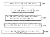
도 12는 본 발명의 일 실시예에 따른 공정 단계들을 나타내는 흐름도이다. 상기 공정은 기판 캐리어 조립장치(430)에 기판을 위치시키고, 단계 1300에서 전극 및 전해액을 포함하는 부분 외장(434)에 기판을 위치시킴으로써 시작된다. 상기 기판은 전원(미도시)과 전기적으로 연결되고 각각 캐소드 또는 애노드로 수행되는 전극으로써 기판 처리시 애노드 또는 캐소드로 수행한다. 선택적으로, 투과 디스크(428)는 연마 기술과 같은 처리 동안 상기 기판에 전력을 전기적으로 전도하는 전도성 연마 물질일 수 있다.12 is a flowchart illustrating process steps in accordance with an embodiment of the present invention. The process begins by placing the substrate in the
상기 기판은 외장의 전해액에 배치되어 적어도 상기 전해액과 접촉되는 기판 표면을 갖고, 일 실시예에서, 전체 기판이 상기 전해액에 침수될 수 있다. 상기 전해액은 유체 수송라인(440) 및/또는 도 4에 나타낸 바와 같은 투과 디스크(428) 아래의 유체 입구를 통해 부분 외장(434)에 제공될 수 있다.The substrate has a substrate surface disposed in contact with the electrolyte and at least in contact with the electrolyte, and in one embodiment, the entire substrate may be submerged in the electrolyte. The electrolyte may be provided to the partial sheath 434 through a
부분 외장(434)에 배치되는 상기 전해액은 상업적으로 이용 가능한 전해액을 포함할 수 있다. 예를 들어, 상기 전해액은 구리 전기연마 기술 및 ECMP 기술을 위해, 황산계 전해액 또는 인산 칼륨(K3PO4)과 같은 인산계(phosphoric acid based) 전해액(electrolyte solution), 혹은 이들의 조합을 포함할 수 있다. 또한, 상기 전해액은 황산구리와 같은 황산계 전해액 유도체(derivative), 및 인산 구리와 같은 인산계 전해액 유도체를 포함할 수 있다. 또한, 과염소산 및/또는 아세트산 용액과 이의 유도체를 갖는 전해액을 사용할 수 있다. 부가적으로, 본 발명은 증백제(brightener) 등과 같이, 종래에 사용된 전기도금 첨가제를 포함하는 전기도금 공정에 사용된 종래의 전해액 혼합물을 사용할 수 있음을 예시한다. 상기 전해액의 일 실시예에서, 전해액은 약 0.2 Molar(M) 내지 약 1.2 M의 용액 농도를 가질 수 있다. 상기 전해액은 일반적으로 약 3 내지 약 10의 pH를 갖는다.The electrolyte disposed in the partial sheath 434 may include a commercially available electrolyte. For example, the electrolyte may include a sulfuric acid based electrolyte or a phosphoric acid based electrolyte solution such as potassium phosphate (K3 PO4 ), or a combination thereof, for copper electropolishing and ECMP techniques. can do. In addition, the electrolyte may include a sulfuric acid-based electrolyte derivative such as copper sulfate, and a phosphoric acid-based electrolyte derivative such as copper phosphate. It is also possible to use an electrolytic solution having a perchloric and / or acetic acid solution and derivatives thereof. Additionally, the present invention illustrates that it is possible to use conventional electrolyte mixtures used in electroplating processes, including electroplating additives used in the prior art, such as brighteners and the like. In one embodiment of the electrolyte, the electrolyte may have a solution concentration of about 0.2 Molar (M) to about 1.2 M. The electrolyte generally has a pH of about 3 to about 10.
또한, 다른 실시예에서, 상기 전해액은 용액의 pH를 조정하기 위해, 예를 들어 수산화 칼륨(KOH)과 같은 베이스 화합물을 포함할 수 있고, 전체 용액 부피의 약 70 중량%까지 상승되는 양으로 나타낼 수 있으며, 전체 용액 부피의 약 2 내지 30 중량% 양의 암모니움 디하이드로젠 포스페이트(NH4H2PO4), 디암모니움 하드드로젠 포스페이트((NH4)2HPO4), 인산, 또는 그 혼합물으로 나타낼 수 있다. 디하이드로젠 포스페이트 및/또는 디암모니움 하이드로젠 포스페이트는 전체 용액 부피의 약 15 내지 약 25 중량%의 양으로 나타낼 수 있다. 적합한 전해액은 2001년 12월 21일자로 제출된 공동 미국특허출원 No.(어플라이드 머티어리얼스사, Docket 넘버 AMAT 5998), "전해 화학 기계적 연마를 위한 전해 혼합물 및 처리(Electrolyte Composition And Treatment For Electrolytic Chemical Mechanical Polishing)"에서 더 언급된다.Further, in another embodiment, the electrolyte may include a base compound, such as, for example, potassium hydroxide (KOH), to adjust the pH of the solution, expressed in an amount that is raised to about 70% by weight of the total solution volume Ammonium dihydrogen phosphate (NH4 H2 PO4 ), diamonium harddrogen phosphate ((NH4 )2 HPO4 ), phosphoric acid, or in an amount from about 2 to 30% by weight of the total solution volume It can be represented by the mixture. Dihydrogen phosphate and / or diomonium hydrogen phosphate may be represented in an amount of about 15 to about 25 weight percent of the total solution volume. Suitable electrolytes are disclosed in Joint US Patent Application No. 1, filed December 21, 2001. (Applied Materials, Docket No. AMAT 5998), "Electrolyte Composition And Treatment For Electrolytic Chemical Mechanical Polishing".
또한, 전해액은 패시베이션 또는 억제제를 포함할 수 있다. 패시베이션 또는 억제제의 예들은 부식 억제제, 균염제, 점착 형성제, 또는 이들의 조합을 포함할 수 있다. 전해액에 배치된 패시베이션 또는 억제제는 단계 1310에서 기판 표면상에 패시베이션층 또는 억제층을 형성할 수 있게 한다. 상기 패시베이션 또는 억제층은 상기 전해액과 상기 기판 표면상에 증착된 물질 사이의 화학적 및 전기적 작용을 절연 또는 제한한다. 상기 패시베이션 또는 억제층은 연속 또는 비연속적일 수 있다.In addition, the electrolyte may include a passivation or inhibitor. Examples of passivation or inhibitors may include corrosion inhibitors, leveling agents, adhesion formers, or combinations thereof. The passivation or inhibitor disposed in the electrolyte allows the formation of a passivation or suppression layer on the substrate surface in
부식 억제제는 상기 기판 표면상에 배치된 물질과 주변 전해액 간의 화학적 작용을 감소시키거나 최소화하기 위해 물질층을 형성함으로써 금속 표면의 산화 또는 침식을 방지한다. 상기 부식 억제제에 의해 형성되는 물질층은 상기 표면을 주변 전해액으로부터 절연하므로, 상기 기판 표면상의 전류를 억제하거나 최소화하고 전기화학적 증착 및 용해를 제한할 수 있다. 본 발명에 사용되는 부식 억제제의 예들은 벤조트리아졸(benzotriazole), 메르캅토벤조트리아졸 또는 5-메틸-1-벤조트리아졸과 같은 아졸기(azole group)를 포함하는 다양한 유기 화합물을 포함할 수 있다. 트리아졸과 같은 아졸기는 질소 원자와 결합되지 않는 전자쌍과 구리와 같은 전도성 물질의 배위결합을 형성할 수 있고, 내성을 가져서 화학적 활동을 할 수 있기 때문에 효과적인 억제제이다. 부식 억제제는 산화물 형성 없이 패시베이션층을 형성하기 때문에 전해액의 바람직한 첨가제이다.Corrosion inhibitors prevent oxidation or erosion of the metal surface by forming a layer of material to reduce or minimize the chemical action between the material disposed on the substrate surface and the surrounding electrolyte. The layer of material formed by the corrosion inhibitor insulates the surface from the surrounding electrolyte, thereby inhibiting or minimizing current on the surface of the substrate and limiting electrochemical deposition and dissolution. Examples of corrosion inhibitors used in the present invention may include various organic compounds including azole groups such as benzotriazole, mercaptobenzotriazole or 5-methyl-1-benzotriazole. have. The azole groups, such as triazoles, are effective inhibitors because they can form coordination bonds between electron pairs that do not bond with nitrogen atoms and conductive materials such as copper, and are resistant and can act chemically. Corrosion inhibitors are preferred additives for electrolytes because they form a passivation layer without oxide formation.
부식 억제제는 용액의 포화점으로 상승되는 양에서, 즉 상기 전해액으로 침강됨이 없이 나타날 수 있다. 상기 전해액의 약 0.005 vol% 내지 약 10 vol% 농도의 부식 억제제를 사용할 수 있다. 예를 들어, 약 0.05 vol% 내지 약 2 vol% 농도의 부식 억제제를 상기 전해액에 사용할 수 있다.Corrosion inhibitors may be present in amounts that rise to the saturation point of the solution, ie without settling into the electrolyte. Corrosion inhibitors can be used at a concentration of about 0.005 vol% to about 10 vol% of the electrolyte. For example, a corrosion inhibitor at a concentration of about 0.05 vol% to about 2 vol% can be used in the electrolyte.
균염제(leveling agent)는 기판의 표면상의 용해 전류를 억제하는 첨가제로서 본 발명에서 폭넓게 형성된다. 균염제의 예들은 그것에 국한됨이 없이, 폴리에틸렌 글리콜과 폴리에틸렌 글리콜 유도체를 포함한다. 본 발명에 언급되는 공정에서 채택될 수 있는 다른 균염제는 폴리에틸렌이민, 폴리글리신, 2-아미노-1나프탈렌설포닉 산, 3-아미노-1-프로판설포닉 산, 4-아미노톨루렌-2-설포닉 산을 포함하는 폴리아민, 폴리아미드 및 폴리이미드와 같이, 전기도금 기술에 채택되는 어떤 균염제들을 포함한다.Leveling agents are widely formed in the present invention as additives that suppress the dissolution current on the surface of the substrate. Examples of leveling agents include, but are not limited to, polyethylene glycol and polyethylene glycol derivatives. Other leveling agents that may be employed in the process mentioned in the present invention are polyethyleneimine, polyglycine, 2-amino-1naphthalenesulphonic acid, 3-amino-1-propanesulphonic acid, 4-aminotoluene-2-sulfur And any leveling agents that are employed in electroplating techniques, such as polyamines, polyamides, and polyimides including phonic acids.
균염제는 상기 전해액과 전도성 물질간의 전기화학적 작용을 막아서 전도성 물질에 부착됨으로써 용해 전류를 억제하고, 및/또는 전기화학적 작용을 제한하는 감극제(depolarizing agent)를 형성한다. 또한, 본 발명은 기판 표면 연마에 사용되는 웨이퍼 표면상의 전류를 억제하기 위해 전기도금 증착에서 통상적으로 사용되는 종래에 알려지거나 상업적으로 이용할 수 있는 다른 부식 억제제 및 레벨링 화합물의 사용을 예시한다.The leveling agent prevents electrochemical action between the electrolyte solution and the conductive material and adheres to the conductive material, thereby forming a depolarizing agent that suppresses the dissolution current and / or limits the electrochemical action. The present invention also illustrates the use of other known and commercially available corrosion inhibitors and leveling compounds commonly used in electroplating deposition to suppress current on the wafer surface used to polish the substrate surface.
상기 균염제는 용액의 포화점으로 상승되는 양에서, 즉 상기 전해액으로 침강됨이 없이 나타날 수 있다. 상기 전해액의 약 0.005 vol% 내지 약 10 vol% 농도의 균염제를 사용할 수 있다. 예를 들어, 약 0.05 vol% 내지 약 2 vol% 농도의 균염제를 상기 전해액에 사용할 수 있다.The leveling agent may be present in an amount rising to the saturation point of the solution, ie without settling into the electrolyte. The leveling agent may be used at a concentration of about 0.005 vol% to about 10 vol% of the electrolyte. For example, a leveling agent at a concentration of about 0.05 vol% to about 2 vol% may be used in the electrolyte.
상기 전해액에는 상기 기판 표면상에서 패시베이션 또는 억제 증착을 형성하는 점착 형성제가 포함될 수 있다. 예를 들어, 인산, 인산 구리 또는 인산 칼륨과 같은 전해제 혹은 인(phosphorous)으로 도핑된 애노드를 포함하는 인산염계(phosphate-based) 화합물 또는 인산계 화합물은 상기 기판 표면의 적어도 일부분에 점착 증착 또는 층을 형성할 수 있는 이온들을 형성한다. 상기 점착 증착 또는 층들은 상기 기판 표면을 통해 흐르는 전류를 보호하거나 억제하고, 기판 표면으로부터 물질의 애노드 용해와 같은 전기화학적 활동을 제한한다. 상기에서 제공되는 부식 억제제, 균염제 및 점착 형성제는 예시적인 것이며, 지정하진 않지만, 본 발명은 패시베이션층 또는 억제층을 형성할 수 있는 부가 물질의 사용을 예시한다.The electrolyte may include an adhesive former that forms passivation or suppressive deposition on the substrate surface. For example, a phosphate-based compound or phosphate-based compound comprising an electrolyte doped with phosphoric acid, copper phosphate or potassium phosphate or an anode doped with phosphorus may be adhesively deposited or deposited on at least a portion of the substrate surface. Form ions that can form a layer. The adhesion deposition or layers protect or inhibit the current flowing through the substrate surface and limit electrochemical activity such as anode dissolution of the material from the substrate surface. Corrosion inhibitors, leveling agents and tack formers provided above are exemplary and not specified, but the present invention illustrates the use of additional materials capable of forming a passivation layer or a suppression layer.
상기 전해액은 기판의 표면으로 흡수되는 증백제, 강화제 및/또는 계면활성제(surfactant)와 같은 하나 이상의 전해 첨가제를 더 포함할 수 있다. 상기 첨가제는 전체 용액 부피의 약 15 중량%까지 상기 전해액에 나타날 수 있다. 유용한 첨가제는 아민기(amine groups), 아미드기(amide groups), 카르복시기(carboxylate groups), 디카르복시기(dicarboxylate groups), 트리-카복시레이트기(tri-carboxylate groups) 혹은 이들의 조합을 갖는 하나 이상의 킬레이트제(chelating agent)를 포함한다. 예를 들어, 상기 킬레이트제는 테트라에틸렌펜타민(tetraethylene-pentamine), 트리에틸렌테트라아민((triethylenetetramine), 디에틸렌트리아민(triethylenetriamine), 에틸렌디아민(ethylendediamine), 아미노산, 옥살산 암모늄(ammonium oxalate), 암모니아, 구연산 암모늄(ammonium citrate), 구연산(citric acid) 및 숙신산 암모늄(ammonium succinate)을 포함할 수 있다.The electrolyte may further comprise one or more electrolytic additives such as brighteners, reinforcing agents and / or surfactants absorbed to the surface of the substrate. The additive may appear in the electrolyte up to about 15% by weight of the total solution volume. Useful additives include one or more chelates with amine groups, amide groups, carboxylate groups, dicarboxylate groups, tri-carboxylate groups or combinations thereof. Chelating agents. For example, the chelating agent is tetraethylene-pentamine, triethylenetetramine, triethylenetriamine, ethylenediamine, amino acids, ammonium oxalate, Ammonia, ammonium citrate, citric acid and ammonium succinate.
전해액의 예는 BTA, 전체 용액 부피의 약 0.01 내지 2 중량%의 양으로 전해 혼합물(220)에 부가되는 부식 억제제, 및 구연산 암모니움, 전체 용액 부피의 약 0.1 내지 약 15 중량%의 양으로 전해액에 부가되는 킬레이트제를 포함한다. 다른 실시예에서, BTA는 전체 용액 부피의 약 0.05 내지 약 0.5 중량%의 양으로 첨가되고, 구연산 암모니움은 전체 용액 부피의 약 7 내지 약 10 중량% 범위의 양으로 첨가된다. 또 다른 실시예에서, BTA는 전체 용액 부피의 약 0.01 내지 약 2 중량%의 양으로 전해 혼합물(220)에 첨가되고, 에틸렌디아민(EDA)은 전체 용액 부피의 약 2 내지 약 15 중량% 범위의 양으로 상기 전해액에 첨가된다.Examples of electrolytes include BTA, a corrosion inhibitor added to the
상기 전해액은 또한, 처리 동안 기판 표면의 기계적 연마를 강화하기 위해 상기 전해액의 약 35 중량% 이하로 연마 입자(abrasive particle)를 포함할 수 있다. 예를 들어, 약 2 중량% 이하 농도의 연마 입자들이 상기 전해액에 포함될 수 있다. 상기 전해액에 사용되는 연마 입자들은, 그것에 국한됨이 없이, 실리카, 알루미나, 지르코늄 옥사이드, 티타늄 옥사이드, 세륨 옥사이드 또는 종래기술에 알려진 어떤 다른 연마재를 포함하고, 약 20nm 내지 약 300nm의 평균 크기를 갖는다.The electrolyte may also include abrasive particles up to about 35% by weight of the electrolyte to enhance mechanical polishing of the substrate surface during processing. For example, abrasive particles at a concentration of about 2% by weight or less may be included in the electrolyte. The abrasive particles used in the electrolyte include, but are not limited to, silica, alumina, zirconium oxide, titanium oxide, cerium oxide or any other abrasive known in the art and have an average size of about 20 nm to about 300 nm.
동작에서, 단계1320에서 기판 표면에서 적어도 일부분의 패시베이션층을 제거하는 투과 디스크로 상기 전해액에서 상기 기판이 연마된다. 적어도 일부분의 기판 표면은 상기 기판 표면에 기계적 상호작용을 제공하기 위해 적어도 일부분의 공정 동안에 투과 디스크(428)와 접촉된다. 예를 들어, 상기 기판 및 투과 디스크는 상대성 궤도 운동과 같이, 서로 상대성 운동으로 움직이고, 전도성 물질 하부에 노출되는 기판 표면상에 형성된 적어도 일부분의 패시베이션층을 기계적으로 제거한다. 또한, 상기 연마 단계는 투과 디스크(428)와 접촉하는 상기 기판 표면상에 배치된 구리 함유 물질의 일부분을 제거할 수 있다.In operation, the substrate is polished in the electrolyte with a transmission disk that removes at least a portion of the passivation layer from the substrate surface in
투과 디스크(428)와 기판 표면 사이의 약 6psi 이하의 연마 압력은 상기 기판 표면에서 패시베이션층과 구리 함유 물질을 제거하는데 사용된다. 일 실시예에서, 약 2psi 이하의 연마 압력은 상기 기판 표면을 연마하기 위한 전기화학적 기계적 연마(ECMP) 기술을 위해 패시베이션층(및 구리 함유 물질)을 제거하는데 사용된다. 실리콘 옥시카바이드 및 k이하의 포러스 물질과 같은, k이하의 물질을 연마하기 위하여, 약 1.5psi이하(예, 약 0.5 psi)의 연마 압력을 사용할 수 있다. 상기 공정의 일 실시예에서, 약 6psi 이하의 압력에서, 부식 억제제, 균염제, 또는 이들의 조합은 약 6psi 이하의 연마 압력으로 사용될 수 있다. 균염제는 연마 압력이 약 2psi 이하일 때 사용될 수 있다.A polishing pressure of about 6 psi or less between the
선택적으로, 상기 기판과 투과 디스크 간의 어떤 압력의 적용 없이(즉, 연마 압력이 0psi), 그 상부에 형성된 비연속적 패시베이션층을 갖는 기판의 애노드 용해를 통해서 상기 기판의 표면에서 물질을 제거할 수 있다.Optionally, material can be removed from the surface of the substrate through anode dissolution of the substrate having a discontinuous passivation layer formed thereon without applying any pressure between the substrate and the transmission disk (ie, a polishing pressure of 0 psi). .
상기 기판은 연마시 약 10rpm 이상의 캐리어 헤드 또는 연마 헤드 회전 속도로 회전될 수 있다. 예를 들어, 상기 연마 헤드의 회전 속도는 약 10rpm 내지 약 500rpm일 수 있고, 대부분 약 10rpm 내지 100rpm의 회전 속도를 통상 사용한다. 본 발명은 120rpm 이상, 500rpm이하의 회전 속도를 제공하는 연마 장치를 예시한다. 상기 플레이트는 또한, 약 10rpm 내지 약 500rpm으로 회전될 수도 있다. 본 발명에서 언급되는 공정에서 약 10rpm 내지 약 100rpm의 플레이트 회전 속도를 사용할 수 있다.The substrate may be rotated at a carrier head or polishing head rotational speed of about 10 rpm or more upon polishing. For example, the rotational speed of the polishing head may be about 10 rpm to about 500 rpm, most commonly using a rotation speed of about 10 rpm to 100 rpm. The present invention illustrates a polishing apparatus that provides a rotational speed of 120 rpm or more and 500 rpm or less. The plate may also be rotated from about 10 rpm to about 500 rpm. Plate rotational speeds from about 10 rpm to about 100 rpm can be used in the processes mentioned in the present invention.
상기 전도성 물질의 애노드 용해는 상기 기판 또는 애노드와 상기 전해액에 배치된 캐소드 사이에 바이어스를 인가함으로써 개시되어, 단계 1330에서 그 상부에 형성된 구리 함유 물질과 같은 전도성 물질(1250)을 용해할 수 있다. 상기 바이어스는 상기 기판 표면으로 약 15 volt 이하의 전압 인가를 포함할 수 있다. 기판 표면에서 전해액으로 구리 함유 물질을 용해하기 위해 약 0.1 volt 내지 15 volt의 전압을 사용할 수 있다. 이러한 바이어스에서, 상기 기판 표면은 그 상부에 형성된 물질의 용해를 위한 애노드로서 작용한다. 선택적으로, 상기 바이어스는 200mm 기판에서 약 0.01 내지 약 40 miliamps/cm2의 전류량일 수 있다. 선택적으로, 상기 바이어스는 투과 디스크(428)에 인가될 수 있고, 처리 시 상기 기판 표면에 전류 또는 전력을 전기적으로 전도하는 전도성 중합패드(polymeric pad)일 수 있다.Anode dissolution of the conductive material may be initiated by applying a bias between the substrate or anode and a cathode disposed in the electrolyte, dissolving a
애노드 용해 공정을 수행하기 위해 인가되는 상기 바이어스는 기판 표면에서 물질을 제거하는 사용자 요구조건에 따라 전력 및 인가량이 가변될 수 있다. 예를 들어, 시변 애노드 전위가 상기 기판 표면에 제공될 수 있다. 상기 바이어스는 또한, 전기적 펄스변조 기술을 통해 인가될 수 있다. 상기 전기적 펄스변조 기술은 제 1 시간주기 동안 상기 기판상에 일정한 전류량 또는 전압을 인가하는 단계, 제 2 시간주기 동안 상기 기판상에 일정한 역전압을 인가하는 단계 및 상기 제 1 단계와 제 2 단계를 반복하는 단계를 포함한다. 상기 전기적 펄스변조 기술은 약 -0.1volt ~ 약 -15volt 내지 0.1volt ~ 15volt의 가변 전위를 사용할 수 있다. 선택적으로, 상기 바이어스는 200mm 기판에서 약 0.01 내지 약 40 miliamps/cm2의 전류량일 수 있다. 전기적 펄스는 3초 이하, 예를 들어 약 0.2초 내지 약 0.4초 또는 5 milliseconds 내지 100 milliseconds의 간격으로 가변할 수 있다.The bias applied to perform the anode dissolution process can vary in power and application depending on user requirements for removing material from the substrate surface. For example, a time varying anode potential can be provided on the substrate surface. The bias can also be applied via electrical pulse modulation techniques. The electrical pulse modulation technique includes applying a constant amount of current or voltage on the substrate during a first time period, applying a constant reverse voltage on the substrate during a second time period, and performing the first and second steps. Repeating the steps. The electrical pulse modulation technique may use a variable potential of about -0.1 volts to about -15 volts to 0.1 volts to 15 volts. Optionally, the bias may be a current amount of about 0.01 to about 40 miliamps / cm2 on a 200 mm substrate. The electrical pulse can vary from 3 seconds or less, for example at intervals of about 0.2 seconds to about 0.4 seconds or 5 milliseconds to 100 milliseconds.
상기 펄스 플레이팅 기술은 처리 시 애노드 용해 및 전기증착을 위해 사용할 수 있다. 본 발명에서 언급되는 전기화학적 기계적 연마 공정을 위하여, 상기 펄스 플레이팅 기술은 전도성 물질의 어떤 전기증착을 최소화하는데 적용된다. 펄스 플레이팅 기술의 예들은 2001년 7월 26일자 제출된 공동 미국특허출원번호 제09/916,365호, "고 애스팩트 비율 피처들을 위한 동적 펄스 플레이팅(Dynamic Pulse Plating For High Aspect Ratio Features)", 2000년 5월 11일자로 제출된 공동 미국특허출원번호 제09/569,833호, "전기적 펄스 변조를 이용한 고 애스팩트 비율 구조를 위한 전기화학적 증착(Electrochemical Deposition For High Aspect Ratio Structures Using Electrical Pulse Modulation)", 및 2000년 6월 22일자로 제출된 미국특허출원번호 제09/602,644호, "변조 파형을 이용한 금속의 전기화학적 증착방법"에 더 명시된다.The pulse plating technique can be used for anode dissolution and electrodeposition in processing. For the electrochemical mechanical polishing process referred to in the present invention, the pulse plating technique is applied to minimize any electrodeposition of the conductive material. Examples of pulse plating techniques are described in co-pending US patent application Ser. No. 09 / 916,365, filed July 26, 2001, "Dynamic Pulse Plating For High Aspect Ratio Features." United States Patent Application No. 09 / 569,833, filed May 11, 2000, "Electrochemical Deposition For High Aspect Ratio Structures Using Electrical Pulse Modulation." And US Patent Application Serial No. 09 / 602,644, filed June 22, 2000, "Method of Electrochemical Deposition of Metals Using Modulated Waveforms."
전술한 바와 같이, 단계 1340에서 애노드 용해, 기계적 연마 또는 이들의 조합에 의해 적어도 일부분의 상기 기판에서 물질이 제거된다. 상기 바이어스는 약 100Å/min 내지 약 15,000Å/min와 같이, 약 15,000Å/min의 비율로 구리 함유 물질을 제거하기 위해 상기 기판 표면에 인가된다. 5,000Å 두께 이하로 구리 물질이 제거되는 본 발명의 일 실시예에서, 약 100Å/min 내지 5,000Å/min의 제거율을 제공하도록 전압이 인가될 수 있다.As described above, material is removed from at least a portion of the substrate by anode dissolution, mechanical polishing, or a combination thereof in
연마 공정의 일 예는 그 상부에 배치된 구리 함유 물질을 갖는 기판을 기판 캐리어 조립장치(430)에 위치시키는 단계 및 부분 외장(434)에 상기 기판을 위치시키는 단계를 포함한다. 외장(434)은 부식 억제제로서 약 0.01 vol%의 벤조트리아졸을 포함하는 0.85 molar(M) 황산 구리 전해액을 포함한다. 약 10rpm 내지 약 100rpm의 연마 속도와 상기 기판과 투과 디스크(428) 사이에 약 1psi의 접촉 압력이 제공된다. 상기 기판 표면 또는 전도성 연마 패드에는 약 1.5 volt 내지 약 2 volt의 바이어스가 인가된다. 상기 구리 함유 물질은 약 50Å/min 내지 약 5,000Å/min의 비율로 이동된다.One example of a polishing process includes placing a substrate having a copper-containing material disposed thereon in a
선택적인 실시예에서, 상기 패시베이션층은 전기화학적 프로세싱 셀에서 딴 자리(ex situ)에 형성될 수 있다. 상기 패시베이션층의 딴자리 형성으로, 상기 기판은 처리 챔버 또는 배스로 전달되고, 패시베이션 물질층이 상기 기판 표면상에 증착된다. 그리고, 본 발명에서 언급된 공정에 따라 상기 기판은 전해액에 위치되고, 바이어스가 인가되어 상기 기판이 연마될 수 있다. 상기 패시베이션 물질은 실리콘 디옥사이드, 또는 반도체 제조에 사용되는 파릴렌계 폴리머와 같은 절연 폴리머와 같은 유기 물질과 같은, 유전 물질일 수 있다. 본 발명에서 언급되는 공정에서 약 1psi 이하의 연마 압력으로 연마될 수 있는 물질을 사용할 수 있다. 패시베이션 물질은 약 5Å 내지 100Å의 두께로 증착된다.In an alternative embodiment, the passivation layer may be formed ex situ in the electrochemical processing cell. With the formation of the passivation layer, the substrate is transferred to a processing chamber or bath and a layer of passivation material is deposited on the substrate surface. In addition, according to the process mentioned in the present invention, the substrate may be positioned in an electrolyte, and a bias may be applied to polish the substrate. The passivation material may be a dielectric material, such as silicon dioxide, or an organic material such as an insulating polymer such as a parylene-based polymer used in semiconductor manufacturing. In the processes mentioned in the present invention, materials that can be polished to a polishing pressure of about 1 psi or less can be used. The passivation material is deposited to a thickness of about 5 kPa to 100 kPa.
상기 기판을 평탄화하는 정확한 매커니즘은 잘 알져져 있지 않지만, 상기 평탄화 공정은 다음과 같다. 상기 기판 표면을 화학적으로 및/또는 전기적으로 절연하는 패시베이션층은 부식 억제제, 균염제, 점착 형성제 혹은 이들의 조합에 상기 기판 표면를 노출하거나, 유전층 또는 유기 물질의 증착에 의해 형성된다. 애노드 용해로 상기 기판 표면에서 물질을 제거하거나 구리 함유 물질과 같은 전도성 물질의 제거를 강화하기 위해 바이어스를 인가한다. 그러나, 상기 패시베이션층은 애노드 용해에 대해 전류를 억제하기 때문에, 상기 기판과 투과 디스크간에 기계적 연마가 제공되어, 과도한 증착 또는 하부층의 토포그래피에 의해 상기 기판 표면에 형성되는 피크와 같은, 상기 투과 디스크 및 상기 기판 사이의 접촉 영역에서의 패시베이션층을 제거하고, 하부의 구리 함유 물질을 노출시킨다. 상기 패시베이션층은 상기 기판 표면의 리세스(recess) 또는 밸리(valley)와 같은 최소한의 접촉 영역 혹은 무접촉 영역에 남아 있게 된다. 그리고, 상기 노출된 구리 함유 물질은 상기 전해액과 전기적으로 접속되고 애노드 용해에 의해 제거될 수 있다.The exact mechanism for planarizing the substrate is not well known, but the planarization process is as follows. A passivation layer that chemically and / or electrically insulates the substrate surface is formed by exposing the substrate surface to a corrosion inhibitor, leveling agent, tackifier, or a combination thereof, or by deposition of a dielectric layer or organic material. Anodic dissolution applies a bias to remove material from the substrate surface or to enhance the removal of conductive material such as copper containing material. However, since the passivation layer inhibits current against anode dissolution, mechanical transmission is provided between the substrate and the transmission disk, such that the transmission disk, such as a peak formed on the substrate surface by excessive deposition or topography of the underlying layer. And removing the passivation layer in the contact area between the substrates and exposing the underlying copper containing material. The passivation layer remains in a minimal or no contact area such as a recess or valley of the substrate surface. The exposed copper containing material can then be electrically connected with the electrolyte and removed by anode dissolution.
상기 패시베이션층이 밸리에 남아 있는 동안, 인가되는 바이어스와 투과 디스크(428)와의 접촉에 의해 피크로부터 상기 패시베이션층을 선택적으로 제거하는 것은, 상기 패시베이션층 하부의 전도성 물질 제거와 관련하여 상기 기판 표면의 패시베이션 없는 부분들에서 과도한 구리 함유 물질의 용해 및/또는 제거를 증가시킬 수 있다. 상기 구리 함유 물질-그 상부에는 형성된 패시베이션층이 없다-의 증가되는 용해 및 제거를 통해, 그 상부에 형성되는 밸리와 대비하여 상기 기판 표면상에 형성되는 피크들의 감소를 증가시킴으로써, 기판 표면의 평탄화를 증대시킬 수 있다.While the passivation layer remains in the valley, selectively removing the passivation layer from the peak by contact of the applied bias and the
부가적으로, 연마 및 애노드 용해에 의한 물질의 제거는 기판 표면이 종래의 연마보다 더 낮은 연마 압력(즉, 약 2psi이하)으로 평탄화될 수 있게 한다. 더 낮은 연마 압력은 더 낮은 변형력(shear force) 및 마찰력에 대응되며, 이것은 이러한 공정을 k이하 유전 물질을 연마하는 것과 같이, 기판과 연마 패드간의 접촉 압력에 민감한 기판 표면의 연마에 적합하게 한다. 또한, 더 낮은 변형력과 마찰력은 연마시 디싱 및 스크래치와 같은 토포그래피 결함의 형성을 감소시키거나 최소화하는 것으로 관찰된다.Additionally, removal of material by polishing and anode dissolution allows the substrate surface to be planarized to lower polishing pressures (ie, about 2 psi or less) than conventional polishing. Lower polishing pressures correspond to lower shear and frictional forces, making this process suitable for polishing substrate surfaces sensitive to contact pressure between the substrate and the polishing pad, such as polishing sub-k dielectric materials. In addition, lower strain and friction forces have been observed to reduce or minimize the formation of topographical defects such as dishing and scratching during polishing.
전술한 실시예들은 기판에서 구리 합금 및 도핑 구리를 포함하는 구리 물질을 직접 연마하지만, 본 발명은 알루미늄, 텅스텐, 탄탈(tantalum), 티타늄, 텅스텐 질화물, 탄탈 질화물 및 티타늄 질화물, 알루미늄 합금, 텅스텐, 탄탈 및 티타늄 도핑된 알루미늄, 도핑 텅스텐, 도핑 탄탈, 도핑 티타늄, 및 그들의 조합과 같은 전도성 금속을 포함할 수 있는 표면을 연마하기 위해 본 발명에서 언급되는 공정의 응용예를 예시하고, 백금, 금, 은, 니켈 및 이들의 조합과 같이, 전기화학적 공정에 의해 증착 및/또는 제거될 수 있는 다른 물질들을 예시한다.While the foregoing embodiments directly polish copper materials including copper alloys and doped copper on substrates, the present invention is directed to aluminum, tungsten, tantalum, titanium, tungsten nitride, tantalum nitride and titanium nitride, aluminum alloys, tungsten, Illustrates the application of the process referred to in the present invention to polish surfaces that may include conductive metals such as tantalum and titanium doped aluminum, doped tungsten, doped tantalum, doped titanium, and combinations thereof, including platinum, gold, Illustrates other materials that can be deposited and / or removed by an electrochemical process, such as silver, nickel and combinations thereof.
도 13a 내지 도 13f는 상기 단계 1300 내지 단계 1340에 언급된 공정의 일 실시예 동안의 기판 표면(1200)의 개념적 횡단면도이다. 도 13a를 참조하면, 기판 표면(1200)은 통상 그 내부에 형성된 피처(1205)를 갖는 유전층(1220), 상기 피처(1205)의 표면상에 일치되게 배치되는 베리어층(1215), 상기 베리어층상에 증착되는 부가적 구리 시드층(미도시), 및 그 상부에 배치되는 전도성 물질을 포함한다. 구리와 같은 전도성 물질(1250)은 상기 예에서 피처(1205)에 전기화학적으로 증착된다.13A-13F are conceptual cross sectional views of the
도 13b를 참조하면, 부식 억제제로 기판 표면(1200)의 노출은 전해액(1270)의 기판 표면(1200)상에 패시베이션층(1210)을 형성할 수 있게 한다. 패시베이션층(1210)은 노출된 구리 물질(1250)상에, 증착된 구리물질(1250)에 형성될 수 있는 피크(1230) 및 밸리(1240)를 포함하는 기판 표면(1200)상에서 형성된다.Referring to FIG. 13B, exposure of the
도 13c 및 도 13d를 참조하면, 상기 기판 및 투과 디스크(428)는 기판 표면(1200)의 노출된 전도성 물질(1250)상에 형성된 패시베이션층(1210)을 제거하기 위하여, 상대성 궤도운동과 같이, 서로에 대한 상대성 운동으로 서로 접촉되고 이동된다. 상기 기판과 투과 디스크(428)간의 접촉은 패시베이션층(1210)의 기계적 제거를 가능하게 하고 구리 물질(1250)의 적어도 일부분을 순차적으로 제거할 수 있게 한다. 상기 기판과 투과 디스크(428) 간의 접촉시 상기 기판 표면에 인가되는 바이어스는 구리 물질(1250)의 애노드 용해를 가능하게 한다. 상기 패시베이션층으로 커버되는 구리 물질(1250)의 제거율은 연마되어 없어지는 패시베이션층을 갖는 구리의 제거율보다 적기 때문에, 도 13d에서 나타낸 것처럼 평탄한 형태로 연 마되는 물질을 제거할 수 있다.Referring to FIGS. 13C and 13D, the substrate and the
도 13e를 참조하면, 상기 기판과 인가되는 바이어스에 의한 애노드 용해 사이의 연마는 베리어층(1215)에 도달할 때까지 계속된다. 구리 물질(1250)은 채워진 피처(1205)에 남는다. 그리고, 상기 베리어층은 도 13f에 나타낸 것처럼, 베리어 연마 공정에 의해 평탄화될 수 있다.Referring to FIG. 13E, polishing between the substrate and anode dissolution by the bias applied is continued until the
증착 및 평탄화 공정 이후, 상기 기판은 상기 기판을 더 평탄화하기 위한 연마 장치로 전달될 수 있다. 본 발명의 일 실시예에서, 전술한 바와 같이 증착되고 연마되는 기판은 제 1 판으로 전달되어, 구리와 같이 잔여 혹은 남는 증착 물질은 상기 기판 표면에서 제거된다. 잔여 물질은 하나 이상의 연마 단계들이 상기 기판상에서 수행된 후에 남는 어떤 벌크 물질로 폭넓게 정의된다. 잔여 물질은 기판 표면에서 제거되는, 구리, 구리 합금, 및/또는 도핑 구리와 같은 구리 함유 물질뿐만 아니라, 구리 산화물과 같은 구리 연마 부산물을 포함할 수 있다. 잔여물은 기판 표면을 부분적으로 또는 완전히 뒤덮을 수 있으며, 예를 들면 연마 단계 후에 잔여물질이 남을 때, 하부 베리어층의 일부분은 노출될 수 있고, 또는 선택적으로, 연마 공정이 수행된 후에도 어떤 베리어층도 노출되지 않을 수 있다.After the deposition and planarization process, the substrate may be transferred to a polishing apparatus for further planarizing the substrate. In one embodiment of the present invention, the substrate deposited and polished as described above is transferred to the first plate such that residual or remaining deposition material, such as copper, is removed from the substrate surface. Residual material is broadly defined as any bulk material that remains after one or more polishing steps are performed on the substrate. Residual material may include copper polishing byproducts such as copper oxide, as well as copper containing materials such as copper, copper alloy, and / or doped copper, which are removed from the substrate surface. The residue may partially or completely cover the substrate surface, for example when a residual material remains after the polishing step, a portion of the lower barrier layer may be exposed, or optionally, any barrier layer even after the polishing process is performed. May not be exposed.
일 예에서, 기판은 고정 연마 패드를 포함하는 제 1 판상에 위치하고, 통상 상기 기판을 연마 스테이션(미도시)의 고정 연마 패드 위에 위치시키는 단계를 포함한다. 상기 연마 공정은, 종래의 또는 전술한 고정 연마 패드에, 연마재 없는(abrasive-free) 또는 연마재를 함유한 연마 혼합물을 사용할 수 있다.In one example, the substrate is located on a first plate that includes a fixed polishing pad, and typically includes placing the substrate over a fixed polishing pad in a polishing station (not shown). The polishing process may use an abrasive mixture, either abrasive-free or containing abrasive, in the conventional or the aforementioned fixed polishing pad.
그리고 상기 기판은 연마 패드를 포함하는 제 2 판 위의 베리어를 제거하기 위해 위치되고, 일반적으로 연마 스테이션에서 판에 배치된 연마재 없는 연마 패드상에 기판을 위치시키는 단계를 포함한다. 그리고, 상기 연마 패드에 베리어 제거 연마 혼합물이 공급된 후, 베리어층 물질이 기판상의 연마 공정을 통해 기판 표면에서 제거된다. 상기 베리어 제거 연마 혼합물은 종래의 고정 연마 패드상의 연마재 없는 혼합물일 수 있거나, 스핀-에칭으로 알려진 고속 화학적 에칭을 포함할 수 있다.And the substrate is positioned to remove the barrier on the second plate including the polishing pad, and generally comprises positioning the substrate on the abrasive-free polishing pad disposed on the plate at the polishing station. Then, after the barrier removal polishing mixture is supplied to the polishing pad, the barrier layer material is removed from the substrate surface through a polishing process on the substrate. The barrier removal polishing mixture may be an abrasive free mixture on a conventional fixed polishing pad, or may comprise a fast chemical etch known as spin-etching.
그리고 상기 기판은 기판 결함을 최소화하기 위한 버핑(buffing) 공정을 위해, 제 3 연마 스테이션의 제 3 판에 위치할 수 있다. 버핑은 소프트 연마 패드, 즉 펜실베니아 필라델피아에 본부를 둔 ASTM(American Society for Testing and Materials)에 의해 명시되고 제조된 바와 같이, 약 40이하의 Shore D 경도 크기의 경도, 약 2psi 이하의 감소된 연마 압력으로 수행될 수 있다. 적절한 버핑 공정 및 혼합물의 일 예는 2000년 5월 11일자로 제출된 공동 미국 특허출원번호 제09/569,968호에 명시되어 있으며, 본 발명과 일치되는 범위로 참조로 본 발명에 포함될 수 있다.The substrate may then be placed on a third plate of a third polishing station for a buffing process to minimize substrate defects. The buffing is a soft polishing pad, i.e. a hardness of Shore D hardness size of about 40 or less, reduced polishing pressure of about 2 psi or less, as specified and manufactured by the American Society for Testing and Materials (AST) based in Philadelphia, Pennsylvania. It can be performed as. One example of a suitable buffing process and mixture is specified in co-US patent application Ser. No. 09 / 569,968, filed May 11, 2000, which may be incorporated herein by reference to the extent consistent with the present invention.
선택적으로, 상기 연마 공정 동안 혹은 순차적인 각각의 연마 공정 동안에 클리닝 용액이 상기 연마 패드에 적용되어, 특정 물질을 제거하고 연마 패드상의 금속 잔여 증착과 기판 표면상에 형성되는 결함을 최소화할 뿐만 아니라 연마 공정에서 시약(reagent)을 소비할 수 있다. 적절한 클리닝 용액의 일 예로는 캘리포니아 산타 클레라의 어플라이드 머티어리얼스사에서 상업적으로 이용할 수 있는 ElectraClean™이 있다.Optionally, a cleaning solution is applied to the polishing pad during the polishing process or during each sequential polishing process to remove specific material and to minimize polishing as well as to minimize deposits on the substrate surface and residual deposition of metal on the polishing pad. Reagents can be consumed in the process. One example of a suitable cleaning solution is ElectraClean ™, commercially available from Applied Materials, Inc. of Santa Clara, California.
마지막으로, 상기 기판은 포스트 연마 클리닝 공정으로 가서 연마 또는 기판 핸들링 시에 형성되는 결함들을 감소시킬 수 있다. 이러한 공정들은 기판 표면상에 형성되는 구리 피처들의 바람직하지 않은 산화 혹은 다른 결함들을 최소화할 수 있다. 포스트 연마 클리닝의 일 예로는 캘리포니아 산타 클레라의 어플라이드 머티어리얼스사에서 상업적으로 이용할 수 있는 Electra Clean™응용제품이 있다.Finally, the substrate can go to a post abrasive cleaning process to reduce defects formed during polishing or substrate handling. Such processes can minimize undesirable oxidation or other defects of copper features formed on the substrate surface. An example of post abrasive cleaning is the Electra Clean ™ application commercially available from Applied Materials, Inc. of Santa Clara, California.
본 발명에서 다양한 실시예들을 전술하였지만, 그 기본 범주를 벗어남이 없이 본 발명의 다른 추가적인 실시예들이 안출될 수 있으며, 그 범주는 이하의 청구항들에 의해 결정된다.
While various embodiments of the invention have been described above, other additional embodiments of the invention can be devised without departing from its basic scope, the scope of which is determined by the claims that follow.
Claims (40)
Translated fromKoreanApplications Claiming Priority (9)
| Application Number | Priority Date | Filing Date | Title |
|---|---|---|---|
| US27587401P | 2001-03-14 | 2001-03-14 | |
| US60/275,874 | 2001-03-14 | ||
| US28610701P | 2001-04-24 | 2001-04-24 | |
| US60/286,107 | 2001-04-24 | ||
| US32626301P | 2001-10-01 | 2001-10-01 | |
| US60/326,263 | 2001-10-01 | ||
| US10/038,066US6811680B2 (en) | 2001-03-14 | 2002-01-03 | Planarization of substrates using electrochemical mechanical polishing |
| US10/038,066 | 2002-01-03 | ||
| PCT/US2002/004806WO2002075804A2 (en) | 2001-03-14 | 2002-02-19 | Planarization of substrates using electrochemical mechanical polishing |
Publications (2)
| Publication Number | Publication Date |
|---|---|
| KR20030082566A KR20030082566A (en) | 2003-10-22 |
| KR100849572B1true KR100849572B1 (en) | 2008-07-31 |
Family
ID=27488497
Family Applications (1)
| Application Number | Title | Priority Date | Filing Date |
|---|---|---|---|
| KR1020037009383AExpired - Fee RelatedKR100849572B1 (en) | 2001-03-14 | 2002-02-19 | Planarization of substrates using electrochemical mechanical polishing |
Country Status (7)
| Country | Link |
|---|---|
| US (2) | US6811680B2 (en) |
| EP (1) | EP1368826A2 (en) |
| JP (1) | JP2005508074A (en) |
| KR (1) | KR100849572B1 (en) |
| CN (1) | CN1276483C (en) |
| TW (1) | TW590846B (en) |
| WO (1) | WO2002075804A2 (en) |
Families Citing this family (160)
| Publication number | Priority date | Publication date | Assignee | Title |
|---|---|---|---|---|
| US7686935B2 (en)* | 1998-10-26 | 2010-03-30 | Novellus Systems, Inc. | Pad-assisted electropolishing |
| US7059948B2 (en) | 2000-12-22 | 2006-06-13 | Applied Materials | Articles for polishing semiconductor substrates |
| US7303662B2 (en) | 2000-02-17 | 2007-12-04 | Applied Materials, Inc. | Contacts for electrochemical processing |
| US7066800B2 (en) | 2000-02-17 | 2006-06-27 | Applied Materials Inc. | Conductive polishing article for electrochemical mechanical polishing |
| US7029365B2 (en) | 2000-02-17 | 2006-04-18 | Applied Materials Inc. | Pad assembly for electrochemical mechanical processing |
| US7077721B2 (en) | 2000-02-17 | 2006-07-18 | Applied Materials, Inc. | Pad assembly for electrochemical mechanical processing |
| US6962524B2 (en)* | 2000-02-17 | 2005-11-08 | Applied Materials, Inc. | Conductive polishing article for electrochemical mechanical polishing |
| US7374644B2 (en) | 2000-02-17 | 2008-05-20 | Applied Materials, Inc. | Conductive polishing article for electrochemical mechanical polishing |
| US6884153B2 (en) | 2000-02-17 | 2005-04-26 | Applied Materials, Inc. | Apparatus for electrochemical processing |
| US6979248B2 (en) | 2002-05-07 | 2005-12-27 | Applied Materials, Inc. | Conductive polishing article for electrochemical mechanical polishing |
| US6991528B2 (en) | 2000-02-17 | 2006-01-31 | Applied Materials, Inc. | Conductive polishing article for electrochemical mechanical polishing |
| US7678245B2 (en) | 2000-02-17 | 2010-03-16 | Applied Materials, Inc. | Method and apparatus for electrochemical mechanical processing |
| US6848970B2 (en)* | 2002-09-16 | 2005-02-01 | Applied Materials, Inc. | Process control in electrochemically assisted planarization |
| US7670468B2 (en) | 2000-02-17 | 2010-03-02 | Applied Materials, Inc. | Contact assembly and method for electrochemical mechanical processing |
| US7303462B2 (en) | 2000-02-17 | 2007-12-04 | Applied Materials, Inc. | Edge bead removal by an electro polishing process |
| US20040182721A1 (en)* | 2003-03-18 | 2004-09-23 | Applied Materials, Inc. | Process control in electro-chemical mechanical polishing |
| US6991526B2 (en)* | 2002-09-16 | 2006-01-31 | Applied Materials, Inc. | Control of removal profile in electrochemically assisted CMP |
| US7125477B2 (en) | 2000-02-17 | 2006-10-24 | Applied Materials, Inc. | Contacts for electrochemical processing |
| US7129160B2 (en)* | 2002-08-29 | 2006-10-31 | Micron Technology, Inc. | Method for simultaneously removing multiple conductive materials from microelectronic substrates |
| US7078308B2 (en)* | 2002-08-29 | 2006-07-18 | Micron Technology, Inc. | Method and apparatus for removing adjacent conductive and nonconductive materials of a microelectronic substrate |
| US7220166B2 (en) | 2000-08-30 | 2007-05-22 | Micron Technology, Inc. | Methods and apparatus for electromechanically and/or electrochemically-mechanically removing conductive material from a microelectronic substrate |
| US7112121B2 (en) | 2000-08-30 | 2006-09-26 | Micron Technology, Inc. | Methods and apparatus for electrical, mechanical and/or chemical removal of conductive material from a microelectronic substrate |
| US7153195B2 (en) | 2000-08-30 | 2006-12-26 | Micron Technology, Inc. | Methods and apparatus for selectively removing conductive material from a microelectronic substrate |
| US7134934B2 (en) | 2000-08-30 | 2006-11-14 | Micron Technology, Inc. | Methods and apparatus for electrically detecting characteristics of a microelectronic substrate and/or polishing medium |
| US7192335B2 (en)* | 2002-08-29 | 2007-03-20 | Micron Technology, Inc. | Method and apparatus for chemically, mechanically, and/or electrolytically removing material from microelectronic substrates |
| US6896776B2 (en) | 2000-12-18 | 2005-05-24 | Applied Materials Inc. | Method and apparatus for electro-chemical processing |
| TWI222154B (en)* | 2001-02-27 | 2004-10-11 | Asm Nutool Inc | Integrated system for processing semiconductor wafers |
| US7201829B2 (en)* | 2001-03-01 | 2007-04-10 | Novellus Systems, Inc. | Mask plate design |
| US7128825B2 (en) | 2001-03-14 | 2006-10-31 | Applied Materials, Inc. | Method and composition for polishing a substrate |
| US7323416B2 (en) | 2001-03-14 | 2008-01-29 | Applied Materials, Inc. | Method and composition for polishing a substrate |
| US6811680B2 (en) | 2001-03-14 | 2004-11-02 | Applied Materials Inc. | Planarization of substrates using electrochemical mechanical polishing |
| US7232514B2 (en)* | 2001-03-14 | 2007-06-19 | Applied Materials, Inc. | Method and composition for polishing a substrate |
| US20060169597A1 (en)* | 2001-03-14 | 2006-08-03 | Applied Materials, Inc. | Method and composition for polishing a substrate |
| US20070290166A1 (en)* | 2001-03-14 | 2007-12-20 | Liu Feng Q | Method and composition for polishing a substrate |
| US7160432B2 (en)* | 2001-03-14 | 2007-01-09 | Applied Materials, Inc. | Method and composition for polishing a substrate |
| US7582564B2 (en) | 2001-03-14 | 2009-09-01 | Applied Materials, Inc. | Process and composition for conductive material removal by electrochemical mechanical polishing |
| US6899804B2 (en) | 2001-04-10 | 2005-05-31 | Applied Materials, Inc. | Electrolyte composition and treatment for electrolytic chemical mechanical polishing |
| US6821409B2 (en)* | 2001-04-06 | 2004-11-23 | Asm-Nutool, Inc. | Electroetching methods and systems using chemical and mechanical influence |
| US7344432B2 (en) | 2001-04-24 | 2008-03-18 | Applied Materials, Inc. | Conductive pad with ion exchange membrane for electrochemical mechanical polishing |
| US7137879B2 (en) | 2001-04-24 | 2006-11-21 | Applied Materials, Inc. | Conductive polishing article for electrochemical mechanical polishing |
| US20030072639A1 (en)* | 2001-10-17 | 2003-04-17 | Applied Materials, Inc. | Substrate support |
| EP1310582A1 (en)* | 2001-11-07 | 2003-05-14 | Shipley Company LLC | Process for electrolytic copper plating |
| US6837983B2 (en)* | 2002-01-22 | 2005-01-04 | Applied Materials, Inc. | Endpoint detection for electro chemical mechanical polishing and electropolishing processes |
| US7101471B2 (en)* | 2002-03-06 | 2006-09-05 | Asm Nutool, Inc. | Method for planar material removal technique using multi-phase process environment |
| JP2003311540A (en)* | 2002-04-30 | 2003-11-05 | Sony Corp | Electrolytic polishing liquid, electrolytic polishing method and method for producing semiconductor device |
| US20030209523A1 (en)* | 2002-05-09 | 2003-11-13 | Applied Materials, Inc. | Planarization by chemical polishing for ULSI applications |
| US6703272B2 (en)* | 2002-06-21 | 2004-03-09 | Micron Technology, Inc. | Methods of forming spaced conductive regions, and methods of forming capacitor constructions |
| KR100980051B1 (en)* | 2002-06-21 | 2010-09-06 | 가부시키가이샤 에바라 세이사꾸쇼 | Substrate Holder and Plating Equipment |
| US6783657B2 (en)* | 2002-08-29 | 2004-08-31 | Micron Technology, Inc. | Systems and methods for the electrolytic removal of metals from substrates |
| US20040040863A1 (en)* | 2002-08-29 | 2004-03-04 | Micron Technology, Inc. | Systems for electrolytic removal of metals from substrates |
| US20050061674A1 (en)* | 2002-09-16 | 2005-03-24 | Yan Wang | Endpoint compensation in electroprocessing |
| US7112270B2 (en)* | 2002-09-16 | 2006-09-26 | Applied Materials, Inc. | Algorithm for real-time process control of electro-polishing |
| US7964085B1 (en)* | 2002-11-25 | 2011-06-21 | Applied Materials, Inc. | Electrochemical removal of tantalum-containing materials |
| US7442282B2 (en)* | 2002-12-02 | 2008-10-28 | Ebara Corporation | Electrolytic processing apparatus and method |
| US20040226654A1 (en)* | 2002-12-17 | 2004-11-18 | Akihisa Hongo | Substrate processing apparatus and substrate processing method |
| WO2004072332A1 (en)* | 2003-02-12 | 2004-08-26 | Ebara Corporation | Polishing fluid, method of polishing, and polishing apparatus |
| DE602004008880T2 (en) | 2003-02-18 | 2008-06-26 | Parker-Hannifin Corp., Cleveland | POLISHING PRODUCTS FOR ELECTRO-CHEMICAL-MECHANICAL POLISHING |
| US7105082B2 (en)* | 2003-02-27 | 2006-09-12 | Novellus Systems, Inc. | Composition and method for electrodeposition of metal on a work piece |
| IL154783A0 (en)* | 2003-03-06 | 2003-10-31 | J G Systems Inc | Chemical-mechanical polishing composition based on cupric oxidizing compounds |
| US7250103B2 (en)* | 2003-04-14 | 2007-07-31 | Novellus Systems, Inc. | Method and apparatus for eliminating defects and improving uniformity in electrochemically processed conductive layers |
| US20040235297A1 (en)* | 2003-05-23 | 2004-11-25 | Bih-Tiao Lin | Reverse electroplating for damascene conductive region formation |
| US7390429B2 (en) | 2003-06-06 | 2008-06-24 | Applied Materials, Inc. | Method and composition for electrochemical mechanical polishing processing |
| US20040259479A1 (en)* | 2003-06-23 | 2004-12-23 | Cabot Microelectronics Corporation | Polishing pad for electrochemical-mechanical polishing |
| JP2005029830A (en)* | 2003-07-10 | 2005-02-03 | Ebara Corp | Plating device and plating method |
| US20050016861A1 (en)* | 2003-07-24 | 2005-01-27 | Thomas Laursen | Method for planarizing a work piece |
| US20050051437A1 (en)* | 2003-09-04 | 2005-03-10 | Keiichi Kurashina | Plating apparatus and plating method |
| US7112122B2 (en)* | 2003-09-17 | 2006-09-26 | Micron Technology, Inc. | Methods and apparatus for removing conductive material from a microelectronic substrate |
| US20050173259A1 (en)* | 2004-02-06 | 2005-08-11 | Applied Materials, Inc. | Endpoint system for electro-chemical mechanical polishing |
| US8066552B2 (en)* | 2003-10-03 | 2011-11-29 | Applied Materials, Inc. | Multi-layer polishing pad for low-pressure polishing |
| US20050087450A1 (en)* | 2003-10-24 | 2005-04-28 | Reder Steven E. | Electropolishing pad |
| US20050150777A1 (en)* | 2003-11-21 | 2005-07-14 | Basol Bulent M. | Method and system for material removal and planarization |
| US7186164B2 (en)* | 2003-12-03 | 2007-03-06 | Applied Materials, Inc. | Processing pad assembly with zone control |
| KR100582837B1 (en)* | 2003-12-23 | 2006-05-23 | 동부일렉트로닉스 주식회사 | Wafer Planarization Apparatus and Method |
| US7153411B2 (en)* | 2003-12-30 | 2006-12-26 | Boston Scientific Scimed, Inc. | Method for cleaning and polishing metallic alloys and articles cleaned or polished thereby |
| US7390744B2 (en) | 2004-01-29 | 2008-06-24 | Applied Materials, Inc. | Method and composition for polishing a substrate |
| US20050167266A1 (en)* | 2004-02-02 | 2005-08-04 | Cabot Microelectronics Corporation | ECMP system |
| US7153777B2 (en) | 2004-02-20 | 2006-12-26 | Micron Technology, Inc. | Methods and apparatuses for electrochemical-mechanical polishing |
| US7276743B2 (en) | 2004-05-13 | 2007-10-02 | Applied Materials, Inc. | Retaining ring with conductive portion |
| US7608173B2 (en)* | 2004-12-02 | 2009-10-27 | Applied Materials, Inc. | Biased retaining ring |
| US20050263407A1 (en)* | 2004-05-28 | 2005-12-01 | Cabot Microelectronics Corporation | Electrochemical-mechanical polishing composition and method for using the same |
| US7566391B2 (en) | 2004-09-01 | 2009-07-28 | Micron Technology, Inc. | Methods and systems for removing materials from microfeature workpieces with organic and/or non-aqueous electrolytic media |
| US7084064B2 (en) | 2004-09-14 | 2006-08-01 | Applied Materials, Inc. | Full sequence metal and barrier layer electrochemical mechanical processing |
| US7520968B2 (en) | 2004-10-05 | 2009-04-21 | Applied Materials, Inc. | Conductive pad design modification for better wafer-pad contact |
| KR100614773B1 (en)* | 2004-12-28 | 2006-08-22 | 삼성전자주식회사 | Chemical mechanical polishing method |
| US20060163083A1 (en)* | 2005-01-21 | 2006-07-27 | International Business Machines Corporation | Method and composition for electro-chemical-mechanical polishing |
| US7655565B2 (en)* | 2005-01-26 | 2010-02-02 | Applied Materials, Inc. | Electroprocessing profile control |
| US20060169674A1 (en)* | 2005-01-28 | 2006-08-03 | Daxin Mao | Method and composition for polishing a substrate |
| US20060189131A1 (en)* | 2005-02-24 | 2006-08-24 | Taiwan Semiconductor Manufacturing Co., Ltd. | Composition and process for element displacement metal passivation |
| US20060219663A1 (en)* | 2005-03-31 | 2006-10-05 | Applied Materials, Inc. | Metal CMP process on one or more polishing stations using slurries with oxidizers |
| US20060227458A1 (en)* | 2005-04-08 | 2006-10-12 | Pace Technologies Corporation | Corrosion inhibitors and methods for magnetic media and magnetic head read-write device |
| US7427340B2 (en) | 2005-04-08 | 2008-09-23 | Applied Materials, Inc. | Conductive pad |
| US7468322B1 (en)* | 2005-04-26 | 2008-12-23 | Novellus Systems, Inc. | Methods of multi-step electrochemical mechanical planarization of Cu |
| US20060249395A1 (en)* | 2005-05-05 | 2006-11-09 | Applied Material, Inc. | Process and composition for electrochemical mechanical polishing |
| US7416648B2 (en)* | 2005-05-12 | 2008-08-26 | Taiwan Semiconductor Manufacturing Company, Ltd. | Image sensor system for monitoring condition of electrode for electrochemical process tools |
| US7998335B2 (en)* | 2005-06-13 | 2011-08-16 | Cabot Microelectronics Corporation | Controlled electrochemical polishing method |
| US20090266707A1 (en)* | 2005-08-26 | 2009-10-29 | Novellus Systems, Inc. | Pad-assisted electropolishing |
| KR100788156B1 (en)* | 2005-08-26 | 2007-12-21 | (주)창일기계 | Spider Trinity Elliptical Grinding Machine |
| US7407433B2 (en)* | 2005-11-03 | 2008-08-05 | Applied Materials, Inc. | Pad characterization tool |
| US7879255B2 (en) | 2005-11-04 | 2011-02-01 | Applied Materials, Inc. | Method and composition for electrochemically polishing a conductive material on a substrate |
| US20070144915A1 (en)* | 2005-12-22 | 2007-06-28 | Applied Materials, Inc. | Process and composition for passivating a substrate during electrochemical mechanical polishing |
| US20070153453A1 (en)* | 2006-01-05 | 2007-07-05 | Applied Materials, Inc. | Fully conductive pad for electrochemical mechanical processing |
| US20070151866A1 (en)* | 2006-01-05 | 2007-07-05 | Applied Materials, Inc. | Substrate polishing with surface pretreatment |
| US7576007B2 (en)* | 2006-01-09 | 2009-08-18 | Applied Materials, Inc. | Method for electrochemically mechanically polishing a conductive material on a substrate |
| JP5431736B2 (en)* | 2006-02-14 | 2014-03-05 | キャボット マイクロエレクトロニクス コーポレイション | Method for CMP of indium tin oxide surface |
| US20070221495A1 (en)* | 2006-03-23 | 2007-09-27 | Applied Materials, Inc. | Electropolish assisted electrochemical mechanical polishing apparatus |
| US7396430B2 (en)* | 2006-03-31 | 2008-07-08 | Lam Research Corporation | Apparatus and method for confined area planarization |
| US20070235344A1 (en)* | 2006-04-06 | 2007-10-11 | Applied Materials, Inc. | Process for high copper removal rate with good planarization and surface finish |
| US20070235345A1 (en)* | 2006-04-07 | 2007-10-11 | Applied Materials, Inc. | Polishing method that suppresses hillock formation |
| US20070243709A1 (en)* | 2006-04-14 | 2007-10-18 | Applied Materials, Inc. | Planarization of substrates at a high polishing rate using electrochemical mechanical polishing |
| US20070251832A1 (en)* | 2006-04-27 | 2007-11-01 | Applied Materials, Inc. | Method and apparatus for electrochemical mechanical polishing of cu with higher liner velocity for better surface finish and higher removal rate during clearance |
| US20070254485A1 (en)* | 2006-04-28 | 2007-11-01 | Daxin Mao | Abrasive composition for electrochemical mechanical polishing |
| US7935230B2 (en)* | 2006-06-29 | 2011-05-03 | Semitool, Inc. | Electro-chemical processor |
| US7422982B2 (en)* | 2006-07-07 | 2008-09-09 | Applied Materials, Inc. | Method and apparatus for electroprocessing a substrate with edge profile control |
| US7935242B2 (en)* | 2006-08-21 | 2011-05-03 | Micron Technology, Inc. | Method of selectively removing conductive material |
| US20080067077A1 (en)* | 2006-09-04 | 2008-03-20 | Akira Kodera | Electrolytic liquid for electrolytic polishing and electrolytic polishing method |
| US8361290B2 (en) | 2006-09-05 | 2013-01-29 | Oerlikon Trading, Ag, Trubbach | Coating removal installation and method of operating it |
| US20080105652A1 (en)* | 2006-11-02 | 2008-05-08 | Cabot Microelectronics Corporation | CMP of copper/ruthenium/tantalum substrates |
| US20080142375A1 (en)* | 2006-12-13 | 2008-06-19 | Francois Doniat | Electrolyte formulation for electrochemical mechanical planarization |
| US8012000B2 (en)* | 2007-04-02 | 2011-09-06 | Applied Materials, Inc. | Extended pad life for ECMP and barrier removal |
| JP4746003B2 (en)* | 2007-05-07 | 2011-08-10 | リンテック株式会社 | Transfer device and transfer method |
| US7993498B2 (en)* | 2007-08-07 | 2011-08-09 | International Business Machines Corporation | Apparatus and method of electrolytic removal of metals from a wafer surface |
| US20090061741A1 (en)* | 2007-09-04 | 2009-03-05 | Zhihong Wang | Ecmp polishing sequence to improve planarity and defect performance |
| US7947604B2 (en)* | 2008-01-25 | 2011-05-24 | Chartered Semiconductor Manufacturing, Ltd. | Method for corrosion prevention during planarization |
| US20100038584A1 (en)* | 2008-08-13 | 2010-02-18 | Fujimi Incorporated | Polishing Composition and Polishing Method Using the Same |
| US8492009B1 (en)* | 2009-08-25 | 2013-07-23 | Wd Media, Inc. | Electrochemical etching of magnetic recording layer |
| EP2513955A1 (en)* | 2009-12-15 | 2012-10-24 | Osaka University | Polishing method, polishing apparatus and polishing tool |
| CN101797713B (en) | 2010-04-08 | 2011-11-16 | 南京航空航天大学 | Grinding/electrolyzing composite multiline-cutting processing method for silicon wafer |
| US8496511B2 (en)* | 2010-07-15 | 2013-07-30 | 3M Innovative Properties Company | Cathodically-protected pad conditioner and method of use |
| CN102371533B (en)* | 2010-08-24 | 2013-07-17 | 中芯国际集成电路制造(上海)有限公司 | Method for reprocessing wafer by utilizing chemical mechanical polishing device |
| JP6161863B2 (en)* | 2010-12-28 | 2017-07-12 | 株式会社荏原製作所 | Electroplating method |
| EP2658943B1 (en)* | 2010-12-28 | 2021-03-03 | Saint-Gobain Ceramics & Plastics, Inc. | Polishing slurry including zirconia particles and a method of using the polishing slurry |
| CN102412136B (en)* | 2011-05-13 | 2014-03-12 | 上海华力微电子有限公司 | Chemical mechanical polishing apparatus for eliminating protuberance of metal surface and method thereof |
| US8557682B2 (en)* | 2011-06-15 | 2013-10-15 | Applied Materials, Inc. | Multi-layer mask for substrate dicing by laser and plasma etch |
| DE102011089362B4 (en) | 2011-12-21 | 2014-01-16 | Siltronic Ag | A method of polishing a substrate of semiconductor material |
| CN102744674B (en)* | 2012-07-26 | 2016-10-26 | 上海华虹宏力半导体制造有限公司 | Chemical-mechanical grinding device |
| CN103659569B (en)* | 2012-09-25 | 2016-06-15 | 中芯国际集成电路制造(上海)有限公司 | A kind of chemical and mechanical grinding method, module and device |
| EP3159917B1 (en) | 2014-08-08 | 2021-08-04 | Mitsui Chemicals, Inc. | Seal composition and production method for semiconductor device |
| US9873180B2 (en) | 2014-10-17 | 2018-01-23 | Applied Materials, Inc. | CMP pad construction with composite material properties using additive manufacturing processes |
| US9776361B2 (en) | 2014-10-17 | 2017-10-03 | Applied Materials, Inc. | Polishing articles and integrated system and methods for manufacturing chemical mechanical polishing articles |
| US10875153B2 (en) | 2014-10-17 | 2020-12-29 | Applied Materials, Inc. | Advanced polishing pad materials and formulations |
| KR20240015167A (en) | 2014-10-17 | 2024-02-02 | 어플라이드 머티어리얼스, 인코포레이티드 | Cmp pad construction with composite material properties using additive manufacturing processes |
| US11745302B2 (en) | 2014-10-17 | 2023-09-05 | Applied Materials, Inc. | Methods and precursor formulations for forming advanced polishing pads by use of an additive manufacturing process |
| WO2017074773A1 (en) | 2015-10-30 | 2017-05-04 | Applied Materials, Inc. | An apparatus and method of forming a polishing article that has a desired zeta potential |
| US10593574B2 (en) | 2015-11-06 | 2020-03-17 | Applied Materials, Inc. | Techniques for combining CMP process tracking data with 3D printed CMP consumables |
| US10391605B2 (en) | 2016-01-19 | 2019-08-27 | Applied Materials, Inc. | Method and apparatus for forming porous advanced polishing pads using an additive manufacturing process |
| JP2018134710A (en)* | 2017-02-22 | 2018-08-30 | 株式会社荏原製作所 | Polishing device and polishing method of substrate |
| US11471999B2 (en) | 2017-07-26 | 2022-10-18 | Applied Materials, Inc. | Integrated abrasive polishing pads and manufacturing methods |
| WO2019032286A1 (en) | 2017-08-07 | 2019-02-14 | Applied Materials, Inc. | Abrasive delivery polishing pads and manufacturing methods thereof |
| US10734240B2 (en)* | 2017-11-30 | 2020-08-04 | Taiwan Semiconductor Manufacturing Co., Ltd. | Method and equipment for performing CMP process |
| CN112654655A (en) | 2018-09-04 | 2021-04-13 | 应用材料公司 | Advanced polishing pad formulations |
| CN111341700A (en)* | 2020-03-10 | 2020-06-26 | 北京烁科精微电子装备有限公司 | Shared cleaning module, polishing equipment and integrated circuit manufacturing system |
| CN111331504A (en)* | 2020-04-13 | 2020-06-26 | 争丰半导体科技(苏州)有限公司 | Full-automatic grinding and cleaning integrated machine for wafer |
| US11806829B2 (en) | 2020-06-19 | 2023-11-07 | Applied Materials, Inc. | Advanced polishing pads and related polishing pad manufacturing methods |
| CN111843076A (en)* | 2020-07-30 | 2020-10-30 | 扬州大学 | A Micro-Ultrasonic Composite Electrochemical Machining System |
| US20220072682A1 (en)* | 2020-09-08 | 2022-03-10 | Applied Materials, Inc. | Substrate handling systems and methods for cmp processing |
| CN112708926A (en)* | 2020-12-16 | 2021-04-27 | 上海华力微电子有限公司 | Buffer device for copper electroplating machine table and copper electroplating machine table |
| CN112975014B (en)* | 2021-02-04 | 2022-07-26 | 南京航空航天大学 | Variable parameter type electrolytic milling processing method for concave arc-shaped structure |
| US11878389B2 (en) | 2021-02-10 | 2024-01-23 | Applied Materials, Inc. | Structures formed using an additive manufacturing process for regenerating surface texture in situ |
| GB202107777D0 (en)* | 2021-06-01 | 2021-07-14 | Univ College Dublin Nat Univ Ireland Dublin | Hybrid polishing |
| CN118024133A (en)* | 2022-11-03 | 2024-05-14 | 杭州众硅电子科技有限公司 | Electrochemical mechanical polishing and planarization system for CMP equipment |
Citations (2)
| Publication number | Priority date | Publication date | Assignee | Title |
|---|---|---|---|---|
| US5807165A (en)* | 1997-03-26 | 1998-09-15 | International Business Machines Corporation | Method of electrochemical mechanical planarization |
| KR19980079588A (en)* | 1997-03-26 | 1998-11-25 | 포맨 제프리 엘 | Apparatus and Method for Flattening Workpieces |
Family Cites Families (165)
| Publication number | Priority date | Publication date | Assignee | Title |
|---|---|---|---|---|
| US2582020A (en) | 1947-07-15 | 1952-01-08 | Gen Motors Corp | Electrolytic polishing |
| GB962932A (en)* | 1961-06-09 | 1964-07-08 | Stephen Louis Marosi | Method and apparatus for electrolytic production of printed circuits |
| US3873512A (en) | 1973-04-30 | 1975-03-25 | Martin Marietta Corp | Machining method |
| JPS523536A (en)* | 1975-06-26 | 1977-01-12 | Inoue Japax Res | Electrolytic grinding liquid |
| JPS5669070A (en)* | 1979-11-12 | 1981-06-10 | Inoue Japax Res Inc | Electrolytic polishing apparatus |
| US4263113A (en) | 1980-06-02 | 1981-04-21 | Sprague Electric Company | Electrochemical removal of surface copper from aluminum foil |
| US4369099A (en)* | 1981-01-08 | 1983-01-18 | Bell Telephone Laboratories, Incorporated | Photoelectrochemical etching of semiconductors |
| US4663005A (en) | 1985-11-15 | 1987-05-05 | Edson Gwynne I | Electropolishing process |
| US4666683A (en)* | 1985-11-21 | 1987-05-19 | Eco-Tec Limited | Process for removal of copper from solutions of chelating agent and copper |
| US4793895A (en) | 1988-01-25 | 1988-12-27 | Ibm Corporation | In situ conductivity monitoring technique for chemical/mechanical planarization endpoint detection |
| SU1618538A1 (en) | 1988-09-13 | 1991-01-07 | Предприятие П/Я А-1067 | Arrangement for electromechanical polishing and bringing parts to specified size |
| US4934102A (en) | 1988-10-04 | 1990-06-19 | International Business Machines Corporation | System for mechanical planarization |
| US5256565A (en) | 1989-05-08 | 1993-10-26 | The United States Of America As Represented By The United States Department Of Energy | Electrochemical planarization |
| US5002645A (en)* | 1989-07-27 | 1991-03-26 | Saginaw Valley State University | Process of separating and recovering metal values from a waste stream |
| US4992135A (en) | 1990-07-24 | 1991-02-12 | Micron Technology, Inc. | Method of etching back of tungsten layers on semiconductor wafers, and solution therefore |
| US5114548A (en) | 1990-08-09 | 1992-05-19 | Extrude Hone Corporation | Orbital electrochemical machining |
| US5096550A (en) | 1990-10-15 | 1992-03-17 | The United States Of America As Represented By The United States Department Of Energy | Method and apparatus for spatially uniform electropolishing and electrolytic etching |
| US5129981A (en) | 1991-03-14 | 1992-07-14 | General Motors Corporation | Method of selectively etching silicon |
| US5262018A (en) | 1991-08-12 | 1993-11-16 | Fmc Corporation | Metals removal from aqueous peroxy acids or peroxy salts |
| US5217586A (en) | 1992-01-09 | 1993-06-08 | International Business Machines Corporation | Electrochemical tool for uniform metal removal during electropolishing |
| DE4311484A1 (en)* | 1992-04-09 | 1993-10-14 | Micron Technology Inc | Forming conducting structure on surface of substrate - comprises forming dielectric layer on substrate, forming conducting and protective layers, then removing parts of protective layer |
| US5225034A (en) | 1992-06-04 | 1993-07-06 | Micron Technology, Inc. | Method of chemical mechanical polishing predominantly copper containing metal layers in semiconductor processing |
| US5209816A (en) | 1992-06-04 | 1993-05-11 | Micron Technology, Inc. | Method of chemical mechanical polishing aluminum containing metal layers and slurry for chemical mechanical polishing |
| JP3044249B2 (en)* | 1992-09-02 | 2000-05-22 | 西山ステンレスケミカル株式会社 | Composite electrolytic polishing method |
| JPH07111962B2 (en) | 1992-11-27 | 1995-11-29 | 日本電気株式会社 | Selective flattening polishing method |
| US5391258A (en) | 1993-05-26 | 1995-02-21 | Rodel, Inc. | Compositions and methods for polishing |
| US5407526A (en) | 1993-06-30 | 1995-04-18 | Intel Corporation | Chemical mechanical polishing slurry delivery and mixing system |
| US5340370A (en) | 1993-11-03 | 1994-08-23 | Intel Corporation | Slurries for chemical mechanical polishing |
| JPH07288253A (en)* | 1994-04-18 | 1995-10-31 | Kawasaki Steel Corp | Insulating film planarization method |
| JP3397501B2 (en) | 1994-07-12 | 2003-04-14 | 株式会社東芝 | Abrasive and polishing method |
| US5534106A (en) | 1994-07-26 | 1996-07-09 | Kabushiki Kaisha Toshiba | Apparatus for processing semiconductor wafers |
| US5567300A (en) | 1994-09-02 | 1996-10-22 | Ibm Corporation | Electrochemical metal removal technique for planarization of surfaces |
| JP3053537B2 (en) | 1994-11-08 | 2000-06-19 | 株式会社ヤクルト本社 | Brain function improver |
| US5486282A (en) | 1994-11-30 | 1996-01-23 | Ibm Corporation | Electroetching process for seed layer removal in electrochemical fabrication of wafers |
| US5575706A (en) | 1996-01-11 | 1996-11-19 | Taiwan Semiconductor Manufacturing Company Ltd. | Chemical/mechanical planarization (CMP) apparatus and polish method |
| JPH09207029A (en)* | 1996-02-02 | 1997-08-12 | Toyo Rikagaku Kenkyusho:Kk | Electrolytic polishing method for titanium and its alloy |
| US6971829B2 (en) | 1996-05-03 | 2005-12-06 | Senco Products, Inc | Fastening device |
| US5858813A (en) | 1996-05-10 | 1999-01-12 | Cabot Corporation | Chemical mechanical polishing slurry for metal layers and films |
| WO1997044827A1 (en) | 1996-05-20 | 1997-11-27 | Siemens Aktiengesellschaft | Thyristor with integrated du/dt protection |
| US5866031A (en)* | 1996-06-19 | 1999-02-02 | Sematech, Inc. | Slurry formulation for chemical mechanical polishing of metals |
| WO1998004646A1 (en) | 1996-07-25 | 1998-02-05 | Ekc Technology, Inc. | Chemical mechanical polishing composition and process |
| US5783489A (en) | 1996-09-24 | 1998-07-21 | Cabot Corporation | Multi-oxidizer slurry for chemical mechanical polishing |
| US6132637A (en) | 1996-09-27 | 2000-10-17 | Rodel Holdings, Inc. | Composition and method for polishing a composite of silica and silicon nitride |
| US5846882A (en) | 1996-10-03 | 1998-12-08 | Applied Materials, Inc. | Endpoint detector for a chemical mechanical polishing system |
| US6126853A (en)* | 1996-12-09 | 2000-10-03 | Cabot Microelectronics Corporation | Chemical mechanical polishing slurry useful for copper substrates |
| US6309560B1 (en)* | 1996-12-09 | 2001-10-30 | Cabot Microelectronics Corporation | Chemical mechanical polishing slurry useful for copper substrates |
| US5954997A (en)* | 1996-12-09 | 1999-09-21 | Cabot Corporation | Chemical mechanical polishing slurry useful for copper substrates |
| US5888003A (en)* | 1997-02-05 | 1999-03-30 | Pierpont; Robert L. | Cosmetic container having an inner sleeve for creating torque |
| US5911619A (en) | 1997-03-26 | 1999-06-15 | International Business Machines Corporation | Apparatus for electrochemical mechanical planarization |
| US5866051A (en) | 1997-04-23 | 1999-02-02 | Industrial Technology Research Institute | Method of making continuous glass fiber-reinforced thermoplastic foam sandwich composites |
| US6194317B1 (en) | 1998-04-30 | 2001-02-27 | 3M Innovative Properties Company | Method of planarizing the upper surface of a semiconductor wafer |
| JPH1110540A (en)* | 1997-06-23 | 1999-01-19 | Speedfam Co Ltd | Slurry recycling system of cmp device and its method |
| US6099604A (en)* | 1997-08-21 | 2000-08-08 | Micron Technology, Inc. | Slurry with chelating agent for chemical-mechanical polishing of a semiconductor wafer and methods related thereto |
| US6017437A (en) | 1997-08-22 | 2000-01-25 | Cutek Research, Inc. | Process chamber and method for depositing and/or removing material on a substrate |
| US6001730A (en) | 1997-10-20 | 1999-12-14 | Motorola, Inc. | Chemical mechanical polishing (CMP) slurry for polishing copper interconnects which use tantalum-based barrier layers |
| US5897375A (en) | 1997-10-20 | 1999-04-27 | Motorola, Inc. | Chemical mechanical polishing (CMP) slurry for copper and method of use in integrated circuit manufacture |
| US6303551B1 (en) | 1997-10-21 | 2001-10-16 | Lam Research Corporation | Cleaning solution and method for cleaning semiconductor substrates after polishing of cooper film |
| JP3371775B2 (en) | 1997-10-31 | 2003-01-27 | 株式会社日立製作所 | Polishing method |
| US6096652A (en)* | 1997-11-03 | 2000-08-01 | Motorola, Inc. | Method of chemical mechanical planarization using copper coordinating ligands |
| US6190237B1 (en) | 1997-11-06 | 2001-02-20 | International Business Machines Corporation | pH-buffered slurry and use thereof for polishing |
| US6110011A (en)* | 1997-11-10 | 2000-08-29 | Applied Materials, Inc. | Integrated electrodeposition and chemical-mechanical polishing tool |
| US6103096A (en) | 1997-11-12 | 2000-08-15 | International Business Machines Corporation | Apparatus and method for the electrochemical etching of a wafer |
| US6153043A (en) | 1998-02-06 | 2000-11-28 | International Business Machines Corporation | Elimination of photo-induced electrochemical dissolution in chemical mechanical polishing |
| KR100474746B1 (en) | 1998-02-12 | 2005-03-08 | 에이씨엠 리서치, 인코포레이티드 | Plating apparatus and method |
| US6004880A (en) | 1998-02-20 | 1999-12-21 | Lsi Logic Corporation | Method of single step damascene process for deposition and global planarization |
| WO1999046081A1 (en) | 1998-03-11 | 1999-09-16 | Strasbaugh | Multi-step chemical mechanical polishing process and device |
| JPH11277339A (en)* | 1998-03-31 | 1999-10-12 | Kunio Kamura | Magnetic recording medium, substrate for magnetic recording medium its polishing method, device and polishing tape |
| US6177026B1 (en)* | 1998-05-26 | 2001-01-23 | Cabot Microelectronics Corporation | CMP slurry containing a solid catalyst |
| JP2002517593A (en)* | 1998-06-10 | 2002-06-18 | ロデール ホールディングス インコーポレイテッド | Polishing composition and polishing method in metal CMP |
| US6121152A (en)* | 1998-06-11 | 2000-09-19 | Integrated Process Equipment Corporation | Method and apparatus for planarization of metallized semiconductor wafers using a bipolar electrode assembly |
| US6143155A (en) | 1998-06-11 | 2000-11-07 | Speedfam Ipec Corp. | Method for simultaneous non-contact electrochemical plating and planarizing of semiconductor wafers using a bipiolar electrode assembly |
| US6063306A (en) | 1998-06-26 | 2000-05-16 | Cabot Corporation | Chemical mechanical polishing slurry useful for copper/tantalum substrate |
| US6217416B1 (en)* | 1998-06-26 | 2001-04-17 | Cabot Microelectronics Corporation | Chemical mechanical polishing slurry useful for copper/tantalum substrates |
| US6395152B1 (en)* | 1998-07-09 | 2002-05-28 | Acm Research, Inc. | Methods and apparatus for electropolishing metal interconnections on semiconductor devices |
| TW455626B (en) | 1998-07-23 | 2001-09-21 | Eternal Chemical Co Ltd | Chemical mechanical abrasive composition for use in semiconductor processing |
| US6248222B1 (en) | 1998-09-08 | 2001-06-19 | Acm Research, Inc. | Methods and apparatus for holding and positioning semiconductor workpieces during electropolishing and/or electroplating of the workpieces |
| US6241586B1 (en)* | 1998-10-06 | 2001-06-05 | Rodel Holdings Inc. | CMP polishing slurry dewatering and reconstitution |
| US6056864A (en) | 1998-10-13 | 2000-05-02 | Advanced Micro Devices, Inc. | Electropolishing copper film to enhance CMP throughput |
| US6143656A (en)* | 1998-10-22 | 2000-11-07 | Advanced Micro Devices, Inc. | Slurry for chemical mechanical polishing of copper |
| US6315883B1 (en)* | 1998-10-26 | 2001-11-13 | Novellus Systems, Inc. | Electroplanarization of large and small damascene features using diffusion barriers and electropolishing |
| US6709565B2 (en)* | 1998-10-26 | 2004-03-23 | Novellus Systems, Inc. | Method and apparatus for uniform electropolishing of damascene ic structures by selective agitation |
| US6176992B1 (en) | 1998-11-03 | 2001-01-23 | Nutool, Inc. | Method and apparatus for electro-chemical mechanical deposition |
| US6206756B1 (en) | 1998-11-10 | 2001-03-27 | Micron Technology, Inc. | Tungsten chemical-mechanical polishing process using a fixed abrasive polishing pad and a tungsten layer chemical-mechanical polishing solution specifically adapted for chemical-mechanical polishing with a fixed abrasive pad |
| US6276996B1 (en) | 1998-11-10 | 2001-08-21 | Micron Technology, Inc. | Copper chemical-mechanical polishing process using a fixed abrasive polishing pad and a copper layer chemical-mechanical polishing solution specifically adapted for chemical-mechanical polishing with a fixed abrasive pad |
| US6083840A (en) | 1998-11-25 | 2000-07-04 | Arch Specialty Chemicals, Inc. | Slurry compositions and method for the chemical-mechanical polishing of copper and copper alloys |
| US6902659B2 (en)* | 1998-12-01 | 2005-06-07 | Asm Nutool, Inc. | Method and apparatus for electro-chemical mechanical deposition |
| US6534116B2 (en) | 2000-08-10 | 2003-03-18 | Nutool, Inc. | Plating method and apparatus that creates a differential between additive disposed on a top surface and a cavity surface of a workpiece using an external influence |
| JP4053165B2 (en) | 1998-12-01 | 2008-02-27 | 株式会社フジミインコーポレーテッド | Polishing composition and polishing method using the same |
| KR100447551B1 (en) | 1999-01-18 | 2004-09-08 | 가부시끼가이샤 도시바 | Composite Particles and Production Process Thereof, Aqueous Dispersion, Aqueous Dispersion Composition for Chemical Mechanical Polishing, and Process for Manufacture of Semiconductor Apparatus |
| JP2000212754A (en)* | 1999-01-22 | 2000-08-02 | Sony Corp | Plating method, its device and plated structure |
| US6066030A (en) | 1999-03-04 | 2000-05-23 | International Business Machines Corporation | Electroetch and chemical mechanical polishing equipment |
| US6238592B1 (en) | 1999-03-10 | 2001-05-29 | 3M Innovative Properties Company | Working liquids and methods for modifying structured wafers suited for semiconductor fabrication |
| US6493211B1 (en) | 1999-03-17 | 2002-12-10 | Nippon Chemi-Con Corporation | Electrolyte for electrolytic capacitor |
| US6258711B1 (en) | 1999-04-19 | 2001-07-10 | Speedfam-Ipec Corporation | Sacrificial deposit to improve damascene pattern planarization in semiconductor wafers |
| US6375693B1 (en) | 1999-05-07 | 2002-04-23 | International Business Machines Corporation | Chemical-mechanical planarization of barriers or liners for copper metallurgy |
| US6361422B1 (en)* | 1999-06-15 | 2002-03-26 | Applied Materials, Inc. | Method and apparatus for transferring semiconductor substrates using an input module |
| TW486514B (en) | 1999-06-16 | 2002-05-11 | Eternal Chemical Co Ltd | Chemical mechanical abrasive composition for use in semiconductor processing |
| US6419554B2 (en) | 1999-06-24 | 2002-07-16 | Micron Technology, Inc. | Fixed abrasive chemical-mechanical planarization of titanium nitride |
| US20010054706A1 (en)* | 1999-07-19 | 2001-12-27 | Joseph A. Levert | Compositions and processes for spin etch planarization |
| US6234870B1 (en) | 1999-08-24 | 2001-05-22 | International Business Machines Corporation | Serial intelligent electro-chemical-mechanical wafer processor |
| US6429133B1 (en) | 1999-08-31 | 2002-08-06 | Micron Technology, Inc. | Composition compatible with aluminum planarization and methods therefore |
| TW499471B (en) | 1999-09-01 | 2002-08-21 | Eternal Chemical Co Ltd | Chemical mechanical/abrasive composition for semiconductor processing |
| JP4513145B2 (en) | 1999-09-07 | 2010-07-28 | ソニー株式会社 | Semiconductor device manufacturing method and polishing method |
| US6355153B1 (en)* | 1999-09-17 | 2002-03-12 | Nutool, Inc. | Chip interconnect and packaging deposition methods and structures |
| JP4264781B2 (en) | 1999-09-20 | 2009-05-20 | 株式会社フジミインコーポレーテッド | Polishing composition and polishing method |
| US6348076B1 (en) | 1999-10-08 | 2002-02-19 | International Business Machines Corporation | Slurry for mechanical polishing (CMP) of metals and use thereof |
| US6379223B1 (en) | 1999-11-29 | 2002-04-30 | Applied Materials, Inc. | Method and apparatus for electrochemical-mechanical planarization |
| US6258721B1 (en)* | 1999-12-27 | 2001-07-10 | General Electric Company | Diamond slurry for chemical-mechanical planarization of semiconductor wafers |
| TW572980B (en) | 2000-01-12 | 2004-01-21 | Jsr Corp | Aqueous dispersion for chemical mechanical polishing and chemical mechanical polishing process |
| WO2001053039A1 (en) | 2000-01-18 | 2001-07-26 | Rodel Holdings, Inc. | Dissolution of metal particles produced by polishing |
| US7112721B2 (en) | 2000-02-08 | 2006-09-26 | Sakata Seed Corporation | Methods and constructs for plant transformation |
| US6355075B1 (en)* | 2000-02-11 | 2002-03-12 | Fujimi Incorporated | Polishing composition |
| US6354916B1 (en)* | 2000-02-11 | 2002-03-12 | Nu Tool Inc. | Modified plating solution for plating and planarization and process utilizing same |
| US6797623B2 (en) | 2000-03-09 | 2004-09-28 | Sony Corporation | Methods of producing and polishing semiconductor device and polishing apparatus |
| JP4821082B2 (en) | 2000-03-21 | 2011-11-24 | 和光純薬工業株式会社 | Semiconductor substrate cleaning agent and cleaning method |
| US6582579B1 (en)* | 2000-03-24 | 2003-06-24 | Nutool, Inc. | Methods for repairing defects on a semiconductor substrate |
| JP2001269862A (en) | 2000-03-27 | 2001-10-02 | Toshiba Corp | Polishing pad, polishing apparatus and polishing method |
| US6416685B1 (en)* | 2000-04-11 | 2002-07-09 | Honeywell International Inc. | Chemical mechanical planarization of low dielectric constant materials |
| JP2001338926A (en)* | 2000-05-29 | 2001-12-07 | Sony Corp | Method of manufacturing semiconductor device |
| US6811658B2 (en) | 2000-06-29 | 2004-11-02 | Ebara Corporation | Apparatus for forming interconnects |
| US6310019B1 (en) | 2000-07-05 | 2001-10-30 | Wako Pure Chemical Industries, Ltd. | Cleaning agent for a semi-conductor substrate |
| SG89407A1 (en) | 2000-07-13 | 2002-06-18 | Sumitomo Chemical Co | Low temperature heat-sealable polypropylene-based film |
| US6741478B2 (en) | 2000-07-14 | 2004-05-25 | Alps Electric Co., Ltd. | Compact electronic circuit unit having circulator, manufactured with high productivity |
| US6455479B1 (en) | 2000-08-03 | 2002-09-24 | Shipley Company, L.L.C. | Stripping composition |
| JP2002050595A (en) | 2000-08-04 | 2002-02-15 | Hitachi Ltd | Polishing method, wiring forming method, and semiconductor device manufacturing method |
| JP2002075927A (en) | 2000-08-24 | 2002-03-15 | Fujimi Inc | Composition for polishing and polishing method using it |
| US6551935B1 (en) | 2000-08-31 | 2003-04-22 | Micron Technology, Inc. | Slurry for use in polishing semiconductor device conductive structures that include copper and tungsten and polishing methods |
| US6548222B2 (en)* | 2000-09-06 | 2003-04-15 | Gary Ganghui Teng | On-press developable thermosensitive lithographic printing plates |
| US6541384B1 (en)* | 2000-09-08 | 2003-04-01 | Applied Materials, Inc. | Method of initiating cooper CMP process |
| US7119008B2 (en) | 2000-09-18 | 2006-10-10 | Acm Research, Inc. | Integrating metal layers with ultra low-K dielectrics |
| JP2002093761A (en) | 2000-09-19 | 2002-03-29 | Sony Corp | Polishing method, polishing system, plating method and plating system |
| US6605537B2 (en) | 2000-10-27 | 2003-08-12 | Rodel Holdings, Inc. | Polishing of metal substrates |
| JP2002110592A (en) | 2000-09-27 | 2002-04-12 | Sony Corp | Polishing method and apparatus |
| JP4644926B2 (en) | 2000-10-13 | 2011-03-09 | ソニー株式会社 | Semiconductor manufacturing apparatus and semiconductor device manufacturing method |
| JP2002164307A (en) | 2000-11-24 | 2002-06-07 | Fujimi Inc | Composition for polishing, and polishing method using the composition |
| EP1209253A3 (en) | 2000-11-28 | 2004-02-25 | Shipley Co. L.L.C. | Process for treating adhesion promoted metal surfaces with epoxy resins |
| US6943112B2 (en)* | 2002-07-22 | 2005-09-13 | Asm Nutool, Inc. | Defect-free thin and planar film processing |
| US6946066B2 (en)* | 2001-07-20 | 2005-09-20 | Asm Nutool, Inc. | Multi step electrodeposition process for reducing defects and minimizing film thickness |
| US6676718B2 (en)* | 2001-01-12 | 2004-01-13 | Rodel Holdings, Inc. | Polishing of semiconductor substrates |
| JP2002231666A (en) | 2001-01-31 | 2002-08-16 | Fujimi Inc | Composition for polishing, and polishing method using the composition |
| US6736952B2 (en) | 2001-02-12 | 2004-05-18 | Speedfam-Ipec Corporation | Method and apparatus for electrochemical planarization of a workpiece |
| JP2002254248A (en) | 2001-02-28 | 2002-09-10 | Sony Corp | Electrochemical machining device |
| US7323416B2 (en)* | 2001-03-14 | 2008-01-29 | Applied Materials, Inc. | Method and composition for polishing a substrate |
| US7160432B2 (en)* | 2001-03-14 | 2007-01-09 | Applied Materials, Inc. | Method and composition for polishing a substrate |
| US6811680B2 (en) | 2001-03-14 | 2004-11-02 | Applied Materials Inc. | Planarization of substrates using electrochemical mechanical polishing |
| US6899804B2 (en)* | 2001-04-10 | 2005-05-31 | Applied Materials, Inc. | Electrolyte composition and treatment for electrolytic chemical mechanical polishing |
| US7232514B2 (en)* | 2001-03-14 | 2007-06-19 | Applied Materials, Inc. | Method and composition for polishing a substrate |
| EP1385915A1 (en) | 2001-04-12 | 2004-02-04 | Rodel Holdings, Inc. | Polishing composition having a surfactant |
| US6852630B2 (en)* | 2001-04-23 | 2005-02-08 | Asm Nutool, Inc. | Electroetching process and system |
| WO2002088229A1 (en) | 2001-04-25 | 2002-11-07 | Dow Global Technologies, Inc. | Dielectric heating of thermoplastic compositions |
| US7002483B2 (en)* | 2001-07-11 | 2006-02-21 | Trw Inc. | Configurable arrangement of multiple transmitters and multiple receivers for the performance of remote convenience functions |
| US20030115490A1 (en)* | 2001-07-12 | 2003-06-19 | Russo Anthony P. | Secure network and networked devices using biometrics |
| TW584899B (en)* | 2001-07-20 | 2004-04-21 | Nutool Inc | Planar metal electroprocessing |
| US6881318B2 (en)* | 2001-07-26 | 2005-04-19 | Applied Materials, Inc. | Dynamic pulse plating for high aspect ratio features |
| US7029373B2 (en) | 2001-08-14 | 2006-04-18 | Advanced Technology Materials, Inc. | Chemical mechanical polishing compositions for metal and associated materials and method of using same |
| US6692546B2 (en)* | 2001-08-14 | 2004-02-17 | Advanced Technology Materials, Inc. | Chemical mechanical polishing compositions for metal and associated materials and method of using same |
| GB0122153D0 (en) | 2001-09-13 | 2001-10-31 | 3M Innovative Properties Co | Abrasive articles |
| JP3899456B2 (en) | 2001-10-19 | 2007-03-28 | 株式会社フジミインコーポレーテッド | Polishing composition and polishing method using the same |
| JP3807295B2 (en) | 2001-11-30 | 2006-08-09 | ソニー株式会社 | Polishing method |
| US6620215B2 (en) | 2001-12-21 | 2003-09-16 | Dynea Canada, Ltd. | Abrasive composition containing organic particles for chemical mechanical planarization |
| US6893476B2 (en)* | 2002-12-09 | 2005-05-17 | Dupont Air Products Nanomaterials Llc | Composition and associated methods for chemical mechanical planarization having high selectivity for metal removal |
| US7153335B2 (en)* | 2003-10-10 | 2006-12-26 | Dupont Air Products Nanomaterials Llc | Tunable composition and method for chemical-mechanical planarization with aspartic acid/tolyltriazole |
| US7022255B2 (en)* | 2003-10-10 | 2006-04-04 | Dupont Air Products Nanomaterials Llc | Chemical-mechanical planarization composition with nitrogen containing polymer and method for use |
| US20050079803A1 (en)* | 2003-10-10 | 2005-04-14 | Siddiqui Junaid Ahmed | Chemical-mechanical planarization composition having PVNO and associated method for use |
| US20050076579A1 (en)* | 2003-10-10 | 2005-04-14 | Siddiqui Junaid Ahmed | Bicine/tricine containing composition and method for chemical-mechanical planarization |
- 2002
- 2002-01-03USUS10/038,066patent/US6811680B2/ennot_activeExpired - Fee Related
- 2002-02-19JPJP2002574121Apatent/JP2005508074A/enactivePending
- 2002-02-19KRKR1020037009383Apatent/KR100849572B1/ennot_activeExpired - Fee Related
- 2002-02-19CNCNB028035054Apatent/CN1276483C/ennot_activeExpired - Fee Related
- 2002-02-19WOPCT/US2002/004806patent/WO2002075804A2/enactiveApplication Filing
- 2002-02-19EPEP02717453Apatent/EP1368826A2/ennot_activeWithdrawn
- 2002-02-26TWTW091103495Apatent/TW590846B/ennot_activeIP Right Cessation
- 2004
- 2004-10-25USUS10/972,884patent/US20050056537A1/ennot_activeAbandoned
Patent Citations (2)
| Publication number | Priority date | Publication date | Assignee | Title |
|---|---|---|---|---|
| US5807165A (en)* | 1997-03-26 | 1998-09-15 | International Business Machines Corporation | Method of electrochemical mechanical planarization |
| KR19980079588A (en)* | 1997-03-26 | 1998-11-25 | 포맨 제프리 엘 | Apparatus and Method for Flattening Workpieces |
Also Published As
| Publication number | Publication date |
|---|---|
| CN1276483C (en) | 2006-09-20 |
| EP1368826A2 (en) | 2003-12-10 |
| JP2005508074A (en) | 2005-03-24 |
| US6811680B2 (en) | 2004-11-02 |
| WO2002075804A2 (en) | 2002-09-26 |
| US20050056537A1 (en) | 2005-03-17 |
| US20020130049A1 (en) | 2002-09-19 |
| WO2002075804A3 (en) | 2003-06-26 |
| TW590846B (en) | 2004-06-11 |
| KR20030082566A (en) | 2003-10-22 |
| CN1531747A (en) | 2004-09-22 |
Similar Documents
| Publication | Publication Date | Title |
|---|---|---|
| KR100849572B1 (en) | Planarization of substrates using electrochemical mechanical polishing | |
| US7160432B2 (en) | Method and composition for polishing a substrate | |
| US7128825B2 (en) | Method and composition for polishing a substrate | |
| US7323416B2 (en) | Method and composition for polishing a substrate | |
| US7229535B2 (en) | Hydrogen bubble reduction on the cathode using double-cell designs | |
| US7033464B2 (en) | Apparatus for electrochemically depositing a material onto a workpiece surface | |
| US6884724B2 (en) | Method for dishing reduction and feature passivation in polishing processes | |
| US7232514B2 (en) | Method and composition for polishing a substrate | |
| US20060021974A1 (en) | Method and composition for polishing a substrate | |
| WO2003072672A1 (en) | Method and composition for polishing a substrate | |
| US20050092620A1 (en) | Methods and apparatus for polishing a substrate | |
| US20070290166A1 (en) | Method and composition for polishing a substrate | |
| KR20070104479A (en) | Polishing compositions and methods for polishing conductive materials | |
| US20060196778A1 (en) | Tungsten electroprocessing | |
| US20070295611A1 (en) | Method and composition for polishing a substrate | |
| US7686935B2 (en) | Pad-assisted electropolishing | |
| US20080277787A1 (en) | Method and pad design for the removal of barrier material by electrochemical mechanical processing | |
| US20070243709A1 (en) | Planarization of substrates at a high polishing rate using electrochemical mechanical polishing | |
| US20090266707A1 (en) | Pad-assisted electropolishing |
Legal Events
| Date | Code | Title | Description |
|---|---|---|---|
| PA0105 | International application | St.27 status event code:A-0-1-A10-A15-nap-PA0105 | |
| PG1501 | Laying open of application | St.27 status event code:A-1-1-Q10-Q12-nap-PG1501 | |
| R18-X000 | Changes to party contact information recorded | St.27 status event code:A-3-3-R10-R18-oth-X000 | |
| A201 | Request for examination | ||
| P11-X000 | Amendment of application requested | St.27 status event code:A-2-2-P10-P11-nap-X000 | |
| P13-X000 | Application amended | St.27 status event code:A-2-2-P10-P13-nap-X000 | |
| PA0201 | Request for examination | St.27 status event code:A-1-2-D10-D11-exm-PA0201 | |
| E902 | Notification of reason for refusal | ||
| PE0902 | Notice of grounds for rejection | St.27 status event code:A-1-2-D10-D21-exm-PE0902 | |
| T11-X000 | Administrative time limit extension requested | St.27 status event code:U-3-3-T10-T11-oth-X000 | |
| E13-X000 | Pre-grant limitation requested | St.27 status event code:A-2-3-E10-E13-lim-X000 | |
| P11-X000 | Amendment of application requested | St.27 status event code:A-2-2-P10-P11-nap-X000 | |
| P13-X000 | Application amended | St.27 status event code:A-2-2-P10-P13-nap-X000 | |
| E701 | Decision to grant or registration of patent right | ||
| PE0701 | Decision of registration | St.27 status event code:A-1-2-D10-D22-exm-PE0701 | |
| GRNT | Written decision to grant | ||
| PR0701 | Registration of establishment | St.27 status event code:A-2-4-F10-F11-exm-PR0701 | |
| PR1002 | Payment of registration fee | St.27 status event code:A-2-2-U10-U12-oth-PR1002 Fee payment year number:1 | |
| PG1601 | Publication of registration | St.27 status event code:A-4-4-Q10-Q13-nap-PG1601 | |
| PN2301 | Change of applicant | St.27 status event code:A-5-5-R10-R13-asn-PN2301 St.27 status event code:A-5-5-R10-R11-asn-PN2301 | |
| FPAY | Annual fee payment | Payment date:20110629 Year of fee payment:4 | |
| PR1001 | Payment of annual fee | St.27 status event code:A-4-4-U10-U11-oth-PR1001 Fee payment year number:4 | |
| LAPS | Lapse due to unpaid annual fee | ||
| PC1903 | Unpaid annual fee | St.27 status event code:A-4-4-U10-U13-oth-PC1903 Not in force date:20120725 Payment event data comment text:Termination Category : DEFAULT_OF_REGISTRATION_FEE | |
| PC1903 | Unpaid annual fee | St.27 status event code:N-4-6-H10-H13-oth-PC1903 Ip right cessation event data comment text:Termination Category : DEFAULT_OF_REGISTRATION_FEE Not in force date:20120725 |