KR100849179B1 - Structure for protecting gap formation and plasma processing equipment having the same - Google Patents
Structure for protecting gap formation and plasma processing equipment having the sameDownload PDFInfo
- Publication number
- KR100849179B1 KR100849179B1KR1020070002959AKR20070002959AKR100849179B1KR 100849179 B1KR100849179 B1KR 100849179B1KR 1020070002959 AKR1020070002959 AKR 1020070002959AKR 20070002959 AKR20070002959 AKR 20070002959AKR 100849179 B1KR100849179 B1KR 100849179B1
- Authority
- KR
- South Korea
- Prior art keywords
- ring
- space
- chuck
- electrostatic chuck
- outside
- Prior art date
- Legal status (The legal status is an assumption and is not a legal conclusion. Google has not performed a legal analysis and makes no representation as to the accuracy of the status listed.)
- Expired - Fee Related
Links
Images


Classifications
- H—ELECTRICITY
- H01—ELECTRIC ELEMENTS
- H01L—SEMICONDUCTOR DEVICES NOT COVERED BY CLASS H10
- H01L21/00—Processes or apparatus adapted for the manufacture or treatment of semiconductor or solid state devices or of parts thereof
- H01L21/02—Manufacture or treatment of semiconductor devices or of parts thereof
- H01L21/04—Manufacture or treatment of semiconductor devices or of parts thereof the devices having potential barriers, e.g. a PN junction, depletion layer or carrier concentration layer
- H01L21/18—Manufacture or treatment of semiconductor devices or of parts thereof the devices having potential barriers, e.g. a PN junction, depletion layer or carrier concentration layer the devices having semiconductor bodies comprising elements of Group IV of the Periodic Table or AIIIBV compounds with or without impurities, e.g. doping materials
- H01L21/30—Treatment of semiconductor bodies using processes or apparatus not provided for in groups H01L21/20 - H01L21/26
- H01L21/302—Treatment of semiconductor bodies using processes or apparatus not provided for in groups H01L21/20 - H01L21/26 to change their surface-physical characteristics or shape, e.g. etching, polishing, cutting
- H01L21/306—Chemical or electrical treatment, e.g. electrolytic etching
- H01L21/3065—Plasma etching; Reactive-ion etching
- H—ELECTRICITY
- H01—ELECTRIC ELEMENTS
- H01L—SEMICONDUCTOR DEVICES NOT COVERED BY CLASS H10
- H01L21/00—Processes or apparatus adapted for the manufacture or treatment of semiconductor or solid state devices or of parts thereof
- H01L21/67—Apparatus specially adapted for handling semiconductor or electric solid state devices during manufacture or treatment thereof; Apparatus specially adapted for handling wafers during manufacture or treatment of semiconductor or electric solid state devices or components ; Apparatus not specifically provided for elsewhere
- H01L21/67005—Apparatus not specifically provided for elsewhere
- H01L21/67011—Apparatus for manufacture or treatment
- H01L21/67126—Apparatus for sealing, encapsulating, glassing, decapsulating or the like
- H—ELECTRICITY
- H01—ELECTRIC ELEMENTS
- H01J—ELECTRIC DISCHARGE TUBES OR DISCHARGE LAMPS
- H01J37/00—Discharge tubes with provision for introducing objects or material to be exposed to the discharge, e.g. for the purpose of examination or processing thereof
- H01J37/32—Gas-filled discharge tubes
- H01J37/32431—Constructional details of the reactor
- H01J37/32458—Vessel
- H01J37/32477—Vessel characterised by the means for protecting vessels or internal parts, e.g. coatings
- H01J37/32495—Means for protecting the vessel against plasma
- H—ELECTRICITY
- H01—ELECTRIC ELEMENTS
- H01L—SEMICONDUCTOR DEVICES NOT COVERED BY CLASS H10
- H01L21/00—Processes or apparatus adapted for the manufacture or treatment of semiconductor or solid state devices or of parts thereof
- H01L21/67—Apparatus specially adapted for handling semiconductor or electric solid state devices during manufacture or treatment thereof; Apparatus specially adapted for handling wafers during manufacture or treatment of semiconductor or electric solid state devices or components ; Apparatus not specifically provided for elsewhere
- H01L21/683—Apparatus specially adapted for handling semiconductor or electric solid state devices during manufacture or treatment thereof; Apparatus specially adapted for handling wafers during manufacture or treatment of semiconductor or electric solid state devices or components ; Apparatus not specifically provided for elsewhere for supporting or gripping
- H01L21/687—Apparatus specially adapted for handling semiconductor or electric solid state devices during manufacture or treatment thereof; Apparatus specially adapted for handling wafers during manufacture or treatment of semiconductor or electric solid state devices or components ; Apparatus not specifically provided for elsewhere for supporting or gripping using mechanical means, e.g. chucks, clamps or pinches
- H01L21/68714—Apparatus specially adapted for handling semiconductor or electric solid state devices during manufacture or treatment thereof; Apparatus specially adapted for handling wafers during manufacture or treatment of semiconductor or electric solid state devices or components ; Apparatus not specifically provided for elsewhere for supporting or gripping using mechanical means, e.g. chucks, clamps or pinches the wafers being placed on a susceptor, stage or support
- H01L21/68735—Apparatus specially adapted for handling semiconductor or electric solid state devices during manufacture or treatment thereof; Apparatus specially adapted for handling wafers during manufacture or treatment of semiconductor or electric solid state devices or components ; Apparatus not specifically provided for elsewhere for supporting or gripping using mechanical means, e.g. chucks, clamps or pinches the wafers being placed on a susceptor, stage or support characterised by edge profile or support profile
Landscapes
- Engineering & Computer Science (AREA)
- Physics & Mathematics (AREA)
- Microelectronics & Electronic Packaging (AREA)
- General Physics & Mathematics (AREA)
- Manufacturing & Machinery (AREA)
- Computer Hardware Design (AREA)
- Condensed Matter Physics & Semiconductors (AREA)
- Power Engineering (AREA)
- Plasma & Fusion (AREA)
- Chemical & Material Sciences (AREA)
- Analytical Chemistry (AREA)
- Drying Of Semiconductors (AREA)
- Container, Conveyance, Adherence, Positioning, Of Wafer (AREA)
Abstract
Translated fromKorean
Description
Translated fromKorean도 1은 종래의 건식식각공정에 사용되는 플라즈마 처리설비를 보여주는 단면도이다.1 is a cross-sectional view showing a plasma processing apparatus used in a conventional dry etching process.
도 2는 본 발명의 갭 발생방지구조를 갖는 플라즈마 처리설비를 보여주는 단면도이다.2 is a cross-sectional view showing a plasma processing apparatus having a gap preventing structure of the present invention.
도 3은 본 발명에 따르는 갭발생방지구조를 보여주는 단면도이다.3 is a cross-sectional view showing a gap prevention structure according to the present invention.
도 4는 도 3에 도시된 표시부호 A에 대한 확대단면도이다.FIG. 4 is an enlarged cross-sectional view of the symbol A shown in FIG. 3.
도 5는 도 4에 도시된 갭발생방지구조의 다른 실시예를 보여주는 단도면이다.FIG. 5 is a cross-sectional view showing another embodiment of the gap preventing structure shown in FIG. 4.
도 6은 본 발명에 따르는 갭발생방지구조의 또 다른 실시예를 보여주는 단면도이다.6 is a cross-sectional view showing yet another embodiment of a gap preventing structure according to the present invention.
도 7은 도 6에 도시된 갭발생방지구조의 또 다른 실시예를 보여주는 단면도이다.FIG. 7 is a cross-sectional view illustrating still another embodiment of the gap preventing structure shown in FIG. 6.
도 8은 도 6에 도시된 갭발생방지구조의 또 다른 실시예를 보여주는 단면도이다.FIG. 8 is a cross-sectional view illustrating still another embodiment of the gap preventing structure shown in FIG. 6.
** 도면의 주요 부분에 대한 부호의 설명 **** Description of symbols for the main parts of the drawing **
100 : 챔버100: chamber
200 : 정전척200: electrostatic chuck
300 : 포커스링300: focus ring
400 : 갭방지부400: gap prevention part
410 : 제 1연장부410: first extension
420 : 제 2연장부420: second extension
430 : 제 3연장부430: third extension
500 : 홀더링500: Holder Ring
본 발명은 플라즈마 처리설비에 관한 것으로서, 보다 상세하게는 척과 링과의 사이 공간에 폴리머증착을 방지할 수 있는 갭 발생방지구조 및 이를 갖는 플라즈마 처리설비를 제공함에 있다.The present invention relates to a plasma processing apparatus, and more particularly, to a gap generating structure capable of preventing polymer deposition in a space between a chuck and a ring, and a plasma processing apparatus having the same.
일반적으로, 반도체 소자는 웨이퍼 상에 포토리소그래피, 식각, 애싱, 확산, 화학기상증착, 이온주입 및 금속증착 등의 공정이 선택적으로 반복 수행됨으로써 제조된다.In general, semiconductor devices are manufactured by selectively repeating a process such as photolithography, etching, ashing, diffusion, chemical vapor deposition, ion implantation, and metal deposition on a wafer.
상기와 같은 반도체소자를 제조하기 위한 공정들 중에서 식각공정은 습식식각공정과 건식식각공정으로 구분될 수 있다.Among the processes for manufacturing the semiconductor device as described above, the etching process may be divided into a wet etching process and a dry etching process.
여기서, 상기 건식식각공정은 챔버의 내부에 반응성 가스를 공급 상기 챔버 의 내부에 플라즈마 상태를 형성하고, 반응성 이온의 화학적 물리적 반응을 이용하여 웨이퍼에 형성된 막질을 식각하는 공정이다.Here, the dry etching process is a process of supplying a reactive gas into the chamber to form a plasma state inside the chamber, and etching the film quality formed on the wafer using a chemical physical reaction of the reactive ions.
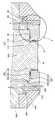
도 1은 종래의 건식식각공정에 사용되는 플라즈마 처리설비를 보여주는 단면도이다.1 is a cross-sectional view showing a plasma processing apparatus used in a conventional dry etching process.
도 1을 참조하면, 종래의 플라즈마 식각설비는 챔버와, 상기 챔버의 내부에 설치되며, 막질이 상부에 형성된 웨이퍼가 안착되며, 하부전극을 갖는 정전척과, 상기 정전척의 상부에 위치되도록 상기 챔버에 설치되는 상부전극과, 상기 챔버의 내부에 반응성 가스를 공급하는 가스공급부를 갖는다.Referring to FIG. 1, a conventional plasma etching apparatus is provided in a chamber, an electrostatic chuck having a film formed thereon, and having a film quality disposed thereon, an electrostatic chuck having a lower electrode, and positioned above the electrostatic chuck. It has an upper electrode installed, and a gas supply unit for supplying a reactive gas into the chamber.
따라서, 상기 챔버는 그 내부에 상기 가스공급부로부터 반응성 가스가 공급되고, 상기 상부 및 하부전극에 외부의 전원으로부터 RF전원이 가해지면, 그 내부에는 플라즈마 분위기가 형성된다.Therefore, when the reactive gas is supplied from the gas supply part to the chamber, and the RF power is applied to the upper and lower electrodes from an external power source, a plasma atmosphere is formed therein.
특히, 종래의 플라즈마 처리설비의 정전척의 외측부에는 포커스링이 구비된다. 상기 포커스링은 Si 재질로 이루어지고, 상기 정전척의 외측부를 에워싼다. 따라서, 상기 포커스링은 상기 정전척에 안착된 웨이퍼 상에 플라즈마의 발생 영역이 균일하게 형성되도록 한다.In particular, the focus ring is provided on the outer side of the electrostatic chuck of the conventional plasma processing equipment. The focus ring is made of Si material and surrounds an outer portion of the electrostatic chuck. Thus, the focus ring allows the generation area of the plasma to be uniformly formed on the wafer seated on the electrostatic chuck.
한편, 상기 포커스링의 주변에는 다수개의 링들이 더 설치된다. 이를 좀 더 상세하게 설명하도록 한다.Meanwhile, a plurality of rings are further installed around the focus ring. This will be explained in more detail.
도 1에 도시된 바와 같이, 정전척(20)은 그 외측둘레에 단차부를 갖는다. 상기 포커스링(30)은 상기 단차부에 설치된다. 상기 포커스링(30)의 외측부에는 다수개의 링들이 배치된다. 상기 다수개의 링들은 상기 정전척(20)의 외측둘레에 배치 되되, 상기 포커스링(30)의 저면부에 배치되는 홀더링(50)과, 상기 홀더링(50)의 외측부에 배치되는 아우터 링과, 상기 아우터 링의 상부에 배치되되, 상기 포커스링의 외측부를 감싸는 커버링으로 구성된다.As shown in Fig. 1, the
여기서, 상기 홀더링(50)과 상기 포커스링(30)의 외주면의 사이와 링들의 사이 공간에는 화살표를 따르는 유로가 형성되는 갭이 형성된다. 상기 갭은 챔버의 내부에서의 공정 진행 이후의 가스가 배기되는 배기유로이다.Here, a gap is formed in the space between the
이에 더하여, 상기 플라즈마 처리설비 중에, TEL사의 Me_SCCM 설비는 상기 포커스링(30)의 열전도율을 향상시키도록 상기 정전척(20)과 상기 포커스링(30)의 사이에 개재되는 Si 재질의 러버(31)를 갖는다.In addition, among the plasma processing equipment, TEL's Me_SCCM facility is made of
상기 러버(31)는 도 1에 도시된 바와 같이, 상기 포커스링(30)의 저면과 정전척(20)의 단차부에 개재된다.As shown in FIG. 1, the
이와 같은 구성을 갖는 종래의 플라즈마 처리설비의 작용을 설명하도록 한다.The operation of the conventional plasma processing equipment having such a configuration will be described.
도 1을 참조하면, 도면에 도시되지는 않았지만, 외부전원은 상/하부전극으로 RF전원을 인가한다. 가스공급부는 반응성 가스를 챔버의 내부로 공급한다. 따라서, 상기 챔버의 내부에 공급된 반응성 가스는 챔버의 내부에서 플라즈마로 형성된다. 상기 플라즈마의 반응 이온들은 웨이퍼의 자기 바이어스 전위에 의하여 웨이퍼(W)로 당겨지고, 상기 당겨지는 반응 이온들은 상기 웨이퍼(W) 상에 형성된 막질을 식각한다.Referring to FIG. 1, although not shown in the drawing, an external power source applies RF power to upper and lower electrodes. The gas supply part supplies the reactive gas into the chamber. Thus, the reactive gas supplied inside the chamber is formed into a plasma inside the chamber. Reaction ions of the plasma are attracted to the wafer W by the self bias potential of the wafer, and the pulled reaction ions etch a film formed on the wafer W.
이때, 상기 반응 이온들은 서로 접하고 있는 포커스링(30)의 내주면과 정전 척(20)의 외주면을 식각하여, 상기 포커스링(30)의 내주면과 상기 정전척(20)의 외주면의 사이에 틈(B)을 발생시킨다. 따라서, 종래에는 상기 틈(B)으로 유입되는 반응 이온들은 도 1에 도시된 화살표 방향을 따르는 유로를 따라 유입되어, 정전척(20)의 단차부에 설치된 러버(31)를 버닝시키는 문제점이 있다.In this case, the reaction ions etch the inner circumferential surface of the
또한, 식각된 이후의 반응 이온들은 상기 화살표를 따르는 유로를 경유하여 챔버의 외부로 배기된다. 이때, 종래에는 고온이 형성된 상기 반응 이후의 반응 이온들은 상기와 같이 러버(31)를 버닝시키는 문제점이 있다.In addition, the reaction ions after etching are exhausted to the outside of the chamber via the flow path following the arrow. At this time, conventionally, the reaction ions after the reaction in which the high temperature is formed have a problem of burning the
이에 더하여, 종래에는 상기 반응 이온들에 의하여 웨이퍼(W)의 막질이 식각될 때에 발생되는 폴리머(P) 또는 부산물이 상기 틈(B)에 쌓이거나, 상기 화살표를 따르는 유로의 내부로 유입되어 쌓이는 문제점도 있다.In addition, conventionally, polymer P or by-products generated when the film quality of the wafer W is etched by the reaction ions are accumulated in the gap B or flows into the passage along the arrow. There is also a problem.
따라서, 본 발명은 상기와 같은 문제점을 해결할 수 있도록 안출된 것으로서, 본 발명의 제 1목적은 정전척과 포커스링과의 사이에 개재되는 실링부재의 버닝을 방지할 수 있는 갭 발생방지구조 및 이를 갖는 플라즈마 처리설비를 제공함에 있다.Accordingly, the present invention has been made to solve the above problems, the first object of the present invention is to prevent the burning of the sealing member interposed between the electrostatic chuck and the focus ring and having a gap generating structure To provide a plasma processing equipment.
본 발명의 제 2목적은 정전척과 포커스링과의 사이에 형성되는 공간에 식각후의 폴리머 또는 부산물이 쌓이는 것을 방지할 수 있는 갭 발생방지구조 및 이를 갖는 플라즈마 처리설비를 제공함에 있다.A second object of the present invention is to provide a gap preventing structure and a plasma processing apparatus having the same, which can prevent the polymer or by-products from being accumulated in the space formed between the electrostatic chuck and the focus ring.
본 발명은 전술한 목적을 달성하기 위하여 갭발생방지구조를 제공한다.The present invention provides a gap preventing structure to achieve the above object.
상기 갭 발생방지구조는 척과, 상기 척의 외측부에 배치되는 링과, 상기 척과 상기 링과의 사이 공간을 외부로부터 격리시키는 갭방지부를 포함한다.The gap preventing structure includes a chuck, a ring disposed on an outer side of the chuck, and a gap preventing portion that separates a space between the chuck and the ring from the outside.
여기서, 상기 척은 그 외측둘레에 제 1단차면과 제 2단차면으로 이루어진 단차부가 형성되고, 상기 링은 상기 단차부에 배치되고, 상기 척과 상기 링과의 사이 공간은 상기 링의 내주면과 상기 제 1단차면과의 사이에 형성되는 제 1공간과, 상기 링의 저면과 상기 제 2단차면과의 사이에 형성되는 제 2공간을 갖는 것이 바람직하다.Here, the chuck is formed in the stepped portion consisting of a first step surface and the second step surface, the ring is disposed in the step portion, the space between the chuck and the ring is the inner peripheral surface of the ring and the It is preferable to have a 1st space formed between a 1st step surface, and a 2nd space formed between the bottom face of the said ring and a said 2nd step surface.
또한, 상기 갭방지부는 상기 척의 제 1외면과 밀착되도록 상기 링으로부터 일정 길이 연장되어 상기 제 1공간을 외부로부터 밀폐하는 제 1연장부와, 상기 척의 제 2외면과 밀착되도록 상기 링으로부터 일정 길이 연장되어 상기 제 2공간을 외부로부터 밀폐하는 제 2연장부를 갖는 것이 바람직하다.The gap preventing part extends a predetermined length from the ring to be in close contact with the first outer surface of the chuck and extends a predetermined length from the ring to be in close contact with the second outer surface of the chuck. It is preferable to have a 2nd extension part which seals the said 2nd space from the exterior.
또한, 상기 척의 제 1외면은 상기 제 1연장부가 끼워져 결합되는 제 1결합홈이고, 상기 척의 제 2외면은 상기 제 2연장부가 끼워져 결합되는 제 2결합홈일 수도 있다.In addition, the first outer surface of the chuck may be a first coupling groove into which the first extension part is fitted and coupled, and the second outer surface of the chuck may be a second coupling groove into which the second extension portion is fitted and coupled.
한편, 상기 갭방지부는 상기 링의 제 1외면과 밀착되도록 상기 척으로부터 일정 길이 연장되어 상기 제 1공간을 외부로부터 밀폐하는 제 1'연장부와, 상기 링의 제 2외면과 밀착되도록 상기 척으로부터 일정 길이 연장되어 상기 제 2공간을 외부로부터 밀폐하는 제 2'연장부를 가질 수도 있다.On the other hand, the gap preventing portion extends a predetermined length from the chuck to be in close contact with the first outer surface of the ring and the first 'extension to seal the first space from the outside, and from the chuck to be in close contact with the second outer surface of the ring It may have a second 'extending portion extending a predetermined length to seal the second space from the outside.
여기서, 상기 링의 제 1외면은 상기 제 1'연장부가 끼워져 결합되는 제 1'결합홈이고, 상기 링의 제 2 면은 상기 제 2연장부가 끼워져 결합되는 제 2'결합홈일 수도 있다.Here, the first outer surface of the ring may be a first 'coupling groove to which the first' extension part is fitted and coupled, and the second surface of the ring may be a second 'coupling groove to which the second extension portion is fitted and coupled.
또 한편, 상기 척과 상기 링과의 사이 공간에는 실링부재가 개재되는 것이 바람직하다.On the other hand, it is preferable that a sealing member is interposed in the space between the chuck and the ring.
여기서, 상기 실링부재는 상기 링의 내주면과 상기 링의 저면 각각에 형성되는 제 1홈에 끼워져 배치되는 것이 바람직하다.Here, the sealing member is preferably disposed in the first groove formed in each of the inner peripheral surface of the ring and the bottom surface of the ring.
또한, 상기 실링부재는 상기 척의 제 1단차면과 상기 척의 제 2단차면 각각에 형성되는 제 2홈에 끼워져 배치될 수도 있다.In addition, the sealing member may be inserted into a second groove formed in each of the first step surface of the chuck and the second step surface of the chuck.
본 발명은 전술한 목적을 달성하기 위하여 갭발생방지구조를 갖는 플라즈마 처리설비를 제공한다.The present invention provides a plasma processing apparatus having a gap preventing structure in order to achieve the above object.
상기 플라즈마 처리설비는 그 내부에 플라즈마 분위기가 형성되는 챔버와, 상기 챔버의 상단에 설치되는 상부전극과, 상기 챔버의 하단에 설치되며 하부전극을 갖고 그 상면에 웨이퍼가 안착되는 정전척과, 상기 정전척의 외측부에 배치되는 링과, 상기 척과 상기 링과의 사이 공간을 외부로부터 격리시키는 갭방지부를 포함한다.The plasma processing apparatus includes a chamber in which a plasma atmosphere is formed therein, an upper electrode installed at an upper end of the chamber, an electrostatic chuck installed at a lower end of the chamber, and having a lower electrode mounted thereon, and a wafer mounted on an upper surface thereof, A ring disposed at an outer side of the chuck, and a gap preventing portion that isolates a space between the chuck and the ring from the outside.
여기서, 상기 정전척은 그 외측둘레에 제 1단차면과 제 2단차면으로 이루어진 단차부를 갖고, 상기 링은 상기 단차부에 배치되고, 상기 정전척과 상기 링과의 사이 공간은 상기 링의 내주면과 상기 제 1단차면과의 사이에 형성되는 제 1공간과, 상기 링의 저면과 상기 제 2단차면과의 사이에 형성되는 제 2공간을 갖는 것이 바람직하다.Here, the electrostatic chuck has a stepped portion comprising a first stepped surface and a second stepped surface on an outer circumference thereof, the ring is disposed in the stepped portion, and a space between the electrostatic chuck and the ring is formed with an inner circumferential surface of the ring. It is preferable to have a 1st space formed between the said 1st step surface, and a 2nd space formed between the bottom face of the said ring and a said 2nd step surface.
여기서, 상기 링은 그 외측부가 상기 정전척의 외경보다 큰 외경을 갖으며 상기 단차부에 배치되는 포커스링인 것이 바람직하다.Here, the ring is preferably a focus ring whose outer portion has an outer diameter larger than that of the electrostatic chuck and is disposed on the stepped portion.
그리고, 상기 정전척의 외측부에는 상기 포커스링의 저부에 위치되는 홀더링을 더 구비하는 것이 바람직하다.In addition, the outer side of the electrostatic chuck is preferably provided with a holder ring located at the bottom of the focus ring.
또한, 상기 갭방지부는 상기 정전척의 제 1외면과 밀착되도록 상기 링으로부터 일정 길이 연장되어 상기 제 1공간을 외부로부터 밀폐하는 제 1연장부와, 상기 정전척의 제 2외면과 밀착되도록 상기 링으로부터 일정 길이 연장되어 상기 제 2공간을 외부로부터 밀폐하는 제 2연장부를 갖는 것이 바람직하다.The gap preventing part may extend from the ring to be in close contact with the first outer surface of the electrostatic chuck, and may be fixed to the first outer part to seal the first space from the outside, and to be in contact with the second outer surface of the electrostatic chuck. It is preferred to have a second extension that extends in length to seal the second space from the outside.
또한, 상기 갭방지부는 상기 홀더링의 상면과 상기 정전척의 제 3면과 밀착되도록 상기 포커스링의 저부로부터 일정 길이 연장되어 상기 제 2공간을 외부로부터 밀폐하는 제 3연장부를 갖을 수도 있다.The gap preventing part may have a third extension part which extends a predetermined length from the bottom of the focus ring to be in close contact with the upper surface of the holder ring and the third surface of the electrostatic chuck to seal the second space from the outside.
이에 더하여, 상기 정전척의 제 1외면은 상기 제 1연장부가 끼워져 결합되는 제 1결합홈이고, 상기 정전척의 제 2외면은 상기 제 2연장부가 끼워져 결합되는 제 2결합홈일 수 있다.In addition, the first outer surface of the electrostatic chuck may be a first coupling groove into which the first extension part is fitted and coupled, and the second outer surface of the electrostatic chuck may be a second coupling groove into which the second extension portion is fitted.
한편, 상기 갭방지부는 상기 링의 제 1외면과 밀착되도록 상기 정전척으로부터 일정 길이 연장되어 상기 제 1공간을 외부로부터 밀폐하는 제 1'연장부와, 상기 링의 제 2외면과 밀착되도록 상기 정전척으로부터 일정 길이 연장되어 상기 제 2공간을 외부로부터 밀폐하는 제 2'연장부를 갖을 수도 있다.Meanwhile, the gap preventing part extends a predetermined length from the electrostatic chuck so as to be in close contact with the first outer surface of the ring and closes the first space from the outside, and the electrostatic force is in close contact with the second outer surface of the ring. It may have a second 'extension extending from the chuck a certain length to seal the second space from the outside.
여기서, 상기 갭방지부는 상기 포커스링의 저면과 상기 정전척의 제 3면과 밀착되도록 상기 홀더링의 상단으로부터 일정 길이 연장되어 상기 제 2공간을 외부 로부터 밀폐하는 제 3'연장부를 가질 수도 있다.Here, the gap preventing part may have a third 'extension part which extends a predetermined length from an upper end of the holder ring to be in close contact with the bottom surface of the focus ring and the third surface of the electrostatic chuck to seal the second space from the outside.
또한, 상기 링의 제 1외면은 상기 제 1'연장부가 끼워져 결합되는 제 1'결합홈이고, 상기 링의 제 2외면은 상기 제 2연장부가 끼워져 결합되는 제 2'결합홈일 수 있다.In addition, the first outer surface of the ring may be a first 'combination groove into which the first' extension part is fitted and coupled, and the second outer surface of the ring may be a second 'coupling groove into which the second extension part is fitted and coupled.
그리고, 상기 정전척과 상기 링과의 사이 공간에는 실링부재가 개재되는 것이 바람직하다.The sealing member may be interposed between the electrostatic chuck and the ring.
여기서, 상기 실링부재는 상기 링의 내주면과 상기 링의 저면 각각에 형성되는 제 1홈에 끼워져 배치될 수 있다.Here, the sealing member may be inserted into the first groove formed in each of the inner peripheral surface of the ring and the bottom surface of the ring.
또한, 상기 실링부재는 상기 척의 제 1단차면과 상기 척의 제 2단차면 각각에 형성되는 제 2홈에 끼워져 배치될 수도 있다.In addition, the sealing member may be inserted into a second groove formed in each of the first step surface of the chuck and the second step surface of the chuck.
이하, 첨부되는 도면들을 참조로 하여, 본 발명의 갭 발생방지구조 및 이를 갖는 플라즈마 처리설비를 설명하도록 한다.Hereinafter, with reference to the accompanying drawings, it will be described the gap generating structure and the plasma processing apparatus having the same of the present invention.
도 2는 본 발명의 갭 발생방지구조를 갖는 플라즈마 처리설비를 보여주는 단면도이다.2 is a cross-sectional view showing a plasma processing apparatus having a gap preventing structure of the present invention.
도 2를 참조하면, 본 발명의 갭 발생방지구조를 갖는 플라즈마 처리설비는 그 내부에 플라즈마 분위기가 형성되는 챔버(100)를 구비한다. 상기 챔버(100)는 그 내부에 상부전극(110)과 정전척(200)을 구비한다. 상기 상부전극(110)은 상기 챔버(100)의 내부 상단에 설치된다. 상기 정전척(200)은 그 내부에 하부전극(120)과 외부로부터 전원을 인가받아 일정 온도로 가열되는 히터(130)를 구비한다. 막질 이 형성된 웨이퍼(W)는 상기 정전척(200)의 상면에 안착된다.Referring to FIG. 2, a plasma processing apparatus having a gap preventing structure of the present invention includes a
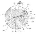
그리고, 도 3을 참조하면, 상기 정전척(200)은 그 외측부에 배치되는 포커스링(300)을 구비한다. 상기 포커스링(300)은 상기 정전척(200)의 외측둘레에 형성된 단차부(210)에 배치된다.3, the
도 4를 참조하면, 상기 정전척(200)의 단차부(210)는 상기 포커스링(300)의 내주면(301)을 마주보는 제 1단차면(211)과, 상기 제 1단차면(211)과 수직을 이루고 상기 포커스링(300)의 저면(302)을 마주보는 제 2단차면(212)을 갖는다. 상기 제 1단차면(211)과 상기 제 2단차면(212)은 서로 수직을 이룬다.Referring to FIG. 4, the stepped
따라서, 상기 포커스링(300)의 내주면(301)은 상기 제 1단차면(211)과 마주보도록 위치되고, 그 저면(302)은 상기 제 2단차면(212)과 마주보도록 위치된다. 이때, 상기 포커스링(300)의 내주면(301)과 상기 정전척(200)의 제 1단차면(211)의 사이에는 제 1공간(S1)이 형성된다. 상기 포커스링(300)의 저면(302)과 상기 정전척(200)의 제 2단차면(212)의 사이에는 제 2공간(S2)이 형성된다.Thus, the inner
여기서, 도 3에 도시된 바와 같이, 상기 포커스링(300)의 최외곽의 외경은 상기 정전척(200)의 최외곽의 외경보다 큰 외경을 갖는다. 따라서, 상기 포커스링(300)의 외측부는 상기 정전척(200)의 외측둘레로부터 돌출된다.3, the outer diameter of the outermost portion of the
다음, 본 발명에 따르는 갭방지부(400)를 설명하도록 한다.Next, to explain the
도 3을 참조로 하면, 상기 갭방지부(400)는 상기 정전척(200)의 제 1단차면(211)과 밀착되도록 상기 포커스링(300)의 내주면(301)으로부터 일정 길이 돌출된 제 1연장부(410)와, 상기 정전척(200)의 제 2단차면(212)과 밀착되도록 상기 포 커스링(300)의 저면(302)으로부터 일정 길이로 돌출된 제 2연장부(420)를 갖는다. 따라서, 상기 제 1연장부(410)와 상기 제 2연장부(420)는 제 1공간(S1)과 제 2공간(S2)을 외부로부터 밀폐시킬 수 있다.Referring to FIG. 3, the
또한, 도 4를 참조하면, 상기 정전척(200)은 상기 제 1연장부(410)가 끼워지는 제 1결합홈(211a)과 상기 제 2연장부(420)가 끼워지는 제 2결합홈(212a)을 가질 수 있다. 상기 제 1결합홈(211a)은 상기 정전척(200)의 제 1단차면(211)의 상단에 형성되고, 상기 제 2결합홈(212a)은 상기 정전척(200)의 제 2단차면(212)에 형성된다.In addition, referring to FIG. 4, the
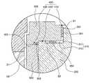
한편, 도 6을 참조로 하면, 본 발명에 따르는 갭방지부(400)는 상기 포커스링(300)의 내주면(301)에 밀착되도록 상기 정전척(200)의 제 1단차면(211)으로부터 일정 길이 돌출된 제 1'연장부(410')와, 상기 포커스링(300)의 저면(302)에 밀착되도록 상기 정전척(200)의 제 2단차면(212)으로부터 일정 길이로 돌출된 제 2'연장부(420')를 가질 수도 있다. 따라서, 상기 제 1'연장부(410')와 상기 제 2'연장부(420')는 제 1공간(S1)과 제 2공간(S2)을 외부로부터 밀폐시킬 수 있는 구조이다.Meanwhile, referring to FIG. 6, the
도 7을 참조하면, 상기 포커스링(300)은 상기 제 1'연장부(410')가 끼워지는 제 1'결합홈(311a)과 상기 제 2'연장부(420')가 끼워지는 제 2'결합홈(312a)을 가질 수도 있다. 상기 제 1'결합홈(311a)은 상기 포커스링(300)의 내주면(301)의 상단에 형성되고, 상기 제 2'결합홈(312a)은 상기 포커스링(300)의 저면(302)에 형성될 수 있다.Referring to FIG. 7, the
또 한편, 도 4 및 도 7에 도시된 바와 같이, 포커스링(300)과 정전척(200)의 사이 공간, 즉 제 1공간(S1)과 제 2공간(S2)에는 제 1,2실링부재(351,352)가 각각 개재될 수 있다. 또한, 상기 실링부재는 도 5 및 도 8에 도시된 바와 같이 오링 타잎의 제 1',2'실링부재(351',352')일 수도 있다. 상기 실링부재들(351,352,351',352')은 러버로 이루어질 수도 있고 금속으로 이루어질 수도 있다.4 and 7, the first and second sealing members are disposed in the space between the
먼저, 도 5를 참조하면, 포커스링(300)은 상기 실링부재들(351,352)이 각각 끼워지는 홈을 갖는다. 상기 홈은 제 1홈(301a)과 제 2홈(302a)을 갖는다. 상기 제 1홈(301a)은 상기 포커스링(300)의 내주면(301)에 형성되고, 상기 제 2홈(302a)은 상기 포커스링(300)의 저면(302)에 형성될 수 있다.First, referring to FIG. 5, the
또한, 도 8을 참조하면, 정전척(200)은 상기 실링부재들(351',352')이 각각 끼워지는 홈을 갖는다. 상기 홈은 제 1'홈(201a)과 제 2'홈(202a)을 갖는다. 상기 제 1'홈(201a)은 상기 정전척(200)의 제 1단차면(211)에 형성되고, 상기 제 2'홈(202a)은 상기 정전척(200)의 제 2단차면(212)에 형성될 수 있다.In addition, referring to FIG. 8, the
또 한편, 도 2에 도시된 포커스링(300)의 저부에는 홀더링(500)이 더 배치된다. 상기 홀더링(500)의 내주면은 상기 정전척(200)의 외주면과 밀착될 수 있다.In addition, a
그리고, 상기 포커스링(300)은 그 저면(302)으로부터 일정길이 연장되어 상기 홀더링(500)의 상면에 밀착되는 제 3연장부(430)를 구비할 수 있다. 따라서, 본 발명에 따르는 갭방지부(400)는 상기 제 3연장부(430)를 더 구비할 수 있다. 그리고, 제 2공간(S2)은 상기 제 3연장부(430)와 상기 홀더링(500)의 상면이 서로 밀착 되기 때문에 외부로부터 밀폐될 수 있다.In addition, the
한편, 도 3에 도시된 바와 같이, 홀더링(500)의 외측부에는 쿼츠로 이루어진 아우터 링(530)이 배치된다. 상기 아우터 링(530)의 내주면과 상기 홀더링(500)의 외주면의 사이에는 일정 간격의 제 1갭(G1)이 형성될 수 있다.Meanwhile, as illustrated in FIG. 3, an
그리고, 상기 아우터 링(530)의 상단에는 상기 포커스링(300)의 외측부를 감싸는 이너 커버링(510)이 배치된다. 상기 아우터 링(530)의 내주면과 상기 포커스링(300)의 외주면의 사이에는 일정 간격의 제 2갭(G2)이 형성된다.In addition, an
상기 제 1갭(G1)과 상기 제 2갭(G2)은 서로 연결되는 유로일 수 있다. 상기 유로는 상기 포커스링(300)의 외부 즉, 챔버(100)의 내부공간에 노출될 수 있다. 상기 유로는 상기 챔버(100)의 내부공간에 잔존될 수 있는 반응이후의 이온들이 챔버(100)의 외부로 배기되는 배기유로일 수 있다.The first gap G1 and the second gap G2 may be flow paths connected to each other. The flow path may be exposed to the outside of the
이에 더하여, 상기 아우터 링(530)의 상단부에는 상기 이너 커버링(510)의 외측부를 감싸는 아우터 커버링(520)이 배치된다. 여기서, 상기 이너 커버링(510)의 외주면과 상기 아우터 링(530)의 상단면은 상기 아우터 커버링(520)의 내면과 서로 밀착될 수 있다.In addition, an
다음은, 상기와 같은 구성을 갖는 본 발명의 갭 발생방지구조를 갖는 플라즈마 처리설비에 대한 작용 및 효과를 설명하도록 한다.Next, the operation and effects of the plasma processing apparatus having the gap generating structure of the present invention having the above-described configuration will be described.
도 2를 참조하면, 도시되지 않은 가스공급부는 플라즈마 반응 가스를 일정량으로 챔버(100)의 내부로 공급한다. 이와 아울러, 외부의 전원공급부는 상부전 극(110)과 하부전극(120)으로 RF전원을 인가한다. 그리고, 정전척(200)의 내부에 내설된 히터(130)는 외부로부터 전원을 인가받아 일정 온도로 가열된다. 따라서, 상기 챔버(100)의 내부에는 플라즈마 분위기가 형성됨과 아울러 일정 온도로 가열된다.Referring to FIG. 2, the gas supply unit (not shown) supplies the plasma reaction gas into the
이때, 상기 챔버(100)의 내부에 형성된 반응 이온들은 웨이퍼(W)상에 형성된 막질을 식각한다. 여기서, 포커스링(300)은 정전척(200)의 외측부에 배치되어, 상기 반응 이온들을 웨이퍼(W)의 상면으로 이동될 수 있도록 가이드할 수 있다.At this time, the reaction ions formed in the
또한, 상기와 같이 웨이퍼(W)의 막질이 식각된 이후에 상기 챔버(100)의 내부에는 폴리머 및 부산물이 생성된다. 이와 같은 폴리머 및 부산물은 아우터 커버링(520)의 외측부로 유동되어 챔버(100)의 외부로 배기될 수 있다.In addition, after the film quality of the wafer W is etched as described above, polymers and by-products are generated in the
여기서, 도 3에 도시된 바와 같이, 본 발명에 따르는 포커스링(300)은 그 내주면(301)과 저면(302)에 일정 길이로 돌출된 제 1,2연장부(410,420)를 구비하고, 상기 제 1,2연장부(410,420)는 상기 정전척(200)의 제 1단차면(211)과 제 2단차면(212)의 표면에 밀착된다, 따라서, 웨이퍼(W) 상으로 이동되는 반응이온들은 제 1,2공간(S1, S2)으로 유입되지 않을 수 있다.As shown in FIG. 3, the
좀 더 상세하게는, 포커스링(300)의 상단부와 정전척(200)의 상단부에 배치되는 제 1연장부(410)가 제 1공간(S1)을 외부로부터 밀폐한다. 따라서, 상기 반응 이온들이 제 1공간(S1)으로 유입되는 것을 방지할 뿐만 아니라, 포커스링(300)의 상단부가 반응 이온들에 의하여 일부 식각됨에 의하여 발생되는 폴리머가 제 1공간(S1)으로 유입되어 증착되는 것을 방지할 수도 있다.More specifically, the
또한, 상기 제 1공간(S1)에는 제 1실링부재(351)가 개재되기 때문에 상기 제 1공간(S1)으로 미량의 상기 반응 이온들과 폴리머가 유입된다 할 지라도, 상기 유입된 반응이온들과 폴리머가 제 2공간(S2)으로 유동되는 것을 방지 할 수 있다.In addition, since the
또한, 도 5에 도시된 바와 같이, 상기 제 1'실링부재(351')는 포커스링(300)의 내주면(301)에 형성된 제 1홈(301a)에 끼워져 고정되기 때문에, 상기 포커스링(300)의 내주면(301)과 정전척(200)의 제 1단차면(211)의 사이에서의 실링 포인트(sealing point)의 위치가변은 최소화 될 수 있다.In addition, as shown in FIG. 5, since the first 'sealing member 351' is inserted into and fixed to the
그리고, 포커스링(300)의 저면(302)에 형성된 제 2연장부(420)는 정전척의 제 2단차면(212)과 밀착되기 때문에, 제 2공간(S2)을 외부로부터 밀폐한다. 따라서, 상기 반응 이온들이 홀더링(500)과 제 3연장부(430)와의 접촉공간을 통하여 제 2공간(S2)으로 유입되는 것을 방지할 수 있다.Since the
또한, 상기 제 1공간(S2)에는 제 2실링부재(352)가 개재되기 때문에 상기 제 2공간(S2)으로 미량의 상기 반응 이온들과 폴리머가 유입된다 할 지라도, 상기 유입된 반응이온들과 폴리머가 제 1공간(S1)으로 유동되는 것을 방지 할 수 있다.In addition, since the
또한, 도 5에 도시된 바와 같이, 상기 제 2'실링부재(352')는 포커스링(300)의 저면(302)에 형성된 제 2홈(302a)에 끼워져 고정되기 때문에, 상기 포커스링(300)의 저면(301)과 정전척(200)의 제 2단차면(212)의 사이에서의 실링 포인트(sealing point)의 위치가변은 최소화 될 수 있다.In addition, as shown in FIG. 5, since the second 'sealing member 352' is fitted into and fixed to the
이에 더하여, 도 2에 도시된 바와 같이, 포커스링(300)의 저면(301)에 형성된 제 3연장부(430)는 홀더링(500)의 상단부와 밀착된다. 또한, 상기 제 3연장 부(430)의 내측과 상기 홀더링(500)의 상단에는 러버 또는 금속재질로 이루어진 제 3실링부재(453)가 더 개재된다.In addition, as shown in FIG. 2, the
따라서, 챔버(100)의 내부에서 생성되고, 배기유로를 통하여 배기되는 폴리머 및 부산물은 상기 제 3연장부(430)와 상기 제 3실링부재(453)로 인하여 포커스링(300)의 저면(302)과 홀더링(500)의 상단의 사이가 밀폐되기 때문에 제 2공간(S2)으로 유입되지 않을 수 있다.Therefore, the polymer and by-products generated inside the
이상에서 설명한 바와 같이, 본 발명에 따르는 갭방지부(400)는 3곳의 실링 포인트를 갖는다. 즉, 제 1실링 포인트는 제 1공간(S1)에 위치되는 제 1실링부재(351)의 설치위치이며, 제 2실링 포인트는 제 2공간(S2)에 위치되는 제 2실링부재(352)의 설치위치이며, 제 3실링 포인트는 포커스링(300)의 제 3연장부(430)와 홀더링(500)의 상단의 사이에 개재되는 제 3실링부재(353)의 설치위치이다.As described above, the
이상, 상기에서는 포커스링(300)에 형성된 제 1,2,3연장부(410,420,430)가 정전척(200)의 제 1단차면(211)과 제 2단차면(212)과, 홀더링(500)의 상단면과 각각 밀착되어, 제 1,2공간(S1,S2)이 외부로부터 밀폐되는 작용과, 3곳의 실링 포인트 즉, 제 1실링부재(351)와 제 2실링부재(352)와 제 3실링부재(353)가 마련되는 위치에서의 실링포인트 위치가변이 최소화되는 작용에 대하여 설명하였다.In the above description, the first, second and
그러나, 본 발명에 따르는 갭 방지부(400)의 제 1,2연장부(410,420)는 도 2 내지 도 5에 도시된 바와 같이 포커스링(300)에 형성될 수도 있지만, 정전척(200)에 형성될 수도 있다. 이에 대한 구체적인 실시예를 도 6 내지 도 8을 참조로 하여 설명하도록 한다.However, although the first and
도 6을 참조로 하면, 정전척(200)의 제 1단차면(211)으로부터 일정 길이로 돌출된 제 1'연장부(410')는 단차부(210)에 배치된 포커스링(300)의 내주면(301)에 밀착될 수 있다. 따라서, 상기 포커스링(300)의 외부에서 형성된 반응 이온 및 폴리머는 제 1공간(S1)으로 용이하게 유입되지 않는다.Referring to FIG. 6, the first 'extension 410' protruding from the first stepped
또한, 상기 정전척(200)의 제 2단차면(212)으로부터 일정 길이로 돌출된 제 2'연장부(420')는 단차부(210)에 배치된 포커스링(300)의 저면(302)에 밀착될 수 있다. 따라서, 배기유로를 통하여 배기되는 폴리머는 제 2공간(S2)으로 용이하게 유입되지 않을 수 있다.In addition, the second 'extension 420' protruding from the
도 7을 참조하면, 상기 정전척(200)에 형성된 제 1'연장부(410')는 포커스링(300)의 내주면에 형성된 제 1'결합홈(311a)에 끼워진다. 또한, 상기 정전척(200)의 제 2'연장부(420')는 포커스링(300)의 저면(302)에 형성된 제 2'결합홈(312a)에 끼워진다. 따라서, 제 1',2'결합홈(311a,312a)에 상기 제 1',2'연장부(410',420')가 끼워짐으로써, 제 1,2공간(S1,S2)은 외부로부터 용이하게 밀폐될 수 있다.Referring to FIG. 7, the first '
이에 더하여, 포커스링(300)은 정전척(200)의 외측부에 배치되어 정전척(200)의 상면을 기준으로 측방 또는 상하방으로 쉽게 유동되지 않을 수 있다.In addition, the
도 7을 참조하면, 정전척(200)의 제 1단차면(211)과 포커스링(300)의 내주면(301)의 사이에는 제 1실링부재(351)가 개재된다. 또한, 도 8을 참조하면, 제 1'실링부재(351')는 정전척(200)의 제 1단차면(211)에 형성된 제 1'홈(201a)에 끼워진다. 따라서, 챔버(100)의 내부에 형성된 반응 이온들은 제 1'연장부(410')에 의 하여 제 1공간(S1)으로 유입됨이 방지되지만, 미량의 반응 이온들이 제 1공간(S1)으로 유입되는 경우에, 상기 유입된 반응 이온들은 상기 제 1,1'실링부재(351,351')에 의하여 제 2공간(S2)으로 유동됨이 방지될 수 있다. 그리고, 제 1'실링부재(351')가 상기 제 1'홈(201a)에 끼워지기 때문에 제 1'실링부재(351')의 위치는 용이하게 고정될 수 있다.Referring to FIG. 7, a
또한, 도 7을 참조하면, 상기 정전척(200)의 제 2단차면(212)과 포커스링(300)의 저면(302)의 사이에는 제 2실링부재(352)가 개재된다. 또한, 도 8에 도시된 바와 같이, 제 2'실링부재(352')는 정전척(200)의 제 2단차면(212)에 형성된 제 2'홈(202a)에 끼워진다. 따라서, 배기유로를 통하여 배기되는 폴리머는 제 2'연장부(420')에 의하여 제 2공간(S2)으로 유입됨이 방지되지만, 미량의 폴리머 제 2공간으로 유입되는 경우에, 상기 유입된 폴리머는 상기 제 2,2'실링부재(352,352')에 의하여 제 1공간(S1)으로 유동됨이 방지될 수 있다. 그리고, 제 2'실링부재(352')가 상기 제 2'홈(202a)에 끼워지기 때문에 제 2'실링부재(352')의 위치는 용이하게 고정될 수 있다.In addition, referring to FIG. 7, a
또한, 배기유로를 통하여 배기되는 폴리머는 포커스링(300)의 저면(302)으로부터 일정 길이 연장되고 홀더링(500)의 상단과 밀착되는 제 3연장부(430)에 의하여 제 2공간(S2)으로 유입됨이 방지될 수도 있다. 이에 더하여, 상기 폴리머는 상기 제 3연장부(430)의 내측에 위치되고 홀더링(500)의 상단에 배치되는 제 3실링부재(353)에 의하여 제 2공간(S2)으로 유입됨이 더 용이하게 방지될 수도 있다.In addition, the polymer exhausted through the exhaust passage extends a predetermined length from the
한편, 도 3 및 도 6에 도시된 제 3연장부(430)는 도면에 도시되지는 않았지 만, 홀더링(500)의 상단부가 상방으로 일정길이로 연장되어 포커스링(300)의 저면(302)과 밀착되는 제 3'연장부일 수도 있다. 따라서, 상기 제 3'연장부가 상기 포커스링(300)의 저면(302)에 밀착되고, 제 3실링부재(353)가 제 3'연장부의 내측에 위치되도록 상기 홀더링(500)의 상단에 개재되기 때문에, 배기유로를 통하여 배기되는 폴리머는 제 2공간(S2)으로 유입되지 않을 수 있다.Meanwhile, although not illustrated in the drawing, the
이상에서 설명한 바와 같이, 본 발명은 정전척과 포커스링과의 사이에 개재되는 실링부재의 버닝을 방지할 수 있는 효과를 갖는다.As described above, the present invention has the effect of preventing the burning of the sealing member interposed between the electrostatic chuck and the focus ring.
또한, 본 발명은 정전척과 포커스링과의 사이에 형성되는 공간에 다중의 실링 포인트를 형성함으로써, 챔버의 내부에서 형성되는 반응이온들과 폴리머등이 상기 공간에 침투되어 증착되는 것을 용이하게 방지할 수 있는 효과를 갖는다.In addition, the present invention by forming a plurality of sealing points in the space formed between the electrostatic chuck and the focus ring, it is possible to easily prevent the reaction ions and polymers formed in the interior of the chamber to penetrate and deposit the space. Has the effect.
또한, 본 발명은 정전척 또는 포커스링에 형성되는 연장부들을 정전척 또는 포커스링에 형성되는 결합홈들에 끼워져 고정되도록 함으로써, 정전척에서의 포커스링의 틀어짐을 방지할 수 있는 효과도 있다.In addition, the present invention also has the effect of preventing the twist of the focus ring in the electrostatic chuck by fixing the extension portion formed in the electrostatic chuck or focus ring is fitted into the coupling grooves formed in the electrostatic chuck or focus ring.
Claims (19)
Translated fromKoreanPriority Applications (5)
| Application Number | Priority Date | Filing Date | Title |
|---|---|---|---|
| KR1020070002959AKR100849179B1 (en) | 2007-01-10 | 2007-01-10 | Structure for protecting gap formation and plasma processing equipment having the same |
| DE102008004289ADE102008004289A1 (en) | 2007-01-10 | 2008-01-07 | Gap formation prevention structure for use in wafer processing unit, has holder for holding wafer and gap prevention unit with ring, which is positioned on outer side of holder |
| US11/971,568US7727354B2 (en) | 2007-01-10 | 2008-01-09 | Structure for preventing gap formation and plasma processing equipment having the same |
| JP2008002005AJP2008172240A (en) | 2007-01-10 | 2008-01-09 | Gap generation prevention structure and plasma processing apparatus having the same |
| CNA2008101092448ACN101286469A (en) | 2007-01-10 | 2008-01-10 | Structure for preventing void formation and plasma processing apparatus |
Applications Claiming Priority (1)
| Application Number | Priority Date | Filing Date | Title |
|---|---|---|---|
| KR1020070002959AKR100849179B1 (en) | 2007-01-10 | 2007-01-10 | Structure for protecting gap formation and plasma processing equipment having the same |
Publications (2)
| Publication Number | Publication Date |
|---|---|
| KR20080065828A KR20080065828A (en) | 2008-07-15 |
| KR100849179B1true KR100849179B1 (en) | 2008-07-30 |
Family
ID=39646204
Family Applications (1)
| Application Number | Title | Priority Date | Filing Date |
|---|---|---|---|
| KR1020070002959AExpired - Fee RelatedKR100849179B1 (en) | 2007-01-10 | 2007-01-10 | Structure for protecting gap formation and plasma processing equipment having the same |
Country Status (5)
| Country | Link |
|---|---|
| US (1) | US7727354B2 (en) |
| JP (1) | JP2008172240A (en) |
| KR (1) | KR100849179B1 (en) |
| CN (1) | CN101286469A (en) |
| DE (1) | DE102008004289A1 (en) |
Cited By (4)
| Publication number | Priority date | Publication date | Assignee | Title |
|---|---|---|---|---|
| KR101146906B1 (en) | 2004-07-06 | 2012-05-22 | 주성엔지니어링(주) | Electrode static chuck |
| CN106548959A (en)* | 2015-09-23 | 2017-03-29 | 北京北方微电子基地设备工艺研究中心有限责任公司 | Reaction chamber and semiconductor processing equipment |
| KR20230150403A (en)* | 2017-07-24 | 2023-10-30 | 램 리써치 코포레이션 | Moveable edge ring designs |
| US12444579B2 (en) | 2020-03-23 | 2025-10-14 | Lam Research Corporation | Mid-ring erosion compensation in substrate processing systems |
Families Citing this family (29)
| Publication number | Priority date | Publication date | Assignee | Title |
|---|---|---|---|---|
| TWI246873B (en)* | 2001-07-10 | 2006-01-01 | Tokyo Electron Ltd | Plasma processing device |
| US20090221150A1 (en)* | 2008-02-29 | 2009-09-03 | Applied Materials, Inc. | Etch rate and critical dimension uniformity by selection of focus ring material |
| WO2010021890A2 (en)* | 2008-08-19 | 2010-02-25 | Lam Research Corporation | Edge rings for electrostatic chucks |
| US8869741B2 (en)* | 2008-12-19 | 2014-10-28 | Lam Research Corporation | Methods and apparatus for dual confinement and ultra-high pressure in an adjustable gap plasma chamber |
| US8707705B2 (en)* | 2009-09-03 | 2014-04-29 | General Electric Company | Impingement cooled transition piece aft frame |
| US8270141B2 (en)* | 2009-11-20 | 2012-09-18 | Applied Materials, Inc. | Electrostatic chuck with reduced arcing |
| US20120318455A1 (en)* | 2011-06-14 | 2012-12-20 | Andreas Fischer | Passive compensation for temperature-dependent wafer gap changes in plasma processing systems |
| CN103094166B (en)* | 2011-10-31 | 2015-04-15 | 北京北方微电子基地设备工艺研究中心有限责任公司 | Wafer carrying device and semiconductor processing equipment comprising the same |
| KR20130086806A (en)* | 2012-01-26 | 2013-08-05 | 삼성전자주식회사 | Thin film deposition apparatus |
| US10755902B2 (en)* | 2015-05-27 | 2020-08-25 | Tokyo Electron Limited | Plasma processing apparatus and focus ring |
| JP6435247B2 (en)* | 2015-09-03 | 2018-12-05 | 新光電気工業株式会社 | Electrostatic chuck device and method of manufacturing electrostatic chuck device |
| CN116110846A (en)* | 2016-01-26 | 2023-05-12 | 应用材料公司 | Wafer edge ring lift solution |
| DE102016206193A1 (en)* | 2016-04-13 | 2017-10-19 | Trumpf Gmbh + Co. Kg | Electro-adhesive gripper with fractal electrodes |
| US9966292B2 (en)* | 2016-07-12 | 2018-05-08 | Globalfoundries Inc. | Centering fixture for electrostatic chuck system |
| US10504765B2 (en) | 2017-04-24 | 2019-12-10 | Applied Materials, Inc. | Electrostatic chuck assembly having a dielectric filler |
| JP6839624B2 (en)* | 2017-07-19 | 2021-03-10 | 東京エレクトロン株式会社 | Processing device of the object to be processed and inspection method of the processing device |
| WO2019088204A1 (en)* | 2017-11-06 | 2019-05-09 | 日本碍子株式会社 | Electrostatic chuck assembly, electrostatic chuck, and focus ring |
| TWI780093B (en)* | 2017-12-15 | 2022-10-11 | 美商蘭姆研究公司 | Ring structures and systems for use in a plasma chamber |
| JP7055040B2 (en)* | 2018-03-07 | 2022-04-15 | 東京エレクトロン株式会社 | Placement device and processing device for the object to be processed |
| KR102096985B1 (en)* | 2018-08-23 | 2020-04-03 | 세메스 주식회사 | Substrate processing apparatus |
| JP7039688B2 (en)* | 2019-02-08 | 2022-03-22 | 株式会社日立ハイテク | Plasma processing equipment |
| JP7340938B2 (en)* | 2019-02-25 | 2023-09-08 | 東京エレクトロン株式会社 | Mounting table and substrate processing equipment |
| JP7333712B2 (en)* | 2019-06-05 | 2023-08-25 | 東京エレクトロン株式会社 | Electrostatic chuck, support table and plasma processing equipment |
| JP7361002B2 (en)* | 2019-10-02 | 2023-10-13 | 東京エレクトロン株式会社 | plasma processing equipment |
| JP2021068782A (en)* | 2019-10-21 | 2021-04-30 | 東京エレクトロン株式会社 | Placing platform assembly, substrate processing device, and sealing member |
| JP7308767B2 (en)* | 2020-01-08 | 2023-07-14 | 東京エレクトロン株式会社 | Mounting table and plasma processing device |
| JP7446176B2 (en)* | 2020-07-31 | 2024-03-08 | 東京エレクトロン株式会社 | Mounting table and plasma processing equipment |
| KR102751528B1 (en)* | 2020-09-01 | 2025-01-07 | 삼성전자주식회사 | Plasma processing equipment |
| KR102833573B1 (en)* | 2023-07-28 | 2025-07-14 | 피에스케이홀딩스 (주) | Apparatus for treating substrate |
Citations (4)
| Publication number | Priority date | Publication date | Assignee | Title |
|---|---|---|---|---|
| JP2002033376A (en)* | 2000-07-17 | 2002-01-31 | Tokyo Electron Ltd | Placing device of body to be treated |
| JP2003152063A (en) | 2001-11-09 | 2003-05-23 | Applied Materials Inc | Electrostatic chuck and semiconductor manufacturing device |
| KR20060029359A (en)* | 2004-10-01 | 2006-04-06 | 삼성전자주식회사 | Semiconductor dry etching equipment |
| KR20070008980A (en)* | 2005-07-14 | 2007-01-18 | 삼성전자주식회사 | Chuck Assembly of Semiconductor Etching Equipment and Semiconductor Etching Equipment |
Family Cites Families (7)
| Publication number | Priority date | Publication date | Assignee | Title |
|---|---|---|---|---|
| US6074488A (en)* | 1997-09-16 | 2000-06-13 | Applied Materials, Inc | Plasma chamber support having an electrically coupled collar ring |
| KR20000011778U (en) | 1998-12-08 | 2000-07-05 | 윤종용 | Electrostatic chuck insulation ring of dry etching device |
| JP4592916B2 (en)* | 2000-04-25 | 2010-12-08 | 東京エレクトロン株式会社 | Placement device for workpiece |
| US6554954B2 (en)* | 2001-04-03 | 2003-04-29 | Applied Materials Inc. | Conductive collar surrounding semiconductor workpiece in plasma chamber |
| US7582186B2 (en)* | 2002-12-20 | 2009-09-01 | Tokyo Electron Limited | Method and apparatus for an improved focus ring in a plasma processing system |
| KR20050091854A (en) | 2004-03-11 | 2005-09-15 | 삼성전자주식회사 | Focus ring of semiconductor wafer manufacturing device |
| KR20060005740A (en) | 2004-07-14 | 2006-01-18 | 삼성전자주식회사 | Internal Process Chamber of Dry Etching Equipment |
- 2007
- 2007-01-10KRKR1020070002959Apatent/KR100849179B1/ennot_activeExpired - Fee Related
- 2008
- 2008-01-07DEDE102008004289Apatent/DE102008004289A1/ennot_activeWithdrawn
- 2008-01-09USUS11/971,568patent/US7727354B2/ennot_activeExpired - Fee Related
- 2008-01-09JPJP2008002005Apatent/JP2008172240A/enactivePending
- 2008-01-10CNCNA2008101092448Apatent/CN101286469A/enactivePending
Patent Citations (4)
| Publication number | Priority date | Publication date | Assignee | Title |
|---|---|---|---|---|
| JP2002033376A (en)* | 2000-07-17 | 2002-01-31 | Tokyo Electron Ltd | Placing device of body to be treated |
| JP2003152063A (en) | 2001-11-09 | 2003-05-23 | Applied Materials Inc | Electrostatic chuck and semiconductor manufacturing device |
| KR20060029359A (en)* | 2004-10-01 | 2006-04-06 | 삼성전자주식회사 | Semiconductor dry etching equipment |
| KR20070008980A (en)* | 2005-07-14 | 2007-01-18 | 삼성전자주식회사 | Chuck Assembly of Semiconductor Etching Equipment and Semiconductor Etching Equipment |
Cited By (8)
| Publication number | Priority date | Publication date | Assignee | Title |
|---|---|---|---|---|
| KR101146906B1 (en) | 2004-07-06 | 2012-05-22 | 주성엔지니어링(주) | Electrode static chuck |
| CN106548959A (en)* | 2015-09-23 | 2017-03-29 | 北京北方微电子基地设备工艺研究中心有限责任公司 | Reaction chamber and semiconductor processing equipment |
| CN106548959B (en)* | 2015-09-23 | 2020-01-03 | 北京北方华创微电子装备有限公司 | Reaction chamber and semiconductor processing equipment |
| KR20230150403A (en)* | 2017-07-24 | 2023-10-30 | 램 리써치 코포레이션 | Moveable edge ring designs |
| KR20240042567A (en)* | 2017-07-24 | 2024-04-02 | 램 리써치 코포레이션 | Moveable edge ring designs |
| KR102720332B1 (en) | 2017-07-24 | 2024-10-21 | 램 리써치 코포레이션 | Moveable edge ring designs |
| KR102725131B1 (en) | 2017-07-24 | 2024-10-31 | 램 리써치 코포레이션 | Moveable edge ring designs |
| US12444579B2 (en) | 2020-03-23 | 2025-10-14 | Lam Research Corporation | Mid-ring erosion compensation in substrate processing systems |
Also Published As
| Publication number | Publication date |
|---|---|
| CN101286469A (en) | 2008-10-15 |
| US20090044751A1 (en) | 2009-02-19 |
| US7727354B2 (en) | 2010-06-01 |
| JP2008172240A (en) | 2008-07-24 |
| KR20080065828A (en) | 2008-07-15 |
| DE102008004289A1 (en) | 2008-08-28 |
Similar Documents
| Publication | Publication Date | Title |
|---|---|---|
| KR100849179B1 (en) | Structure for protecting gap formation and plasma processing equipment having the same | |
| CN110890263B (en) | Dry cleaning apparatus and dry cleaning method | |
| US11367610B2 (en) | Film forming and process container cleaning method | |
| TWI479564B (en) | Semiconductor manufacturing apparatus and semiconductor manufacturing method | |
| KR102806341B1 (en) | Focus ring and plasma processing apparatus including the same | |
| JP2013512564A (en) | Electrostatic chuck with inclined side walls | |
| US8845816B2 (en) | Method extending the service interval of a gas distribution plate | |
| KR102773631B1 (en) | Low resistance restraint liners for use in plasma chambers | |
| US20070258075A1 (en) | Apparatus for processing a semiconductor wafer and method of forming the same | |
| US8992689B2 (en) | Method for removing halogen-containing residues from substrate | |
| TW202343548A (en) | Contact formation process for cmos devices | |
| KR20210068972A (en) | Focus Ring and plasma device including the same | |
| KR20070013118A (en) | Plasma etching device | |
| KR20050004995A (en) | Apparatus for processing a substrate using a plasma | |
| KR20070054766A (en) | Substrate processing equipment | |
| US20150017811A1 (en) | Method for processing base body to be processed | |
| KR100783060B1 (en) | Focus ring and substrate processing apparatus having the same | |
| US7732009B2 (en) | Method of cleaning reaction chamber, method of forming protection film and protection wafer | |
| KR100669111B1 (en) | Chamber Assembly and Substrate Processing Apparatus Having the Same | |
| TWI892179B (en) | Plasma processing apparatus | |
| KR100689810B1 (en) | Baffle of Etching Device for Semiconductor Device Manufacturing | |
| KR20040094240A (en) | Semicounductor manufacture equipment having improving focus ring | |
| CN119008373A (en) | Stray plasma prevention apparatus for substrate processing chamber | |
| KR100604826B1 (en) | Plasma processing apparatus for processing wafer edges and plasma processing method thereof | |
| JP2007042979A (en) | Manufacturing method of semiconductor device |
Legal Events
| Date | Code | Title | Description |
|---|---|---|---|
| A201 | Request for examination | ||
| PA0109 | Patent application | St.27 status event code:A-0-1-A10-A12-nap-PA0109 | |
| PA0201 | Request for examination | St.27 status event code:A-1-2-D10-D11-exm-PA0201 | |
| D13-X000 | Search requested | St.27 status event code:A-1-2-D10-D13-srh-X000 | |
| D14-X000 | Search report completed | St.27 status event code:A-1-2-D10-D14-srh-X000 | |
| E902 | Notification of reason for refusal | ||
| PE0902 | Notice of grounds for rejection | St.27 status event code:A-1-2-D10-D21-exm-PE0902 | |
| E13-X000 | Pre-grant limitation requested | St.27 status event code:A-2-3-E10-E13-lim-X000 | |
| P11-X000 | Amendment of application requested | St.27 status event code:A-2-2-P10-P11-nap-X000 | |
| P13-X000 | Application amended | St.27 status event code:A-2-2-P10-P13-nap-X000 | |
| E701 | Decision to grant or registration of patent right | ||
| PE0701 | Decision of registration | St.27 status event code:A-1-2-D10-D22-exm-PE0701 | |
| PG1501 | Laying open of application | St.27 status event code:A-1-1-Q10-Q12-nap-PG1501 | |
| GRNT | Written decision to grant | ||
| PR0701 | Registration of establishment | St.27 status event code:A-2-4-F10-F11-exm-PR0701 | |
| PR1002 | Payment of registration fee | St.27 status event code:A-2-2-U10-U11-oth-PR1002 Fee payment year number:1 | |
| PG1601 | Publication of registration | St.27 status event code:A-4-4-Q10-Q13-nap-PG1601 | |
| PR1001 | Payment of annual fee | St.27 status event code:A-4-4-U10-U11-oth-PR1001 Fee payment year number:4 | |
| R18-X000 | Changes to party contact information recorded | St.27 status event code:A-5-5-R10-R18-oth-X000 | |
| FPAY | Annual fee payment | Payment date:20120706 Year of fee payment:5 | |
| PR1001 | Payment of annual fee | St.27 status event code:A-4-4-U10-U11-oth-PR1001 Fee payment year number:5 | |
| LAPS | Lapse due to unpaid annual fee | ||
| PC1903 | Unpaid annual fee | St.27 status event code:A-4-4-U10-U13-oth-PC1903 Not in force date:20130724 Payment event data comment text:Termination Category : DEFAULT_OF_REGISTRATION_FEE | |
| PC1903 | Unpaid annual fee | St.27 status event code:N-4-6-H10-H13-oth-PC1903 Ip right cessation event data comment text:Termination Category : DEFAULT_OF_REGISTRATION_FEE Not in force date:20130724 |