KR100846276B1 - Liquid crystal display device - Google Patents
Liquid crystal display deviceDownload PDFInfo
- Publication number
- KR100846276B1 KR100846276B1KR1020020051514AKR20020051514AKR100846276B1KR 100846276 B1KR100846276 B1KR 100846276B1KR 1020020051514 AKR1020020051514 AKR 1020020051514AKR 20020051514 AKR20020051514 AKR 20020051514AKR 100846276 B1KR100846276 B1KR 100846276B1
- Authority
- KR
- South Korea
- Prior art keywords
- liquid crystal
- substrate
- insulating film
- pixel electrode
- pixel
- Prior art date
- Legal status (The legal status is an assumption and is not a legal conclusion. Google has not performed a legal analysis and makes no representation as to the accuracy of the status listed.)
- Expired - Fee Related
Links
Images


Classifications
- G—PHYSICS
- G09—EDUCATION; CRYPTOGRAPHY; DISPLAY; ADVERTISING; SEALS
- G09G—ARRANGEMENTS OR CIRCUITS FOR CONTROL OF INDICATING DEVICES USING STATIC MEANS TO PRESENT VARIABLE INFORMATION
- G09G3/00—Control arrangements or circuits, of interest only in connection with visual indicators other than cathode-ray tubes
- G09G3/20—Control arrangements or circuits, of interest only in connection with visual indicators other than cathode-ray tubes for presentation of an assembly of a number of characters, e.g. a page, by composing the assembly by combination of individual elements arranged in a matrix no fixed position being assigned to or needed to be assigned to the individual characters or partial characters
- G09G3/2007—Display of intermediate tones
- G09G3/2011—Display of intermediate tones by amplitude modulation
- G—PHYSICS
- G02—OPTICS
- G02F—OPTICAL DEVICES OR ARRANGEMENTS FOR THE CONTROL OF LIGHT BY MODIFICATION OF THE OPTICAL PROPERTIES OF THE MEDIA OF THE ELEMENTS INVOLVED THEREIN; NON-LINEAR OPTICS; FREQUENCY-CHANGING OF LIGHT; OPTICAL LOGIC ELEMENTS; OPTICAL ANALOGUE/DIGITAL CONVERTERS
- G02F1/00—Devices or arrangements for the control of the intensity, colour, phase, polarisation or direction of light arriving from an independent light source, e.g. switching, gating or modulating; Non-linear optics
- G02F1/01—Devices or arrangements for the control of the intensity, colour, phase, polarisation or direction of light arriving from an independent light source, e.g. switching, gating or modulating; Non-linear optics for the control of the intensity, phase, polarisation or colour
- G02F1/13—Devices or arrangements for the control of the intensity, colour, phase, polarisation or direction of light arriving from an independent light source, e.g. switching, gating or modulating; Non-linear optics for the control of the intensity, phase, polarisation or colour based on liquid crystals, e.g. single liquid crystal display cells
- G02F1/133—Constructional arrangements; Operation of liquid crystal cells; Circuit arrangements
- G02F1/1333—Constructional arrangements; Manufacturing methods
- G02F1/1343—Electrodes
- G02F1/134309—Electrodes characterised by their geometrical arrangement
- G02F1/134363—Electrodes characterised by their geometrical arrangement for applying an electric field parallel to the substrate, i.e. in-plane switching [IPS]
- G—PHYSICS
- G09—EDUCATION; CRYPTOGRAPHY; DISPLAY; ADVERTISING; SEALS
- G09G—ARRANGEMENTS OR CIRCUITS FOR CONTROL OF INDICATING DEVICES USING STATIC MEANS TO PRESENT VARIABLE INFORMATION
- G09G3/00—Control arrangements or circuits, of interest only in connection with visual indicators other than cathode-ray tubes
- G09G3/20—Control arrangements or circuits, of interest only in connection with visual indicators other than cathode-ray tubes for presentation of an assembly of a number of characters, e.g. a page, by composing the assembly by combination of individual elements arranged in a matrix no fixed position being assigned to or needed to be assigned to the individual characters or partial characters
- G09G3/34—Control arrangements or circuits, of interest only in connection with visual indicators other than cathode-ray tubes for presentation of an assembly of a number of characters, e.g. a page, by composing the assembly by combination of individual elements arranged in a matrix no fixed position being assigned to or needed to be assigned to the individual characters or partial characters by control of light from an independent source
- G09G3/36—Control arrangements or circuits, of interest only in connection with visual indicators other than cathode-ray tubes for presentation of an assembly of a number of characters, e.g. a page, by composing the assembly by combination of individual elements arranged in a matrix no fixed position being assigned to or needed to be assigned to the individual characters or partial characters by control of light from an independent source using liquid crystals
- G09G3/3611—Control of matrices with row and column drivers
- G09G3/3648—Control of matrices with row and column drivers using an active matrix
- G09G3/3659—Control of matrices with row and column drivers using an active matrix the addressing of the pixel involving the control of two or more scan electrodes or two or more data electrodes, e.g. pixel voltage dependant on signal of two data electrodes
- G—PHYSICS
- G02—OPTICS
- G02F—OPTICAL DEVICES OR ARRANGEMENTS FOR THE CONTROL OF LIGHT BY MODIFICATION OF THE OPTICAL PROPERTIES OF THE MEDIA OF THE ELEMENTS INVOLVED THEREIN; NON-LINEAR OPTICS; FREQUENCY-CHANGING OF LIGHT; OPTICAL LOGIC ELEMENTS; OPTICAL ANALOGUE/DIGITAL CONVERTERS
- G02F1/00—Devices or arrangements for the control of the intensity, colour, phase, polarisation or direction of light arriving from an independent light source, e.g. switching, gating or modulating; Non-linear optics
- G02F1/01—Devices or arrangements for the control of the intensity, colour, phase, polarisation or direction of light arriving from an independent light source, e.g. switching, gating or modulating; Non-linear optics for the control of the intensity, phase, polarisation or colour
- G02F1/13—Devices or arrangements for the control of the intensity, colour, phase, polarisation or direction of light arriving from an independent light source, e.g. switching, gating or modulating; Non-linear optics for the control of the intensity, phase, polarisation or colour based on liquid crystals, e.g. single liquid crystal display cells
- G02F1/133—Constructional arrangements; Operation of liquid crystal cells; Circuit arrangements
- G02F1/1333—Constructional arrangements; Manufacturing methods
- G02F1/1337—Surface-induced orientation of the liquid crystal molecules, e.g. by alignment layers
- G02F1/133776—Surface-induced orientation of the liquid crystal molecules, e.g. by alignment layers having structures locally influencing the alignment, e.g. unevenness
- G—PHYSICS
- G09—EDUCATION; CRYPTOGRAPHY; DISPLAY; ADVERTISING; SEALS
- G09G—ARRANGEMENTS OR CIRCUITS FOR CONTROL OF INDICATING DEVICES USING STATIC MEANS TO PRESENT VARIABLE INFORMATION
- G09G2300/00—Aspects of the constitution of display devices
- G09G2300/04—Structural and physical details of display devices
- G09G2300/0421—Structural details of the set of electrodes
- G09G2300/0434—Flat panel display in which a field is applied parallel to the display plane
- G—PHYSICS
- G09—EDUCATION; CRYPTOGRAPHY; DISPLAY; ADVERTISING; SEALS
- G09G—ARRANGEMENTS OR CIRCUITS FOR CONTROL OF INDICATING DEVICES USING STATIC MEANS TO PRESENT VARIABLE INFORMATION
- G09G2310/00—Command of the display device
- G09G2310/02—Addressing, scanning or driving the display screen or processing steps related thereto
- G09G2310/0243—Details of the generation of driving signals
- G09G2310/0251—Precharge or discharge of pixel before applying new pixel voltage
- G—PHYSICS
- G09—EDUCATION; CRYPTOGRAPHY; DISPLAY; ADVERTISING; SEALS
- G09G—ARRANGEMENTS OR CIRCUITS FOR CONTROL OF INDICATING DEVICES USING STATIC MEANS TO PRESENT VARIABLE INFORMATION
- G09G2310/00—Command of the display device
- G09G2310/06—Details of flat display driving waveforms
- G09G2310/061—Details of flat display driving waveforms for resetting or blanking
- G—PHYSICS
- G09—EDUCATION; CRYPTOGRAPHY; DISPLAY; ADVERTISING; SEALS
- G09G—ARRANGEMENTS OR CIRCUITS FOR CONTROL OF INDICATING DEVICES USING STATIC MEANS TO PRESENT VARIABLE INFORMATION
- G09G2320/00—Control of display operating conditions
- G09G2320/02—Improving the quality of display appearance
- G09G2320/028—Improving the quality of display appearance by changing the viewing angle properties, e.g. widening the viewing angle, adapting the viewing angle to the view direction
Landscapes
- Physics & Mathematics (AREA)
- Engineering & Computer Science (AREA)
- General Physics & Mathematics (AREA)
- Chemical & Material Sciences (AREA)
- Crystallography & Structural Chemistry (AREA)
- Theoretical Computer Science (AREA)
- Nonlinear Science (AREA)
- Computer Hardware Design (AREA)
- Optics & Photonics (AREA)
- Mathematical Physics (AREA)
- Liquid Crystal (AREA)
- Geometry (AREA)
- Control Of Indicators Other Than Cathode Ray Tubes (AREA)
- Liquid Crystal Display Device Control (AREA)
Abstract
Translated fromKoreanDescription
Translated fromKorean도 1은 본 발명에 따른 실시 형태 1의 액정 표시 장치에 있어서의 화소 근방의 회로배치 패턴 구성을 설명하는 도면.BRIEF DESCRIPTION OF THE DRAWINGS The figure explaining the circuit arrangement pattern structure of the pixel vicinity in the liquid crystal display device of
도 2는 종래 및 본 발명의 액정 표시 장치의 회로 구성을 설명하는 도면.2 is a diagram illustrating a circuit configuration of a liquid crystal display device of the related art and the present invention.
도 3은 종래의 액정 표시 장치에 있어서의 화소 근방의 회로배치 패턴 구성을 설명하는 도면.3 is a diagram illustrating a circuit arrangement pattern configuration near a pixel in a conventional liquid crystal display device.
도 4는 종래의 액정 표시 장치에 있어서의 화소 근방의 단면을 설명하는 도면.4 is a diagram illustrating a cross section near a pixel in a conventional liquid crystal display device.
도 5는 본 발명에 따른 실시 형태 1의 액정 표시 장치에 있어서의 화소 근방의 단면을 설명하는 도면.FIG. 5 is a view for explaining a section in the vicinity of a pixel in the liquid crystal display device of
도 6은 액정층이 요철을 가지는 것에 의한 고속화의 원리를 설명하는 도면.FIG. 6 is a view for explaining the principle of speeding-up by the liquid crystal layer having irregularities. FIG.
도 7은 액정층이 요철을 가지는 것에 의한 고속화의 효과를 설명하는 도면.FIG. 7 is a diagram for explaining the effect of speedup due to the unevenness of the liquid crystal layer. FIG.
도 8은 본 발명에 따른 실시 형태 2의 액정 표시 장치에 있어서의 화소 근방의 회로배치 패턴 구성을 설명하는 도면.FIG. 8 is a diagram illustrating a circuit arrangement pattern configuration near a pixel in the liquid crystal display device of
도 9는 본 발명에 따른 실시 형태 2의 액정 표시 장치에 있어서의 화소 근방의 단면을 설명하는 도면.FIG. 9 is a view for explaining a section near a pixel in the liquid crystal display of
도 10은 본 발명에 따른 실시 형태 3의 액정 표시 장치에 있어서의 화소 근 방의 회로배치 패턴 구성을 설명하는 도면.Fig. 10 is a diagram explaining a circuit arrangement pattern configuration near a pixel in the liquid crystal display device of
도 11은 본 발명에 따른 실시 형태 3의 액정 표시 장치에 있어서의 화소 근방의 단면을 설명하는 도면.FIG. 11 is a view for explaining a section in the vicinity of a pixel in the liquid crystal display of
도 12는 본 발명에 따른 실시 형태 4의 액정 표시 장치에 있어서의 화소 근방의 회로배치 패턴 구성을 설명하는 도면.FIG. 12 is a diagram illustrating a circuit arrangement pattern configuration near a pixel in the liquid crystal display of
도 13은 본 발명에 따른 실시 형태 4의 액정 표시 장치에 있어서의 화소 근방의 단면을 설명하는 도면.FIG. 13 is a view for explaining a section in the vicinity of a pixel in the liquid crystal display device of
도 14는 본 발명에 따른 실시 형태 5 내지 실시 형태 7의 액정 표시 장치에 있어서의 화소 근방의 회로배치 패턴 구성을 설명하는 도면.FIG. 14 is a diagram illustrating a circuit arrangement pattern configuration near a pixel in the liquid crystal display device of Embodiments 5-7 according to the present invention. FIG.
도 15는 본 발명에 따른 실시 형태 5의 액정 표시 장치에 있어서의 화소 근방의 회로배치 패턴 구성을 설명하는 도면.FIG. 15 is a diagram illustrating a circuit arrangement pattern configuration near a pixel in the liquid crystal display of
도 16은 본 발명에 따른 실시 형태 5의 액정 표시 장치에 있어서의 화소 근방의 단면을 설명하는 도면.FIG. 16 is a view for explaining a cross section in the vicinity of a pixel in the liquid crystal display of
도 17은 본 발명에 따른 실시 형태 6의 액정 표시 장치에 있어서의 화소 근방의 회로배치 패턴 구성을 설명하는 도면.FIG. 17 is a diagram illustrating a circuit arrangement pattern configuration near a pixel in the liquid crystal display of
도 18은 본 발명에 따른 실시 형태 6의 액정 표시 장치에 있어서의 화소 근방의 단면(도 17의 A-A'단면)을 설명하는 도면.FIG. 18 is a view for explaining a cross section (A-A 'cross section in FIG. 17) in the vicinity of a pixel in the liquid crystal display device of
도 19는 본 발명에 따른 실시 형태 6의 액정 표시 장치에 있어서의 화소 근방의 단면(도 17의 B-B'단면)을 설명하는 도면.FIG. 19 is a view for explaining a cross section (B-B 'cross section in FIG. 17) in the vicinity of a pixel in the liquid crystal display device of
도 20은 본 발명에 따른 실시 형태 7의 액정 표시 장치에 있어서의 화소 근 방의 회로배치 패턴 구성을 설명하는 도면.Fig. 20 is a diagram illustrating a circuit arrangement pattern configuration near a pixel in the liquid crystal display of the seventh embodiment according to the present invention.
도 21은 본 발명에 따른 실시 형태 7의 액정 표시 장치에 있어서의 화소 근방의 단면을 설명하는 도면.Fig. 21 is a diagram explaining a cross section in the vicinity of a pixel in the liquid crystal display device of the seventh embodiment according to the present invention.
도 22는 본 발명에 따른 실시 형태 8의 액정 표시 장치에 있어서의 화소 근방의 회로배치 패턴 구성을 설명하는 도면.Fig. 22 is a diagram explaining a circuit arrangement pattern configuration near a pixel in the liquid crystal display of the eighth embodiment according to the present invention.
도 23은 본 발명에 따른 실시 형태 8의 액정 표시 장치에 있어서의 화소 근방의 단면을 설명하는 도면.Fig. 23 is a diagram illustrating a cross section in the vicinity of a pixel in the liquid crystal display device of
도 24는 본 발명에 따른 실시 형태 9의 액정 표시 장치에 있어서의 화소 근방의 회로배치 패턴 구성을 설명하는 도면.Fig. 24 is a diagram explaining a circuit arrangement pattern configuration near a pixel in the liquid crystal display device of Embodiment 9 according to the present invention.
도 25는 본 발명에 따른 실시 형태 10의 액정 표시 장치에 있어서의 화소 근방의 회로배치 패턴 구성을 설명하는 도면.Fig. 25 is a diagram explaining a circuit arrangement pattern configuration near a pixel in the liquid crystal display device of the tenth embodiment according to the present invention.
도 26은 본 발명에 따른 실시 형태 10의 액정 표시 장치에 있어서의 화소 근방의 단면을 설명하는 도면.Fig. 26 is a diagram illustrating a cross section near a pixel in the liquid crystal display of the tenth embodiment according to the present invention.
도 27은 본 발명에 따른 실시 형태 11의 액정 표시 장치에 있어서의 화소 근방의 회로배치 패턴 구성을 설명하는 도면.Fig. 27 is a diagram explaining a circuit arrangement pattern configuration near a pixel in the liquid crystal display device of the eleventh embodiment according to the present invention.
도 28은 본 발명에 따른 실시 형태 11의 액정 표시 장치에 있어서의 화소 근방의 단면을 설명하는 도면.Fig. 28 is a diagram explaining a cross section near a pixel in the liquid crystal display of the eleventh embodiment according to the present invention.
도 29는 본 발명에 따른 실시 형태 12의 액정 표시 장치에 있어서의 화소 근방의 회로배치 패턴 구성을 설명하는 도면.Fig. 29 is a diagram illustrating a circuit arrangement pattern configuration near a pixel in the liquid crystal display of the twelfth embodiment according to the present invention.
도 30은 본 발명에 따른 실시 형태 13의 액정 표시 장치에 있어서의 화소 근 방의 회로배치 패턴 구성을 설명하는 도면.Fig. 30 is a diagram illustrating a circuit arrangement pattern configuration near a pixel in the liquid crystal display device of Embodiment 13 according to the present invention.
도 31은 본 발명에 따른 실시 형태 13의 액정 표시 장치에 있어서의 화소 근방의 단면을 설명하는 도면.FIG. 31 is a view for explaining a section in the vicinity of a pixel in the liquid crystal display device of Embodiment 13 according to the present invention. FIG.
도 32는 본 발명에 따른 실시 형태 14 및 실시 형태 17의 액정 표시 장치에 있어서의 화소 근방의 회로배치 패턴 구성을 설명하는 도면.Fig. 32 is a diagram illustrating a circuit arrangement pattern configuration near a pixel in the liquid crystal display devices of the fourteenth and seventeenth embodiments according to the present invention.
도 33은 본 발명에 따른 실시 형태 14의 액정 표시 장치에 있어서의 화소 근방의 단면을 설명하는 도면.Fig. 33 is a diagram illustrating a cross section in the vicinity of a pixel in the liquid crystal display device of Embodiment 14 according to the present invention.
도 34는 본 발명에 따른 실시 형태 15의 액정 표시 장치에 있어서의 화소 근방의 회로배치 패턴 구성을 설명하는 도면.Fig. 34 is a diagram explaining a circuit arrangement pattern configuration near a pixel in the liquid crystal display device of the fifteenth embodiment according to the present invention.
도 35는 본 발명에 따른 실시 형태 15의 액정 표시 장치에 있어서의 화소 근방의 단면을 설명하는 도면.Fig. 35 is a diagram explaining a cross section in the vicinity of a pixel in the liquid crystal display device of the fifteenth embodiment according to the present invention.
도 36은 본 발명에 따른 실시 형태 16의 액정 표시 장치에 있어서의 화소 근방의 회로배치 패턴 구성을 설명하는 도면.Fig. 36 is a diagram illustrating a circuit arrangement pattern configuration near a pixel in the liquid crystal display device of the sixteenth embodiment according to the present invention.
도 37은 본 발명에 따른 실시 형태 16의 액정 표시 장치에 있어서의 화소 근방의 단면을 설명하는 도면.FIG. 37 is a view for explaining a section in the vicinity of a pixel in the liquid crystal display device of Embodiment 16 according to the present invention; FIG.
도 38은 본 발명에 따른 실시 형태 17의 액정 표시 장치에 있어서의 화소 근방의 회로배치 패턴 구성을 설명하는 도면.Fig. 38 is a diagram explaining a circuit arrangement pattern configuration near a pixel in the liquid crystal display device of the seventeenth embodiment according to the present invention.
도 39는 본 발명에 따른 실시 형태 18의 액정 표시 장치에 있어서의 각 배선 및 전극의 전위의 시간 변화와 액정에 인가되는 전압의 시간 변화를 설명하는 도면.Fig. 39 is a view explaining a time change of the potential of each wiring and the electrode and a time change of the voltage applied to the liquid crystal in the liquid crystal display device of Embodiment 18 according to the present invention.
도 40은 본 발명에 따른 실시 형태 19의 액정 표시 장치의 구성을 설명하는 도면.40 is a diagram illustrating a configuration of a liquid crystal display device of Embodiment 19 according to the present invention.
도 41은 본 발명에 따른 실시 형태 19의 액정 표시 장치에 있어서의 각 배선 및 전극의 전위의 시간 변화와 액정에 인가되는 전압의 시간 변화를 설명하는 도면.Fig. 41 is a view for explaining the time change of the potential of each wiring and the electrode and the time change of the voltage applied to the liquid crystal in the liquid crystal display device of Embodiment 19 according to the present invention.
도 42는 본 발명에 따른 비교예 2의 액정 표시 장치에 있어서의 각 배선의 전위의 시간 변화와 화소의 투과율의 시간 변화를 설명하는 도면.Fig. 42 is a diagram illustrating a time change of the potential of each wiring and a time change of the transmittance of a pixel in the liquid crystal display of Comparative Example 2 according to the present invention.
도 43은 본 발명에 따른 비교예 2와 실시 형태 21의 액정 표시 장치에 있어서의 액정의 응답특성을 설명하는 도면.Fig. 43 is a view explaining the response characteristic of liquid crystal in the liquid crystal display of Comparative Example 2 and
도 44는 응답시간의 정의를 설명하는 도면.44 illustrates a definition of a response time.
도 45는 본 발명에 따른 실시 형태 21의 액정 표시 장치에 있어서의 각 배선의 전위의 시간 변화와 화소의 투과율의 시간 변화를 설명하는 도면.Fig. 45 is a view for explaining the time change of the potential of each wiring and the time change of the transmittance of the pixel in the liquid crystal display device of
도 46은 TN 액정소자의 응답특성을 설명하는 도면.Fig. 46 is a view explaining the response characteristic of a TN liquid crystal element.
<도면의 주요 부분에 대한 부호의 설명><Explanation of symbols for the main parts of the drawings>
1, 2…기판1, 2... Board
3…평탄화 막3... Flattening membrane
4…컬러 필터4… Color filter
5…블랙 매트릭스5... Black matrix
6…편광판6... Polarizer
11…화소11... Pixel
21…전기력선21... Electric power line
22…표시부22... Display
31…신호선31... Signal line
32…주사선32... scanning line
33…제1 TFT33... First TFT
33'…제2 TFT33 '... 2nd TFT
34…액정34... LCD
35…화소 전극35... Pixel electrode
36…공통 전극36... Common electrode
36'…공통 전극 접속부36 '... Common electrode connection
36"…공통 전극배선36 "… common electrode wiring
81…절연막81... Insulating film
82…보호막82... Shield
85…배향막85... Alignment film
86…제2 절연막86... Second insulating film
101, 102, 103…선택 펄스101, 102, 103... Select pulse
110…1주기 기간110... 1 cycle period
본 발명은 신규의 구성을 가지는 액정 표시 장치에 관한 것이다.The present invention relates to a liquid crystal display device having a novel configuration.
종래의 액정 표시 장치는, 트위스티드 네마틱(TN) 표시 모드로 대표되는 바와 같이, 기판면에 대해서 거의 수직인 전계를 인가하는 표시 모드를 채용하고 있다. 그러나, TN 표시 모드에서는, 시야각 특성이 불충분하다고 하는 문제가 있다.Conventional liquid crystal display devices employ a display mode in which an electric field substantially perpendicular to the substrate surface is applied, as represented by the twisted nematic (TN) display mode. However, in the TN display mode, there is a problem that the viewing angle characteristic is insufficient.
한편, 인 플레인·스위칭(In-Plane Switching:IPS) 표시 모드가, 일본국 특허공고 소63-21907호, USP4345249호, WO91/10936호, 일본국 특허공개 평6-160878호 등의 공보에 의해 제안되어 있다.On the other hand, In-Plane Switching (IPS) display mode is disclosed by Japanese Patent Publication Nos. 63-21907, USP4345249, WO91 / 10936, and Japanese Patent Laid-Open No. 6-160878. It is proposed.
이 IPS 표시 모드에서는, 액정 구동용 전극이 액정을 협지하는 한 쌍의 기판 중 한쪽 기판 위에 형성되고, 액정에는 기판면에 대해서 평행한 성분을 가지는 전계가 인가된다. 이 IPS 표시 모드에서는, TN 표시 모드에 비해 넓은 시야각을 얻을 수 있다.In this IPS display mode, a liquid crystal drive electrode is formed on one of a pair of substrates sandwiching a liquid crystal, and an electric field having a component parallel to the substrate surface is applied to the liquid crystal. In this IPS display mode, a wider viewing angle can be obtained than in the TN display mode.
그렇지만, IPS 표시 모드에 있어서도 색조가 시각에 따라서 변화한다고 하는 문제를 가지고 있다. 이 문제를 해결하는 멀티 도메인 IPS 표시 모드가 일본국 특허공개 평9-258269 등의 공보에 의해 제안되어 있다. 이 멀티 도메인 IPS 표시 모드에 의한 액정 표시 장치를 도 2, 도 3 및 도 4를 이용해서 설명한다.However, also in the IPS display mode, there is a problem that the color tone changes with time. A multi-domain IPS display mode that solves this problem has been proposed by Japanese Patent Laid-Open No. 9-258269. The liquid crystal display device by this multi-domain IPS display mode is demonstrated using FIG. 2, FIG. 3, and FIG.
도 2는 멀티 도메인 IPS 표시 모드에 의한 액정 표시 장치의 구성을 도시하는 도면이다. 화소 전극(35)에 신호전위를 공급하는 신호 드라이버(51)와, 화소를 선택하는 전위를 공급하는 주사 드라이버(52)와, 공통 전극(36)에 전위를 공급하는 공통 전극 드라이버(54)와, 신호 드라이버(51) 및 주사 드라이버(52) 및 공통 전극 드라이버(54)를 제어하는 표시 제어 장치(53)를 가지고 있다.2 is a diagram illustrating a configuration of a liquid crystal display device in a multi-domain IPS display mode. A
기판(1)에는, 주사 드라이버(52)에 접속된 복수의 주사선(32)과, 신호 드라이버(51)에 접속되고, 또한 주사선(32)과 교차한 신호선(31)과, 주사선(32)과 신호선(31)의 교점부근에 대응해서 배치되어, 주사선(32)과 신호선(31)과 전기적으로 접속된 제1 TFT(33)와, 제1 TFT(33)에 전기적으로 접속되어, 신호선(31)에 대응한 화소 전극(35)과, 화소 전극(35)에 대응한 공통 전극(36)과, 공통 전극(36)과 공통 전극 드라이버(54)에 전기적으로 접속된 공통 전극 접속부(36')가 구비되어 있다.The
신호선(31)과 주사선(32)에 둘러싸인 영역에 대응해서 화소(11)가 형성되고, 복수의 화소(11)에 의해 표시부(22)가 형성되어 있다.The
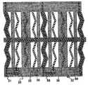
도 3은 멀티 도메인 IPS 표시 모드에 의한 액정 표시 장치의 화소 근방의 회로배치 패턴 구성을 도시하는 도면이다. 주사선(32)과 신호선(31)은 서로 교차하고, 주사선(32)과 신호선(31)에 둘러싸인 영역에 대응해서 화소(11)가 형성되어 있다. 제1 TFT(33)는 주사선(32)과 신호선(31)의 교점부근에 대응해서 배치되어, 주사선(32)과 신호선(31)과 화소 전극(35)에 전기적으로 접속되어 있다. 공통 전극(36)은 화소 전극(35)에 대응해서 배치되고, 공통 전극(36)과 화소 전극(35)으로 기판면에 대해서 평행한 성분을 가지는 전계를 발생시킨다. 화소 전극(35)과 공통 전극(36)과 신호선(31)은 하나의 화소 내에서 1회 이상 절곡되어, 멀티 도메인을 형성하고 있다. 전계 인가시의 액정의 회전방향을 서로 이웃하는 도메인끼리 반대방향으로 하여, 시야부를 넓히기 위해서이다.3 is a diagram showing a circuit arrangement pattern configuration near a pixel of a liquid crystal display device in a multi-domain IPS display mode. The
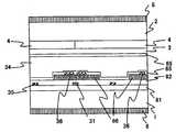
도 4는 도 3의 A-A'단면의 단면도이다. 재질이 투명 유리인 기판(1)과, 기판(1)에 대향 배치되고, 재질이 투명 유리인 기판(2)과, 기판(1)과 기판(2)으로 협 지된 액정층(34)을 가진다. 기판(1)은 공통 전극(36)과, 제1 절연막(81)을 통해 공통 전극(36)보다도 상층에 배치된 신호선(31)과, 공통 전극(36)에 대응하여, 기판(1)면에 대해서 평행한 성분을 가지는 전계를 발생시키는 화소 전극(35)과, 화소 전극(35) 위에 구비된 보호막(82)과, 보호막(82) 위에 구비된 배향막(85)과, 기판(1)의 액정에 면하지 않는 쪽의 면 위에 구비되어, 액정의 배향 상태에 따라서 광학 특성을 바꾸는 수단인 편광판(6)을 가진다.4 is a cross-sectional view taken along the line AA ′ of FIG. 3. It has the board |
기판(2)은 불필요한 간극부로부터의 광을 차광하는 차광막(5)과, 차광막(5) 위에 구비되어, R, G, B에 대응한 색을 표현하는 컬러 필터(4)와, 컬러 필터(4) 위에 구비되어, 요철을 평탄화하는 평탄화 막(3)과, 평탄화 막(3) 위에 구비된 배향막(85)과, 기판(2)의 액정에 면하지 않는 쪽의 면 위에 구비된 편광판(6)을 가진다.The
배향막(85)에는 액정을 배향시키기 위한 러빙 처리가 되어 있다. 러빙 방향은 신호선의 연신 방향(DLa)에 평행하다. 굴곡된 화소 전극의 1변과 러빙 방향이 이루는 각은 15도이고, IPS 표시 모드에 대응하고 있다. 편광판(6)의 투과축은, 각각의 편광판이 배치되어 있는 기판상의 배향막의 러빙 방향에 대해서 평행 또는 수직으로 향해져 있고, 기판(1)의 편광판과 기판(2)의 편광판은 크로스 니콜로 배치되어, 노멀리 블랙 모드에 대응하고 있다.The
화상 표시는 기판(1)면과 평행한 성분을 가지는 전계를 공통 전극(36)과 화소 전극(35)에 의해 액정(34)에 인가하여, 액정(34)을 기판(1)과 거의 평행한 면내에서 회전시키는 것에 의해 행한다.The image display applies an electric field having a component parallel to the surface of the
최근, 액정 표시 장치에의 기대는 PC(Personal Computer) 모니터에만 향한 것이 아니라, 동화에 대응한 액정 텔레비젼으로 확대되고 있다. 액정 텔레비전으로서는, 복수인으로 감상할 수 있도록 시야각이 넓은 IPS 표시 모드가 적합하다고 생각된다. 이 IPS 표시 모드에 의한 액정 표시 장치에 있어서, 보다 아름답게 동화를 표시하기 위해서는, 액정의 응답시간의 단축이 요망된다. 또, IPS 표시 모드에서는, 구동전압에 의해 색조가 변화한다고 하는 문제도 있어, 이것을 해결하는 것이 요망된다. 또한, 최근, 액정 표시 장치에 있어서, 동화상의 윤곽이 불선명해진다고 하는 문제가 지적되고 있다.In recent years, the expectation for a liquid crystal display device is not only directed to a personal computer (PC) monitor, but has been expanded to liquid crystal televisions corresponding to moving pictures. As a liquid crystal television, it is thought that the IPS display mode with a wide viewing angle is suitable for viewing by multiple people. In this liquid crystal display device in the IPS display mode, in order to display a moving picture more beautifully, it is desired to shorten the response time of the liquid crystal. In the IPS display mode, there is also a problem that the color tone changes depending on the driving voltage, and it is desired to solve this problem. Moreover, in recent years, the problem that the outline of a moving image becomes unclear in the liquid crystal display device is pointed out.
따라서, 본 발명의 제1의 목적은 신규의 화소구조에 의해 액정의 응답시간의 단축을 도모하는 것에 있다.Therefore, the first object of the present invention is to shorten the response time of the liquid crystal by the novel pixel structure.
또, 본 발명의 제2의 목적은 구동전압에 따른 색조변화가 생기지 않는 액정 표시 장치를 제공하는 것에 있다.Further, a second object of the present invention is to provide a liquid crystal display device in which color tone change does not occur according to a driving voltage.
또한, 본 발명의 제3의 목적은 동화상의 윤곽이 선명한 액정 표시 장치를 제공하는 것에 있다.Further, a third object of the present invention is to provide a liquid crystal display device having a clear outline of a moving image.
상기 목적은 이하에 나타내는 수단에 의해 달성된다.The said object is achieved by the means shown below.
본 발명의 제1 양태는, 제1 기판과, 상기 제1 기판에게 대향 배치된 제2 기판과, 상기 제1 기판과 상기 제2 기판으로 협지된 액정층과,A first aspect of the present invention is a liquid crystal layer sandwiched between a first substrate, a second substrate disposed opposite to the first substrate, the first substrate and the second substrate,
상기 제1 기판 위에 배치된 복수의 주사선과, 상기 제1 기판 위에 상기 주사선과 교차해서 배치된 신호선과, 상기 주사선과 상기 신호선에 둘러싸인 영역에 대응해서 구성되는 화소와, 상기 제1 기판 위에 배치되어, 상기 신호선에 대응한 화소 전극과, 상기 제1 기판 위에 배치되어, 상기 화소 전극에 대응한 공통 전극과, 상기 주사선과 상기 신호선의 교점에 대응해서 배치되어, 상기 신호선과 상기 주사선과 상기 화소 전극에 전기적으로 접속된 제1 액티브 소자와, 상기 제1 기판 위에 배치된 절연막을 포함하는 액정 표시 장치에 있어서,A plurality of scan lines disposed on the first substrate, a signal line disposed on the first substrate to intersect the scan line, a pixel configured to correspond to the area surrounded by the scan line and the signal line, and disposed on the first substrate And a pixel electrode corresponding to the signal line, a common electrode corresponding to the pixel electrode, and corresponding to an intersection of the scan line and the signal line, disposed on the first substrate, and corresponding to the signal line, the scan line, and the pixel electrode. A liquid crystal display device comprising: a first active element electrically connected to a; and an insulating film disposed on the first substrate;
동일한 상기 화소 내의 광 투과 영역에서, 상기 제1 기판과 상기 제2 기판 중 적어도 어느 한 쪽에, 상기 액정층의 두께를 변동시키는 요철이 설치되어 있는 것을 특징으로 한다.In the light transmitting region in the same pixel, at least one of the first substrate and the second substrate is provided with irregularities for varying the thickness of the liquid crystal layer.
본 발명의 제2 양태의 발명은, 본 발명의 제1 양태의 액정 표시 장치에 있어서,The invention of the second aspect of the present invention is the liquid crystal display device of the first aspect of the present invention.
상기 요철은 액정의 응답 속도를 단축하는 것을 목적으로 하여 의도적으로 형성된 것을 특징으로 한다. 즉, 통상의 액정 표시 장치의 제조공정에 부가해서, 요철을 형성하는 공정이 추가되어 있다.The unevenness is intentionally formed for the purpose of shortening the response speed of the liquid crystal. That is, the process of forming an unevenness | corrugation is added to the manufacturing process of a normal liquid crystal display device.
본 발명의 제3 양태는, 본 발명의 제1 양태 또는 제2 양태의 액정 표시 장치에 있어서,A third aspect of the present invention is the liquid crystal display device of the first aspect or the second aspect of the present invention,
상기 요철이 절연막에 의해 형성되어 있는 것을 특징으로 한다.The irregularities are formed by an insulating film.
본 발명의 제4 양태는, 본 발명의 제3 양태의 액정 표시 장치에 있어서,A fourth aspect of the present invention is the liquid crystal display device of the third aspect of the present invention,
상기 절연막이 상기 제1 기판 위에 형성되는 제1 절연막과, 상기 제1막 위 또한 적어도 상기 공통 전극 또는 상기 화소 전극 위에, 이것들을 절연 보호하기 위해서 형성되는 보호막과, 상기 보호막 위에 형성되는 제2 절연막을 포함하고, 상기 요철은 상기 제2 절연막에 의해 형성되는 것을 특징으로 한다.A first insulating film on which the insulating film is formed on the first substrate, a protective film formed on the first film and at least on the common electrode or the pixel electrode to insulate and protect these, and a second insulating film formed on the protective film It includes, characterized in that the irregularities are formed by the second insulating film.
본 발명의 제5 양태의 발명은, 본 발명의 제1 양태 내지 제4 양태의 액정 표시 장치에 있어서,The invention of the fifth aspect of the present invention is the liquid crystal display device of the first to fourth aspects of the present invention,
각각의 상기 화소에서, 광 투과 영역에 있어서의 상기 액정층의 오목부와 볼록부의 면적비, 및 요철의 높이의 평균치가 동등한 것을 특징으로 한다.In each of the pixels, the average value of the area ratios of the concave and convex portions of the liquid crystal layer and the height of the unevenness in the light transmitting region is equal.
본 발명의 제6 양태의 발명은, 본 발명의 제1 양태 내지 제5 양태의 액정 표시 장치에 있어서,According to a sixth aspect of the present invention, in the liquid crystal display device of the first to fifth aspects of the present invention,
상기 요철에 따른 단차가 상기 화소 전극과 상기 공통 전극의 사이에 하나만 있는 것을 특징으로 한다.There is only one step according to the unevenness between the pixel electrode and the common electrode.
본 발명의 제7 양태의 발명은, 본 발명의 제6 양태의 액정 표시 장치에 있어서,The invention of the seventh aspect of the present invention is the liquid crystal display device of the sixth aspect of the present invention.
상기 화소 전극이 상기 요철에 따른 오목부 또는 볼록부 중 어느 한쪽에 중첩되어 배치되고, 상기 공통 전극이 상기 오목부 또는 볼록부 중 상기 화소 전극이 중첩되어 있지 않은 다른 한 쪽의 부분에 중첩되어 배치되어 있는 것을 특징으로 한다.The pixel electrode is disposed to overlap one of the concave portion or convex portion according to the unevenness, and the common electrode is disposed to overlap the other portion of the concave portion or convex portion that the pixel electrode does not overlap. It is characterized by that.
본 발명의 제8 양태는, 본 발명의 제1 양태 내지 제7 양태의 액정 표시 장치에 있어서,Eighth aspect of the present invention is the liquid crystal display device of the first to seventh aspects of the present invention,
상기 요철이 상기 제1 기판 위에 형성되어 있는 것을 특징으로 한다.The unevenness is formed on the first substrate.
본 발명의 제9 양태는, 본 발명의 제8 양태의 액정 표시 장치에 있어서,A ninth aspect of the present invention is the liquid crystal display device of the eighth aspect of the present invention.
상기 화소 전극과 상기 공통 전극의 적어도 일부가, 상기 요철을 형성하고 있는 상기 절연막보다도 위에 배치되어 있는 것을 특징으로 한다.At least a part of the pixel electrode and the common electrode are disposed above the insulating film forming the unevenness.
본 발명의 제10 양태는, 본 발명의 제1 양태 내지 제7 양태의 액정 표시 장치에 있어서, 상기 요철이 상기 제2 기판 위에 형성되어 있는 것을 특징으로 한다.A tenth aspect of the present invention is the liquid crystal display device of the first to seventh aspects of the present invention, wherein the irregularities are formed on the second substrate.
본 발명의 제11 양태는, 본 발명의 제1 양태 내지 제10 양태의 액정 표시 장치에 있어서,An eleventh aspect of the present invention is the liquid crystal display device of the first to tenth aspects of the present invention,
상기 요철이 스트라이프형 또는 지그재그형으로 배치되어, 상기 요철의 연신 방향이 상기 화소 전극 또는 상기 공통 전극의 연신 방향에서 어긋나 있는 것을 특징으로 한다.The irregularities are arranged in a stripe or zigzag shape, and the extending direction of the unevenness is shifted from the extending direction of the pixel electrode or the common electrode.
본 발명의 제12 양태는, 본 발명의 제1 양태 내지 제10 양태의 액정 표시 장치에 있어서,A twelfth aspect of the present invention is the liquid crystal display device of the first to tenth aspects of the present invention,
상기 요철이 스트라이프형이고, 상기 요철에 따른 단차의 연신 방향이, 상기 액정의 초기 배향 방향과 일치하고 있는 것을 특징으로 한다.It is characterized by the above-mentioned unevenness | corrugation which is stripe type | mold, and the extending | stretching direction of the level | step difference according to the said unevenness is coincident with the initial orientation direction of the said liquid crystal.
본 발명의 제13 양태는, 본 발명의 제1 양태 내지 제12 양태의 액정 표시 장치에 있어서,A thirteenth aspect of the present invention is the liquid crystal display device of the first to twelfth aspects of the present invention,
상기 신호선과 상기 주사선과 상기 화소 전극과 상기 공통 전극 중 적어도 하나가 상기 요철에 따른 단차를 타 넘지 않고 있는 것을 것을 특징으로 한다.At least one of the signal line, the scan line, the pixel electrode, and the common electrode does not exceed the step due to the unevenness.
본 발명의 제14 양태는, 본 발명의 제1 양태 내지 제13 양태의 액정 표시 장치에 있어서,A fourteenth aspect of the present invention is the liquid crystal display device of the first to thirteenth aspects of the present invention,
상기 요철에 따른 단차의 적어도 일부가 상기 화소 전극 또는 상기 공통 전극과 중첩되어 있는 것을 특징으로 한다.At least a part of the step due to the unevenness overlaps with the pixel electrode or the common electrode.
본 발명의 제15 양태는, 본 발명의 제1 양태 내지 제14 양태의 액정 표시 장치에 있어서,A fifteenth aspect of the present invention is the liquid crystal display device of the first to fourteenth aspects of the present invention,
상기 신호선과 상기 공통 전극의 적어도 일부가, 상기 요철을 형성하고 있는 상기 절연막을 사이에 두고 중첩되어 있는 것을 특징으로 한다.At least a portion of the signal line and the common electrode overlap each other with the insulating film forming the unevenness therebetween.
본 발명의 제16 양태는, 본 발명의 제15 양태의 액정 표시 장치에 있어서,A sixteenth aspect of the present invention is the liquid crystal display device of the fifteenth aspect of the present invention.
상기 절연막이 상기 신호선과 상기 공통 전극의 중첩되어 있는 부분에서, 상기 공통 전극보다 작은 폭으로 선택적으로 형성되어 있는 것을 특징으로 한다.The insulating film is selectively formed with a width smaller than that of the common electrode in a portion where the signal line and the common electrode overlap.
본 발명의 제17 양태는, 본 발명의 제15 양태 또는 제16 양태의 액정 표시 장치에 있어서,A seventeenth aspect of the present invention is the liquid crystal display device of the fifteenth or sixteenth aspect of the present invention.
상기 액정층을 배향시키기 위한 배향막이 상기 액정층에 접해서 배치되고, 상기 신호선과 상기 절연막이 중첩되어 있는 부분에서, 상기 절연막 위에 상기 공 통 전극과 상기 배향막이 배치되어 있고, 상기 신호선의 일부분에 상기 공통 전극이 중첩되어 있는 것을 특징으로 한다. 즉, 공통 전극에 슬릿을 설치됨으로써 신호선과의 사이의 용량을 조절할 수 있다.An alignment film for aligning the liquid crystal layer is disposed in contact with the liquid crystal layer, and the common electrode and the alignment film are disposed on the insulating film at a portion where the signal line and the insulating film overlap, and a portion of the signal line is disposed. The common electrode is characterized in that the overlap. That is, the capacitance between the signal line can be adjusted by providing the slit in the common electrode.
본 발명의 제18 양태는, 본 발명의 제1 양태 내지 제17 양태의 액정 표시 장치에 있어서,An eighteenth aspect of the present invention is the liquid crystal display device of the first to seventeenth aspects of the present invention,
상기 신호선과 상기 주사선 상의 적어도 일부에 상기 요철을 형성하고 있는 상기 절연막이 배치되어 있는 것을 특징으로 한다.The said insulating film which forms the said unevenness | corrugation is arrange | positioned in the said signal line and the said scan line at least one part, It is characterized by the above-mentioned.
본 발명의 제19 양태는, 본 발명의 제4 양태 내지 제18 양태의 액정 표시 장치에 있어서,19th aspect of this invention is a liquid crystal display device of 4th-18th aspect of this invention,
상기 요철을 형성하는 상기 제2 절연막과는 별도로 상기 보호막이 상기 제1 기판 위에 요철을 가지고 배치되어, 상기 제2 절연막의 볼록부와 상기 보호막의 오목부가 중첩되어 있는 것을 특징으로 한다.In addition to the second insulating film forming the unevenness, the protective film is disposed on the first substrate with unevenness, and the convex portion of the second insulating film and the concave portion of the protective film overlap.
본 발명의 제20 양태는, 본 발명의 제1 양태 내지 제19 양태의 액정 표시 장치에 있어서,A twentieth aspect of the present invention is the liquid crystal display device of the first to nineteenth aspects of the present invention,
1화상을 표시하는 1주기 기간 중에, 상기 화소 전극의 전위와 상기 공통 전극의 전위를 동일하게 하는 수단을 가지는 것을 특징으로 한다.And a means for equalizing the potential of the pixel electrode and the potential of the common electrode during one period of displaying one image.
본 발명의 제21 양태는, 본 발명의 제20 양태의 액정 표시 장치에 있어서,21st aspect of this invention is liquid crystal display device of 20th aspect of this invention,
상기 1주기 기간 중에 상기 주사선이 2회 주사되어, 어느 한쪽의 상기 주사에 의해 상기 화소 전극에는 상기 공통 전극과 같은 전위가 공급되고, 다른 쪽의 상기 주사에 의해 화상을 표시하기 위한 전위가 상기 화소 전극에 공급되는 것을 특징으로 한다.The scanning line is scanned twice in the period of one cycle, and the same potential as that of the common electrode is supplied to the pixel electrode by either of the scanning, and the potential for displaying an image by the scanning of the other is the pixel. It is characterized in that the supply to the electrode.
본 발명의 제22 양태는, 본 발명의 제20 양태의 액정 표시 장치에 있어서,22nd aspect of this invention is liquid crystal display device of 20th aspect of this invention,
상기 제1 액티브 소자가 접속되어 있는 상기 주사선과 다른 주사선과 상기 화소 전극과 상기 공통 전극에 전기적으로 접속된 제2 액티브 소자를 가지고, 상기 1주기 기간 중에 상기 화소 전극의 전위와 상기 공통 전극의 전위를 동일하게 하는 것을 특징으로 한다.A scan line different from the scan line to which the first active element is connected, and a second active element electrically connected to the pixel electrode and the common electrode, wherein the potential of the pixel electrode and the potential of the common electrode are in the one period. Characterized in that the same.
본 발명의 제23 양태는, 본 발명의 제20 양태 내지 제22 양태의 액정 표시 장치에 있어서,23rd aspect of this invention is a liquid crystal display device of 20th-22nd aspect of this invention,
광원을 구비하고, 상기 1주기 기간 중에 상기 화소 전극의 전위와 상기 공통 전극의 전위를 동일하게 한 후에, 상기 주사선이 주사되어 상기 화소 전극에 화상을 표시하기 위한 전위가 인가된 후에, 광원이 점등되는 것을 특징으로 한다.After the light source is provided and the potential of the pixel electrode and the potential of the common electrode are equalized during the one period, the light source is turned on after the scanning line is scanned to apply an electric potential for displaying an image to the pixel electrode. It is characterized by.
본 발명의 제24 양태는, 본 발명의 제1 양태 내지 제23 양태의 액정 표시 장치에 있어서,24th aspect of this invention is liquid crystal display device of the 1st-23rd aspect of this invention,
상기 액정층과 접하는 부분의 적어도 일부에 광 반응성의 재료층이 배치되어 있는 것을 특징으로 한다.A photoreactive material layer is arranged on at least part of the portion in contact with the liquid crystal layer.
본 발명의 제25 양태는, 광원, 및 제1 기판과, 상기 제1 기판에 대향 배치된 제2 기판과, 상기 제1 기판과 상기 제2 기판으로 협지된 액정층과,According to a twenty-fifth aspect of the present invention, there is provided a light source, a first substrate, a second substrate disposed opposite to the first substrate, a liquid crystal layer sandwiched between the first substrate and the second substrate,
상기 제1 기판 위에 배치된 복수의 주사선과, 상기 제1 기판 위에 상기 주사선과 교차해서 배치된 신호선과, 상기 주사선과 상기 신호선에 둘러싸인 영역에 대응해서 구성되는 화소와, 상기 제1 기판 위에 배치되어, 상기 신호선에 대응한 화소 전극과, 상기 제1 기판 위 또는 상기 제2 기판 위에 배치되어, 상기 화소 전극에 대응한 공통 전극과, 상기 주사선과 상기 신호선의 교점에 대응해서 배치되어, 상기 신호선과 상기 주사선과 상기 화소 전극에 전기적으로 접속된 제1 액티브 소자와, 상기 제1 기판 위에 배치된 절연막을 포함하고, 1화상을 표시하는 1주기 기간 중에, 상기 주사선에 순차 펄스 전압을 인가하고, 상기 화소 전극의 전부에 화상을 표시하기 위한 전위를 인가하여, 유지시킨 후, 일정기간을 두고 광원이 점등되는 액정 표시 장치에 있어서,A plurality of scan lines disposed on the first substrate, a signal line disposed on the first substrate to intersect the scan line, a pixel configured to correspond to the area surrounded by the scan line and the signal line, and disposed on the first substrate A pixel electrode corresponding to the signal line, a common electrode corresponding to the pixel electrode, and corresponding to an intersection point of the scan line and the signal line, disposed on the first substrate or the second substrate, A first active element electrically connected to the scan line, the pixel electrode, and an insulating film disposed on the first substrate, and sequentially applying a pulse voltage to the scan line during one period of displaying one image, In a liquid crystal display device in which a light source is turned on for a predetermined period after applying and maintaining a potential for displaying an image to all the pixel electrodes,
상기 1주기 기간 중의 최후에 펄스 전압이 인가되는 주사선에 대응하는 화소의 액정의 상기 펄스 전압이 인가되기 직전의 상태가, 그 상태에서 각 계조에의 응답시간의 최대치가 상기 일정기간보다도 짧은 상태이도록 하는 상태 조정수단을 설치한 것을 특징으로 한다.The state immediately before the pulse voltage of the liquid crystal of the pixel corresponding to the scanning line to which the pulse voltage is applied last in the one cycle period is applied so that the maximum value of the response time for each gray scale is shorter than the predetermined period. It characterized in that the state adjusting means to be installed.
광원이 점등되기 전의 일정기간 내에 모든 화소 전극에 화상을 표시하기 위한 전위가 바르게 인가되므로, 동화상의 윤곽이 선명해진다.Since the potential for displaying an image is correctly applied to all the pixel electrodes within a predetermined period before the light source is turned on, the outline of a moving image becomes clear.
본 발명의 제26 양태는, 본 발명의 제25 양태의 액정 표시 장치에 있어서,A twenty sixth aspect of the present invention is the liquid crystal display device of the twenty fifth aspect of the present invention.
상기 상태 조정수단이 상기 주사선에 순차 상기 펄스 전압을 인가하기 전에, 상기 화소 전극의 전부에 동일한 전압을 인가하는 수단인 것을 특징으로 한다.The state adjusting means is a means for applying the same voltage to all of the pixel electrodes before the pulse voltage is sequentially applied to the scan line.
미리 화소 전극의 전부에 동일한 전압을 인가하는 것에 의해, 각 화소 전극주변의 액정을 각 계조에의 응답시간의 최대치가 상기 일정기간보다도 짧은 상태가 되는 상태로 해 둔다. 예를 들면, 일정기간이 5㎳이면 그 상태는 0에 가까운 계조이면 좋고, 일정기간이 6㎳이면, 그 상태는 계조 0 내지 63이면 좋다.By applying the same voltage to all the pixel electrodes in advance, the liquid crystal around each pixel electrode is made into the state in which the maximum value of the response time to each grayscale becomes shorter than the said fixed period. For example, if the fixed period is 5 ms, the state may be a gradation close to zero, and if the constant period is 6 ms, the state may be
본 발명의 제27 양태는, 본 발명의 제25 양태 또는 제26 양태의 액정 표시 장치에 있어서,27th aspect of this invention is liquid crystal display device of 25th aspect or 26th aspect of this invention,
상기 상태 조정수단이 상기 주사선에 순차 상기 펄스 전압을 인가하기 전에, 상기 화소 전극의 전위와 상기 공통 전극의 전위를 동일하게 하는 수단을 가지는 것을 특징으로 한다.It is characterized in that it has a means for equalizing the potential of the pixel electrode and the potential of the common electrode before the state adjusting means applies the pulse voltage sequentially to the scan line.
일정기간이 5㎳이면, 공통 전극의 전위를 0에 가까운 계조에 대응하는 전위로, 일정기간이 6㎳이면, 공통 전극의 전위를 계조 0 내지 63에 대응하는 전위로 해서 인가하면 좋다.If the constant period is 5 ms, the potential of the common electrode may be applied as a potential corresponding to a gray level close to zero, and if the constant period is 6 ms, the potential of the common electrode may be applied as a potential corresponding to
본 발명의 제28 양태는, 액정 표시 장치의 구동 방법으로서,28th aspect of this invention is a drive method of a liquid crystal display device,
광원, 및 제1 기판과, 상기 제1 기판에 대향 배치된 제2 기판과, 상기 제1 기판과 상기 제2 기판으로 협지된 액정층과,A light source, a first substrate, a second substrate disposed opposite to the first substrate, a liquid crystal layer sandwiched between the first substrate and the second substrate,
상기 제1 기판 위에 배치된 복수의 주사선과, 상기 제1 기판 위에 상기 주사선과 교차해서 배치된 신호선과, 상기 주사선과 상기 신호선에 둘러싸인 영역에 대응해서 구성되는 화소와, 상기 제1 기판 위에 배치되어, 상기 신호선에 대응한 화소 전극과, 상기 제1 기판 위 또는 상기 제2 기판 위에 배치되어, 상기 화소 전극에 대응한 공통 전극과, 상기 주사선과 상기 신호선의 교점에 대응해서 배치되어, 상기 신호선과 상기 주사선과 상기 화소 전극에 전기적으로 접속된 제1 액티브 소자와, 상기 제1 기판 위에 배치된 절연막을 포함하고,A plurality of scan lines disposed on the first substrate, a signal line disposed on the first substrate to intersect the scan line, a pixel configured to correspond to the area surrounded by the scan line and the signal line, and disposed on the first substrate A pixel electrode corresponding to the signal line, a common electrode corresponding to the pixel electrode, and corresponding to an intersection point of the scan line and the signal line, disposed on the first substrate or the second substrate, A first active element electrically connected to the scan line and the pixel electrode, and an insulating film disposed on the first substrate,
1화상을 표시하는 1주기 기간 중에, 상기 주사선에 순차 펄스 전압을 인가하고, 상기 화소 전극의 전부에 화상을 표시하기 위한 전위를 인가하여, 유지시킨 후, 일정기간을 두고 광원이 점등되는 액정 표시 장치의 구동 방법에 있어서,During one period of displaying one image, a pulse voltage is sequentially applied to the scan line, a potential for displaying an image is applied to all of the pixel electrodes and maintained, and then the light source is turned on for a predetermined period. In the driving method of the device,
상기 1주기 기간 중의 최후에 펄스 전압이 인가되는 주사선에 대응하는 화소의 액정의 상태를, 그 상태에서 각 계조에의 응답시간의 최대치가 상기 일정기간보다도 짧은 상태이도록 상태 조정을 한 후에, 상기 주사선에 순차 펄스 전압을 인가하는 것을 특징으로 한다. 본 발명의 제25 양태의 액정 표시 장치에 대응하는 구동 방법이다.After adjusting the state of the liquid crystal of the pixel corresponding to the scanning line to which the pulse voltage is applied last in the one period period, the state is adjusted so that the maximum value of the response time for each gray scale in that state is shorter than the predetermined period. It is characterized by applying a sequential pulse voltage to the. It is a drive method corresponding to the liquid crystal display device of 25th aspect of this invention.
본 발명의 제29 양태는, 본 발명의 제28 양태의 액정 표시 장치의 구동 방법에 있어서,A twenty-ninth aspect of the present invention provides a method of driving a liquid crystal display device according to the twenty-eighth aspect of the present invention.
상기 상태 조정을 상기 주사선에 순차 상기 펄스 전압을 인가하기 전에, 상기 화소 전극의 전부에 동일한 전압을 인가해서 행하는 것을 특징으로 한다. 본 발명의 제26 양태의 액정 표시 장치에 대응하는 구동 방법이다.The state adjustment is performed by applying the same voltage to all of the pixel electrodes before sequentially applying the pulse voltage to the scan line. It is a drive method corresponding to the liquid crystal display device of a 26th aspect of this invention.
본 발명의 제30 양태는, 본 발명의 제28 양태 또는 제29 양태의 액정 표시 장치의 구동 방법에 있어서,30th aspect of this invention is a drive method of the liquid crystal display device of 28th or 29th aspect of this invention,
상기 상태 조정을 상기 주사선에 순차 상기 펄스 전압을 인가하기 전에, 상기 화소 전극의 전위와 상기 공통 전극의 전위를 동일하게 하는 것에 의해 행하는 것을 특징으로 한다. 본 발명의 제27 양태의 액정 표시 장치에 대응하는 구동 방법이다.The state adjustment is performed by equalizing the potential of the pixel electrode and the potential of the common electrode before applying the pulse voltage to the scan line sequentially. It is a drive method corresponding to the liquid crystal display device of the 27th aspect of this invention.
또한, 종래의 액정 표시 장치에는 단차가 있다고 하더라도, 전극이나 콘택트 홀이나 차광막 등을 형성할 때의 단차가 남아있을 뿐으로, 본원 명세서에서 설명하는 바와 같이, 액정의 응답시간을 단축하기 위해서 의도적으로 형성된 것은 없었다.In addition, even if there is a step in the conventional liquid crystal display, only the step in forming an electrode, a contact hole, a light shielding film, etc. remains, and as described herein, intentionally formed to shorten the response time of the liquid crystal. There was nothing.
종래의 IPS 표시 모드를 이용한 액정 표시 장치에서는, 도 4에 도시하는 바와 같이, 액정층(34)의 두께는 거의 일정하다. 이 액정층을 도 6의 (a)에 도시하는 바와 같이, 두께를 변화시키면, 액정의 응답시간을 단축할 수 있는 것을 발견했 다. 여기에서, 도 6의 (a)에서는, 도 4에 비해, 보호막(82) 위에 제2 절연막(86)을 선택적으로 배치하고, 요철을 설치한 것만이 다르다. 이것에 의한 고속화의 원리를 다음에 기술한다.In the liquid crystal display device using the conventional IPS display mode, as shown in FIG. 4, the thickness of the
IPS 표시 모드에 있어서의 액정 배향 변화의 임계치 전압(Vth)은, 일반적으로 다음 수학식 1로 나타내어진다.The threshold voltage Vth of the liquid crystal alignment change in the IPS display mode is generally represented by the following equation.

〔단, L:전극간 갭, d:액정층의 두께, K2:액정의 트위스트의 탄성정수, ε0:진공 유전률, △ε:액정의 유전률 이방성〕.[Where, L: gap between electrodes, d: thickness of liquid crystal layer, K2 : elastic constant of twist of liquid crystal, ε0 : vacuum dielectric constant, Δε: dielectric constant anisotropy of liquid crystal].
즉, 액정층의 두께(d)가 두꺼운 쪽이 임계치 전압(Vth)이 낮아진다. 이것은, 다음과 같이 해석할 수 있다. IPS 표시 모드에서는, 전계를 인가하는 것에 의한 전계 에너지와, 비틀어진 액정이 초기 배향 상태로 되돌아오려고 하는 탄성 에너지의 균형에 의해 스위칭이 행해진다. 액정층의 두께(d)가 두꺼워지면, 액정의 회전을 고정하고 있는 배향막 끼리의 거리가 멀어지기 때문에, 탄성 에너지가 저하한다. 그 결과, 보다 적은 전계 에너지로 액정의 비틀림을 유기할 수 있고, 임계치 전압(Vth)이 저하한다.In other words, the thicker the thickness d of the liquid crystal layer, the lower the threshold voltageVth . This can be interpreted as follows. In the IPS display mode, switching is performed by the balance between the electric field energy by applying an electric field and the elastic energy at which the twisted liquid crystal tries to return to the initial alignment state. When the thickness d of the liquid crystal layer becomes thick, the distance between the alignment films fixing the rotation of the liquid crystal becomes far, so that the elastic energy decreases. As a result, the twist of the liquid crystal can be induced with less electric field energy, and the threshold voltage Vth is lowered.
따라서, 액정층의 두께에 변동이 있는 경우에는 다음과 같이 스위칭이 일어난다. 액정층이 두꺼운 오목부에서는 탄성 에너지가 낮고, 액정층이 얇은 볼록부 에서는 탄성 에너지가 높다. 그 때문에, 도 6의 (b)는 액정을 투과하는 광 투과율의 시간적 변화를 나타내는데, 전계가 인가되면, 액정층이 두꺼운 오목부에서 스위칭이 시작되고, 그 후부터 액정층이 얇은 볼록부에서 스위칭이 행해진다. 또, 낮은 전압일 때는, 액정층이 두꺼운 오목부 부근에서만 스위칭이 행해진다.Therefore, when there is a variation in the thickness of the liquid crystal layer, switching occurs as follows. The elastic energy is low in the concave portion where the liquid crystal layer is thick, and the elastic energy is high in the convex portion where the liquid crystal layer is thin. Therefore, FIG. 6 (b) shows the temporal change in the light transmittance passing through the liquid crystal. When an electric field is applied, the switching starts in the thick concave portion of the liquid crystal layer, and then the switching is performed in the convex portion in which the liquid crystal layer is thin. Is done. In addition, when the voltage is low, switching is performed only in the vicinity of the thick recess of the liquid crystal layer.
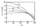
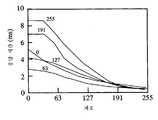
이상과 같이 해서, 흑계조에서 중간조로의 스위칭에서는, 액정층이 두꺼운 오목부 부근의 고속의 스위칭이 지배적으로 되기 때문에, 액정의 응답시간이 단축된다. 도 7은, 요철형성에 의한 액정의 응답시간의 단축의 양상을 도시하는 도면이다. 횡축은 스위칭 후의 계조이고, 종축이 응답시간이다. 여기에서, 스위칭 전의 계조는 제로이다. 도7이 도시하는 바와 같이, 요철이 없는 종래의 액정 표시 장치에서는, 제로 계조에서 중간조로의 스위칭이 느리다. 한편, 요철을 설치한 액정 표시 장치에서는, 제로 계조에서 중간조로의 스위칭이 고속화되어 있다.As described above, in the switching from black to midtones, high-speed switching in the vicinity of the thick recess of the liquid crystal layer becomes dominant, so that the response time of the liquid crystal is shortened. 7 is a diagram showing an aspect of shortening the response time of liquid crystal due to the formation of unevenness. The horizontal axis represents the gray level after switching, and the vertical axis represents the response time. Here, the gradation before switching is zero. As shown in Fig. 7, in the conventional liquid crystal display device having no irregularities, the switching from zero gray scale to half gray scale is slow. On the other hand, in the liquid crystal display device provided with the unevenness, the switching from the zero grayscale to the halftone is speeded up.
또한, 본 발명에 의해 구동 전압의 증감에 따른 색조변화를 억제할 수 있다. 그것은, 다음에 기술하는 원리에 따른다.In addition, according to the present invention, color change due to the increase or decrease of the driving voltage can be suppressed. It follows the principle described next.
IPS 표시 모드에 있어서의 투과율(T)은, 일반적으로 다음 수학식 2로 나타내어진다.The transmittance T in the IPS display mode is generally represented by the following equation.

〔단, To:보정계수, χ:액정의 실효적인 광축과 입사광의 편광방향이 이루는 각, △neff:액정의 실효적인 굴절률 이방성, λ:입사광의 파장〕.(Where, To : correction coefficient, χ: angle between the effective optical axis of the liquid crystal and the polarization direction of incident light,Δn eff : effective refractive index anisotropy of the liquid crystal, λ: wavelength of incident light).
따라서, 액정의 실효적인 배향 방향과 입사광의 편광방향이 이루는 각(χ)이 π/4라디안(45도)일 때, 실효적인 리타데이션(d·△neff)의 2배의 파장(λ)의 광이 최대의 투과율을 나타낸다. 즉, 실효적인 리타데이션(d·△neff)이 변화되면, 투과율이 최대가 되는 파장이 변화되기 때문에, 색조가 변화된다.Therefore, when the angle χ formed between the effective alignment direction of the liquid crystal and the polarization direction of the incident light is π / 4 radians (45 degrees), the wavelength λ of twice the effective retardation d ·Δn eff The light has the maximum transmittance. In other words, when the effective retardation d ·Δn eff is changed, the wavelength at which the transmittance is maximized is changed, whereby the color tone is changed.
여기에서 본 발명에 따르면, 전계가 인가되었을 때, 액정층의 두께(d)가 두꺼운 영역, 즉, 실효적인 리타데이션(d·△neff)이 큰 영역에서 스위칭이 시작된다. 즉, 구동전압이 낮은 때라도 이미 d·△neff가 커지고, 투과율이 최대가 되는 파장이 길고, 황색이 강조된다. 그 때문에, 도 2 내지 도 4에 도시한 액정층에 두께의 변화가 없는 종래의 액정 표시 장치에 있어서의, 구동전압의 증대에 따라 색조가 청색에서 황색으로 변화된다고 하는 문제를 보정할 수 있다.According to the present invention, when an electric field is applied, switching starts in a region where the thickness d of the liquid crystal layer is thick, that is, in a region where the effective retardation d ·Δn eff is large. That is, even when the driving voltage is low, d ·Δn eff is already increased, the wavelength at which the transmittance is maximum is long, and yellow is emphasized. Therefore, in the conventional liquid crystal display device in which there is no change in thickness in the liquid crystal layers shown in Figs. 2 to 4, the problem that the color tone changes from blue to yellow can be corrected as the driving voltage increases.
본 발명은 부분적으로 탄성 에너지가 낮은 영역이 있으면, 그 영역에서 스위칭이 시작된다고 하는 원리에 근거하고 있다. 그 때문에, 본 발명을 적용하기 위해서는, 광 투과 영역에서 액정층의 두께의 변동이 있으면 좋고, 요철의 형상은 일절 한정되지 않는다. 요철은 뾰족해져 있어도 좋고, 둥글게 되어 있어도 좋다. 또, 오목부와 볼록부의 면적비도 한정되지 않는다. 단, 요철의 형상이나 오목부와 볼록부의 면적비가 변경되면, 고속화의 효과의 크기나 고속화되는 계조, 및 구동전압의 증감에 따른 색조 변화를 억제하는 효과의 크기가 변화된다. 단, 효과를 크게 하기 위해서는, 액정층의 두께가 어느 정도 이상인 것이 바람직하다.The invention is based, in part, on the principle that if there is an area with low elastic energy, switching starts in that area. Therefore, in order to apply this invention, what is necessary is just the fluctuation | variation of the thickness of a liquid crystal layer in a light transmission area | region, and the shape of an unevenness | corrugation is not limited at all. The unevenness may be pointed or may be rounded. Moreover, the area ratio of a recessed part and a convex part is not limited, either. However, when the shape of the unevenness and the area ratio of the concave portion and the convex portion are changed, the magnitude of the effect of speeding up, the gradation of speeding up, and the magnitude of the effect of suppressing the change in color tone due to the increase or decrease of the driving voltage change. However, in order to enlarge an effect, it is preferable that the thickness of a liquid crystal layer is more than a grade.
다음에, 본 발명의 실시 형태를 도면에 근거하여, 보다 구체적으로 설명한다.EMBODIMENT OF THE INVENTION Next, embodiment of this invention is described more concretely based on drawing.
〔실시 형태 1〕[Embodiment 1]
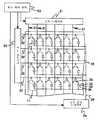
본 발명의 실시 형태 1의 구성을 도 1, 도 2 및 도 5를 이용해서 설명한다.The structure of
본 실시 형태 1의 액정 표시 장치는, 도 2에 도시하는 바와 같이, 화소 전극(35)에 신호전위를 공급하는 신호 드라이버(51)와, 화소를 선택하는 전위를 공급하는 주사 드라이버(52)와, 공통 전극(36)에 전위를 공급하는 공통 전극 드라이버(54)와, 신호 드라이버(51) 및 주사 드라이버(52) 및 공통 전극 드라이버(54)를 제어하는 표시 제어 장치(53)를 포함한다.As shown in FIG. 2, the liquid crystal display of the first embodiment includes a
기판(1)에는, 주사 드라이버(52)에 접속된 복수의 주사선(32)과, 신호 드라이버(51)에 접속되고, 또한 주사선(32)과 교차한 신호선(31)과, 주사선(32)과 신호선(31)의 교점부근에 대응해서 배치되어, 주사선(32)과 신호선(31)과 전기적으로 접속된 제1 TFT(33)와, 제1 TFT(33)에 전기적으로 접속되어, 신호선(31)에 대응한 화소 전극(35)과, 화소 전극(35)에 대응한 공통 전극(36)과, 공통 전극(36)과 공통 전극 드라이버(54)에 전기적으로 접속된 공통 전극 접속부(36')가 구비되어 있다.The
신호선(31)과 주사선(32)에 둘러싸인 하나의 영역에 대응해서 하나의 화소(11)가 형성되고, 복수의 화소(11)에 의해 표시부(22)가 형성되어 있다.One
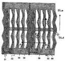
도 1은 실시 형태 1의 화소 근방의 회로배치 패턴 구성을 도시하는 도면이 다. 주사선(32)과 신호선(31)은 서로 교차하고, 주사선(32)과 신호선(31)에 둘러싸인 영역에 대응해서 화소(11)가 형성되어 있다. 제1 TFT(33)는 주사선(32)과 신호선(31)의 교점부근에 대응해서 배치되어, 주사선(32)과 신호선(31)과 화소 전극(35)에 전기적으로 접속되어 있다. 공통 전극(36)은 화소 전극(35)에 대응해서 배치되어, 공통 전극(36)과 화소 전극(35)으로 기판면에 대해서 평행한 성분을 가지는 전계를 발생시킨다. 화소 전극(35)과 공통 전극(36)과 신호선(31)은 하나의 화소 내에서 1회 이상 절곡되어, 멀티 도메인을 형성하고 있다. 제2 절연막(86)은, 화소 전극(35)과 공통 전극(36) 사이의 광 투과 영역에 배치되어, 액정층(34)의 두께를 변동시키고 있다.FIG. 1 is a diagram showing a circuit arrangement pattern configuration near the pixel of
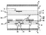
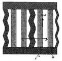
도 5는 도 1의 A-A'단면의 단면도이다. 재질이 투명 유리인 기판(1)과, 기판(1)에 대향 배치되고, 재질이 투명 유리인 기판(2)과, 기판(1)과 기판(2)으로 협지된 액정층(34)을 가진다.5 is a cross-sectional view taken along the line AA ′ of FIG. 1. It has the board |
기판(1)은 공통 전극(36)과, 주사선(32)(도 5에 도시되지 않는다)과, 제1 절연막(81)을 통해 공통 전극(36)보다도 상층에 배치된 신호선(31)과, 공통 전극(36)에 대응하고, 기판(1)면에 대해서 평행한 성분을 가지는 전계를 발생시키는 화소 전극(35)과, 화소 전극(35) 위에 구비된 보호막(82)과, 보호막(82) 위에 구비되어, 액정층(34)의 두께를 변동시키는 요철을 형성하고 있는 제2 절연막(86)과, 제2 절연막(86) 위에 구비된 배향막(85)과, 기판(1)의 액정에 면하지 않는 쪽의 면 위에 구비되어, 액정의 배향 상태에 따라서 광학 특성을 바꾸는 수단인 편광판(6)을 가진다.The
공통 전극(36), 화소 전극(35), 신호선(31)은 막 두께가 0.2㎛정도의 도전체이고, CrMo나 Al이나 ITO(Indium Tin Oxide) 등을 이용할 수 있다. 제1 절연막(81), 보호막(82)은 막 두께가 각각 0.3㎛, 0.8㎛정도의 절연체이고, 질화규소 등을 이용할 수 있다. 제2 절연막(86)은 막 두께가 1㎛정도의 절연체이고, 요철에 의한 단차를 두기 위해서 형성된 것이다. 무기물질도 유기물질도 이용할 수 있다. 또한, 본 발명이 상기의 막 두께나 재질로 한정되는 것이 아닌 것은, 말할 필요도 없다.The
기판(2)은 불필요한 간극부로부터의 광을 차광하는 차광막(5)과, 차광막(5) 위에 구비되어, R, G, B에 대응한 색을 표현하는 컬러 필터(4)와, 카라 필터(4) 위에 구비되어, 요철을 평탄화하는 평탄화 막(3)과, 평탄화 막(3) 위에 구비된 배향막(85)과, 기판(2)의 액정에 면하지 않는 쪽의 면 위에 구비된 편광판(6)을 가진다.The board |
배향막(85)에는 액정을 배향시키기 위한 러빙 처리가 되어 있다. 러빙 방향은 신호선의 연신 방향(DLa)에 평행하다. 굴곡된 화소 전극의 1변과 러빙 방향이 이루는 각은 15도이고, IPS 표시 모드에 대응하고 있다.The
편광판(6)의 투과축은 각각의 편광판(6)이 배치되어 있는 기판상의 배향막(85)의 러빙 방향에 대해서 평행 또는 수직으로 향해져 있고, 기판(1)의 편광판과 기판(2)의 편광판은 크로스 니콜로 배치되어, 노멀리 블랙 모드에 대응하고 있다. 또한, 본 발명이 상기의 러빙 각도로 한정되는 것이 아닌 것, 또한, 노멀리 화이트 모드에도 적용할 수 있는 것은, 말할 필요도 없다.The transmission axis of the
기판(1)과 기판(2)의 사이에는 비즈가 분산되어, 액정층(34)의 두께를 확보하고 있다. 비즈는 볼록부에도 존재하기 때문에, 볼록부상의 비즈에 의해 액정층의 두께가 결정된다. 그 때문에, 각 화소의 액정층의 두께의 평균치를 패널 전체에 걸쳐서 균일하게 하기 위해서는, 볼록부의 면적이 넓은 쪽이 바람직하다. 그 때문에, 신호선(31)상이나 주사선(32)상과 같이, 화소 내의 표시 영역 외에도, 요철을 형성하기 위한 제2 절연막(86)이 배치되어 있다. 또한, 제2 절연막 대신에 주상 스페이서를 적용할 수 있는 것은 말할 필요도 없다.Beads are dispersed between the board |
비즈의 지름은 3㎛정도, 따라서 액정층(34)의 두께는 4㎛정도, 액정층(34)의 굴절률 이방성은 0.1정도이고, 이 조합에 의해 리타데이션이 조정된다. 또한, 본 발명이 상기의 리타데이션으로 한정되는 것이 아닌 것은, 말할 필요도 없다.The diameter of the beads is about 3 μm, so that the thickness of the
백 라이트(도시하지 않음)에 대한 제약은 없고 직하형 방식의 것도 사이드 라이트 방식의 것도 사용할 수 있다.There is no restriction on the backlight (not shown), and a direct type or side light type can be used.
구동은 액티브 매트릭스 구동에 의해 행해진다.The drive is performed by active matrix drive.
본 발명에 따르면, 액정층의 두께가 변동되어 있기 때문에, 액정층이 두꺼운 오목부에서는 탄성 에너지가 낮고, 화소 전극(35)과 공통 전극(36)의 사이에 전계가 인가되었을 때에, 오목부의 영역에서 스위칭이 시작된다. 그 때문에, 제로 계조에서 중간조로의 스위칭을 고속화할 수 있고, 동화 표시 품질이 뛰어난 액정 표시 장치를 제공할 수 있다.According to the present invention, since the thickness of the liquid crystal layer is varied, the elastic energy is low in the concave portion where the liquid crystal layer is thick, and when the electric field is applied between the
또한, 요철의 형성에 제2 절연막(86)을 이용하지 않고, 보호막(82)으로 요철을 형성해도 본 발명을 적용할 수 있는 것은 말할 필요도 없다.It goes without saying that the present invention can be applied even when the unevenness is formed by the
더욱이, 제2 절연막(86)의 유무에 따라 요철을 형성하는 것이 아니고, 요철이 있는 제2 절연막을 표시부(22) 전면에 형성함으로써, 액정층(34)의 두께를 광 투과 영역에서 변동시켰을 경우에도 본 발명을 적용할 수 있는 것은 말할 필요도 없다.In addition, when the thickness of the
〔비교예 1〕[Comparative Example 1]
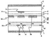
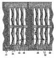
본 발명의 비교예 1은, 실시 형태 1에 비교할 때 제2 절연막(86)이 형성되지 않고, 액정층(34)의 두께가 광 투과 영역에서 거의 일정한 것만이 다르다.In Comparative Example 1 of the present invention, the second insulating
도 3은 비교예 1의 화소 근방의 회로배치 패턴 구성을 도시하는 도면이다. 실시 형태 1과 달리 제2 절연막이 형성되어 있지 않다.3 is a diagram showing a circuit arrangement pattern configuration near the pixel of Comparative Example 1. FIG. Unlike the first embodiment, no second insulating film is formed.
도 4는 도 3의 A-A'단면의 단면도이다. 실시 형태 1과 달리 제2 절연막이 없고 액정층의 두께가 거의 일정하다.4 is a cross-sectional view taken along the line AA ′ of FIG. 3. Unlike the first embodiment, there is no second insulating film and the thickness of the liquid crystal layer is almost constant.
그 때문에, 제로 계조에서 중간조에의 액정의 응답시간이, 실시 형태 1에 비해 느리다.Therefore, the response time of the liquid crystal from the zero grayscale to the halftone is slower than in the first embodiment.
〔실시 형태 2〕[Embodiment 2]
실시 형태 2는 실시 형태 1에 비교했을 때 제2 절연막(86)의 형상이 다를 뿐이다. 따라서, 이것에 대해서 도 8 및 도 9를 이용해서 설명한다.In the second embodiment, the shape of the second insulating
도 8은 실시 형태 2의 화소 근방의 회로배치 패턴 구성을 도시하는 도면이다. 실시 형태 1과 달리, 제2 절연막의 형상과 배치가 무작위로 형성되어 있다.FIG. 8 is a diagram showing a circuit arrangement pattern configuration near the pixel of
도 9는 도 8의 A-A'단면의 단면도이다. 실시 형태 1과 달리 제2 절연막의 형상과 배치와 요철의 높이가 무작위로 형성되어 있다.9 is a cross-sectional view taken along the line AA ′ of FIG. 8. Unlike
단, 하나의 화소 내의 오목부와 볼록부의 면적비나, 요철의 높이의 평균치는, 각 화소 사이에서 일치하고 있는 것이 바람직하다. 불일치할 경우에는, 각 화소마다 고속화의 효과의 크기가 변화하게 되고, 휘도 얼룩 등의 문제를 일으키는 원인이 된다.However, it is preferable that the average ratio of the area ratio of the concave portion and the convex portion and the height of the unevenness in one pixel coincide between the pixels. If there is a mismatch, the magnitude of the speed-up effect changes for each pixel, causing problems such as luminance unevenness.
본 발명에 따르면, 실시 형태 1과 같이, 액정층의 두께가 변동되어 있기 때문에, 액정층이 두꺼운 오목부에서는 탄성 에너지가 낮고, 화소 전극(35)과 공통 전극(36)의 사이에 전계가 인가되었을 때에, 오목부의 영역에서 스위칭이 시작된다. 그 때문에, 제로 계조에서 중간조로의 스위칭을 고속화할 수 있고, 동화 표시 품질이 뛰어난 액정 표시 장치를 제공할 수 있다.According to the present invention, since the thickness of the liquid crystal layer is varied as in the first embodiment, the elastic energy is low in the concave portion where the liquid crystal layer is thick, and an electric field is applied between the
〔실시 형태 3〕[Embodiment 3]
실시 형태 3은 실시 형태 1에 비교할 때, 제2 절연막의 형상과 배치가 다르다. 이것에 대해서 도 10 및 도 11을 이용해서 설명한다.In the third embodiment, the shape and arrangement of the second insulating film are different from those in the first embodiment. This will be described with reference to FIGS. 10 and 11.
도 10은 실시 형태 3의 화소 근방의 회로배치 패턴 구성을 도시하는 도면이다. 또, 도 11은 도 10의 A-A'단면의 단면도이다.10 is a diagram showing a circuit arrangement pattern configuration near the pixel of the third embodiment. 11 is a cross-sectional view taken along the line AA ′ of FIG. 10.
본 실시 형태는 실시 형태 1과 달리, 제2 절연막(86)에 의해 형성되는 요철에 따른 단차가 화소 전극(35)과 공통 전극(36)의 사이에 하나만 있다. 또, 화소 전극(35)이 볼록부에 중첩되어 배치되고, 공통 전극(36)은 오목부에 중첩되어 있다.In the present embodiment, unlike the first embodiment, there is only one step between the
이것에 의해, 요철의 패턴 폭이 실시 형태 1에 비해 커지고, 제2 절연막(86)의 가공이 용이해진다.As a result, the pattern width of the unevenness becomes larger than that of the first embodiment, and the processing of the second insulating
〔실시 형태 4〕[Embodiment 4]
실시 형태 4는 실시 형태 3에 비교할 때 전극과 제2 절연막의 배치가 다르다. 이것에 대해서 도 12 및 도 13을 이용해서 설명한다.In the fourth embodiment, the arrangement of the electrodes and the second insulating film is different from that in the third embodiment. This will be described with reference to FIGS. 12 and 13.
도 12는 실시 형태 4의 화소 근방의 회로배치 패턴 구성을 도시하는 도면이다. 또, 도 13은 도 12의 A-A'단면의 단면도이다.12 is a diagram showing a circuit arrangement pattern configuration near the pixel of the fourth embodiment. FIG. 13 is a cross-sectional view taken along the line AA ′ of FIG. 12.
실시 형태 4는 실시 형태 3과 달리, 화소 전극(35) 및 신호선(31)이 제2 절연막(86)보다 상층에 배치되어 있다. 또한, 공통 전극(36)은 주사선(32)(도 13에 도시되지 않는다)과 함께 기판(1) 위에 배치되어 있다. 여기에서, 실시 형태 3에서는, 도 11에서 알 수 있는 바와 같이, 화소 전극(35)과 공통 전극(36)의 사이에 발생하는 전계의 전기 역선(21) 중, 액정층을 통과하는 전기 역선(21)의 대부분은 제2 절연막(86)도 통과한다. 바꿔 말하면, 액정층(34)은 제2 절연막(86)을 통해서 전계가 인가된다. 한편, 실시 형태 4에서는, 도 13에서 알 수 있는 바와 같이, 화소 전극(35)이 제2 절연막(86)보다 상층에 배치되어 있기 때문에, 제2 절연막(86)을 통하지 않고서 액정층(34)에 전계가 인가된다. 그 때문에, 실시 형태 4에서는 실시 형태 3보다 구동전압을 저하시킬 수 있다.In the fourth embodiment, unlike the third embodiment, the
또한, 보호막(82)이 형성되어 있지 않은 경우, 보호막(82)과 제2 절연막(86)이 일괄 가공되어 있는 경우, 보호막(82)과 제2 절연막(86)이 동일 재료로 일체화 되어 있는 경우에 있어서도, 액정층(34)의 두께를 변동시킬 수 있기 때문에, 본 발명을 적용할 수 있는 것은 말할 필요도 없다.In addition, when the
〔실시 형태 5〕[Embodiment 5]
실시 형태 5는 실시 형태 4에 비교할 때 제2 절연막의 배치가 다르다. 이것에 대해서 도 14, 도 15 및 도 16을 이용해서 설명한다.In the fifth embodiment, the arrangement of the second insulating film is different from that in the fourth embodiment. This will be described with reference to FIGS. 14, 15, and 16.
도 14는 실시 형태 5의 기판(1) 위의 화소 근방의 회로배치 패턴 구성을 도시하는 도면이다. 또, 도 15는 실시 형태 5의 기판(2) 위의 화소 근방의 회로배치 패턴 구성을 도시하는 도면이다. 도 16은, 도 14의 A-A'단면의 단면도이다.FIG. 14 is a diagram showing a circuit arrangement pattern configuration near the pixel on the
기판(1)은 공통 전극(36)과, 주사선(32)(도 16에 도시되지 않는다)과, 제1 절연막(81)을 통해 공통 전극(36)보다도 상층에 배치된 신호선(31)과, 화소 전극(35)을 구비하고, 기판(1)면에 대해서 평행한 성분을 가지는 전계를 발생시키는 화소 전극(35)과, 화소 전극(35) 위에 구비된 보호막(82)과, 보호막(82) 위에 구비된 배향막(85)과, 기판(1)의 액정에 면하지 않는 쪽의 면 위에 구비되고, 액정의 배향 상태에 따라 광학 특성을 바꾸는 수단인 편광판(6)을 가진다.The
기판(2)은 불필요한 간극부로부터의 광을 차광하는 차광막(5)과, 차광막(5) 위에 구비되어, R, G, B에 대응한 색을 표현하는 컬러 필터(4)와, 컬러 필터(4) 위에 구비되어, 요철을 평탄화하는 평탄화 막(3)과, 평탄화 막(3) 위에 구비되어, 액정층(34)의 두께를 변동시키는 요철을 형성하고 있는 제2 절연막(86)과, 제2 절연막(86) 위에 구비된 배향막(85)과, 기판(2)의 액정에 면하지 않는 쪽의 면 위에 구비된 편광판(6)을 가진다.The
실시 형태 5는 실시 형태 4와 달리, 액정층의 두께를 변동시키는 요철을 형성하는 제2 절연막(86)이 기판(2) 위에 배치되어 있다. 그 때문에, 화소 전극(35)이나 공통 전극(36)이나 신호선(31)이나 주사선(32) 등의 배선 또는 전극과 제2 절연막(86)이 떨어져 있기 때문에, 제2 절연막(86)의 막 두께가 변동하는 경우에도, 화소 전극(35)과 공통 전극(36)의 사이 등의 부유용량이 변동되지 않고, 표시 얼룩 등을 유발시키기 어려워진다.In the fifth embodiment, unlike the fourth embodiment, a second insulating
〔실시 형태 6〕[Embodiment 6]
실시 형태 6은 실시 형태 5에 비교할 때 제2 절연막의 배치와 형상이 다르다. 이것에 대해서 도 14, 도 17, 도 18 및 도 19를 이용해서 설명한다.The sixth embodiment differs in arrangement and shape of the second insulating film as compared with the fifth embodiment. This is demonstrated using FIG. 14, FIG. 17, FIG. 18, and FIG.
실시 형태 6의 기판(1) 위의 화소 근방의 회로배치 패턴 구성을 도시하는 도면은 도 14와 동일하다. 또, 도 17은 실시 형태 6의 기판(2) 위의 화소 근방의 회로배치 패턴 구성을 도시하는 도면이다. 도 18은, 도 17의 A-A'단면의 단면도이다. 도 19는 도 14 및 도 17의 B-B'단면의 단면도이다.14 is a view showing the circuit arrangement pattern configuration near the pixel on the
실시 형태 6에서는, 제2 절연막(86)에 의해 형성되는 요철의 연신 방향(DLb)이, 화소 전극의 연신 방향(DLc)에서 어긋나 있고, 거의 수직으로 교차하고 있다. 그 때문에, 기판(1)과 기판(2)의 사이에 오정렬이 생긴 경우에도, 차광막(5)에 대한 제2 절연막(86)의 지위관계는 화소마다 변화하지 않고, 화소 전극(35)과 공통 전극(36) 사이의 영역 하나하나에서, 오목부와 볼록부의 면적비가 변동하지 않고, 액정의 응답시간의 단축의 효과가 변동되지 않는다.In
〔실시 형태 7〕[Embodiment 7]
실시 형태 7은 실시 형태 6에 비교할 때 제2 절연막의 배치와 형상이 다르다. 이것에 대해서 도 14, 도 20 및 도 21을 이용해서 설명한다.The seventh embodiment differs in arrangement and shape of the second insulating film as compared with the sixth embodiment. This will be described with reference to FIGS. 14, 20, and 21.
실시 형태 7의 기판(1) 위의 화소 근방의 회로배치 패턴 구성은 도 14와 같다. 또, 도 20은 실시 형태 7의 기판(2) 위의 화소 근방의 회로배치 패턴 구성을 도시하는 도면이다. 도 21은, 도 20의 A-A'단면의 단면도이다.The circuit arrangement pattern structure in the vicinity of the pixel on the
실시 형태 7에서는, 제2 절연막(86)에 의해 형성되는 요철에 따른 단차의 연신 방향(DLd)이 액정의 초기 배향 방향(DLe)과 일치하고 있다. 그 때문에, 배향막(85)에 러빙 처리를 실시할 때에, 광 투과 영역에 있어서 요철에 따른 단차를 타 넘지 않아, 균일하게 러빙 처리를 실시할 수 있고, 배향 불량 등을 유발시키기 어렵다.In Embodiment 7, the extending | stretching direction DLd of the level | step difference resulting from the unevenness | corrugation formed by the 2nd insulating
〔실시 형태 8〕[Embodiment 8]
실시 형태 8은 실시 형태 7에 비교할 때 제2 절연막의 배치와 형상이 다르다. 이것에 대해서 도 22 및 도 23을 이용해서 설명한다.The eighth embodiment differs in arrangement and shape of the second insulating film as compared with the seventh embodiment. This will be described with reference to FIGS. 22 and 23.
도 22는 실시 형태 8의 기판(1) 위의 화소 근방의 회로배치 패턴 구성을 도시하는 도면이다. 또, 도 23은 도 22의 A-A'단면의 단면도이다.22 is a diagram showing a circuit arrangement pattern configuration near the pixel on the
기판(1)은 공통 전극(36)과, 주사선(32)(도 23에 도시되지 않는다)과, 공통 전극(36) 위에 배치된 제1 절연막(81)과, 제1 절연막(81) 위에 배치된 보호막(82)과, 보호막(82) 위에 배치되어, 액정층(34)의 두께를 변동시키는 요철을 형성하고 있는 제2 절연막(86)과, 제2 절연막(86) 위에 배치된 신호선(31)과, 제2 절연막(86)보다 상층에 배치되어, 공통 전극(36)에 대응해서 기판(1)면에 대해서 평행한 성분을 가지는 전계를 발생시키는 화소 전극(35)과, 화소 전극(35) 위에 배치된 배향막(85)과, 기판(1)의 액정에 면하지 않는 쪽의 면 위에 구비되어, 액정의 배향 상태에 따라서 광학 특성을 바꾸는 수단인 편광판(6)을 가진다. 또한, 공통 전극(36)은 주사선(32)과 함께 기판(1) 위에 배치되어 있다.The
기판(2)은 불필요한 간극부로부터의 광을 차광하는 차광막(5)과, 차광막(5) 위에 구비되어, R, G, B에 대응한 색을 표현하는 컬러 필터(4)와, 컬러 필터(4) 위에 구비되어, 요철을 평탄화하는 평탄화 막(3)과, 평탄화 막(3) 위에 구비된 배향막(85)과, 기판(2)의 액정에 면하지 않는 쪽의 면 위에 구비된 편광판(6)을 가진다.The
실시 형태 8은 실시 형태 7과 달리, 액정층의 두께를 변동시키는 요철을 형성하는 제2 절연막(86)이 기판(1) 위에 배치되어 있다. 그 때문에, 기판(1)과 기판(2)의 사이에 오정렬이 생긴 경우에도, 제2 절연막(86)은 영향을 받지 않기 때문에, 전 화소에 걸쳐 액정의 응답시간의 단축의 효과가 변동되지 않는다.In the eighth embodiment, unlike the seventh embodiment, a second insulating
또, 실시 형태 8은 실시 형태 4와 달리, 제2 절연막(86)에 의해 형성되는 요철에 따른 단차의 연신 방향(DLd)이, 액정의 초기 배향 방향(DLe)과 일치하고 있다. 그 때문에, 배향막(85)에 러빙 처리를 실시할 때에, 광 투과 영역에 있어서 요철에 따른 단차를 타 넘지 않아, 균일하게 러빙 처리를 실시할 수 있고, 배향 불량 등을 유발시키지 않는다.Moreover, in
〔실시 형태 9〕[Embodiment 9]
실시 형태 9는 실시 형태 8에 비교할 때 제2 절연막(86)과 화소 전극(35)과 공통 전극(36)의 배치와 형상이 다를 뿐이다. 따라서, 이것에 대해서 도 24를 이용해서 설명한다.In the ninth embodiment, the arrangement and the shape of the second insulating
도 24는 실시 형태 9의 기판(1) 위의 화소 근방의 회로배치 패턴 구성을 도시하는 도면이다. 실시 형태 9는, 실시 형태 8과 달리, 화소 전극(35) 및 공통 전극(36)이 굴곡되어 있지 않다. 그 때문에, 러빙 방향은 신호선(31)의 연신 방향에 대해서 15도 기울어 있다. 단, 화소 전극(35)의 1변과 러빙 방향이 이루는 각이 15도인 것은 실시 형태 8과 같다.24 is a diagram showing a circuit arrangement pattern configuration near the pixel on the
제2 절연막(86)에 의해 형성되는 요철에 따른 단차의 연신 방향은 신호선(31)의 연신 방향에 대해서 15도 기울어 있다. 단, 제2 절연막(86)에 의해 형성되는 요철에 따른 단차의 연신 방향(DLd)이, 액정의 초기 배향 방향(DLe)과 일치하고 있는 것은 실시 형태 8과 같다.The extending direction of the step due to the unevenness formed by the second insulating
그 때문에, 실시 형태 8과 같이, 실시 형태 9에서는, 배향막(85)에 러빙 처리를 실시할 때에, 광 투과 영역에 있어서 요철에 따른 단차를 타 넘지 않아, 균일하게 러빙 처리를 실시할 수 있고, 배향 불량 등을 유발시키지 않는다.Therefore, in the ninth embodiment as in the eighth embodiment, when the rubbing treatment is performed on the
〔실시 형태 10〕[Embodiment 10]
실시 형태 10은 실시 형태 8에 비교할 때 제2 절연막의 배치와 형상이 다르다. 이것에 대해서 도 25 및 도 26을 이용해서 설명한다.The tenth embodiment is different from the arrangement and shape of the second insulating film when compared with the eighth embodiment. This will be described with reference to FIGS. 25 and 26.
도 25는 실시 형태 10의 기판(1) 위의 화소 근방의 회로배치 패턴 구성을 도시하는 도면이다. 또, 도 26은 도 25의 A-A'단면의 단면도이다.FIG. 25 is a diagram showing a circuit arrangement pattern configuration near the pixel on the
실시 형태 10은 실시 형태 8과 달리, 화소 전극(35) 및 공통 전극(36)이 제2 절연막(86)에 의한 요철에 따른 단차를 타 넘지 않고 있다. 예를 들면, 실시 형태 8의 도 22에 도시하는 부분C에서는, 화소 전극(35)이 제2 절연막(86)의 끝을 타 넘고 있다. 한편, 실시 형태 10의 도 25에 도시하는 부분C에서는, 화소 전극(35)은 제2 절연막(86)을 타 넘지 않고 있다. 즉, 도 22에서는 A-A'단면에 평행한 단면을 취한 경우에, 화소 전극(35)이 제2 절연막(86) 위(단차의 상부)에 있는 개소와 보호막(82) 위(단차의 하부)에 있는 개소가 존재하는 것에 대해서, 도 25에서는, 제2 절연막(86)은 화소 전극(35)을 피해서 배치되어 있고, A-A'단면에 평행한 어느 단면을 취하더라도, 화소 전극(35)이 보호막(82) 위(단차의 하부)에 있다.In the tenth embodiment, unlike the eighth embodiment, the
그 때문에, 실시 형태 10에서는, 제2 절연막(86)에 의한 요철에 따른 단차에 의해 화소 전극(35)이 끊어진다고 하는 것 등의 불량이 생기지 않는다.Therefore, in the tenth embodiment, no defect such as the disconnection of the
〔실시 형태 11〕[Embodiment 11]
실시 형태 11은 실시 형태 10에 비교할 때 제2 절연막의 배치와 형상이 다르다. 이것에 대해서 도 27 및 도 28을 이용해서 설명한다.The eleventh embodiment is different from the arrangement and shape of the second insulating film when compared with the tenth embodiment. This will be described with reference to FIGS. 27 and 28.
도 27은 실시 형태 11의 기판(1) 위의 화소 근방의 회로배치 패턴 구성을 도 시하는 도면이다. 또, 도 28은 도 27의 A-A'단면의 단면도이다.27 is a diagram showing the circuit arrangement pattern configuration near the pixel on the
실시 형태 11은 실시 형태 10과 달리, 제2 절연막(86)에 의한 요철에 따른 단차가, 화소 전극(35) 및 공통 전극(36)과 중첩되어 있다. 예를 들면, 실시 형태 10의 도 25에 도시하는 부분C에서는, 제2 절연막(86)에 의한 요철에 따른 단차가 화소 전극(35)에 중첩되어 있지 않다. 한편, 실시 형태 11의 도 27에 도시하는 부분C에서는, 제2 절연막(86)에 의한 요철에 따른 단차가 화소 전극(35)에 중첩되어 있다.In the eleventh embodiment, unlike the tenth embodiment, the step due to the unevenness caused by the second insulating
그 때문에, 실시 형태 11에서는, 제2 절연막(86)에 의한 요철에 따른 단차부분에서 러빙 처리가 불충분해지고, 배향 불량이 생긴 경우라도, 화소 전극(35) 및 공통 전극(36)이 불투명한 도전체이면, 그 불량은 화소 전극(35) 및 공통 전극(36)에 의해 숨겨지기 때문에, 표시에는 영향을 주지 않는다.Therefore, in the eleventh embodiment, even when the rubbing process becomes insufficient at the stepped portion due to the unevenness caused by the second insulating
또, 실시 형태 11은, 실시 형태 10과 같이, 제2 절연막(86)에 의한 요철에 따른 단차가, 화소 전극(35) 및 공통 전극(36)과 중첩되어 있지만, 타 넘지 않고 있다. 즉, 도 27에서는, 제2 절연막(86)은 대체로 화소 전극(35)을 피해서 배치되어 있지만, 화소 전극(35)은 단부에서 제2 절연막(86) 위에 얹혀 있다. 이것 때문에, A-A'단면에 평행한 어느 단면을 취하더라도, 화소 전극(35)은 대체로 보호막(82) 위(단차의 하부)에 있고, 단부만 제2 절연막(86) 위(단차의 상부)에 있다.In addition, in the eleventh embodiment, the step due to the unevenness due to the second insulating
그 때문에, 실시 형태 10과 같이, 제2 절연막(86)에 의한 요철에 따른 단차에 의해 화소 전극(35)이 끊어진다고 하는 것 등의 불량이 생기지 않는다.Therefore, as in the tenth embodiment, a defect such as that the
〔실시 형태 12〕[Embodiment 12]
실시 형태 12는, 실시 형태 9에 비교할 때, 제2 절연막의 배치와 형상이 다르다. 이것에 대해서 도 29를 이용해서 설명한다.In the twelfth embodiment, compared with the ninth embodiment, the arrangement and the shape of the second insulating film are different. This will be described with reference to FIG. 29.
도 29는 실시 형태 12의 기판(1) 위의 화소 근방의 회로배치 패턴 구성을 도시하는 도면이다.29 is a diagram showing a circuit arrangement pattern configuration near the pixel on the
실시 형태 12는 실시 형태 9와 달리, 화소 전극(35) 및 공통 전극(36)이 제2 절연막(86)에 의한 요철에 따른 단차를 타 넘지 않고 있다. 예를 들면, 실시 형태 9의 도 24에 도시하는 부분C에서는, 화소 전극(35)이 제2 절연막(86)의 끝을 타 넘고 있다. 한편, 실시 형태 12의 도 29에 도시하는 부분C에서는, 화소 전극(35)은 제2 절연막(86)에 일부 중첩되어 있지만 타 넘지는 않고 있다. 즉, 도 29에서는, 제2 절연막(86)은 대체로 화소 전극(35)을 피해서 배치되어 있지만, 화소 전극(35)은 단부에서 제2 절연막(86) 위에 얹혀 있다. 이것 때문에, 횡축에 평행한 어느 단면을 취하더라도, 화소 전극(35)은 대체로 보호막(82) 위(단차의 하부)에 있고, 단부만 제2 절연막(86) 위(단차의 상부)에 있다.In the twelfth embodiment, unlike the ninth embodiment, the
그 때문에, 실시 형태 12에서는, 실시 형태 10과 같이, 제2 절연막(86)에 의한 요철에 따른 단차에 의해 화소 전극(35)이 끊어진다고 하는 것 등의 불량이 생기지 않는다.Therefore, in the twelfth embodiment, as in the tenth embodiment, a defect such as the disconnection of the
또한, 제2 절연막(86)에 의한 요철에 따른 단차가, 화소 전극(35) 및 공통 전극(36)과 중첩되어 있다.In addition, the step due to the unevenness caused by the second insulating
그 때문에, 실시 형태 12에서는, 제2 절연막(86)에 의한 요철에 따른 단차부분에서 러빙 처리가 불충분해지고, 배향 불량이 생긴 경우라도, 화소 전극(35) 및 공통 전극(36)이 불투명한 도전체이면, 그 불량은 화소 전극(35) 및 공통 전극(36)에 의해 숨겨지기 때문에, 표시에는 영향을 주지 않는다.Therefore, in the twelfth embodiment, even when the rubbing treatment becomes insufficient at the stepped portion due to the unevenness caused by the second insulating
〔실시 형태 13〕[Embodiment 13]
실시 형태 13은, 실시 형태 11에 비교할 때, 제2 절연막의 배치와 형상이 다르다. 이것에 대해서 도 30 및 도 31을 이용해서 설명한다.The thirteenth embodiment differs from the arrangement and shape of the second insulating film when compared with the eleventh embodiment. This will be described with reference to FIGS. 30 and 31.
도 30은 실시 형태 13의 화소 근방의 회로배치 패턴 구성을 도시하는 도면이다. 또, 도 31은 도 30의 A-A'단면의 단면도이다.30 is a diagram illustrating a circuit arrangement pattern configuration near the pixel of Embodiment 13; 31 is a sectional view taken along the line AA ′ of FIG. 30.
실시 형태 13은 실시 형태 11과 달리, 제2 절연막(86)에 의해 형성되는 요철에 따른 단차가, 화소 전극(35)과 공통 전극(36)의 사이에 하나만 있다. 또, 화소 전극(35)이 볼록부에 중첩되어 배치되고, 공통 전극은 오목부에 중첩되어 있다.In the thirteenth embodiment, unlike the eleventh embodiment, there is only one level difference due to the unevenness formed by the second insulating
이것에 의해, 요철의 패턴 폭이 실시 형태 11에 비해 커지고, 제2 절연막(86)의 가공이 용이해진다.As a result, the pattern width of the unevenness is larger than that of the eleventh embodiment, and the processing of the second insulating
또, 화소 전극(35)이 제2 절연막(86)보다 상층에 배치되어 있기 때문에, 제2 절연막(86)을 통하지 않고서 액정층(34)에 전계를 인가할 수 있고, 구동전압의 상승을 억제하고 있다.In addition, since the
또한, 제2 절연막(86)에 의해 형성되는 요철에 따른 단차의 연신 방향(DLd)이, 액정의 초기 배향 방향(DLe)과 일치하고 있기 때문에, 배향막(85)에 러빙 처리 를 실시할 때에, 광 투과 영역에 있어서 요철에 따른 단차를 타 넘지 않아, 균일하게 러빙 처리를 실시할 수 있고, 배향 불량 등을 유발시키기 어렵다.In addition, since the stretching direction DLd of the step due to the unevenness formed by the second insulating
또, 광 투과 영역에 있어서, 화소 전극(35) 및 공통 전극(36)이 제2 절연막(86)에 의한 요철에 따른 단차를 타 넘고 있지 않기 때문에, 단차에 의해 화소 전극(35)이 끊어지는 등의 불량이 생기지 않는다. 즉, 도 30에서는 화소 전극(35) 및 신호선(31)은 모두 제2 절연막(86) 위에 형성되고 있고, 단차에 걸리는 것은 아니다.In the light transmitting region, since the
〔실시 형태 14〕[Embodiment 14]
실시 형태 14는 실시 형태 13에 비교할 때 신호선(31)과 화소 전극(35)과 공통 전극(36)과 제2 절연막(86)의 형상과 배치가 다르다. 이것에 대해서 도 32 및 도 33을 이용해서 설명한다.In the fourteenth embodiment, the shape and arrangement of the
도 32는 실시 형태 14의 화소 근방의 회로배치 패턴 구성을 도시하는 도면이다. 주사선(32)과 신호선(31)은 서로 교차하고, 주사선(32)과 신호선(31)에 둘러싸인 영역에 대응해서 화소가 형성되어 있다. 제1 TFT(33)는 주사선(32)과 신호선(31)의 교점부근에 대응해서 배치되어, 주사선(32)과 신호선(31)과 화소 전극(35)에 전기적으로 접속되어 있다. 공통 전극(36)은 화소 전극(35)에 대응해서 배치되어, 공통 전극(36)과 화소 전극(35)으로 기판면에 대해서 평행한 성분을 가지는 전계를 발생시킨다. 화소 전극(35)과 공통 전극(36)과 신호선(31)은 하나의 화소 내에서 1회 이상 절곡되어, 멀티 도메인을 형성하고 있다. 제2 절연막(86)은, 화소 전극과 공통 전극 사이의 광 투과 영역에 배치되어, 액정층(34)의 두께를 변동시키고 있다. 신호선(31)과 공통 전극(36)은 제2 절연막(86)을 통해서 중첩되어 있다.32 is a diagram showing a circuit arrangement pattern configuration near the pixel of Embodiment 14; The
도 33은 도 32의 A-A'단면의 단면도이다. 재질이 투명 유리인 기판(1)과, 기판(1)에 대향 배치되고, 재질이 투명 유리인 기판(2)과, 기판(1)과 기판(2)으로 협지된 액정층(34)을 가진다.33 is a cross-sectional view taken along the line AA ′ of FIG. 32. It has the board |
기판(1)은 제1 절연막(81)과, 제1 절연막(81) 위에 배치된 신호선(31) 및 화소 전극(35)과, 신호선(31) 및 화소 전극(35) 위에 배치된 보호막(82)과, 보호막(82) 위에 배치된 제2 절연막(86)과, 제2 절연막(86)을 통해서 신호선(31)에 중첩되어 배치된 공통 전극(36)과, 액정(34)과의 계면에 배치된 배향막(85)과, 기판(1)의 액정에 면하지 않는 쪽의 면 위에 구비되어, 액정의 배향 상태에 따라서 광학 특성을 바꾸는 수단인 편광판(6)을 가진다. 또한, 공통 전극(36)은 주사선(32)(도 33에 도시되지 않는다)과 함께 제1 절연막(81) 위에 배치된다.The
공통 전극(36), 화소 전극(35), 신호선(31)은 막 두께가 0.2㎛정도의 도전체이고, CrMo나 Al이나 ITO(Indium Tin Oxide) 등을 이용할 수 있다. 제1 절연막(81), 보호막(82)은 막 두께가 각각 0.3㎛, 0.8㎛정도의 절연체이고, 질화규소 등을 이용할 수 있다. 제2 절연막(86)은 막 두께가 1㎛정도의 절연체이고, 무기물질도 유기물질도 이용할 수 있다. 또한, 본 발명이 상기의 막 두께로 한정되는 것이 아닌 것은, 말할 필요도 없다.The
기판(2)은 불필요한 간극부로부터의 광을 차광하는 차광막(5)과, 차광막(5) 위에 구비되어, R, G, B에 대응한 색을 표현하는 컬러 필터(4)와, 컬러 필터(4) 위에 구비되어, 요철을 평탄화하는 평탄화 막(3)과, 평탄화 막(3) 위에 구비된 배향막(85)과, 기판(2)의 액정에 면하지 않는 쪽의 면 위에 구비된 편광판(6)을 가진다.The
배향막(85)에는 액정을 배향시키기 위한 러빙 처리가 되어 있다. 러빙 방향은 신호선의 연신 방향에 평행하다. 굴곡된 화소 전극의 1변과 러빙 방향이 이루는 각은 15도이고, IPS 표시 모드에 대응하고 있다. 편광판(6)의 투과축은, 각각의 편광판이 배치되어 있는 기판상의 배향막의 러빙 방향에 대해서 평행 또는 수직으로 향해져 있고, 기판(1)의 편광판과 기판(2)의 편광판은 크로스 니콜로 배치되어, 노멀리 블랙 모드에 대응하고 있다. 또한, 본 발명이 상기의 러빙 각도로 한정되는 것이 아닌 것, 또한, 노멀리 화이트 모드에도 적용할 수 있는 것은, 말할 필요도 없다.The
기판(1)과 기판(2)의 사이에는 비즈가 분산되어, 액정층의 두께를 확보하고 있다. 비즈는 볼록부에도 존재하기 때문에, 볼록부상의 비즈에 의해 액정층의 두께가 결정된다. 그 때문에, 각 화소의 액정층의 두께의 평균치를 패널 전체에 걸쳐서 균일하게 하기 위해서는, 볼록부의 면적이 넓은 쪽이 바람직하다. 그 때문에, 신호선(31)상이나 주사선(32)상의 화소 내의 표시영역 외에도, 요철을 형성하기 위한 제2 절연막(86)이 배치되어 있다. 또한, 본 발명에 주상 스페이서를 적용할 수 있는 것은 말할 필요도 없다.Beads are dispersed between the board |
비즈의 지름은 3㎛정도, 액정층의 굴절률 이방성은 0.1정도이고, 이 조합에 의해 리타데이션이 조정된다. 또한, 본 발명이 상기의 리타데이션으로 한정되는 것이 아닌 것은 말할 필요도 없다.The diameter of the beads is about 3 µm and the refractive index anisotropy of the liquid crystal layer is about 0.1, and the retardation is adjusted by this combination. It goes without saying that the present invention is not limited to the above retardation.
백 라이트(도시하지 않음)에 대한 제약은 없고 직하형 방식의 것도 사이드 라이트 방식의 것도 사용할 수 있다.There is no restriction on the backlight (not shown), and a direct type or side light type can be used.
구동은 액티브 매트릭스 구동에 의해 행해진다.The drive is performed by active matrix drive.
실시 형태 14에 따르면, 액정층의 두께가 변동되어 있기 때문에, 액정층이 두꺼운 오목부에서는 탄성 에너지가 낮고, 화소 전극(35)과 공통 전극(36)의 사이에 전계가 인가되었을 때에, 오목부의 영역에서 스위칭이 시작된다. 그 때문에, 제로 계조에서 중간조로의 스위칭을 고속화할 수 있고, 동화 표시 품질이 뛰어난 액정 표시 장치를 제공할 수 있다.According to Embodiment 14, since the thickness of the liquid crystal layer is varied, the elastic energy is low in the concave portion having a thick liquid crystal layer, and when the electric field is applied between the
또, 전계가 인가되었을 때, 액정층의 두께(d)가 두꺼운 영역, 즉, 실효적인 리터데이션(d·△neff)이 큰 영역에서 스위칭이 시작되기 때문에, 구동전압이 낮은 때라도 이미 투과율이 최대가 되는 파장이 길고, 황색이 강조된다. 이것에 의해, 액정층의 두께의 변화가 없는 종래의 액정 표시 장치에 있어서의, 구동전압의 증대에 따라 색조가 청색에서 황색으로 변화된다고 하는 문제를 보정할 수 있다.When the electric field is applied, switching starts in a region where the thickness d of the liquid crystal layer is thick, that is, in a region where the effective retardation d ·Δn eff is large. The maximum wavelength is long and yellow is emphasized. Thereby, in the conventional liquid crystal display device in which there is no change in the thickness of the liquid crystal layer, the problem that the color tone is changed from blue to yellow can be corrected with the increase of the driving voltage.
실시 형태 14는 실시 형태 13과 달리, 신호선(31)과 공통 전극(36)은 제2 절연막(86)을 통해서 중첩되어 있고, 실시 형태 13에서는 신호선(31)의 양측에 배치된 두개의 공통 전극(36)이 하나로 모여져 있다. 그 때문에, 포토레지스트 공정의 마스크를 늘리지 않고서, 개구율이 향상된다.In the fourteenth embodiment, unlike the thirteenth embodiment, the
또, 실시 형태 14는 실시 형태 13과 달리, 신호선(31)과 공통 전극(36)은 제2 절연막(86)을 통해서 중첩되어 있기 때문에, 광 투과 영역에 있어서의 오목부와 볼록부의 면적비가 같은 경우와 비교해서, 실시 형태 14는 실시 형태 13에 비교할 때 신호선(31)에 중첩되어 있는 제2 절연막의 면적을 넓게 취할 수 있다. 이것에 의해, 액정층(34)의 두께는 볼록부상의 비즈에 의해 결정되기 때문에, 실시 형태 14는 실시 형태 13에 비해 각 화소의 액정층(34)의 두께의 평균치를 패널 전체에 걸쳐서 균일하게 하는 것이 용이해진다.In the fourteenth embodiment, unlike the thirteenth embodiment, since the
나아가서는, 실시 형태 11과 달리, 제2 절연막(86)에 의해 형성되는 요철에 따른 단차가 화소 전극(35)과 공통 전극(36)의 사이에 하나만 있다. 또, 화소 전극(35)이 오목부에 중첩되어 배치되고, 공통 전극(36)은 볼록부에 중첩되어 있다.Furthermore, unlike the eleventh embodiment, there is only one level difference between the
이것에 의해, 요철의 형상이 실시 형태 11에 비해 커지고, 제2 절연막(86)의 가공이 용이해진다.As a result, the shape of the unevenness is larger than that of the eleventh embodiment, and the processing of the second insulating
또한, 볼록부에 중첩되어 있는 공통 전극(36)이 제2 절연막(86)보다 상층에 배치되어 있기 때문에, 제2 절연막(86)을 통하지 않고서 액정층(34)에 전계를 인가할 수 있고, 구동전압의 상승을 억제하고 있다.In addition, since the
또, 제2 절연막(86)에 의해 형성되는 요철에 따른 단차의 연신 방향(DLd)이 액정의 초기 배향 방향(DLe)과 일치하고 있기 때문에, 배향막(85)에 러빙 처리를 실시할 때에, 광 투과 영역에 있어서 요철에 따른 단차를 타 넘지 않아, 균일하게 러빙 처리를 실시할 수 있고, 배향 불량 등을 유발시키기 어렵다.In addition, since the stretching direction DLd of the step due to the unevenness formed by the second insulating
또한, 광 투과 영역에 있어서, 화소 전극(35) 및 공통 전극(36)이 제2 절연막(86)에 의한 요철에 따른 단차를 타 넘고 있지 않기 때문에, 단차에 의해 화소 전극(35)이 끊어진다고 하는 것 등의 불량이 생기지 않는다.In the light transmitting region, the
〔실시 형태15〕Embodiment 15
실시 형태 15는 실시 형태 14에 비교할 때, 제2 절연막(86)의 형상과 배치가 다르다. 이것에 대해서 도 34 및 도 35를 이용해서 설명한다.In the fifteenth embodiment, the shape and arrangement of the second insulating
도 34는 실시 형태 15의 화소 근방의 회로배치 패턴 구성을 도시하는 도면이다. 또, 도 35는 도 34의 A-A'단면의 단면도이다.34 is a diagram showing a circuit arrangement pattern configuration near the pixel of Embodiment 15; 35 is a cross-sectional view taken along the line AA ′ of FIG. 34.
실시 형태 15는 실시 형태 14와 달리, 제2 절연막(86)이 신호선(31)과 공통 전극(36)에 중첩되어 있는 부분에서, 공통 전극(36)보다 작은 폭으로, 선택적으로 형성되어 있다. 그 때문에, 도 35에 도시하는 바와 같이, 공통 전극(36)이 제2 절연막(86)을 덮도록 형성되어 있다. 이것에 의해, 전기 역선(21)이 나타내는 바와 같은, 신호선(31)과 화소 전극(35)의 사이에 발생하는 표시에 불필요한 노이즈 전계 중, 제2 절연막(86)과 액정층(34)의 오목부를 통과하는 노이즈 전계를 차단할 수 있고, 표시품질을 향상시킬 수 있다.In the fifteenth embodiment, unlike in the fourteenth embodiment, the second insulating
〔실시 형태 16〕[Embodiment 16]
실시 형태 16은 실시 형태 14에 비교할 때, 공통 전극(36)의 형상과 배치가 다르다. 이것에 대해서 도 36 및 도 37을 이용해서 설명한다.In the sixteenth embodiment, the shape and arrangement of the
도 36은 실시 형태 16의 화소 근방의 회로배치 패턴 구성을 도시하는 도면이다. 또, 도 37은 도 36의 A-A'단면의 단면도이다.36 is a diagram showing the circuit arrangement pattern configuration near the pixel of the sixteenth embodiment; 37 is a cross-sectional view taken along the line AA ′ of FIG. 36.
실시 형태 16은 실시 형태 14와 달리, 신호선(31)과 제2 절연막(86)이 중첩되어 있는 부분에서, 제2 절연막(86) 위에 공통 전극(36)과 배향막(85)이 배치되어 있다. 즉, 실시 형태 14의 도 33에서는 신호선(31)의 전면(단, 도 36의 A-A'단면에 있어서 전면이라고 하는 의미이다)에 공통 전극(36)이 중첩되어 있지만, 실시 형태 16의 도 37에서는 신호선(31)의 일부분에 공통 전극(36)이 중첩되어 있다.In the sixteenth embodiment, unlike the fourteenth embodiment, the
그 때문에, 이 중첩되어 있는 면적을 변화시키는 것에 의해, 신호선(31)과 공통 전극(36)의 사이에 발생하는 용량을 변화시킬 수 있다. 여기에서, 신호선(31)을 통과하는 영상신호의 지연을 야기시키기 위해서, 이 용량을 조정하는 것은 중요하다.Therefore, the capacitance generated between the
즉, 실시 형태 14에서는, 제2 절연막(86)의 두께를 변화시키는 것으로 용량을 변화시킬 수 있었지만, 실시 형태 16에서는, 제2 절연막(86)의 두께 뿐만 아니라, 신호선(31)과 공통 전극(36)이 중첩되어 있는 면적을 변화시키는 것으로도 용량을 변화시킬 수 있다. 따라서, 제2 절연막(86)의 두께에 관한 자유도가 확대되고, 액정층(34)의 두께의 요철에 의한 고속화의 효과가 최적화되도록 제2 절연막의 두께를 결정할 수 있다.That is, in Embodiment 14, the capacitance can be changed by changing the thickness of the second insulating
바꿔 말하면, 실시 형태 16은 액정층(34)의 두께의 변동의 최적화와, 신호선(31)과 공통 전극(36) 사이의 용량의 최적화를, 독립적으로 각각 행할 수 있다.In other words, the sixteenth embodiment can independently optimize the variation in the thickness of the
〔실시 형태 17〕[Embodiment 17]
실시 형태 17은, 실시 형태 14에 비교할 때, 보호막(82)의 형상이 다를 뿐이다. 이것에 대해서 도 32 및 도 38을 이용해서 설명한다.In the seventeenth embodiment, the shape of the
도 32는 실시 형태 17의 화소 근방의 회로배치 패턴 구성을 도시하는 도면이다. 또, 도 38은 도 32의 A-A'단면의 단면도이다.32 is a diagram showing a circuit arrangement pattern configuration near the pixel of Embodiment 17; 38 is a cross-sectional view taken along the line AA ′ of FIG. 32.
실시 형태 17은 실시 형태 14와 달리, 요철을 형성하는 제2 절연막(86)과는 다르고, 또한 요철을 가지는 절연막인 보호막(82)이 기판(1) 위에 배치되어, 요철을 형성하는 제2 절연막(86)과 보호막(82)의 오목부가 중첩되어 있다. 즉, 도 38에 도시하는 바와 같이, 실시 형태 17은 보호막(82)이 요철을 가지고, 보호막(82)의 오목부에 절연막(86)이 배치되어 있기 때문에, 실시 형태 14에 비해 액정층의 두께의 변동이 작아져 있다.The seventeenth embodiment is different from the second embodiment, unlike the second insulating
즉, 실시 형태 17에서는, 액정층(34)의 두께의 변동을 제2 절연막(86)과 보호막(82)의 양쪽에서 변화시킬 수 있다. 그 때문에, 신호선(31)과 공통 전극(36) 사이의 용량은 제2 절연막의 두께로 변화시킬 수 있고, 액정층(34)의 두께의 변동은 제2 절연막(86)의 두께와 보호막(82)의 요철의 크기의 조합으로 변화시킬 수 있다.That is, in the seventeenth embodiment, the variation in the thickness of the
바꿔 말하면, 실시 형태 17은 액정층(34)의 두께의 변동의 최적화와, 신호선(31)과 공통 전극(36) 사이의 용량의 최적화를, 독립적으로 각각 행할 수 있다.In other words, the seventeenth embodiment can independently optimize the variation in the thickness of the
또한, 처음부터 보호막(82)의 단면 형상을 본 실시 형태에서의 제2 절연막(86)과 보호막(82)을 합친 단면 형상이 되도록 형성해도, 동일한 효과를 얻 을 수 있다.Moreover, even if the cross-sectional shape of the
〔실시 형태 18〕[Embodiment 18]
실시 형태 18은 실시 형태 1에 비교할 때, 구동 방법이 다를 뿐이다. 이것에 대해서 도 39를 이용해서 설명한다.In the eighteenth embodiment, the driving method is only different when compared with the first embodiment. This will be described with reference to FIG. 39.
도 39는 실시 형태 18의 각 배선 및 전극의 전위의 시간 변화와 액정에 인가되는 전압의 시간 변화의 예다.39 is an example of the time change of the potential of each wiring and the electrode of the eighteenth embodiment, and the time change of the voltage applied to the liquid crystal.
실시 형태 18에서는, 1주기 기간(110) 중에 2회의 선택 펄스가 주사선에 공급된다. 최초의 선택 펄스(101)에 의해, 화소 전극에는 공통 전극과 같은 전위가 공급되어, 액정에의 인가 전압은 제로가 되고, 노멀리 블랙 표시 모드의 본 액정 표시 장치는 흑계조를 표시한다. 동일한 주기 기간(110) 중의, 다음 선택 펄스(102)에 의해, 화상을 표시하기 위한 전위가 상기 화소 전극에 공급되고, 본 액정 표시 장치는 흑계조에서 화상을 표시하는 계조로 변화된다.In the eighteenth embodiment, two selection pulses are supplied to the scanning line during one cycle period 110. By the first selection pulse 101, the same potential as that of the common electrode is supplied to the pixel electrode, the voltage applied to the liquid crystal becomes zero, and the present liquid crystal display device in the normally black display mode displays black gradation. During the same period period 110, the potential for displaying an image is supplied to the pixel electrode by the
이와 같이, 실시 형태 18은, 1화상을 표시하는 1주기 기간 중에, 화소 전극의 전위와 공통 전극의 전위를 동일하게 하는 수단을 가지는 구동 방법을 이용하고 있다.In this way, the eighteenth embodiment uses a driving method having means for equalizing the potential of the pixel electrode and the potential of the common electrode during one cycle period of displaying one image.
그 때문에, 각 화소의 휘도가 화상을 표시하는 계조로 변화될 때는, 반드시, 흑계조에서 화상을 표시하는 계조로 변화된다.Therefore, when the luminance of each pixel changes to the gradation for displaying an image, it always changes to the gradation for displaying an image from black gradation.
실시 형태 18은 흑계조에서 중간조에의 응답시간을 단축할 수 있는 구성이기 때문에, 상기의 구동 방법과 회로 구성을 조합시키는 것에 의해, 고속화된 흑계조에서 중간조로의 스위칭을 다용하게 되고, 동화상의 표시 품질이 향상된다.In the eighteenth embodiment, since the response time from black to midtones can be shortened, the combination of the above-described driving method and the circuit configuration makes it possible to utilize switching of the speed of black to midtones at a high speed, and to provide a moving picture. Display quality is improved.
또한, 실시 형태 18은 실시 형태 1에 있어서의 액티브 매트릭스 구동을 상기의 구동 방법으로 교체한 것이다. 그 때문에, 액티브 매트릭스 구동을 이용하고 있는 실시 형태 2 내지 실시 형태 17에 있어서도, 액티브 매트릭스 구동을 상기의 구동 방법으로 바꿔 놓는 것에 의해, 실시 형태 18과 같은 효과가 얻을 수 있는 것은, 말할 필요도 없다.In addition, the eighteenth embodiment replaces the active matrix driving in the first embodiment with the above driving method. Therefore, needless to say, in the second to seventeenth embodiments using active matrix driving, the same effect as in the eighteenth embodiment can be obtained by changing the active matrix driving to the above driving method. .
〔실시 형태 19〕[Embodiment 19]
실시 형태 19는 실시 형태 18에 비교할 때 구동 방법이 다를 뿐이다. 이것에 대해서 도 40 및 도 41을 이용해서 설명한다.Embodiment 19 differs only in the driving method compared with Embodiment 18. FIG. This will be described with reference to FIGS. 40 and 41.
도 40은 실시 형태 19에 의한 액정 표시 장치의 구성을 도시하는 도면이다. 실시 형태 19의 액정 표시 장치는, 화소 전극(35)에 신호전위를 공급하는 신호 드라이버(51)와, 화소를 선택하는 전위를 공급하는 주사 드라이버(52)와, 공통 전극(36)에 전위를 공급하는 공통 전극 드라이버(54)와, 신호 드라이버(51) 및 주사 드라이버(52) 및 공통 전극 드라이버(54)를 제어하는 표시 제어 장치(53)를 가지고 있다.40 is a diagram illustrating a configuration of a liquid crystal display device according to the nineteenth embodiment. In the liquid crystal display device of the nineteenth embodiment, a potential is applied to a
기판(1)에는, 주사 드라이버(52)에 접속된 복수의 주사선(32)과, 신호 드라이버(51)에 접속되고, 또한 주사선(32)과 교차한 신호선(31)과, 주사선(32)과 신호선(31)의 교점부근에 대응해서 배치되어, 주사선(32)과 신호선(31)과 전기적으로 접속된 제1 TFT(33)와, 제1 TFT(33)에 전기적으로 접속되어, 신호선(31)에 대응한 화소 전극(35)과, 화소 전극(35)에 대응한 공통 전극(36)과, 제1 TFT가 접속되어 있는 주사선(32)과 다른 주사선과 화소 전극(35)과 공통 전극(36)에 전기적으로 접속된 제2 TFT(33')와, 공통 전극(36)과 공통 전극 드라이버(54)에 전기적으로 접속된 공통 전극배선(36")이 구비되어 있다.The
도 41은 실시 형태 19의 각 배선 및 전극의 전위의 시간 변화와 액정에 인가되는 전압의 시간 변화의 예다. 실시 형태 19의 구동은, 도 41에 도시하는 바와 같이, 공통 전극배선(36")을 통해서 공통 전극(36)에 마이너스의 선택 펄스(103)가 공급되면, 도 40의 제2 TFT(33')가 접속되어 있는 주사선(32)이 선택된 경우와 등가가 되기 때문에, 제2 TFT(33')가 온이 되고, 화소 전극(35)의 전위와 공통 전극(36)의 전위가 동일해지고, 노멀리 블랙 표시 모드의 본 액정 표시 장치는 흑계조를 표시한다. 이 경우, 주사선(32)은 1번째로부터 m번째로 순차 선택되어 가므로, 공통 전극배선(36") 구동시에 선택 중인 주사선에 접속된 제2 TFT(33')만이 온이 되고, 화소 전극(35)의 전위와 공통 전극(36)의 전위가 동일해진다. 계속해서, 동일한 주기 기간(110) 중의, 선택 펄스(102)에 의해, 화상을 표시하기 위한 전위가 상기 화소 전극에 공급되고, 본 액정 표시 장치는 흑계조에서 화상을 표시하는 계조로 변화된다. 이 경우, 다음 주사선(32)이 선택되어 있으므로, 공통 전극과 같은 전위가 된 해당 화소 전극(35)에 접속된 제1 TFT(33)만이 온이 되고, 화상을 표시하기 위한 전위가 해당 화소 전극에 공급된다. 이렇게 해서, 주사선이 1번째로부터 m번째로 순차 선택됨에 따라, 주사선에 접속된 화소 전극도 순차 선택 되어 가고, 일단, 공통 전극의 전위와 동일해진 후에 화상을 표시하기 위한 전위가 공급되어 가게 된다.41 is an example of the time change of the potential of each wiring and the electrode of Embodiment 19 and the time change of the voltage applied to the liquid crystal. 41, when the
이와 같이, 실시 형태 19는 1화상을 표시하는 1주기 기간 중에, 화소 전극의 전위와 공통 전극의 전위를 동일하게 하는 수단을 가지는 구동 방법을 이용하고 있다.In this manner, the nineteenth embodiment uses a driving method having means for equalizing the potential of the pixel electrode and the potential of the common electrode during one cycle period of displaying one image.
그 때문에, 각 화소의 휘도가 화상을 표시하는 계조로 변화될 때는, 반드시, 흑계조에서 화상을 표시하는 계조로 변화된다.Therefore, when the luminance of each pixel changes to the gradation for displaying an image, it always changes to the gradation for displaying an image from black gradation.
실시 형태 19는 흑계조에서 중간조에의 응답시간을 단축할 수 있는 구성이기 때문에, 상기의 구동 방법과 회로 구성을 조합시키는 것에 의해, 고속화된 흑계조에서 중간조로의 스위칭을 다용하게 되고, 동화상의 표시품질이 향상된다.In the nineteenth embodiment, since the response time from black to midtones can be shortened, the combination of the above-described driving method and the circuit configuration makes it possible to utilize switching of the speed of black to midtones at a high speed, and to provide a moving picture. Display quality is improved.
또, 실시 형태 19는 실시 형태 18과 달리, 화소 전극의 전위와 공통 전극의 전위를 동일하게 하는 수단이 신호선(31)에 대해서 독립이기 때문에, 화상을 표시하기 위한 전위의 공급과, 화소 전극의 전위와 공통 전극의 전위를 동일하게 하는 것을, 다른 화소에서 동시각으로 행할 수 있고, 흑계조를 표시하는 시간과 화상을 표시하는 시간의 비율을 임의로 변경할 수 있다.In the nineteenth embodiment, unlike in the eighteenth embodiment, the means for equalizing the potential of the pixel electrode and the potential of the common electrode is independent of the
또한, 실시 형태 19는 실시 형태 1에 있어서의 액티브 매트릭스 구동을 상기의 구동 방법으로 교체한 것이다. 그 때문에, 액티브 매트릭스 구동을 이용하고 있는 실시 형태 2 내지 실시 형태 17에 있어서도, 액티브 매트릭스 구동을 상기의 구동 방법으로 바꿔 놓는 것에 의해, 실시 형태 19과 같은 효과를 얻을 수 있는 것은, 말할 필요도 없다.In the nineteenth embodiment, the active matrix driving in the first embodiment is replaced with the above driving method. Therefore, needless to say, in the second to seventeenth embodiments using active matrix driving, the same effect as in the nineteenth embodiment can be obtained by changing the active matrix driving to the above driving method. .
〔실시 형태 20〕[Embodiment 20]
실시 형태 20은 실시 형태 1과 달리, 러빙 처리 대신에, 액정층과 접하는 부분에 광 반응성의 재료층을 배치하고, 광배향을 적용한 것만이 다르다. 즉, 배향막(85)으로서 광배향에 적합한 재료를 사용하고, 거의 직선으로 편광한 광을 조사해서 액정층(34)의 초기 배향 방향을 결정했다. 그 때문에, 요철에 따른 단차부에 있어서 배향 불량 등을 유발시키기 어려워진다. 광 반응성의 재료로는 폴리비닐 신나메이트 등을 사용할 수 있다.Unlike
또한, 실시 형태 20은 실시 형태 1에 있어서의 배향처리를 변경한 것 뿐이다. 그 때문에, 실시 형태 2 내지 실시 형태 19에 있어서도, 배향처리에 광배향을 적용하면, 실시 형태 20과 같은 효과가 얻을 수 있는 것은, 말할 필요도 없다.In addition, in
〔비교예 2〕[Comparative Example 2]
본 발명의 비교예 2는 실시 형태 1 내지 20에 비교할 때 구동 방법이 다를 뿐이다. 따라서, 이것에 대해서 도 42를 이용해서 설명한다.The comparative example 2 of this invention differs only in a drive method compared with Embodiment 1-20. Therefore, this will be described with reference to FIG.
도 42는 비교예 2의 각 배선 및 전극의 전위의 시간 변화와 화소의 휘도의 시간 변화의 예다.42 is an example of the time change of the potential of each wiring and the electrode of Comparative Example 2 and the time change of the luminance of the pixel.
비교예 2에서는, 모든 주사선에 선택 펄스가 순차 공급되고, 모든 화소 전극에 표시하기 위한 전위가 신호선에서 화소 전극에 인가되어, 보유된 후, 백 라이트가 점등해서 표시가 행해진다. 종래의 백 라이트가 계속 점등되어진 상태에서, 화소 전극에 전위를 인가하는 표시방식에서는, 동화상의 윤곽이 불선명해진다고 하는 문제가 있었지만, 이 비교예 2의 구동방식을 이용하여, 간헐적으로 표시를 행하는 것에 의해, 이 윤곽의 불선명을 막는 것이 가능하다. 그렇지만, 화면 전체에서 균일한 표시를 실현하기 위해서는, 화소 전극에 전압을 인가한 후, 액정이 완전히 응답하고 나서 백 라이트를 점등시킬 필요가 있기 때문에, 점등시간이 짧아져, 밝은 표시를 얻을 수 없다고 하는 문제가 있다.In Comparative Example 2, selection pulses are sequentially supplied to all of the scan lines, and potentials for display on all the pixel electrodes are applied to the pixel electrodes on the signal lines and held, and then the backlight is turned on to display. In the display method of applying a potential to the pixel electrode while the conventional backlight is continuously lit, there is a problem that the outline of a moving image becomes unclear, but the display method is intermittently used using the driving method of Comparative Example 2. By doing so, it is possible to prevent the unclearness of this outline. However, in order to realize a uniform display in the entire screen, the backlight needs to be turned on after the liquid crystal has completely responded after applying a voltage to the pixel electrode, so that the lighting time is shortened and bright display cannot be obtained. There is a problem.
도 42에 도시하는 예에서는, 1 내지 m번째의 주사선에 VG(1) 내지 VG(m)의 전압 파형(선택 펄스)을 순차 인가하고, 각각 표시에 대응한 신호전압(VD)을 화소 전극에 순차 기록해 간다. 최후의 주사선(m번째)에 대응한 화소 전극에 전압이 기록된 후, 일정기간(이 경우 5㎳)을 두고 백 라이트를 점등시킨다. 이 시간을 1프레임이라고 칭한다. 이 경우, 16.6㎳이다. 도 42에 있어서, 화소의 휘도B(1) 내지 B(m)은 특정의 신호선에 대응한, 1 내지 m번째의 주사선에 접속된 화소의 휘도를 나타내고 있다. 백 라이트가 점등되어 있는 기간은 사선으로 나타냈다. 이 예의 경우, ①②번째의 프레임에서는 표시는 변화되어 있지 않다. ③번째의 프레임에서 화상 A로부터 화상 B로 표시가 변화된 후, ④⑤의 프레임에서는 재차 표시가 변화되어 있지 않다.In the example shown in FIG. 42, voltage waveforms (selection pulses) of VG (1) to VG (m) are sequentially applied to the first to mth scan lines, and signal voltages VD corresponding to display are respectively applied to the pixel electrodes. We record sequentially. After the voltage is written to the pixel electrode corresponding to the last scanning line (mth), the backlight is turned on for a predetermined period (5 mW in this case). This time is called one frame. In this case, it is 16.6 ms. In Fig. 42, the luminances B (1) to B (m) of the pixels represent the luminance of the pixels connected to the 1st to mth scan lines corresponding to the specific signal lines. The period during which the backlight was lit is indicated by diagonal lines. In this example, the display is not changed in the frame of (1) ②). After the display is changed from the image A to the image B in the third frame, the display is not changed again in the frame ⑤5.
②번째 프레임에서 ③번째의 프레임에 있어서, 1번째 및 2번째의 주사선에 대응하는 화소의 표시는 최고 계조 레벨(255레벨)로부터 중간 계조 레벨로 변화되어있다. 이들 화소의 휘도B(1) 및 B(2)는, 전압이 기록되고 나서, 백 라이트가 점등할 때까지의 사이에 충분한 시간이 있으므로, 소망의(화상 B를 표시하기 위한) 중간 계조 레벨에 이르고 나서 백 라이트가 점등하고 있다. 한편, m번째의 주사선에 대응하는 화소의 표시는 최고 계조 레벨(255계조 레벨)로부터 최저 계조 레벨(0 계조 레벨)로 변화되어 있다. 가장 최후의 m번째의 주사선에 대응하는 화소에서는, 화소 전극에 전압이 인가되고 나서, 백 라이트가 점등할 때까지의 기간이 5㎳로 짧기 때문에, B(m)과 같이, 휘도가 0계조 레벨에 이르기 전에 백 라이트가 점등해 버린다. 이와 같이, 동화의 윤곽의 불선명함을 막기 위한 본 비교예 2의 구동 방법의 경우에 있어서도, 1번째에 가까운 최초쪽의 주사선에 대응한 화소에서는 효과가 있지만, m번째에 가까운 최후쪽의 주사선에 대응한 화소에서는 효과를 얻을 수 없다.In the frame (2) to frame (3), the display of the pixels corresponding to the first and second scanning lines is changed from the highest gradation level (255 levels) to the intermediate gradation level. Luminance B (1) and B (2) of these pixels have a sufficient time from when the voltage is written until the backlight is turned on, so that the luminance B (1) and B (2) are at a desired halftone level (for displaying image B). Backlight turns on after it reaches. On the other hand, the display of the pixel corresponding to the mth scan line is changed from the highest gray level (255 gray level) to the lowest gray level (0 gray level). In the pixel corresponding to the last m-th scan line, since the period from when the voltage is applied to the pixel electrode until the backlight is turned on is short as 5 ms, the luminance is 0 gradation level as in B (m). Back light turns on before reaching. Thus, even in the case of the driving method of Comparative Example 2 for preventing the opacity of the moving picture outline, the pixel corresponding to the first scanning line close to the first is effective, but the last scanning line close to the m th is effective. The effect cannot be obtained with the corresponding pixel.
도 43은 본 비교예에서 이용한 액정 표시 소자의 휘도의 응답특성을 도시하는 도면이다. 256계조의 경우에서, 0계조 레벨로부터 각 계조 레벨에의 응답시간과, 255계조 레벨로부터 각 계조 레벨에의 응답시간과, 중간 계조 레벨로부터 각 계조 레벨에의 응답시간을 나타냈다. 최종 도달 계조 레벨을 횡축, 응답시간을 종축으로 하고, 시점에서의 계조 레벨을 파라미터로서 나타낸다. 응답시간의 정의를 도 44에 나타낸다. 종축은 휘도를 계조 레벨로 나타낸 것, 횡축은 시간이다. 최고 계조 레벨(이 경우는 255계조 레벨)과 최저 계조 레벨(0계조 레벨)의 휘도차를 100%로 하고, 휘도가 최종 도달 계조 레벨에 대해서 ±5%에 달할 때까지의 시간을 응답시간으로 정의한다. 도 44의 (a)는 낮은 계조 레벨(63계조 레벨)로부터 높은 계조 레벨(191계조 레벨)에의 응답의 경우이다(상승). 최종 도달 계조 레벨인 191계조 레벨의 -5%, 즉 178.25계조 레벨에 이를 때까지의 시간이 응답시간이다. 도 44의 (b)는 높은 계조 레벨(191계조 레벨)로부터 낮은 계조 레벨(0계조 레벨)에의 응답의 경우이다(하강). 최종 도달 계조 레벨인 0계조 레벨의 +5%, 즉 12.75계조 레벨에 이를 때까지의 시간이 응답시간이다.43 is a diagram showing the response characteristic of the luminance of the liquid crystal display element used in the present comparative example. In the case of 256 gradations, the response time from the 0 gradation level to each gradation level, the response time from the 255 gradation level to each gradation level, and the response time from the intermediate gradation level to each gradation level were shown. The last achieved gradation level is the horizontal axis and the response time is the vertical axis, and the gradation level at the time point is shown as a parameter. 44 shows the definition of the response time. The vertical axis represents luminance in gray level, and the horizontal axis represents time. The response time is the time until the luminance reaches ± 5% of the final gradation level as 100% of the luminance difference between the highest gradation level (255 in this case) and the lowest gradation level (0 gradation level). define. FIG. 44A illustrates a response from the low gray level (63 gray level) to the high
본 발명에서는, 0계조 레벨로부터 각 계조 레벨에의 응답이 5㎳이하로 개선되어 있지만, 255계조 레벨로부터의 응답특성은, 기본적으로 완화과정에 의한 것이며 개선은 되어 있지 않고, 도 43에 도시하는 바와 같이 느린 응답이 되어 있다. 특히, 255계조 레벨로부터 0계조 레벨에의 응답은 늦고, 백 라이트가 점등할 때까지의 기간을 길게 하지 않으면, 휘도가 0계조 레벨에 이르기 전에 백 라이트가 점등해버린다고 하는 문제의 원인이 되고 있다.In the present invention, the response from the 0 gradation level to each gradation level is improved to 5 dB or less. However, the response characteristic from the 255 gradation level is basically a mitigation process and is not improved. As shown, there is a slow response. In particular, if the response from the 255th gradation level to the 0th gradation level is delayed and the period until the backlight is turned on is not long, it causes a problem that the backlight turns on before the luminance reaches the 0th gradation level. .
〔실시 형태 21〕[Embodiment 21]
실시 형태 21은 비교예 2의 문제를 해결하는 구동 방법이다. 실시 형태 1 내지 20와 비교할 때 구동 방법이 다를 뿐이다.
도 45는 본 실시 형태의 각 배선 및 전극의 전위의 시간 변화와 화소의 투과율의 시간 변화의 예다.45 is an example of the time change of the potential of each wiring and the electrode of the present embodiment and the time change of the transmittance of the pixel.
비교예 2와 다른 것은 순차 주사를 행하기 전에, 모든 주사선에 선택 펄스를 주어서, 모든 화소에 0계조 레벨에 대응하는 전압을 인가하고 있는 점이다. 도 45에서는 검게 빈틈없이 칠한 펄스로 나타내고 있다. 이후 이 펄스를 어시스트 펄스라고 칭한다.The difference from Comparative Example 2 is that the selection pulse is applied to all the scanning lines before the sequential scanning, and the voltage corresponding to the zero gray level is applied to all the pixels. In FIG. 45, it is shown by the pulse which painted black tightly. This pulse is hereinafter referred to as assist pulse.
B(1) 내지 B(m), VG(1) 내지 VG(m), VD는 각각 도 42의 경우와 같이 화소의 휘도, 주사선의 인가 전압 파형(선택 펄스), 신호 전압선의 인가 전압 파형을 나타내고 있다. 또, 도 42의 경우와 같이, ①②번째의 프레임에서는 표시는 변화되지 않고 있다. ③번째의 프레임에서 화상 A로부터 화상 B로 표시가 변화된 후, ④⑤ 의 프레임에서는 재차 표시는 변화되지 않고 있다.B (1) to B (m), VG (1) to VG (m), and VD respectively represent the luminance of the pixel, the applied voltage waveform (selection pulse) of the scan line, and the applied voltage waveform of the signal voltage line, as shown in FIG. It is shown. As in the case of Fig. 42, the display is not changed in the frame ①). After the display is changed from the image A to the image B in the third frame, the display is not changed again in the frame ④5.
①번째 프레임에 대해서 설명한다.The 1st frame is demonstrated.
1번째의 주사선에 대응한 화소의 휘도 B(1)은 어시스트 펄스에 의해, 계조 레벨0의 휘도를 향해서 응답하기 시작하지만, 계속해서 곧 선택 펄스가 인가되어, 소정의(화상 A를 표시하기 위한) 전압이 화소 전극에 인가되기 때문에, 곧 원래의 휘도로 되돌아간다. 2번째의 주사선에 대응한 화소의 휘도B(2)도 마찬가지이다. 최후의 주사선에 대응한 화소의 휘도 B(m)은, 어시스트 펄스가 인가된 후, 선택 펄스가 인가될 때까지 충분한 시간이 있기 때문에, 그 휘도는 0계조 레벨에 이른다. 그 후, 선택 펄스의 인가에 의해 휘도는 소정의(화상 A를 표시하기 위한) 휘도를 향해서 응답한다. 이 때, 도 42에 도시하는 바와 같이 0계조 레벨로부터 각 계조 레벨에의 응답은 최대라도 5㎳로 고속이기 때문에, 백 라이트가 점등할 때까지의 기간(5㎳)중에 소정의(화상 A를 표시하기 위한) 휘도에 이를 수 있다.The luminance B (1) of the pixel corresponding to the first scanning line starts responding toward the luminance of
이상과 같이 해서, 모든 화소가 다 응답하고 나서 백 라이트가 점등하므로, ①번째의 프레임에 있어서 균일한 표시가 가능하다. ②번째의 프레임에 관해서도 마찬가지이다.As described above, the backlight turns on after all the pixels have responded to each other, so that uniform display is possible in the first frame. The same applies to the second frame.
③번째 프레임에서는 표시가 변화되어 있다.In the third frame, the display is changed.
비교예 2의 경우와 같이, ②번째의 프레임에서 ③번째의 프레임에 있어서, 1번째 및 2번째의 주사선에 대응하는 화소의 표시는 최고 계조 레벨(255계조 레벨)로부터 중간 계조 레벨로 변화되어 있다. 이들 화소의 휘도B(1) 및 B(2)는, 전압이 기록되고 나서, 백 라이트가 점등할 때까지의 사이에 충분한 시간이 있으므로, 소망의(화상 B를 표시하기 위한) 중간 계조 레벨에 이르고 나서 백 라이트가 점등하고 있다. 한편, m번째의 주사선에 대응하는 화소의 표시는 최고 계조 레벨(255계조 레벨)로부터 최저 계조 레벨(0계조 레벨)로 변화되어 있다. 어시스트 펄스가 인가되고 나서, 선택 펄스가 인가될 때까지의 기간은, ①번째 및 ②번째의 프레임과 동일하고, 화소의 휘도 B(m)은, 어시스트 펄스가 인가된 후, 선택 펄스가 인가될 때까지 충분한 시간이 있기 때문에, 그 휘도는 0계조 레벨에 이른다. 그 후, 선택 펄스에 의해, 소정의 표시(화상 B를 표시하기 위한)인 0계조 레벨에 대응한 전압이 화소 전극에 인가되지만, 그 휘도 B(m)은 이미 0계조 레벨에 이르러 있다. 따라서, 백 라이트가 점등할 때는 모든 화소가 소정의(화상 B를 표시하기 위한) 휘도에 이르러 있어, 소정의 표시가 가능하다.As in the case of Comparative Example 2, the display of the pixels corresponding to the first and second scanning lines is changed from the highest gradation level (255 gradation levels) to the intermediate gradation levels in the ② th frame to the ③ th frame. . Luminance B (1) and B (2) of these pixels have a sufficient time from when the voltage is written until the backlight is turned on, so that the luminance B (1) and B (2) are at a desired halftone level (for displaying image B). Backlight turns on after it reaches. On the other hand, the display of the pixel corresponding to the m th scan line is changed from the highest gray level (255 gray level) to the lowest gray level (0 gray level). The period from when the assist pulse is applied until the selection pulse is applied is the same as the 1 < th > and 2 < th > frames, and the luminance B (m) of the pixel is applied after the assist pulse is applied. Since there is sufficient time until that, the luminance reaches zero gradation level. Thereafter, a voltage corresponding to the zero gray level which is a predetermined display (for displaying the image B) is applied to the pixel electrode by the selection pulse, but the luminance B (m) has already reached the zero gray level. Therefore, when the backlight is turned on, all the pixels reach a predetermined luminance (for displaying the image B), and the predetermined display is possible.
이상과 같이, 실시 형태 20을 이용하면, 선택 펄스로부터 점등까지의 기간이 짧은, m번째에 가까운 최후쪽의 주사선에 대응한 화소에서는, 그 응답이 반드시 0계조 레벨로부터의 빠른 응답이 되기 때문에, 비교예 2와 같이, 최후쪽의 주사선에 대응한 화소의 표시가 불량이 되지 않고, 양호한 표시가 가능하다.As described above, when using the twentieth embodiment, in the pixel corresponding to the last scanning line close to the m-th, which has a short period from the selection pulse to the lighting, the response always becomes a quick response from the 0 gradation level, As in Comparative Example 2, the display of the pixel corresponding to the last scanning line does not become defective, and good display is possible.
이상과 같이, 선택 펄스를 순차 인가하여, 모든 화소 전극에 소정의 전압을 기록한 후에, 백 라이트를 점등시키는 것에 의해, 동화를 선명하게 표시하는 구동 방법에 있어서, 선택 펄스를 순차 인가하기 전에, 모든 화소에 0계조 레벨에 대응한 전압을 인가하는 것에 의해, 양호한 동화표시를 실현하는 것이 가능하다.As described above, in the driving method in which moving pictures are displayed clearly by turning on the backlight after applying the selection pulses sequentially and writing a predetermined voltage to all the pixel electrodes, before applying the selection pulses sequentially, By applying a voltage corresponding to the zero gradation level to the pixel, it is possible to realize good moving picture display.
또한, 본 실시 형태에서는 어시스트 펄스에 의해 0계조 레벨에 대응한 전압을 모든 화소 전극에 인가하여, 보유했지만, 액정 표시방식에 따라서는 반드시 0계 조 레벨에 대응한 전압을 인가할 필요는 없다. 도 46은 TN 액정의 응답특성을 도시하는 도면이지만, 이 경우에는 그 계조로부터의 각 계조 레벨에의 응답시간의 최대치가 가장 작은 63계조 레벨에 대응한 전압을 인가해야 한다. 이상과 같이, 액정소자의 특성에 따라, 그 상태로부터의 각 계조 레벨에의 응답시간의 최대치가 가장 작아지는 상태가 되는 전압을 어시스트 펄스의 기간에 화소에 인가해야 한다.In addition, in this embodiment, although the voltage corresponding to the zero gradation level is applied to all the pixel electrodes by the assist pulse and is retained, it is not necessary to apply the voltage corresponding to the zero gradation level depending on the liquid crystal display system. Fig. 46 shows the response characteristics of the TN liquid crystal, but in this case, a voltage corresponding to the 63 gradation level having the smallest maximum response time from each gradation level to the gradation level should be applied. As described above, according to the characteristics of the liquid crystal element, a voltage at which the maximum value of the response time from the state to the gradation level becomes the smallest must be applied to the pixel in the period of the assist pulse.
또, IPS 표시 모드에 있어서도, 어시스트 펄스에 의해 반드시 0계조 레벨에 대응한 전압을 모든 화소 전극에 인가할 필요는 없다. 주사선에 순차 펄스 전압을 인가하기 전에, 미리 화소 전극의 전부에 동일한 전압을 인가하는 것에 의해, 각 화소 전극주변의 액정을 각 계조에의 응답시간의 최대치가 상기 일정기간보다도 짧은 상태가 되는 상태로 해 두면 좋다. 예를 들면, 일정기간이 5㎳이면 그 상태는 0에 가까운 계조이면 좋고, 일정기간이 6㎳이면, 그 상태는 계조 0 내지 63이면 좋다.Also in the IPS display mode, it is not necessary to apply the voltage corresponding to the 0 gradation level to all the pixel electrodes by the assist pulse. By applying the same voltage to all of the pixel electrodes in advance before applying the sequential pulse voltage to the scanning line, the liquid crystal around each pixel electrode is brought into a state where the maximum value of the response time to each gray scale becomes shorter than the predetermined period. It is good to do it. For example, if the fixed period is 5 ms, the state may be a gradation close to zero, and if the constant period is 6 ms, the state may be
또한, 이러한 어시스트 펄스는, 일정한 계조로 통일하는 것이라면, 상기 화소 전극의 전부에 동일한 전압을 인가하면 좋다. 또, 화소 전극의 전위와 상기 공통 전극의 전위를 동일하게 하는 것에 의해 동일한 전압을 인가해도 좋다. 이러한 어시스트 펄스의 인가는, 도 2와 같은 회로 구성을 이용하여, 최초의 선택 펄스 대신에 어시스트 펄스를 이용하여, 화소 전극에 공통 전극과 같은 전위를 공급하고, 다음 선택 펄스에 의해, 화상을 표시하기 위한 전위를 상기 화소 전극에 공급하는 것에 의해 실현해도 좋고, 도 40과 같은 회로 구성을 이용하여, 공통 전극배선(36")을 통해서 공통 전극(36)에 인가하는 선택 펄스 대신에 어시스트 펄 스를 이용하여, 화소 전극에 공통 전극과 같은 전위를 공급하고, 계속해서, 동일한 주기 기간 중의, 선택 펄스(102)에 의해, 화상을 표시하기 위한 전위를 화소 전극에 공급하는 것에 의해 실현해도 좋다. 그 이외에도, 도 2와 같은 회로 구성을 이용하여, 신호선 전위를 0계조 레벨로 해서 모든 주사선을 일괄 선택하는 것에 의해 어시스트 펄스를 인가하는 등, 주사선에 순차 선택 펄스를 인가하기 전에, 미리 화소 전극의 전부에 어시스트 펄스를 이용해서 소정의(0계조의 부근으로 한다) 전위를 공급할 수 있는 회로 구성이면 좋다.In addition, as long as these assist pulses are unified with a constant gray level, the same voltage may be applied to all of the pixel electrodes. In addition, the same voltage may be applied by making the potential of the pixel electrode and the potential of the common electrode the same. The application of such assist pulses uses a circuit configuration as shown in FIG. 2 to supply the same potential as the common electrode to the pixel electrode by using the assist pulse instead of the first selection pulse, and display the image by the next selection pulse. By supplying the potential for the pixel electrode to the pixel electrode, an assist pulse may be used instead of the selection pulse applied to the
본 발명에 따르면, 전계를 인가했을 때 액정층이 두꺼운 영역부분에서 스위칭이 시작되기 때문에, 제로 계조에서 중간조까지의 액정의 응답시간을 단축할 수 있는 동시에, 구동전압의 변화에 따른 색조의 변화를 억제할 수 있다. 또, 동화상의 윤곽을 선명하게 표시할 수 있다.According to the present invention, when the electric field is applied, the switching starts in the region where the liquid crystal layer is thick, so that the response time of the liquid crystal from zero gray level to half tone can be shortened, and the change of color tone according to the change of the driving voltage is achieved. Can be suppressed. In addition, the outline of a moving image can be displayed clearly.
Claims (30)
Translated fromKoreanApplications Claiming Priority (2)
| Application Number | Priority Date | Filing Date | Title |
|---|---|---|---|
| JP2001261744AJP3847590B2 (en) | 2001-08-30 | 2001-08-30 | Liquid crystal display |
| JPJP-P-2001-00261744 | 2001-08-30 |
Publications (2)
| Publication Number | Publication Date |
|---|---|
| KR20030023481A KR20030023481A (en) | 2003-03-19 |
| KR100846276B1true KR100846276B1 (en) | 2008-07-16 |
Family
ID=19088742
Family Applications (1)
| Application Number | Title | Priority Date | Filing Date |
|---|---|---|---|
| KR1020020051514AExpired - Fee RelatedKR100846276B1 (en) | 2001-08-30 | 2002-08-29 | Liquid crystal display device |
Country Status (5)
| Country | Link |
|---|---|
| US (1) | US6967637B2 (en) |
| JP (1) | JP3847590B2 (en) |
| KR (1) | KR100846276B1 (en) |
| CN (1) | CN100390623C (en) |
| TW (1) | TW594147B (en) |
Families Citing this family (28)
| Publication number | Priority date | Publication date | Assignee | Title |
|---|---|---|---|---|
| US7385579B2 (en)* | 2000-09-29 | 2008-06-10 | Semiconductor Energy Laboratory Co., Ltd. | Liquid crystal display device and method of driving the same |
| US6987549B2 (en)* | 2002-08-26 | 2006-01-17 | University Of Central Florida Research Foundation, Inc | Fast response in-plane-switching pi-cell liquid crystal displays |
| KR100951348B1 (en) | 2003-04-04 | 2010-04-08 | 삼성전자주식회사 | Multi-domain liquid crystal display device and thin film transistor substrate thereof |
| JP2004325953A (en)* | 2003-04-25 | 2004-11-18 | Nec Lcd Technologies Ltd | Liquid crystal display |
| JP4136871B2 (en) | 2003-09-25 | 2008-08-20 | 日東電工株式会社 | Optical film and image display device |
| JP4136872B2 (en)* | 2003-09-25 | 2008-08-20 | 日東電工株式会社 | Optical film and image display device |
| KR100560403B1 (en)* | 2003-11-04 | 2006-03-14 | 엘지.필립스 엘시디 주식회사 | Horizontal field applied thin film transistor substrate and manufacturing method thereof |
| KR100961960B1 (en) | 2003-11-18 | 2010-06-08 | 삼성전자주식회사 | Liquid crystal display device, thin film diode display panel and manufacturing method thereof |
| KR100685927B1 (en)* | 2003-12-02 | 2007-02-23 | 엘지.필립스 엘시디 주식회사 | Transverse electric field liquid crystal display device and manufacturing method thereof |
| JP4133891B2 (en) | 2004-03-25 | 2008-08-13 | 三菱電機株式会社 | Liquid crystal display device and manufacturing method thereof |
| KR100712121B1 (en)* | 2005-02-24 | 2007-04-27 | 삼성에스디아이 주식회사 | LCD with filtering part to reduce ripple noise |
| US7538844B2 (en)* | 2005-04-29 | 2009-05-26 | University Of Central Florida Research Foundation, Inc. | Multi-domain in-plane switching liquid crystal displays with interleaved common and pixel chevron-shaped electrodes in both horizontal and vertical directions to divide electrode structure into two regions |
| KR101137866B1 (en)* | 2005-06-30 | 2012-04-23 | 엘지디스플레이 주식회사 | In-plane switching mode liquid crystal display device |
| KR101171180B1 (en)* | 2005-07-15 | 2012-08-20 | 삼성전자주식회사 | Liquid crystal display |
| KR101186249B1 (en)* | 2005-11-02 | 2012-09-27 | 엘지디스플레이 주식회사 | Liquide crystal display of in-plane switching mode |
| KR101331898B1 (en)* | 2006-06-14 | 2013-11-22 | 엘지디스플레이 주식회사 | In plane switching mode liquid crystal display device |
| TW200809353A (en)* | 2006-07-07 | 2008-02-16 | Hitachi Displays Ltd | Optically isotropic liquid crystal materials and display apparatus using the same |
| KR101279596B1 (en)* | 2006-09-18 | 2013-06-28 | 삼성디스플레이 주식회사 | Array substrate and display apparatus having the same |
| JP5277547B2 (en)* | 2007-02-21 | 2013-08-28 | セイコーエプソン株式会社 | Manufacturing method of liquid crystal device |
| JP4501987B2 (en)* | 2007-10-30 | 2010-07-14 | セイコーエプソン株式会社 | Film formation method |
| JP5488950B2 (en)* | 2008-06-26 | 2014-05-14 | Nltテクノロジー株式会社 | Horizontal electric field type active matrix liquid crystal display device |
| KR20100005883A (en)* | 2008-07-08 | 2010-01-18 | 삼성전자주식회사 | Array substrate and liquid crystal display apparatus having the same |
| JP2010039136A (en)* | 2008-08-04 | 2010-02-18 | Sony Corp | Liquid crystal display |
| WO2011001566A1 (en)* | 2009-07-01 | 2011-01-06 | シャープ株式会社 | Liquid crystal display element and liquid crystal display device |
| CN102967971B (en)* | 2012-11-02 | 2015-09-23 | 京东方科技集团股份有限公司 | Array base palte and display device |
| JP5923836B2 (en)* | 2013-11-07 | 2016-05-25 | Nltテクノロジー株式会社 | Horizontal electric field type active matrix liquid crystal display device |
| TWI551926B (en)* | 2014-01-27 | 2016-10-01 | 友達光電股份有限公司 | Pixel structure |
| US12189249B2 (en)* | 2021-06-24 | 2025-01-07 | Beijing Boe Optoelectronics Technology Co., Ltd. | Display substrate and display apparatus |
Citations (4)
| Publication number | Priority date | Publication date | Assignee | Title |
|---|---|---|---|---|
| JPH07239480A (en)* | 1994-03-01 | 1995-09-12 | Hitachi Ltd | LCD display board |
| JPH1164886A (en)* | 1997-08-21 | 1999-03-05 | Sharp Corp | Display device |
| KR19990017316A (en)* | 1997-08-22 | 1999-03-15 | 구자홍 | Transverse electric field liquid crystal display device |
| KR20000077448A (en)* | 1999-05-26 | 2000-12-26 | 모리시타 요이찌 | Liquid crystal display element and producing method thereof |
Family Cites Families (8)
| Publication number | Priority date | Publication date | Assignee | Title |
|---|---|---|---|---|
| US611627A (en)* | 1898-10-04 | Thread-winding machine | ||
| JPS5691277A (en)* | 1979-12-25 | 1981-07-24 | Citizen Watch Co Ltd | Liquiddcrystal display panel |
| US5347294A (en)* | 1991-04-17 | 1994-09-13 | Casio Computer Co., Ltd. | Image display apparatus |
| US5990994A (en)* | 1997-10-30 | 1999-11-23 | Eastman Kodak Company | First and second light sensitive conductive layers for use in image displays |
| KR100375732B1 (en)* | 1997-11-25 | 2004-10-14 | 비오이 하이디스 테크놀로지 주식회사 | LCD Display |
| JP3744714B2 (en)* | 1998-12-08 | 2006-02-15 | シャープ株式会社 | Liquid crystal display device and driving method thereof |
| JP2001174820A (en) | 1999-12-20 | 2001-06-29 | Seiko Epson Corp | Liquid crystal devices and electronic equipment |
| KR100442304B1 (en)* | 2000-07-07 | 2004-08-04 | 가부시끼가이샤 도시바 | Display method for liquid crystal display device |
- 2001
- 2001-08-30JPJP2001261744Apatent/JP3847590B2/ennot_activeExpired - Fee Related
- 2002
- 2002-05-07TWTW091109460Apatent/TW594147B/ennot_activeIP Right Cessation
- 2002-05-21USUS10/151,170patent/US6967637B2/ennot_activeExpired - Lifetime
- 2002-05-30CNCNB021216584Apatent/CN100390623C/ennot_activeExpired - Fee Related
- 2002-08-29KRKR1020020051514Apatent/KR100846276B1/ennot_activeExpired - Fee Related
Patent Citations (4)
| Publication number | Priority date | Publication date | Assignee | Title |
|---|---|---|---|---|
| JPH07239480A (en)* | 1994-03-01 | 1995-09-12 | Hitachi Ltd | LCD display board |
| JPH1164886A (en)* | 1997-08-21 | 1999-03-05 | Sharp Corp | Display device |
| KR19990017316A (en)* | 1997-08-22 | 1999-03-15 | 구자홍 | Transverse electric field liquid crystal display device |
| KR20000077448A (en)* | 1999-05-26 | 2000-12-26 | 모리시타 요이찌 | Liquid crystal display element and producing method thereof |
Also Published As
| Publication number | Publication date |
|---|---|
| JP3847590B2 (en) | 2006-11-22 |
| KR20030023481A (en) | 2003-03-19 |
| CN100390623C (en) | 2008-05-28 |
| JP2003075850A (en) | 2003-03-12 |
| US6967637B2 (en) | 2005-11-22 |
| CN1403855A (en) | 2003-03-19 |
| TW594147B (en) | 2004-06-21 |
| US20030043098A1 (en) | 2003-03-06 |
Similar Documents
| Publication | Publication Date | Title |
|---|---|---|
| KR100846276B1 (en) | Liquid crystal display device | |
| KR100842503B1 (en) | Liquid crystal display panel, liquid crystal display device and liquid crystal television | |
| US6859194B2 (en) | Liquid crystal display apparatus | |
| US7397454B2 (en) | Liquid crystal display panel development method | |
| JP4051001B2 (en) | Liquid crystal display | |
| US8319926B2 (en) | Liquid crystal display device | |
| US7164402B2 (en) | Liquid crystal display device | |
| US7161649B2 (en) | Method for aligning polarizer and rubbing axes in a fringe field switching liquid crystal display device | |
| CN106444172A (en) | Liquid crystal display apparatus | |
| KR101157975B1 (en) | Method For Driving Liquid Crystal Display Device | |
| KR100752213B1 (en) | LCD display device | |
| US6671018B2 (en) | Liquid crystal display with only portion of the long axes of the liquid crystal molecules are arranged in radial configuration | |
| KR100469341B1 (en) | In-plane switching mode liquid crystal display device and method for manufacturing the same | |
| JP4566579B2 (en) | Driving method of liquid crystal display device | |
| US6882395B2 (en) | Wide viewing angle fringe field multi-domain aligned LCD with electrically conductive grids and method for fabricating | |
| JP2006139295A (en) | Liquid crystal display | |
| JPH07318944A (en) | Liquid crystal display device and liquid crystal display device using this device | |
| KR20040006662A (en) | Liquid crystal display device | |
| KR100860240B1 (en) | LCD including photorefractive section | |
| KR20040021380A (en) | Liquid Crystal Display device | |
| JPH07253597A (en) | Liquid crystal display |
Legal Events
| Date | Code | Title | Description |
|---|---|---|---|
| PA0109 | Patent application | St.27 status event code:A-0-1-A10-A12-nap-PA0109 | |
| PG1501 | Laying open of application | St.27 status event code:A-1-1-Q10-Q12-nap-PG1501 | |
| PN2301 | Change of applicant | St.27 status event code:A-3-3-R10-R13-asn-PN2301 St.27 status event code:A-3-3-R10-R11-asn-PN2301 | |
| R18-X000 | Changes to party contact information recorded | St.27 status event code:A-3-3-R10-R18-oth-X000 | |
| A201 | Request for examination | ||
| E13-X000 | Pre-grant limitation requested | St.27 status event code:A-2-3-E10-E13-lim-X000 | |
| P11-X000 | Amendment of application requested | St.27 status event code:A-2-2-P10-P11-nap-X000 | |
| P13-X000 | Application amended | St.27 status event code:A-2-2-P10-P13-nap-X000 | |
| PA0201 | Request for examination | St.27 status event code:A-1-2-D10-D11-exm-PA0201 | |
| E902 | Notification of reason for refusal | ||
| PE0902 | Notice of grounds for rejection | St.27 status event code:A-1-2-D10-D21-exm-PE0902 | |
| P11-X000 | Amendment of application requested | St.27 status event code:A-2-2-P10-P11-nap-X000 | |
| P13-X000 | Application amended | St.27 status event code:A-2-2-P10-P13-nap-X000 | |
| E701 | Decision to grant or registration of patent right | ||
| PE0701 | Decision of registration | St.27 status event code:A-1-2-D10-D22-exm-PE0701 | |
| GRNT | Written decision to grant | ||
| PR0701 | Registration of establishment | St.27 status event code:A-2-4-F10-F11-exm-PR0701 | |
| PR1002 | Payment of registration fee | St.27 status event code:A-2-2-U10-U11-oth-PR1002 Fee payment year number:1 | |
| PG1601 | Publication of registration | St.27 status event code:A-4-4-Q10-Q13-nap-PG1601 | |
| R17-X000 | Change to representative recorded | St.27 status event code:A-5-5-R10-R17-oth-X000 | |
| PR1001 | Payment of annual fee | St.27 status event code:A-4-4-U10-U11-oth-PR1001 Fee payment year number:4 | |
| PN2301 | Change of applicant | St.27 status event code:A-5-5-R10-R11-asn-PN2301 | |
| PN2301 | Change of applicant | St.27 status event code:A-5-5-R10-R14-asn-PN2301 | |
| PN2301 | Change of applicant | St.27 status event code:A-5-5-R10-R11-asn-PN2301 | |
| PN2301 | Change of applicant | St.27 status event code:A-5-5-R10-R14-asn-PN2301 | |
| PN2301 | Change of applicant | St.27 status event code:A-5-5-R10-R13-asn-PN2301 St.27 status event code:A-5-5-R10-R11-asn-PN2301 | |
| PR1001 | Payment of annual fee | St.27 status event code:A-4-4-U10-U11-oth-PR1001 Fee payment year number:5 | |
| R18-X000 | Changes to party contact information recorded | St.27 status event code:A-5-5-R10-R18-oth-X000 | |
| FPAY | Annual fee payment | Payment date:20130621 Year of fee payment:6 | |
| PR1001 | Payment of annual fee | St.27 status event code:A-4-4-U10-U11-oth-PR1001 Fee payment year number:6 | |
| FPAY | Annual fee payment | Payment date:20140626 Year of fee payment:7 | |
| PR1001 | Payment of annual fee | St.27 status event code:A-4-4-U10-U11-oth-PR1001 Fee payment year number:7 | |
| FPAY | Annual fee payment | Payment date:20150618 Year of fee payment:8 | |
| PR1001 | Payment of annual fee | St.27 status event code:A-4-4-U10-U11-oth-PR1001 Fee payment year number:8 | |
| FPAY | Annual fee payment | Payment date:20160616 Year of fee payment:9 | |
| PR1001 | Payment of annual fee | St.27 status event code:A-4-4-U10-U11-oth-PR1001 Fee payment year number:9 | |
| FPAY | Annual fee payment | Payment date:20170616 Year of fee payment:10 | |
| PR1001 | Payment of annual fee | St.27 status event code:A-4-4-U10-U11-oth-PR1001 Fee payment year number:10 | |
| FPAY | Annual fee payment | Payment date:20180618 Year of fee payment:11 | |
| PR1001 | Payment of annual fee | St.27 status event code:A-4-4-U10-U11-oth-PR1001 Fee payment year number:11 | |
| PC1903 | Unpaid annual fee | St.27 status event code:A-4-4-U10-U13-oth-PC1903 Not in force date:20190709 Payment event data comment text:Termination Category : DEFAULT_OF_REGISTRATION_FEE | |
| PC1903 | Unpaid annual fee | St.27 status event code:N-4-6-H10-H13-oth-PC1903 Ip right cessation event data comment text:Termination Category : DEFAULT_OF_REGISTRATION_FEE Not in force date:20190709 |