KR100845774B1 - Semiconductor memory device and voltage control method using same - Google Patents
Semiconductor memory device and voltage control method using sameDownload PDFInfo
- Publication number
- KR100845774B1 KR100845774B1KR1020060099652AKR20060099652AKR100845774B1KR 100845774 B1KR100845774 B1KR 100845774B1KR 1020060099652 AKR1020060099652 AKR 1020060099652AKR 20060099652 AKR20060099652 AKR 20060099652AKR 100845774 B1KR100845774 B1KR 100845774B1
- Authority
- KR
- South Korea
- Prior art keywords
- signal
- burn
- voltage
- active
- control signal
- Prior art date
- Legal status (The legal status is an assumption and is not a legal conclusion. Google has not performed a legal analysis and makes no representation as to the accuracy of the status listed.)
- Expired - Fee Related
Links
Images


Classifications
- G—PHYSICS
- G11—INFORMATION STORAGE
- G11C—STATIC STORES
- G11C11/00—Digital stores characterised by the use of particular electric or magnetic storage elements; Storage elements therefor
- G11C11/21—Digital stores characterised by the use of particular electric or magnetic storage elements; Storage elements therefor using electric elements
- G11C11/34—Digital stores characterised by the use of particular electric or magnetic storage elements; Storage elements therefor using electric elements using semiconductor devices
- G11C11/40—Digital stores characterised by the use of particular electric or magnetic storage elements; Storage elements therefor using electric elements using semiconductor devices using transistors
- G11C11/401—Digital stores characterised by the use of particular electric or magnetic storage elements; Storage elements therefor using electric elements using semiconductor devices using transistors forming cells needing refreshing or charge regeneration, i.e. dynamic cells
- G11C11/4063—Auxiliary circuits, e.g. for addressing, decoding, driving, writing, sensing or timing
- G11C11/407—Auxiliary circuits, e.g. for addressing, decoding, driving, writing, sensing or timing for memory cells of the field-effect type
- G11C11/4074—Power supply or voltage generation circuits, e.g. bias voltage generators, substrate voltage generators, back-up power, power control circuits
- G—PHYSICS
- G11—INFORMATION STORAGE
- G11C—STATIC STORES
- G11C29/00—Checking stores for correct operation ; Subsequent repair; Testing stores during standby or offline operation
- G11C29/04—Detection or location of defective memory elements, e.g. cell constructio details, timing of test signals
- G11C29/08—Functional testing, e.g. testing during refresh, power-on self testing [POST] or distributed testing
- G11C29/12—Built-in arrangements for testing, e.g. built-in self testing [BIST] or interconnection details
- G—PHYSICS
- G11—INFORMATION STORAGE
- G11C—STATIC STORES
- G11C11/00—Digital stores characterised by the use of particular electric or magnetic storage elements; Storage elements therefor
- G11C11/21—Digital stores characterised by the use of particular electric or magnetic storage elements; Storage elements therefor using electric elements
- G11C11/34—Digital stores characterised by the use of particular electric or magnetic storage elements; Storage elements therefor using electric elements using semiconductor devices
- G11C11/40—Digital stores characterised by the use of particular electric or magnetic storage elements; Storage elements therefor using electric elements using semiconductor devices using transistors
- G11C11/401—Digital stores characterised by the use of particular electric or magnetic storage elements; Storage elements therefor using electric elements using semiconductor devices using transistors forming cells needing refreshing or charge regeneration, i.e. dynamic cells
- G11C11/4063—Auxiliary circuits, e.g. for addressing, decoding, driving, writing, sensing or timing
- G11C11/407—Auxiliary circuits, e.g. for addressing, decoding, driving, writing, sensing or timing for memory cells of the field-effect type
- G11C11/408—Address circuits
- G11C11/4085—Word line control circuits, e.g. word line drivers, - boosters, - pull-up, - pull-down, - precharge
- G—PHYSICS
- G11—INFORMATION STORAGE
- G11C—STATIC STORES
- G11C8/00—Arrangements for selecting an address in a digital store
- G11C8/08—Word line control circuits, e.g. drivers, boosters, pull-up circuits, pull-down circuits, precharging circuits, for word lines
- G—PHYSICS
- G11—INFORMATION STORAGE
- G11C—STATIC STORES
- G11C8/00—Arrangements for selecting an address in a digital store
- G11C8/12—Group selection circuits, e.g. for memory block selection, chip selection, array selection
- G—PHYSICS
- G11—INFORMATION STORAGE
- G11C—STATIC STORES
- G11C11/00—Digital stores characterised by the use of particular electric or magnetic storage elements; Storage elements therefor
- G11C11/21—Digital stores characterised by the use of particular electric or magnetic storage elements; Storage elements therefor using electric elements
- G11C11/34—Digital stores characterised by the use of particular electric or magnetic storage elements; Storage elements therefor using electric elements using semiconductor devices
- G11C11/40—Digital stores characterised by the use of particular electric or magnetic storage elements; Storage elements therefor using electric elements using semiconductor devices using transistors
- G11C11/401—Digital stores characterised by the use of particular electric or magnetic storage elements; Storage elements therefor using electric elements using semiconductor devices using transistors forming cells needing refreshing or charge regeneration, i.e. dynamic cells
- G—PHYSICS
- G11—INFORMATION STORAGE
- G11C—STATIC STORES
- G11C29/00—Checking stores for correct operation ; Subsequent repair; Testing stores during standby or offline operation
- G11C29/04—Detection or location of defective memory elements, e.g. cell constructio details, timing of test signals
- G11C29/08—Functional testing, e.g. testing during refresh, power-on self testing [POST] or distributed testing
- G11C29/12—Built-in arrangements for testing, e.g. built-in self testing [BIST] or interconnection details
- G11C2029/1202—Word line control
Landscapes
- Engineering & Computer Science (AREA)
- Microelectronics & Electronic Packaging (AREA)
- Computer Hardware Design (AREA)
- Dram (AREA)
- For Increasing The Reliability Of Semiconductor Memories (AREA)
- Tests Of Electronic Circuits (AREA)
Abstract
Translated fromKoreanDescription
Translated fromKorean도 1은 로우-패스트(X-Fast) 동작에 따른 어드레스 진행 방향 및 어드레스 패턴을 나타낸 개념도,1 is a conceptual diagram illustrating an address progress direction and an address pattern according to a low-speed (X-Fast) operation;
도 2는 컬럼-패스트(Y-Fast) 동작에 따른 어드레스 진행 방향 및 어드레스 패턴을 나타낸 개념도,2 is a conceptual diagram illustrating an address progress direction and an address pattern according to a column-fast operation;
도 3은 종래의 반도체 메모리 장치가 로우-패스트(X-Fast) 동작을 하는 경우 액티브-프리차지(Active - Precharge) 방식을 나타내는 타이밍도,FIG. 3 is a timing diagram illustrating an active precharge method when a conventional semiconductor memory device performs a low-fast operation.
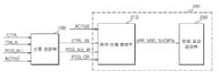
도 4는 본 발명에 따른 반도체 메모리 장치를 나타내는 블록도,4 is a block diagram illustrating a semiconductor memory device according to the present invention;
도 5는 도 4에 도시된 신호 생성부의 내부 회로도,5 is an internal circuit diagram of a signal generator shown in FIG. 4;
도 6은 도 4에 도시된 제어 신호 생성부의 내부 블록도,6 is an internal block diagram of a control signal generation unit shown in FIG. 4;
도 7은 도 6에 도시된 제 1 제어 신호 생성부의 내부 회로도,FIG. 7 is an internal circuit diagram of a first control signal generator shown in FIG. 6;
도 8은 도 6에 도시된 제 2 제어 신호 생성부의 내부 회로도,8 is an internal circuit diagram of a second control signal generator shown in FIG. 6;
도 9는 도 4에 도시된 전압 공급부의 내부 회로도, 및9 is an internal circuit diagram of the voltage supply unit shown in FIG. 4, and
도 10은 본 발명의 반도체 메모리 장치가 로우-패스트(X-Fast) 동작을 하는 경우 액티브-프리차지 방식을 나타내는 타이밍도이다.FIG. 10 is a timing diagram illustrating an active precharge method when a semiconductor memory device of the present invention performs a low-fast operation.
<도면의 주요 부분에 대한 부호 설명><Description of the symbols for the main parts of the drawings>
100 : 신호 생성부200 : 전압 제어부100: signal generator 200: voltage controller
210 : 제어 신호 생성부230 : 전압 공급부210: control signal generator 230: voltage supply unit
211 : 제 1 제어 신호 생성부213 : 제 2 제어 신호 생성부211: first control signal generator 213: second control signal generator
본 발명은 반도체 메모리 장치에 관한 것으로, 보다 상세하게는 제조상 취약한 셀 및 주변 로직에 스트레스(stress)를 가하는 테스트를 수행하여 불량을 미리 발견할 수 있는 반도체 메모리 장치에 관한 것이다.BACKGROUND OF THE
디램(Dynamic Random Access Memory, DRAM)에서 패키지(package) 후에 제품의 불량을 조기 발견하기 위해 동작 전압보다 높은 전압 및 고온에서 번-인 스트레스(Burn-In stress)를 주게 된다. 이는 제조상 취약한 셀들을 미리 스트레스를 가하여 가려내는 작업(Cell B/I) 및 제조상 취약한 주변 로직 부위(peri logic)에 고전압 스트레스를 24 ~ 27 시간 가하여 미리 가려내는 작업이다.In DRAMs (Dynamic Random Access Memory, DRAM), burn-in stresses are applied at high voltages and temperatures above the operating voltage to detect product defects early after package. This is a task of pre-stressing cells that are vulnerable in manufacturing (Cell B / I) and pre-screening by applying high voltage stress 24 to 27 hours to peri-logic that is vulnerable in manufacturing.
번-인 테스트 모드(Burn-In Test Mode)시 높은 전위로 저장된 셀의 스토리지 캐패시터(storage capacitor)의 유전막에 정상 상태 이상의 스트레스를 주어 취약한 셀들을 스크린할 수 있다. 또한 셀 트랜지스터(cell transistor)의 게이트 옥사이드(gate oxide)에 스트레스를 가하기 위하여 일정 전위 이상의 고전압을 인가함으로써 약한 게이트 옥사이드를 파괴하여 스크린(screen) 할 수 있다.In Burn-In Test Mode, vulnerable cells can be screened by stressing the dielectric film of the storage capacitor of the cell stored at a high potential above the normal state. In addition, in order to stress the gate oxide of the cell transistor, a weak gate oxide may be destroyed and screened by applying a high voltage of a predetermined potential or more.
이러한 번-인(Burn-In) 동작을 하기 위해서 디램(DRAM)은 액티브 - 라이트 - 프리차지(Active - Write - Precharge)의 동작 패턴을 가져야 한다. 상기 디램(DRAM)의 동작은 로우-어드레스(X-Address)와 컬럼-어드레스(Y-Address) 스캔 방식에 따라 로우-패스트(X-Fast) 동작과 컬럼-패스트(Y-Fast) 동작으로 나누게 된다.In order to perform this burn-in operation, the DRAM must have an active-write-precharge operation pattern. The operation of the DRAM is divided into a low-speed (X-Fast) operation and a column-fast (Y-Fast) operation according to a low-address (X-Address) and a column-address (Y-Address) scan method. do.
이하, 첨부된 도면을 참조하여 종래의 반도체 메모리 장치를 설명하면 다음과 같다.Hereinafter, a conventional semiconductor memory device will be described with reference to the accompanying drawings.
도 1은 로우-패스트(X-Fast) 동작에 따른 어드레스 진행 방향 및 어드레스 패턴을 나타낸 개념도이며, 도 2는 컬럼-패스트(Y-Fast) 동작에 따른 어드레스 진행 방향 및 어드레스 패턴을 나타낸 개념도이다.FIG. 1 is a conceptual diagram illustrating an address progress direction and an address pattern according to an X-Fast operation, and FIG. 2 is a conceptual diagram illustrating an address progress direction and an address pattern according to a Y-Fast operation.
도 1 및 도 2에 도시된, A0 ~ A(N)은 액티브 명령(Active Command), W0 ~ W(N)은 라이트 명령(Write Command), P0 ~ P(N)은 프리차지 명령(Precharge Command)이다.1 and 2, A0 to A (N) are active commands, W0 to W (N) are write commands, and P0 to P (N) are precharge commands. )to be.
도 1과 도 2를 비교하면 액티브 - 프리차지(Active - Precharge) 하는 횟수가 로우-패스트(X-Fast) 동작의 경우 컬럼-패스트(Y-Fast) 동작에 비해 N배가 많게 되는데 이는 액티브(Active) 또는 프리차지(Precharge) 시에 피크 커런트(peak current)가 많다는 것을 의미한다. 즉, 컬럼-패스트(Y-Fast) 동작의 경우 액티브 - 프리차지(Active - Precharge) 방식은 로우 어드레스를 액티브(Active) 한 후에 컬럼 개수만큼 라이트(Write)를 하고 프리차지(Precharge) 동작을 하기 때문에 워드라인(wordline, 이하 WL) 동작에 따른 피크 커런트(peak current)가 로우-패스트(X-Fast) 동작에 비해 1/N로 감소하게 된다.Compared to FIG. 1 and FIG. 2, the number of active-precharges is N times as high as that of the Y-Fast operation in the case of the X-Fast operation. ) Means that there is a lot of peak current at the time of precharge. That is, in the case of the column-fast operation, the active-precharge method writes as many columns as the number of columns after preactivating the row address and performs the precharge operation. Therefore, the peak current due to the word line (WL) operation is reduced to 1 / N compared to the low-speed (X-Fast) operation.
도 3은 종래의 반도체 메모리 장치가 로우-패스트(X-Fast) 동작을 하는 경우 액티브-프리차지(Active - Precharge) 방식을 나타내는 타이밍도이다.FIG. 3 is a timing diagram illustrating an active precharge method when a conventional semiconductor memory device performs a low-fast operation.
도 3에 도시된 바와 같이 종래의 반도체 메모리 장치는 액티브 명령(Active Command, ACT)이 입력되면, 내부적으로 액티브 신호(ACTIVE)가 발생하게 되고 이 신호에 의해 워드라인(WL)을 고전압(VPP) 레벨까지 상승시키게 된다. 이때, 접지 전압(VSS)으로 디스차지(discharge) 되어 있는 워드라인(WL)을 고전압(VPP) 레벨까지 차지(charge) 해야 하므로 순간적으로 많은 전류를 소모하게 된다.As shown in FIG. 3, in the conventional semiconductor memory device, when an active command (ACT) is input, an active signal ACTIVE is generated internally, and the word line WL is connected to the high voltage VPP by the signal. Will be raised to the level. At this time, since the word line WL discharged to the ground voltage VSS needs to be charged to the high voltage VPP level, a large amount of current is consumed instantaneously.
도 3에 도시된, A는 액티브(Active) 동작시 워드라인(WL)이 동작함에 따른 순간적인 피크 전류(peak current)를 나타내며 B는 프리차지(Precharge) 동작시 발생하는 피크 전류(peak current)를 나타낸 것이다. C는 센스 앰프(Sense Amplifier)가 동작함에 따른 피크 전류(peak current)를 나타낸다.As shown in FIG. 3, A represents an instantaneous peak current according to the operation of the word line WL during the active operation, and B represents the peak current generated during the precharge operation. It is shown. C represents the peak current according to the operation of the sense amplifier.
디램(DRAM)의 용량이 커짐에 따라 동작 전류가 많아지게 되는데 동작 전압보다 높은 외부 전압(VDD)에서 48 ~ 72시간 동안 액티브 - 프리차지(Active - Precharge) 동작을 반복하는 번-인(Burn-In) 테스트의 경우, 로우-패스트(X-Fast) 동작에서 피크 커런트(peak current)가 더 많이 발생하게 된다. 이것은 반도체 메모리 장치에 패키지 볼 멜팅(package ball melting)을 유발하여 패키지 양품률(yield)을 저하시키고 번-인(Burn-In) 소켓(socket)을 손상시킬 수 있어, 생산성 저하가 발생하게 하는 요인이 된다.As the capacity of DRAM increases, the operating current increases, and the burn-in which repeats active-precharge operation for 48 to 72 hours at an external voltage (VDD) higher than the operating voltage. In the case of In) test, there is more peak current in the low-speed (X-Fast) operation. This causes package ball melting in the semiconductor memory device, which can lower the package yield and damage the burn-in sockets, resulting in a decrease in productivity. Becomes
상기 문제를 해결하기 위해 컬럼-패스트(Y-Fast) 동작에 따른 액티브 - 프리차지(Active - Precharge) 방식을 사용하여 피크 커런트(peak current)를 줄이는 방법을 사용할 수 있다. 하지만 컬럼-패스트(Y-Fast) 동작으로 번-인(Burn-In) 테스트를 진행할 때 페리 트랜지스터(peri transistor)의 열화 정도가 약해짐에 따른 스크린 조건이 약해지게 된다.In order to solve the problem, a method of reducing peak current by using an active-precharge method according to a column-fast operation may be used. However, when burn-in test is performed by the column-fast operation, the screen condition is weakened due to the deterioration of the peri transistor.
본 발명은 상술한 문제점을 해결하기 위하여 안출된 것으로, 로우-패스트(X-Fast) 동작에 따라 어드레스를 진행하고, 피크 커런트(peak current)를 분산 시킴으로써 볼 멜팅(ball melting) 문제를 해결하고 번-인(Burn-In) 스트레스(stress)는 기존과 동일하게 줄 수 있는 반도체 메모리 장치를 제공하는데 그 기술적 과제가 있다.
또한, 본 발명은 상기한 반도체 메모리 장치를 이용한 전압 제어방법을 제공하는 데 다른 기술적 과제가 있다.SUMMARY OF THE INVENTION The present invention has been made to solve the above-mentioned problem, and solves the ball melting problem by improving the address according to the low-fast operation and dispersing the peak current. There is a technical problem in providing a semiconductor memory device which can give a burn-in stress in the same manner as the conventional one.
In addition, the present invention has another technical problem to provide a voltage control method using the semiconductor memory device.
상술한 기술적 과제를 달성하기 위한 본 발명의 일 실시예에 따른 반도체 메모리 장치는, 올 뱅크 프리차지 명령에 응답하여 번-인 제어 신호 및 번-인 프리차지 신호를 출력하는 신호 생성 수단; 및 상기 번-인 제어 신호와 상기 번-인 프리차지 신호에 응답하여 제 1 전압 또는 상기 제 1 전압보다 낮은 제 2 전압 중 어느 하나를 워드라인에 공급하는 전압 제어 수단;을 포함한다.In accordance with another aspect of the present invention, a semiconductor memory device includes: signal generation means for outputting a burn-in control signal and a burn-in precharge signal in response to an all-bank precharge command; And voltage control means for supplying one of a first voltage or a second voltage lower than the first voltage to a word line in response to the burn-in control signal and the burn-in precharge signal.
또한 본 발명의 다른 실시예에 따른 반도체 메모리 장치는, 올 뱅크 프리차지 명령에 응답하여 전압 제어 신호를 활성화 시켜 출력하는 제어 신호 생성 수단; 및 액티브 동작 시, 상기 전압 제어 신호에 응답하여, 제 1 전압으로 구동되는 워드라인에 제 2 전압을 인가한 후 상기 제 1 전압이 인가되도록 하고, 프리차지 동작 시, 상기 워드라인이 비활성화 되기 전에 상기 전압 제어 신호에 응답하여 상기 워드라인에 상기 제 2 전압이 인가되도록 하는 전압 공급 제어 수단;을 포함한다.In addition, according to another embodiment of the present invention, a semiconductor memory device includes: control signal generation means for activating and outputting a voltage control signal in response to an all bank precharge command; And in response to the voltage control signal, in response to the voltage control signal, applies the second voltage to the word line driven by the first voltage and then applies the first voltage, and before the word line is deactivated in the precharge operation. Voltage supply control means for applying the second voltage to the word line in response to the voltage control signal.
그리고, 본 발명에 따른 반도체 메모리 장치를 이용한 전압 제어 방법은, a) 번-인 테스트 모드 시, 번-인 테스트 모드 신호를 활성화 시키는 단계; b) 올 뱅크 프리차지 명령에 응답하여, 번-인 제어 신호 및 번-인 프리차지 신호를 활성화 시켜, 전압 제어 신호를 활성화 시키는 단계; c) 액티브 동작 시, 상기 전압 제어 신호에 응답하여, 제 1 전압으로 구동되는 워드라인에 제 2 전압이 인가된 후 상기 제 1 전압이 인가되도록 제어하는 단계; 및 d) 프리차지 동작 시, 상기 워드라인이 비활성화 되기 전에 상기 전압 제어 신호에 응답하여 상기 워드라인에 상기 제 2 전압이 인가되도록 하는 단계;를 포함한다.In addition, the voltage control method using the semiconductor memory device according to the present invention includes the steps of: a) activating the burn-in test mode signal in the burn-in test mode; b) in response to the all bank precharge command, activating the burn-in control signal and the burn-in precharge signal to activate the voltage control signal; c) during the active operation, in response to the voltage control signal, controlling the first voltage to be applied after the second voltage is applied to the word line driven by the first voltage; And d) during the precharge operation, applying the second voltage to the word line in response to the voltage control signal before the word line is deactivated.
이하에서는 첨부된 도면을 참조하여 본 발명의 바람직한 실시예를 보다 상세히 설명하면 다음과 같다.Hereinafter, preferred embodiments of the present invention will be described in detail with reference to the accompanying drawings.
도 4는 본 발명에 따른 반도체 메모리 장치를 나타내는 블록도이다.4 is a block diagram illustrating a semiconductor memory device according to the present invention.
본 발명에 따른 반도체 메모리 장치는 올 뱅크 프리차지 명령(APCG)에 응답하여 번-인 제어 신호(CTRL_BI) 및 번-인 프리차지 신호(PCG_ALL_BI)를 출력하는 신호 생성부(100); 및 상기 번-인 제어 신호(CTRL_BI) 및 상기 번-인 프리차지 신호(PCG_ALL_BI)에 응답하여 제 1 전압(VPP) 또는 상기 제 1 전압(VPP)보다 낮은 제 2 전압(VDD) 중 어느 하나를 워드라인(wordline, 이하, WL)에 공급하는 전압 제어부(200);을 포함한다.According to an exemplary embodiment of the present invention, a semiconductor memory device may include: a
바람직하게는 상기 전압 제어부(200)에 제 1 프리차지 신호(PCG_OR) 및 액티브 신호(ACTIVE)가 추가로 입력되며, 상기 전압 제어부(200)는 상기 제 1 프리차지 신호(PCG_OR), 상기 액티브 신호(ACTIVE), 상기 번-인 제어 신호(CTRL_BI) 및 상기 번-인 프리차지 신호(PCG_ALL_BI)에 응답하여 전압 제어 신호(VPP_VDD_SHORTb)를 출력한다.Preferably, a first precharge signal PCG_OR and an active signal ACTIVE are further input to the
상기 전압 제어부(200)는 상기 액티브 신호(ACTIVE), 상기 제 1 프리차지 신호(PCG_OR), 상기 번-인 프리차지 신호(PCG_ALL_BI) 및 상기 번-인 제어 신호(CTRL_BI)에 응답하여 상기 전압 제어 신호(VPP_VDD_SHORTb)를 출력하는 제어 신호 생성부(210); 및 상기 전압 제어 신호(VPP_VDD_SHORTb)에 응답하여, 상기 제 1 전압(VPP) 및 상기 제 1 전압(VPP)보다 낮은 상기 제 2 전압(VDD) 중 어느 하나를 상기 워드라인(WL)에 공급하는 전압 공급부(230);을 포함한다.The
상기 제 1 프리차지 신호(PCG_OR)는 복수개의 뱅크(BANK) 중 일부를 프리차지(precharge) 시키는 신호이고, 상기 신호 생성부(100)에 입력되는 제 2 프리차지 신호(PCG_ALL)는 복수개의 뱅크 모두를 프리차지(precharge) 시키는 신호인 것을 특징으로 한다.The first precharge signal PCG_OR is a signal for precharging some of the banks BANK, and the second precharge signal PCG_ALL input to the
상기 제 1 프리차지 신호(PCG_OR)는 일반적으로 프리차지 명령(PCG)이 입력되는 경우 활성화 되는 신호이고, 상기 제 2 프리차지 신호(PCG_ALL)는 올 뱅크 프리차지 명령(APCG)이 입력되는 경우 활성화 되는 신호이다.The first precharge signal PCG_OR is generally a signal that is activated when a precharge command PCG is input, and the second precharge signal PCG_ALL is activated when an all bank precharge command APCG is input. Signal.
상기 제 2 전압(VDD)은 외부로부터 공급되는 외부 공급 전압을 예로 들 수 있고, 상기 제 1 전압(VPP)은 상기 제 2 전압(VDD)을 펌핑하여 생성되는 전압을 예로 들 수 있다.For example, the second voltage VDD may be an external supply voltage supplied from the outside, and the first voltage VPP may be a voltage generated by pumping the second voltage VDD.
또한, 신호 생성부(100)에 입력되는 상기 번-인 테스트 모드 신호(TM_BI)는 번-인 테스트 모드(Burn-In Test Mode)시 활성화 되는 신호이고, 상기 제어 신호(CTRL)는 올 뱅크 프리차지 명령(All Bank Precharge Command, APCG)이 입력되는 경우 활성화 되는 신호이며 특정 어드레스를 이용하여 사용할 수 있다.In addition, the burn-in test mode signal TM_BI input to the
도 5는 도 4에 도시된 신호 생성부의 내부 회로도이다.FIG. 5 is an internal circuit diagram of the signal generator shown in FIG. 4.
상기 신호 생성부(100)은 상기 번-인 테스트 모드 신호(TM_BI) 및 상기 제어 신호(CTRL)에 응답하여 상기 번-인 제어 신호(CTRL_BI)를 출력하는 제 1 신호 생성부(110); 및 상기 제 2 프리차지 신호(PCG_ALL)와 상기 액티브 신호(ACTIVE)에 응답하여 상기 번-인 프리차지 신호(PCG_ALL_BI)를 출력하는 제 2 신호 생성부(130);를 포함한다.The
상기 제 1 신호 생성부(110)는 상기 번-인 테스트 모드 신호(TM_BI) 및 상기 제어 신호(CTRL)를 입력받는 제 1 낸드 게이트(ND1); 및 상기 제 1 낸드 게이트(ND1)의 출력 신호를 반전시켜서 상기 번-인 제어 신호(CTRL_BI)로서 출력하는 제 1 인버터(IV1);를 포함한다.The
상기 제 2 신호 생성부(130)는 상기 액티브 신호(ACTIVE)를 반전시키는 제 2 인버터(IV2); 상기 제 2 프리차지 신호(PCG_ALL) 및 상기 제 2 인버터(IV2)의 출력신호를 입력받는 제 2 낸드 게이트(ND2); 및 상기 제 2 낸드 게이트(ND2)의 출력신호를 반전시켜, 상기 번-인 프리차지 신호(PCG_ALL_BI)로서 출력하는 제 3 인버터(IV3);를 포함한다.The
상기 제 1 신호 생성부(110)는 상기 번-인 테스트 모드 신호(TM_BI) 및 상기 제어 신호(CTRL)를 입력받아 앤드(AND) 논리 연산을 하는 논리 소자, 즉 앤드 게이 트(AND gate)로 실시되는 것도 가능함으로 상기 예로 본 발명을 한정하지 않는다.The
도 6은 도 4에 도시된 제어 신호 생성부의 내부 블록도이다.FIG. 6 is an internal block diagram of the control signal generator shown in FIG. 4.
상기 제어 신호 생성부(210)는 액티브 신호(ACTIVE)를 입력받아 상기 액티브 신호(ACTIVE)를 지연시킨 액티브 딜레이 신호(ACTIVE_DEL) 및 상기 액티브 딜레이 신호(ACTIVE_DEL)에 응답하여 펄스 신호인 액티브 딜레이 펄스 신호(ACTIVE_DEL_PUL)를 생성하여 출력하는 제 1 제어 신호 생성부(211); 및 상기 제 1 프리차지 신호(PCG_OR), 상기 번-인 프리차지 신호(PCG_ALL_BI), 상기 번-인 제어 신호(CTRL_BI), 상기 액티브 딜레이 신호(ACTIVE_DEL) 및 상기 액티브 딜레이 펄스 신호(ACTIVE_DEL_PUL)에 응답하여 상기 전압 제어 신호(VPP_VDD_SHORTb)를 생성하는 제 2 제어 신호 생성부(213);를 포함한다.The
도 7은 도 6에 도시된 제 1 제어 신호 생성부의 내부 회로도이다.FIG. 7 is an internal circuit diagram of the first control signal generator illustrated in FIG. 6.
상기 제 1 제어 신호 생성부(211)는 상기 액티브 신호(ACTIVE)를 제 1 시간(td1) 만큼 지연시켜 상기 액티브 딜레이 신호(ACTIVE_DEL)를 출력하는 신호 지연부(211-1); 및 상기 액티브 딜레이 신호(ACTIVE_DEL)에 응답하여 펄스 신호인 상기 액티브 딜레이 펄스 신호(ACTIVE_DEL_PUL)를 출력하는 펄스 발생부(211-3);를 포함한다.The first
상기 신호 지연부(211-1)는, 도시되지는 않았지만, 예를 들어 복수개의 인버터를 구비하여 실시하는 것이 가능하다.Although not shown, the signal delay unit 211-1 can be implemented with a plurality of inverters, for example.
상기 펄스 발생부(211-3)는 상기 액티브 딜레이 신호(ACTIVE_DEL)를 제 2 시간(td2) 만큼 반전 지연시키는 반전 지연부(211-31); 상기 액티브 딜레이 신호(ACTIVE_DEL) 및 상기 반전 지연부(211-31)의 출력 신호를 입력받는 제 3 낸드 게이트(ND3); 및 상기 제 3 낸드 게이트(ND3)의 출력신호를 입력받아 상기 액티브 딜레이 펄스 신호(ACTIVE_DEL_PUL)를 출력하는 제 4 인버터(IV4);를 포함한다.The pulse generator 211-3 may include an inversion delay unit 211-31 for inverting and delaying the active delay signal ACTIVE_DEL by a second time td2. A third NAND gate ND3 receiving the active delay signal ACTIVE_DEL and the output signal of the inversion delay units 211-31; And a fourth inverter IV4 that receives the output signal of the third NAND gate ND3 and outputs the active delay pulse signal ACTIVE_DEL_PUL.
본 발명에서는 상기 펄스 발생부(211-3)를 낸드 게이트 및 인버터를 구비하여 실시하였지만, 설계자의 의도에 따라 다른 논리 소자를 사용하여 펄스 신호를 생성하는 것도 가능함으로 상기 실시예에 본 발명을 한정하지 않음을 밝혀둔다.In the present invention, the pulse generator 211-3 is provided with a NAND gate and an inverter, but the present invention is limited to the above embodiment by generating a pulse signal using another logic element according to a designer's intention. Make sure you don't.
도 8은 도 6에 도시된 제 2 제어 신호 생성부의 내부 회로도이다.FIG. 8 is an internal circuit diagram of the second control signal generator shown in FIG. 6.
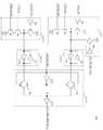
상기 제 2 제어 신호 생성부(213)는 상기 제 1 프리차지 신호(PCG_OR), 상기 번-인 제어 신호(CTRL_BI), 상기 액티브 딜레이 신호(ACTIVE_DEL) 및 상기 액티브 딜레이 펄스 신호(ACTIVE_DEL_PUL)에 응답하여 제 1 노드(S1)의 전위를 변화시키는 제 1 신호 입력부(213-1); 상기 제 1 노드(S1)의 전위를 래치(latch)하는 제 1 래치부(213-2); 상기 번-인 프리차지 신호(PCG_ALL_BI), 상기 번-인 제어 신호(CTRL_BI) 및 상기 액티브 딜레이 신호(ACTIVE_DEL)에 응답하여 제 2 노드(S2)의 전위를 변화시키는 제 2 신호 입력부(213-3); 상기 제 2 노드(S2)의 전위를 래치하는 제 2 래치부(213-4); 상기 액티브 딜레이 신호(ACTIVE_DEL)에 응답하여, 상기 제 1 래치부(213-2) 및 상기 제 2 래치부(213-4)의 출력 신호 중 어느 하나를 구동시켜 상기 전압 제어 신호(VPP_VDD_SHORTb)로서 출력하는 신호 구동부(213-5);를 포함한다.The second
상기 제 1 신호 입력부(213-1)는 상기 제 1 프리차지 신호(PCG_OR)를 입력받는 제 5 인버터(IV5); 게이트 단이 상기 제 5 인버터(IV5)의 출력 단에 연결되고 소스 단이 상기 제 2 전압(VDD)을 인가받으며 드레인 단이 상기 제 1 노드(S1)에 연결되는 제 1 트랜지스터(P1); 게이트 단이 상기 번-인 제어 신호(CTRL_BI)를 입력받고 드레인 단이 상기 제 1 노드(S1)에 연결되는 제 2 트랜지스터(N1); 게이트 단이 상기 액티브 딜레이 신호(ACTIVE_DEL)를 입력받고 드레인 단이 상기 제 2 트랜지스터(N1)의 소스 단과 연결되며 소스 단이 접지 전압(VSS)을 인가받는 제 3 트랜지스터(N2); 상기 액티브 딜레이 펄스 신호(ACTIVE_DEL_PUL)를 입력받는 제 6 인버터(IV6); 및 게이트 단이 상기 제 6 인버터(IV6)의 출력 단과 연결되고 소스 단이 상기 제 2 전압(VDD)을 인가받으며 드레인 단이 상기 제 1 노드(S1)에 연결된 제 4 트랜지스터(P1);를 포함한다.The first signal input unit 213-1 may include a fifth inverter IV5 receiving the first precharge signal PCG_OR; A first transistor P1 having a gate terminal connected to an output terminal of the fifth inverter IV5, a source terminal receiving the second voltage VDD, and a drain terminal connected to the first node S1; A second transistor (N1) having a gate terminal input to the burn-in control signal (CTRL_BI) and a drain terminal connected to the first node (S1); A third transistor N2 of which a gate terminal receives the active delay signal ACTIVE_DEL, a drain terminal is connected to a source terminal of the second transistor N1, and a source terminal receives a ground voltage VSS; A sixth inverter IV6 receiving the active delay pulse signal ACTIVE_DEL_PUL; And a fourth transistor P1 having a gate terminal connected to an output terminal of the sixth inverter IV6, a source terminal receiving the second voltage VDD, and a drain terminal connected to the first node S1. do.
상기 제 1 래치부(213-2)는 상기 제 1 노드(S1)에 연결되어 상기 제 1 노드(S1)의 전위를 반전시키는 제 7 인버터(IV7); 및 상기 제 7 인버터(IV7)의 출력신호를 반전시켜 이를 상기 제 1 노드(S1)에 제공하는 제 8 인버터(IV8);를 포함한다.The first latch unit 213-2 may include a seventh inverter IV7 connected to the first node S1 to invert a potential of the first node S1; And an eighth inverter IV8 inverting the output signal of the seventh inverter IV7 and providing the same to the first node S1.
상기 제 2 신호 입력부(213-3)는 상기 액티브 딜레이 신호(ACTIVE_DEL)를 입력받는 제 9 인버터(IV9); 게이트 단이 상기 제 9 인버터(IV9)의 출력 단에 연결되고 소스 단이 상기 제 2 전압(VDD)을 인가받으며 드레인 단이 상기 제 2 노드(S2)에 연결되는 제 5 트랜지스터(P3); 게이트 단이 상기 번-인 제어 신호(CTRL_BI)를 입력받고 드레인 단이 상기 제 2 노드(S2)에 연결되는 제 6 트랜지스터(N3); 게이트 단이 상기 번-인 프리차지 신호(PCG_ALL_BI)를 입력받고 드레인 단이 상기 제 6 트랜지스터(N3)의 소스 단에 연결되며 소스 단이 상기 접지 전압(VSS)을 인가받는 제 7 트랜지스터(N4);를 포함한다.The second signal input unit 213-3 may include a ninth inverter IV9 receiving the active delay signal ACTIVE_DEL; A fifth transistor (P3) having a gate terminal connected to an output terminal of the ninth inverter (IV9), a source terminal receiving the second voltage (VDD), and a drain terminal connected to the second node (S2); A sixth transistor (N3) having a gate terminal thereof receiving the burn-in control signal (CTRL_BI) and a drain terminal thereof being connected to the second node (S2); A seventh transistor N4 of which a gate terminal receives the burn-in precharge signal PCG_ALL_BI, a drain terminal is connected to a source terminal of the sixth transistor N3, and a source terminal is applied the ground voltage VSS. It includes;
상기 제 2 래치부(213-4)는 상기 제 2 노드(S2)와 연결되어 상기 제 2 노드(S2)의 전위를 반전시키는 제 10 인버터(IV10); 및 상기 제 10 인버터(IV10)의 출력신호를 반전시켜 이를 상기 제 2 노드(S2)에 제공하는 제 11 인버터(IV11);를 포함한다.The second latch unit 213-4 may include a tenth inverter IV10 connected to the second node S2 to invert a potential of the second node S2; And an eleventh inverter IV11 inverting the output signal of the tenth inverter IV10 and providing the same to the second node S2.
상기 신호 구동부(213-5)는 상기 액티브 딜레이 신호(ACTIVE_DEL)를 반전 구동시키는 제 12 인버터(IV12); 상기 액티브 딜레이 신호(ACTIVE_DEL)에 응답하여 상기 제 1 래치부(213-2)의 출력 신호를 제 3 노드(S3)에 출력할지를 결정하는 제 1 스위칭 소자(PG1); 상기 액티브 딜레이 신호(ACTIVE_DEL)에 응답하여 상기 제 2 래치부(213-4)의 출력 신호를 상기 제 3 노드(S3)에 출력할지를 결정하는 제 2 스위칭 소자(PG2); 및 상기 제 3 노드(S3)의 신호를 반전 구동시켜 상기 전압 제어 신호(VPP_VDD_SHORTb)를 출력하는 제 13 인버터(IV13);를 포함한다.The signal driver 213-5 may include a twelfth inverter IV12 for inverting the active delay signal ACTIVE_DEL; A first switching device (PG1) determining whether to output the output signal of the first latch unit (213-2) to a third node (S3) in response to the active delay signal (ACTIVE_DEL); A second switching element (PG2) which determines whether to output the output signal of the second latch unit (213-4) to the third node (S3) in response to the active delay signal (ACTIVE_DEL); And a thirteenth inverter IV13 outputting the voltage control signal VPP_VDD_SHORTb by inverting the signal of the third node S3.
본 발명에서는 상기 제 1 스위칭 소자(PG1) 및 상기 제 2 스위칭 소자(PG2)는 패스 게이트로 실시 되었으며, 상기 제 1 트랜지스터(P1), 상기 제 4 트랜지스터(P2) 및 상기 제 5 트랜지스터(P3)는 피모스(PMOS) 트랜지스터이고, 상기 제 2 트랜지스터(N1), 상기 제 3 트랜지스터(N2), 상기 제 6 트랜지스터(N3) 및 상기 제 7 트랜지스터(N4)는 엔모스(NMOS) 트랜지스터로 실시 되었다.In the present invention, the first switching element PG1 and the second switching element PG2 are implemented as pass gates, and the first transistor P1, the fourth transistor P2, and the fifth transistor P3. Is a PMOS transistor, and the second transistor N1, the third transistor N2, the sixth transistor N3, and the seventh transistor N4 are implemented as an NMOS transistor. .
도 9는 도 4에 도시된 전압 공급부의 내부 회로도이다.FIG. 9 is an internal circuit diagram of the voltage supply unit shown in FIG. 4.
상기 전압 공급부(230)는 상기 전압 제어 신호(VPP_VDD_SHORTb)에 응답하여 상기 제 1 전압(VPP) 및 상기 제 2 전압(VDD)을 쇼트(short)시키는 제 8 트랜지스터(P4)를 포함하며, 상기 제 8 트랜지스터(P4)는 상기 전압 제어 신 호(VPP_VDD_SHORTb)에 응답하여 상기 제 1 전압(VPP) 및 상기 제 2 전압(VDD)을 쇼트(short)시키는 스위칭 소자로 대체하여 실시하는 것도 가능하다.The
상기 전압 공급부(230)는 설계자의 의도에 따라 상기 실시예와 다른 방식으로 상기 전압 제어 신호(VPP_VDD_SHORTb)에 응답하여 상기 워드라인(WL)에 상기 제 1 전압(VPP) 및 상기 제 2 전압(VDD) 중 어느 하나를 공급하도록 설계가 가능함으로 상기 실시예로 본 발명을 한정하지 않음을 밝혀둔다.The
도 10은 본 발명의 반도체 메모리 장치가 로우-패스트(X-Fast) 동작을 하는 경우 액티브-프리차지 방식을 나타내는 타이밍도이다.FIG. 10 is a timing diagram illustrating an active precharge method when a semiconductor memory device of the present invention performs a low-fast operation.
본 발명에 따른 반도체 메모리 장치의 동작을 도 4 내지 도 10을 참조하여 설명하면 다음과 같다.An operation of the semiconductor memory device according to the present invention will be described with reference to FIGS. 4 through 10.
본 발명에 따른 반도체 메모리 장치는 번-인 테스트 모드(Burn-In Test Mode) 진입 후에 원하는 전압 레벨에 각 파워(power)가 안정화된 후 액티브 하기 전에 올 뱅크 프리차지 명령(APCG)이 입력되면, 더미 올 뱅크 프리차지(Dummy All Bank Precharge) 동작을 한번 수행한다. 상기 올 뱅크 프리차지 동작은 반도체 메모리에 있어서 프리차지(precharge)를 한번 더 하는 것이므로 정상적인 동작에 영향을 미치지 않는다. 상기 올 뱅크 프리차지 동작에서 상기 제어 신호(CTRL)는 활성화 된 펄스 신호이므로, 상기 신호 생성부(100)에서 활성화된 펄스 신호인 상기 번-인 제어 신호(CTRL_BI)로 나타내어 진다.In the semiconductor memory device according to the present invention, when the all-bank precharge command APCG is input before the power is stabilized at the desired voltage level after the burn-in test mode is entered, the power is stabilized. Dummy All Bank Precharge is performed once. Since the all bank precharge operation is to precharge the semiconductor memory once more, it does not affect the normal operation. Since the control signal CTRL is an activated pulse signal in the all bank precharge operation, the control signal CTRL is represented by the burn-in control signal CTRL_BI, which is a pulse signal activated by the
상기 올 뱅크 프리차지 명령(APCG)이 인가되는 경우 상기 제 2 프리차지 신호(PCG_ALL)는 하이 레벨로 활성화 되는 펄스 신호이고, 상기 제 1 프리차지 신 호(PCG_OR)는 로우 레벨 상태를 유지하며, 프리차지 명령(PCG)이 입력되면 상기 제 1 프리차지 신호(PCG_OR)는 하이 레벨로 활성화 되는 펄스 신호이고, 상기 제 2 프리차지 신호(PCG_ALL)는 로우 레벨 상태를 유지한다.When the all bank precharge command APCG is applied, the second precharge signal PCG_ALL is a pulse signal activated to a high level, and the first precharge signal PCG_OR maintains a low level state. When the precharge command PCG is input, the first precharge signal PCG_OR is a pulse signal that is activated at a high level, and the second precharge signal PCG_ALL maintains a low level.
상기 액티브 신호(ACTIVE)가 로우 레벨인 상태에서, 상기 올 뱅크 프리차지 명령(APCG)이 인가되는 경우, 상기 제 1 프리차지 신호(PCG_OR)는 로우 레벨을 유지하고, 상기 액티브 딜레이 신호(ACTIVE_DEL) 및 상기 액티브 딜레이 펄스 신호(ACTIVE_DEL_PUL)도 로우 레벨을 유지한다. 하지만, 상기 제 2 프리차지 신호(PCG_ALL) 및 상기 번-인 제어 신호(CTRL_BI)는 하이 레벨로 활성화 되므로, 상기 제 2 신호 생성부(130)는 하이 레벨의 상기 번-인 프리차지 신호(PCG_ALL_BI)를 출력한다.When the all bank precharge command APCG is applied while the active signal ACTIVE is at the low level, the first precharge signal PCG_OR is maintained at the low level and the active delay signal ACTIVE_DEL. And the active delay pulse signal ACTIVE_DEL_PUL also maintains a low level. However, since the second precharge signal PCG_ALL and the burn-in control signal CTRL_BI are activated at a high level, the
도 8에 도시된 상기 제 2 제어 신호 생성부(213)를 참조하면, 상기 번-인 제어 신호(CTRL_BI) 및 상기 번-인 프리차지 신호(PCG_ALL_BI)에 각각 응답하여 상기 제 6 트랜지스터(N3) 및 상기 제 7 트랜지스터(N4)가 턴-온(turn-on) 되어 상기 제 2 노드(S2)의 전위는 로우 레벨로 천이 되고, 상기 제 2 래치부(213-4)는 상기 제 2 노드(S2)의 전위를 로우 레벨로 유지한다. 이때, 상기 액티브 딜레이 신호(ACTIVE_DEL)가 로우 레벨이므로 상기 제 2 패스 게이트(PG2)가 턴-온(turn-on) 되어 상기 제 3 노드(S3)의 전위는 하이 레벨이 되고, 상기 전압 제어 신호(VPP_VDD_SHORTb)는 로우 레벨로 천이한다. 상기 전압 제어 신호(VPP_VDD_SHORTb)에 응답하여 상기 전압 공급부(230)는 상기 제 1 전압(VPP)과 상기 제 2 전압(VDD)을 쇼트(short)시켜 상기 제 1 전압(VPP)을 상기 제 2 전압(VDD)으로 다운시킨다.Referring to the second
이후, 액티브 명령(ACT)이 입력되는 경우, 상기 액티브 신호(ACTIVE)는 하이 레벨로 활성화 되고, 상기 액티브 신호(ACTIVE)가 상기 신호 지연부(211-1)에서 상기 제 1 시간(td1) 만큼 지연되어 상기 액티브 딜레이 신호(ACTIVE_DEL)로 출력되며, 상기 펄스 발생부(211-3)에서 상기 액티브 딜레이 신호(ACTIVE_DEL)를 입력받아 상기 제 2 시간 만큼(td2)의 활성화 구간을 가지는 펄스 신호인 상기 액티브 딜레이 펄스 신호(ACTIVE_DEL_PUL)를 출력한다.Thereafter, when the active command ACT is input, the active signal ACTIVE is activated to a high level, and the active signal ACTIVE is activated by the signal delay unit 211-1 for the first time td1. The pulse signal is delayed and output as the active delay signal ACTIVE_DEL. The pulse generator 211-3 receives the active delay signal ACTIVE_DEL as a pulse signal having an activation period of td2 for the second time. The active delay pulse signal ACTIVE_DEL_PUL is output.
상기 액티브 신호(ACTIVE)에 응답하여 상기 워드라인(WL)이 활성화 되고, 상기 워드라인(WL)의 전위는 상기 제 1 지연 시간(td1) 동안 상기 제 2 전압(VDD)으로 상승하고, 상기 액티브 딜레이 펄스 신호(ACTIVE_DEL_PUL)에 응답하여, 상기 제 2 지연 시간(td2) 동안 상기 제 1 전압(VPP)으로 상승한다. 즉, 상기 전압 제어 신호(VPP_VDD_SHORTb)가 로우 레벨인 구간에서 상기 액티브 신호(ACTIVE)가 활성화 되면, 상기 제 1 지연 시간(td1) 동안 상기 워드라인(WL)은 상기 제 2 전압(VDD)을 인가받아 상기 제 2 전압(VDD)으로 상승하며, 이후 상기 액티브 딜레이 펄스 신호(ACTIVE_DEL_PUL)가 활성화 되는 구간에서 상기 전압 제어 신호(VPP_VDD_SHORTb)가 하이 레벨로 천이 되므로 상기 제 2 지연 시간(td2) 동안 상기 워드라인(WL)의 전위는 상기 제 1 전압(VPP)으로 상승한다.In response to the active signal ACTIVE, the word line WL is activated, the potential of the word line WL rises to the second voltage VDD during the first delay time td1, and the active In response to the delay pulse signal ACTIVE_DEL_PUL, the voltage rises to the first voltage VPP during the second delay time td2. That is, when the active signal ACTIVE is activated in the period where the voltage control signal VPP_VDD_SHORTb is at a low level, the word line WL applies the second voltage VDD during the first delay time td1. The voltage control signal VPP_VDD_SHORTb transitions to a high level in a period in which the active delay pulse signal ACTIVE_DEL_PUL is activated, and then the word is raised during the second delay time td2. The potential of the line WL rises to the first voltage VPP.
도 8을 참조하여 상세히 설명하면, 상기 액티브 딜레이 펄스 신호(ACTIVE_DEL_PUL)가 하이 레벨로 활성화되는 구간에서 상기 제 4 트랜지스터(P2)가 턴-온(turn-on) 되어 상기 제 1 노드(S1)는 하이 레벨로 천이되고, 상기 제 1 래치부(213-2)는 상기 제 1 노드(S1)를 하이 레벨로 유지한다. 상기 액티브 딜레이 신호(ACTIVE_DEL)가 하이 레벨 상태이므로 상기 제 1 패스 게이트(PG1)가 턴-온(turn-on) 되어 상기 제 3 노드(S3)는 로우 레벨을 유지한다. 즉, 상기 전압 제어 신호(VPP_VDD_SHORTb)는 하이 레벨로 천이 된다.In detail, referring to FIG. 8, the fourth transistor P2 is turned on in the period in which the active delay pulse signal ACTIVE_DEL_PUL is activated at a high level, so that the first node S1 is turned on. Transitioning to the high level, the first latch unit 213-2 maintains the first node (S1) at a high level. Since the active delay signal ACTIVE_DEL is in a high level state, the first pass gate PG1 is turned on so that the third node S3 maintains a low level. That is, the voltage control signal VPP_VDD_SHORTb transitions to a high level.
이후, 상기 프리차지 명령(PCG) 전에 상기 올 뱅크 프리차지 명령(APCG)에 의해 상기 제어 신호(CTRL)가 더미(dummy)로 활성화 되는 펄스를 가지게 되면 상기 제 1 신호 생성부(110)에서 하이 레벨로 활성화 되는 펄스 신호인 상기 번-인 제어 신호(CTRL_BI)를 출력하고, 상기 제 2 제어 신호 생성부(130)에서 로우 레벨의 상기 번-인 프리차지 신호(PCG_ALL_BI)를 출력한다. 번-인 테스트 모드(Burn-In Test Mode)에서 상기 제어 신호(CTRL)가 더미(dummy)로 활성화 되는 펄스를 갖는 경우 디램(DRAM)의 정상 동작에 문제가 없다. 예를 들어, D와 같이 번-인 테스트 모드(Burn-In Test Mode)가 아닐 경우 상기 신호 생성부(100)는 로우 레벨의 상기 번-인 테스트 모드 신호(TM_BI)와 하이 레벨의 상기 제어 신호(CTRL)를 입력받게 되어 E와 같이 로우 레벨의 상기 번-인 제어 신호(CTRL_BI)를 출력한다.Subsequently, when the control signal CTRL is activated as a dummy by the all-bank precharge command APCG before the precharge command PCG, the
이때, 상기 번-인 제어 신호(CTRL_BI) 및 상기 액티브 딜레이 신호(ACTIVE_DEL)에 응답하여 상기 제 2 트랜지스터(N1) 및 상기 제 3 트랜지스터(N2)가 턴-온(turn-on) 되어 상기 제 1 노드(S1)는 로우 레벨로 천이 되고, 상기 제 1 래치부(213-2)는 상기 제 1 노드(S1)의 전위를 로우 레벨을 유지한다. 하이 레벨의 상기 액티브 딜레이 신호(ACTIVE_DEL)에 응답하여 상기 제 1 패스 게이트(PG1)가 턴-온(turn-on) 되어 상기 제 3 노드(S3)는 하이 레벨로 유지되고, 상기 제 13 인버터(IV13)에 의해 상기 전압 제어 신호(VPP_VDD_SHORTb)는 로우 레벨로 천이 된다. 상기 전압 제어 신호(VPP_VDD_SHORTb)에 응답하여 상기 전압 공급부(230)가 상기 제 1 전압(VPP)과 상기 제 2 전압(VDD)을 쇼트 시키므로 상기 워드라인(WL)의 전위는 상기 제 2 전압(VDD)으로 다운된다. 이후, 상기 프리차지 명령(PCG)이 입력되면 상기 액티브 신호(ACTIVE)는 비활성화 되고, 상기 액티브 신호(ACTIVE)에 응답하여 상기 워드라인(WL)이 상기 접지 전압(VSS)으로 다운되게 된다. 상기 프리차지 명령(PCG)이 입력될 때, 상기 제 1 프리차지 신호(PCG_OR)가 하이 레벨로 활성화 되는 펄스 신호를 가지므로 상기 제 1 트랜지스터(P1)가 턴-온(turn-on) 되어 상기 제 1 노드(S1)의 전위는 하이 레벨로 천이 되며, 상기 제 1 래치부(213-2)는 상기 제 1 노드(S1)의 전위를 하이 레벨로 유지한다. 이때, 상기 액티브 딜레이 신호(ACTIVE_DEL)가 하이 레벨을 유지하고 있으므로 상기 제 1 패스 게이트(PG1)가 턴-온(turn-on) 되어 상기 제 3 노드(S3)의 전위는 로우 레벨로 천이 된다. 즉, 상기 전압 제어 신호(VPP_VDD_SHORTb)가 하이 레벨로 천이 된다.In this case, the second transistor N1 and the third transistor N2 are turned on in response to the burn-in control signal CTRL_BI and the active delay signal ACTIVE_DEL, so that the first transistor is turned on. The node S1 transitions to a low level, and the first latch unit 213-2 maintains the potential of the first node S1 at a low level. In response to the active delay signal ACTIVE_DEL having a high level, the first pass gate PG1 is turned on so that the third node S3 is maintained at a high level and the thirteenth inverter ( IV13), the voltage control signal VPP_VDD_SHORTb transitions to a low level. The
상기 설명한 바와 같이, 본 발명에 따른 반도체 메모리 장치는 액티브 동작시 상기 워드라인(WL)을 구동할 때, 상기 제 2 전압(VDD)으로 상기 워드라인(WL)의 전위를 높인 이후 상기 제 2 전압(VDD)보다 높은 상기 제 1 전압(VPP)으로 상기 워드라인(WL)을 구동 시킴으로써, 피크 전류(peak current)를 분산시킬 수 있다. 또한 프리차지(Precharge) 동작시, 상기 프리차지 동작 이전에 상기 워드라인(WL)의 전위를 상기 제 2 전압(VDD)으로 낮추고, 이후 상기 접지 전압(VSS)으로 낮춤으로써 피크 전류(peak current)를 분산시킬 수 있다.As described above, in the semiconductor memory device according to the present invention, when the word line WL is driven during an active operation, the second voltage is increased after the potential of the word line WL is increased to the second voltage VDD. The peak current may be dispersed by driving the word line WL with the first voltage VPP higher than VDD. In the precharge operation, the current of the word line WL is lowered to the second voltage VDD before the precharge operation, and then the voltage is lowered to the ground voltage VSS. Can be dispersed.
도 10에 도시된 바와 같이, F는 액티브 동작시 피크 전류가 분산되는 것을 보여주며, G는 프리차지 동작시 피크 전류가 분산되는 것을 보여준다.As shown in FIG. 10, F shows that the peak current is dispersed during the active operation, and G shows that the peak current is dispersed during the precharge operation.
이와 같이, 본 발명이 속하는 기술분야의 당업자는 본 발명이 그 기술적 사상이나 필수적 특징을 변경하지 않고서 다른 구체적인 형태로 실시될 수 있다는 것을 이해할 수 있을 것이다. 그러므로 이상에서 기술한 실시예들은 모든 면에서 예시적인 것이며 한정적인 것이 아닌 것으로서 이해해야만 한다. 본 발명의 범위는 상기 상세한 설명보다는 후술하는 특허청구범위에 의하여 나타내어지며, 특허청구범위의 의미 및 범위 그리고 그 등가개념으로부터 도출되는 모든 변경 또는 변형된 형태가 본 발명의 범위에 포함되는 것으로 해석되어야 한다.As such, those skilled in the art will appreciate that the present invention can be implemented in other specific forms without changing the technical spirit or essential features thereof. Therefore, the above-described embodiments are to be understood as illustrative in all respects and not as restrictive. The scope of the present invention is shown by the following claims rather than the detailed description, and all changes or modifications derived from the meaning and scope of the claims and their equivalents should be construed as being included in the scope of the present invention. do.
본 발명에 따른 반도체 메모리 장치는 액티브 동작 및 프리차지 동작시에 발생하는 피크 전류(peak current)를 분산 시킴으로써 과도한 피크 전류에 의한 패키지 볼 멜팅(Package Ball Melting)을 방지를 할 수 있어 반도체 메모리의 생산성 향상 및 번-인 스크린 능력 향상의 효과를 수반한다.The semiconductor memory device according to the present invention can prevent package ball melting due to excessive peak current by dispersing peak current generated during active and precharge operations, thereby improving productivity of semiconductor memory. Entails the effect of enhancement and burn-in screen capability enhancement.
Claims (48)
Translated fromKoreanPriority Applications (4)
| Application Number | Priority Date | Filing Date | Title |
|---|---|---|---|
| KR1020060099652AKR100845774B1 (en) | 2006-10-13 | 2006-10-13 | Semiconductor memory device and voltage control method using same |
| US11/822,358US7502268B2 (en) | 2006-10-13 | 2007-07-05 | Voltage control apparatus and method of controlling voltage using the same |
| JP2007214164AJP2008097804A (en) | 2006-10-13 | 2007-08-20 | Voltage controller and control method |
| US12/364,670US7916566B2 (en) | 2006-10-13 | 2009-02-03 | Voltage control apparatus and method of controlling voltage using the same |
Applications Claiming Priority (1)
| Application Number | Priority Date | Filing Date | Title |
|---|---|---|---|
| KR1020060099652AKR100845774B1 (en) | 2006-10-13 | 2006-10-13 | Semiconductor memory device and voltage control method using same |
Publications (2)
| Publication Number | Publication Date |
|---|---|
| KR20080033683A KR20080033683A (en) | 2008-04-17 |
| KR100845774B1true KR100845774B1 (en) | 2008-07-14 |
Family
ID=39302947
Family Applications (1)
| Application Number | Title | Priority Date | Filing Date |
|---|---|---|---|
| KR1020060099652AExpired - Fee RelatedKR100845774B1 (en) | 2006-10-13 | 2006-10-13 | Semiconductor memory device and voltage control method using same |
Country Status (3)
| Country | Link |
|---|---|
| US (2) | US7502268B2 (en) |
| JP (1) | JP2008097804A (en) |
| KR (1) | KR100845774B1 (en) |
Families Citing this family (4)
| Publication number | Priority date | Publication date | Assignee | Title |
|---|---|---|---|---|
| KR100845776B1 (en)* | 2006-11-23 | 2008-07-14 | 주식회사 하이닉스반도체 | Sense Amplifier Control Circuit and Method of Semiconductor Memory Device |
| KR100955682B1 (en)* | 2008-04-28 | 2010-05-03 | 주식회사 하이닉스반도체 | Sensing Delay Circuit and Semiconductor Memory Device Using the Same |
| KR101539402B1 (en)* | 2008-10-23 | 2015-07-27 | 삼성전자주식회사 | Semiconductor Package |
| KR101047003B1 (en)* | 2009-06-26 | 2011-07-06 | 주식회사 하이닉스반도체 | Precharge signal generation circuit and semiconductor memory device |
Family Cites Families (21)
| Publication number | Priority date | Publication date | Assignee | Title |
|---|---|---|---|---|
| JPH07105144B2 (en)* | 1985-05-20 | 1995-11-13 | 富士通株式会社 | Semiconductor memory circuit |
| JPS62228177A (en)* | 1986-03-29 | 1987-10-07 | Toshiba Corp | Tolerant input voltage inspection circuit for semiconductor integrated circuit |
| US5402375A (en)* | 1987-11-24 | 1995-03-28 | Hitachi, Ltd | Voltage converter arrangement for a semiconductor memory |
| JPH01162296A (en)* | 1987-12-19 | 1989-06-26 | Sony Corp | Dram |
| JP2737293B2 (en)* | 1989-08-30 | 1998-04-08 | 日本電気株式会社 | MOS type semiconductor memory device |
| JP2821278B2 (en)* | 1991-04-15 | 1998-11-05 | 日本電気アイシーマイコンシステム株式会社 | Semiconductor integrated circuit |
| KR0119887B1 (en)* | 1994-06-08 | 1997-10-30 | 김광호 | Wafer Burn-in Test Circuit of Semiconductor Memory Device |
| US5901105A (en)* | 1995-04-05 | 1999-05-04 | Ong; Adrian E | Dynamic random access memory having decoding circuitry for partial memory blocks |
| JP3607760B2 (en) | 1995-10-13 | 2005-01-05 | 富士通株式会社 | Semiconductor integrated circuit device |
| JPH10106257A (en)* | 1996-09-06 | 1998-04-24 | Texas Instr Inc <Ti> | Integrated circuit memory, and method for imparting precharge operation |
| JP3742191B2 (en)* | 1997-06-06 | 2006-02-01 | 株式会社東芝 | Semiconductor integrated circuit device |
| JP4090570B2 (en)* | 1998-06-02 | 2008-05-28 | 株式会社ルネサステクノロジ | Semiconductor device, data processing system, and nonvolatile memory cell threshold value changing method |
| KR100281693B1 (en)* | 1998-09-02 | 2001-02-15 | 윤종용 | High speed three phase booster circuit |
| JP3863313B2 (en)* | 1999-03-19 | 2006-12-27 | 富士通株式会社 | Semiconductor memory device |
| JP4555416B2 (en)* | 1999-09-22 | 2010-09-29 | 富士通セミコンダクター株式会社 | Semiconductor integrated circuit and control method thereof |
| US6563746B2 (en)* | 1999-11-09 | 2003-05-13 | Fujitsu Limited | Circuit for entering/exiting semiconductor memory device into/from low power consumption mode and method of controlling internal circuit at low power consumption mode |
| KR100333710B1 (en)* | 1999-12-28 | 2002-04-22 | 박종섭 | DDR SDRAM for stable read operation |
| JP3856424B2 (en)* | 2000-12-25 | 2006-12-13 | 株式会社東芝 | Semiconductor memory device |
| JP2002231000A (en)* | 2001-02-05 | 2002-08-16 | Mitsubishi Electric Corp | Semiconductor storage device |
| KR100505702B1 (en) | 2003-08-20 | 2005-08-02 | 삼성전자주식회사 | Repair apparatus of semiconductor memory device capable of selectively programming in wafer test and in post package test and repair method of the same |
| KR100586555B1 (en)* | 2005-01-17 | 2006-06-08 | 주식회사 하이닉스반도체 | Internal voltage generation control circuit and internal voltage generation circuit using the same |
- 2006
- 2006-10-13KRKR1020060099652Apatent/KR100845774B1/ennot_activeExpired - Fee Related
- 2007
- 2007-07-05USUS11/822,358patent/US7502268B2/enactiveActive
- 2007-08-20JPJP2007214164Apatent/JP2008097804A/enactivePending
- 2009
- 2009-02-03USUS12/364,670patent/US7916566B2/enactiveActive
Non-Patent Citations (1)
| Title |
|---|
| "DEEP POWER DOWN", Technical Note No. E0598E21, Elpida Memory Inc., 2006. (2006년 5월 공개) |
Also Published As
| Publication number | Publication date |
|---|---|
| US7502268B2 (en) | 2009-03-10 |
| JP2008097804A (en) | 2008-04-24 |
| US20090141572A1 (en) | 2009-06-04 |
| KR20080033683A (en) | 2008-04-17 |
| US20080089148A1 (en) | 2008-04-17 |
| US7916566B2 (en) | 2011-03-29 |
Similar Documents
| Publication | Publication Date | Title |
|---|---|---|
| US10790000B2 (en) | Apparatuses and method for reducing row address to column address delay | |
| US20200027490A1 (en) | Apparatuses and methods for reducing row address to column address delay | |
| US8320210B2 (en) | Memory circuit and a tracking circuit thereof | |
| JP2007012244A (en) | Latency control circuit for semiconductor memory device | |
| US6236605B1 (en) | Semiconductor integrated circuit and semiconductor memory device including overdriving sense amplifier | |
| JP5119795B2 (en) | Semiconductor memory, semiconductor memory test method and system | |
| KR20150080261A (en) | Active control device and semiconductor device including the same | |
| KR100845774B1 (en) | Semiconductor memory device and voltage control method using same | |
| US20190392877A1 (en) | Apparatuses and method for reducing row address to column address delay | |
| US6894942B2 (en) | Refresh control circuit and method for semiconductor memory device | |
| JP5073181B2 (en) | Semiconductor memory device leakage current control device | |
| US6233183B1 (en) | Semiconductor memory device with high data access speed | |
| US6490222B2 (en) | Decoding circuit for controlling activation of wordlines in a semiconductor memory device | |
| KR100438237B1 (en) | Semiconductor integrated circuit having test circuit | |
| US11257561B2 (en) | Memory device and test method thereof | |
| US6961282B2 (en) | Semiconductor memory device with driving circuits for screening defective wordlines and related methods | |
| US7904767B2 (en) | Semiconductor memory testing device and method of testing semiconductor using the same | |
| KR100294450B1 (en) | Internal voltage generation circuit of array of semiconductor memory device | |
| KR100535814B1 (en) | Circuit and method for generating word line control signal and semiconductor memory device having the same | |
| KR100816729B1 (en) | Core voltage generation device and semiconductor memory device including same | |
| KR102035612B1 (en) | Self refresh control device | |
| CN100421184C (en) | Memory device and method for burn-in test | |
| KR20070020892A (en) | Self Refresh Current Control Unit | |
| US7916565B2 (en) | Semiconductor memory device having test circuit | |
| KR100652796B1 (en) | Semiconductor memory device |
Legal Events
| Date | Code | Title | Description |
|---|---|---|---|
| A201 | Request for examination | ||
| PA0109 | Patent application | St.27 status event code:A-0-1-A10-A12-nap-PA0109 | |
| PA0201 | Request for examination | St.27 status event code:A-1-2-D10-D11-exm-PA0201 | |
| E902 | Notification of reason for refusal | ||
| PE0902 | Notice of grounds for rejection | St.27 status event code:A-1-2-D10-D21-exm-PE0902 | |
| AMND | Amendment | ||
| P11-X000 | Amendment of application requested | St.27 status event code:A-2-2-P10-P11-nap-X000 | |
| P13-X000 | Application amended | St.27 status event code:A-2-2-P10-P13-nap-X000 | |
| E601 | Decision to refuse application | ||
| PE0601 | Decision on rejection of patent | St.27 status event code:N-2-6-B10-B15-exm-PE0601 | |
| AMND | Amendment | ||
| J201 | Request for trial against refusal decision | ||
| P11-X000 | Amendment of application requested | St.27 status event code:A-2-2-P10-P11-nap-X000 | |
| P13-X000 | Application amended | St.27 status event code:A-2-2-P10-P13-nap-X000 | |
| PJ0201 | Trial against decision of rejection | St.27 status event code:A-3-3-V10-V11-apl-PJ0201 | |
| PG1501 | Laying open of application | St.27 status event code:A-1-1-Q10-Q12-nap-PG1501 | |
| PB0901 | Examination by re-examination before a trial | St.27 status event code:A-6-3-E10-E12-rex-PB0901 | |
| B701 | Decision to grant | ||
| PB0701 | Decision of registration after re-examination before a trial | St.27 status event code:A-3-4-F10-F13-rex-PB0701 | |
| GRNT | Written decision to grant | ||
| PR0701 | Registration of establishment | St.27 status event code:A-2-4-F10-F11-exm-PR0701 | |
| PR1002 | Payment of registration fee | St.27 status event code:A-2-2-U10-U11-oth-PR1002 Fee payment year number:1 | |
| PG1601 | Publication of registration | St.27 status event code:A-4-4-Q10-Q13-nap-PG1601 | |
| PR1001 | Payment of annual fee | St.27 status event code:A-4-4-U10-U11-oth-PR1001 Fee payment year number:4 | |
| PN2301 | Change of applicant | St.27 status event code:A-5-5-R10-R13-asn-PN2301 St.27 status event code:A-5-5-R10-R11-asn-PN2301 | |
| FPAY | Annual fee payment | Payment date:20120625 Year of fee payment:5 | |
| PR1001 | Payment of annual fee | St.27 status event code:A-4-4-U10-U11-oth-PR1001 Fee payment year number:5 | |
| PN2301 | Change of applicant | St.27 status event code:A-5-5-R10-R13-asn-PN2301 St.27 status event code:A-5-5-R10-R11-asn-PN2301 | |
| LAPS | Lapse due to unpaid annual fee | ||
| PC1903 | Unpaid annual fee | St.27 status event code:A-4-4-U10-U13-oth-PC1903 Not in force date:20130708 Payment event data comment text:Termination Category : DEFAULT_OF_REGISTRATION_FEE | |
| PC1903 | Unpaid annual fee | St.27 status event code:N-4-6-H10-H13-oth-PC1903 Ip right cessation event data comment text:Termination Category : DEFAULT_OF_REGISTRATION_FEE Not in force date:20130708 | |
| PN2301 | Change of applicant | St.27 status event code:A-5-5-R10-R13-asn-PN2301 St.27 status event code:A-5-5-R10-R11-asn-PN2301 | |
| P22-X000 | Classification modified | St.27 status event code:A-4-4-P10-P22-nap-X000 | |
| P22-X000 | Classification modified | St.27 status event code:A-4-4-P10-P22-nap-X000 |