KR100843717B1 - Semiconductor device having floating body device and bulk body device and manufacturing method thereof - Google Patents
Semiconductor device having floating body device and bulk body device and manufacturing method thereofDownload PDFInfo
- Publication number
- KR100843717B1 KR100843717B1KR1020070064532AKR20070064532AKR100843717B1KR 100843717 B1KR100843717 B1KR 100843717B1KR 1020070064532 AKR1020070064532 AKR 1020070064532AKR 20070064532 AKR20070064532 AKR 20070064532AKR 100843717 B1KR100843717 B1KR 100843717B1
- Authority
- KR
- South Korea
- Prior art keywords
- patterns
- buried
- active
- forming
- gate
- Prior art date
- Legal status (The legal status is an assumption and is not a legal conclusion. Google has not performed a legal analysis and makes no representation as to the accuracy of the status listed.)
- Active
Links
Images


Classifications
- H—ELECTRICITY
- H01—ELECTRIC ELEMENTS
- H01L—SEMICONDUCTOR DEVICES NOT COVERED BY CLASS H10
- H01L21/00—Processes or apparatus adapted for the manufacture or treatment of semiconductor or solid state devices or of parts thereof
- H01L21/02—Manufacture or treatment of semiconductor devices or of parts thereof
- H—ELECTRICITY
- H10—SEMICONDUCTOR DEVICES; ELECTRIC SOLID-STATE DEVICES NOT OTHERWISE PROVIDED FOR
- H10D—INORGANIC ELECTRIC SEMICONDUCTOR DEVICES
- H10D30/00—Field-effect transistors [FET]
- H10D30/60—Insulated-gate field-effect transistors [IGFET]
- H10D30/711—Insulated-gate field-effect transistors [IGFET] having floating bodies
- H—ELECTRICITY
- H01—ELECTRIC ELEMENTS
- H01L—SEMICONDUCTOR DEVICES NOT COVERED BY CLASS H10
- H01L21/00—Processes or apparatus adapted for the manufacture or treatment of semiconductor or solid state devices or of parts thereof
- H01L21/02—Manufacture or treatment of semiconductor devices or of parts thereof
- H01L21/04—Manufacture or treatment of semiconductor devices or of parts thereof the devices having potential barriers, e.g. a PN junction, depletion layer or carrier concentration layer
- H01L21/18—Manufacture or treatment of semiconductor devices or of parts thereof the devices having potential barriers, e.g. a PN junction, depletion layer or carrier concentration layer the devices having semiconductor bodies comprising elements of Group IV of the Periodic Table or AIIIBV compounds with or without impurities, e.g. doping materials
- H—ELECTRICITY
- H10—SEMICONDUCTOR DEVICES; ELECTRIC SOLID-STATE DEVICES NOT OTHERWISE PROVIDED FOR
- H10D—INORGANIC ELECTRIC SEMICONDUCTOR DEVICES
- H10D86/00—Integrated devices formed in or on insulating or conducting substrates, e.g. formed in silicon-on-insulator [SOI] substrates or on stainless steel or glass substrates
- H10D86/201—Integrated devices formed in or on insulating or conducting substrates, e.g. formed in silicon-on-insulator [SOI] substrates or on stainless steel or glass substrates the substrates comprising an insulating layer on a semiconductor body, e.g. SOI
- H—ELECTRICITY
- H10—SEMICONDUCTOR DEVICES; ELECTRIC SOLID-STATE DEVICES NOT OTHERWISE PROVIDED FOR
- H10D—INORGANIC ELECTRIC SEMICONDUCTOR DEVICES
- H10D87/00—Integrated devices comprising both bulk components and either SOI or SOS components on the same substrate
- H—ELECTRICITY
- H01—ELECTRIC ELEMENTS
- H01L—SEMICONDUCTOR DEVICES NOT COVERED BY CLASS H10
- H01L2924/00—Indexing scheme for arrangements or methods for connecting or disconnecting semiconductor or solid-state bodies as covered by H01L24/00
- H01L2924/0001—Technical content checked by a classifier
- H01L2924/0002—Not covered by any one of groups H01L24/00, H01L24/00 and H01L2224/00
Landscapes
- Engineering & Computer Science (AREA)
- Physics & Mathematics (AREA)
- Condensed Matter Physics & Semiconductors (AREA)
- General Physics & Mathematics (AREA)
- Manufacturing & Machinery (AREA)
- Computer Hardware Design (AREA)
- Microelectronics & Electronic Packaging (AREA)
- Power Engineering (AREA)
- Semiconductor Memories (AREA)
- Non-Volatile Memory (AREA)
- Element Separation (AREA)
- Internal Circuitry In Semiconductor Integrated Circuit Devices (AREA)
Abstract
Translated fromKoreanDescription
Translated fromKorean도 1a 내지 도 1h는 본 발명의 일 실시예에 따른 반도체소자를 나타낸 평면도들이다.1A through 1H are plan views illustrating semiconductor devices according to example embodiments.
도 2a 내지 도 2c, 도 3a 내지 도 3c, 도 4a 내지 도 4c, 도 5a 내지 도 5c, 도 6a 내지 도 6c, 도 7a 내지 도 7c, 도 8a 내지 도 8c, 도 9a 내지 도 9c, 및 도 10a 내지 도 10c는 본 발명의 일 실시예에 따른 반도체소자를 나타낸 단면도들이다.2A to 2C, 3A to 3C, 4A to 4C, 5A to 5C, 6A to 6C, 7A to 7C, 8A to 8C, 9A to 9C, and FIG. 10A through 10C are cross-sectional views illustrating semiconductor devices according to example embodiments of the inventive concept.
도 11a 내지 도 11e는 본 발명의 다른 실시예에 따른 반도체소자를 나타낸 평면도들이다.11A through 11E are plan views illustrating semiconductor devices according to other exemplary embodiments of the inventive concept.
도 12a 내지 도 12e는 본 발명의 다른 실시예에 따른 반도체소자를 나타낸 단면도들이다.12A through 12E are cross-sectional views illustrating semiconductor devices in accordance with some example embodiments of the inventive concepts.
도 13은 본 발명의 또 다른 실시예에 따른 반도체소자를 나타낸 평면도이다.13 is a plan view illustrating a semiconductor device according to still another embodiment of the present invention.
도 14는 본 발명의 일 실시예에 따른 반도체소자의 제조방법을 나타낸 개략적인 공정 흐름도이다.14 is a schematic process flowchart illustrating a method of manufacturing a semiconductor device according to an embodiment of the present invention.
도 15는 본 발명의 다른 실시예에 따른 반도체소자의 제조방법을 나타낸 개 략적인 공정 흐름도이다.15 is a schematic process flowchart illustrating a method of manufacturing a semiconductor device in accordance with another embodiment of the present invention.
도 16은 본 발명의 실시예들에 의해 제조된 반도체소자를 나타낸 평면도이다.16 is a plan view showing a semiconductor device manufactured by embodiments of the present invention.
도 17은 본 발명의 또 다른 실시예들에 의해 제조된 반도체소자를 나타낸 단면도이다.17 is a cross-sectional view illustrating a semiconductor device manufactured according to still other embodiments of the present invention.
본 발명은 반도체 소자 및 그 제조방법에 관한 것으로, 특히 플로팅 바디 소자 및 벌크 바디 소자를 갖는 반도체소자 및 그 제조방법에 관한 것이다.The present invention relates to a semiconductor device and a method for manufacturing the same, and more particularly, to a semiconductor device having a floating body device and a bulk body device and a method for manufacturing the same.
최근, SOI 구조를 갖는 트랜지스터들이 널리 연구되고 있다. 상기 SOI 구조는 하부 반도체기판, 상부 실리콘 패턴 및 상기 하부 반도체기판과 상기 상부실리콘 패턴 사이에 개재되어 이들을 절연시키는 매몰절연막을 포함한다. 상기 SOI 구조를 갖는 트랜지스터들은 고속 동작이 가능하고 소비 전력을 줄일 수 있는 장점이 있다. 그러나, 이들 SOI 구조의 트랜지스터들은 문턱전압을 제어하는데 어려움이 있다.Recently, transistors having an SOI structure have been widely studied. The SOI structure includes a lower semiconductor substrate, an upper silicon pattern, and a buried insulating layer interposed between the lower semiconductor substrate and the upper silicon pattern to insulate them. Transistors having the SOI structure have the advantage of enabling high-speed operation and reducing power consumption. However, these SOI structure transistors have difficulty controlling the threshold voltage.
상기 SOI 구조의 트랜지스터들의 문턱 전압을 제어하기 위해 백 게이트를 채택하는 SOI 모스펫(MOSFET)에 대하여, 미국특허 US 6,664,598 B1호에 "동적 문턱전압 제어를 위한 폴리실리콘 백-게이트 SOI 모스펫{Polysilicon back-gated SOI MOSFET for dynamic threshold voltage control}" 이라는 제목으로 데나르드 등(Dennard et al.)에 의해 개시된 바 있다.For a SOI MOSFET (MOSFET) employing a back gate to control the threshold voltages of the transistors of the SOI structure, US Pat. No. 6,664,598 B1 discloses "Polysilicon back-gate SOI MOSFET for dynamic threshold voltage control." gated SOI MOSFET for dynamic threshold voltage control. "It has been disclosed by Dennard et al.
본 발명이 이루고자 하는 기술적 과제는 벌크 바디 소자와 플로팅 바디 소자를 갖는 반도체소자를 제공하는데 있다.An object of the present invention is to provide a semiconductor device having a bulk body device and a floating body device.
본 발명이 이루고자 하는 다른 기술적 과제는 벌크 바디 소자와 플로팅 바디 소자를 갖는 반도체소자의 제조방법을 제공하는데 있다.Another object of the present invention is to provide a method of manufacturing a semiconductor device having a bulk body device and a floating body device.
본 발명의 일 양태에 따르면, 플로팅 바디 소자 및 벌크 바디 소자를 갖는 반도체소자를 제공한다. 이 반도체소자는 벌크 바디 소자영역 및 플로팅 바디 소자영역들을 갖는 기판을 구비한다. 상기 벌크 바디 소자영역의 상기 기판의 활성영역을 한정함과 아울러 상기 플로팅 바디 소자영역들 중 제1 소자 영역의 상기 기판 상에 차례로 적층된 제1 매립 패턴들 및 제1 활성 패턴들을 한정하는 소자분리막이 제공된다. 상기 제1 매립 패턴들과 상기 기판 사이에 개재됨과 아울러 상기 제1 매립 패턴들과 상기 제1 활성 패턴들 사이에 개재된 제1 매립 유전막이 제공된다.According to an aspect of the present invention, a semiconductor device having a floating body device and a bulk body device is provided. This semiconductor device has a substrate having a bulk body device region and a floating body device region. An isolation layer defining an active region of the substrate of the bulk body element region and defining first buried patterns and first active patterns sequentially stacked on the substrate of a first element region of the floating body element regions This is provided. A first buried dielectric layer interposed between the first buried patterns and the substrate and interposed between the first buried patterns and the first active patterns is provided.
본 발명의 몇몇 실시예에서, 상기 제1 활성 패턴들은 상기 제1 매립 패턴들 상에 자기정렬될 수 있다.In some embodiments of the present invention, the first active patterns may be self-aligned on the first buried patterns.
다른 실시예에서, 상기 제1 매립 패턴들을 서로 연결하는 적어도 하나의 제1 연결부를 더 포함할 수 있다.In another embodiment, the first filling pattern may further include at least one first connection part connecting each other.
상기 제1 연결부는 상기 제1 매립 패턴들과 동일한 물질로 이루어 질 수 있다.The first connection part may be made of the same material as the first buried patterns.
상기 제1 연결부는 상기 제1 매립 패턴들과 동일한 레벨에 위치할 수 있다. 이와는 달리, 상기 제1 연결부는 상기 제1 활성 패턴들의 측벽들을 상기 제1 매립 유전막의 두께만큼 이격되어 덮을 수 있다.The first connection part may be positioned at the same level as the first buried patterns. Alternatively, the first connector may cover sidewalls of the first active patterns spaced apart by the thickness of the first buried dielectric layer.
또 다른 실시예에서, 상기 제1 매립 패턴들은 n형 도우프트 반도체 물질막, p형 도우프트 반도체 물질막, 언도우프트(undoped) 반도체물질막 또는 금속물질막으로 이루어질 수 있다.In another embodiment, the first buried patterns may include an n-type doped semiconductor material film, a p-type doped semiconductor material film, an undoped semiconductor material film, or a metal material film.
또 다른 실시예에서, 상기 제1 활성 패턴들과 상기 제1 매립 패턴들 사이에 개재된 상기 제1 매립 유전막은 정보 저장 물질막을 포함할 수 있다.In another embodiment, the first buried dielectric layer interposed between the first active patterns and the first buried pattern may include an information storage material layer.
또 다른 실시예에서, 각각의 상기 제1 매립 패턴들 상에 복수개의 상기 제1 활성 패턴들이 위치할 수 있다.In another embodiment, a plurality of the first active patterns may be located on each of the first buried patterns.
또 다른 실시예에서, 상기 활성 영역 상의 벌크 트랜지스터 게이트 구조체; 상기 벌크 트랜지스터 게이트 구조체 양 옆의 상기 활성 영역에 제공된 벌크 바디 소스/드레인 영역들; 상기 제1 활성 패턴들 상에 제공된 아일랜드 형의 제1 게이트 구조체들; 상기 각 제1 게이트 구조체들 양 옆의 상기 제1 활성 패턴들에 제공된 제1 소스/드레인 영역들; 상기 제1 소스/드레인 영역들과 전기적으로 접속하며 상기 제1 활성 패턴들을 가로지르는 제1 하부 도전성 패턴들; 및 상기 제1 게이트 구조체들 상에 위치하며 상기 제1 게이트 구조체들과 전기적으로 접속하고 상기 제1 하부 도전성 패턴들과 교차하는 방향성을 갖는 라인 형상의 제1 상부 도전성 패턴들을 더 포함할 수 있다.In yet another embodiment, a bulk transistor gate structure on the active region; Bulk body source / drain regions provided in the active region adjacent to the bulk transistor gate structure; Island-type first gate structures provided on the first active patterns; First source / drain regions provided in the first active patterns next to each of the first gate structures; First lower conductive patterns electrically connected to the first source / drain regions and across the first active patterns; And first line conductive patterns having a line shape on the first gate structures, electrically connected to the first gate structures, and having a directionality intersecting the first lower conductive patterns.
상기 제1 게이트 구조체들의 각각은 차례로 적층된 제1 게이트 유전막 및 제 1 게이트 전극을 포함하되, 상기 제1 게이트 유전막은 정보 저장 물질막을 구비할 수 있다.Each of the first gate structures may include a first gate dielectric layer and a first gate electrode which are sequentially stacked, and the first gate dielectric layer may include an information storage material layer.
상기 제1 매립 패턴들의 각각에 전기적으로 접속된 제1 하부 게이트 콘택 구조체들 및 상기 제1 하부 게이트 콘택 구조체들과 각각 전기적으로 접속된 제1 하부 게이트 배선들을 더 포함할 수 있다.The semiconductor device may further include first lower gate contact structures electrically connected to each of the first buried patterns and first lower gate wires electrically connected to the first lower gate contact structures, respectively.
또 다른 실시예에서, 상기 플로팅 바디 소자영역들 중 제2 소자영역의 상기 기판 상에 차례로 적층되고 상기 소자분리막에 의해 한정되는 제2 매립 패턴들 및 제2 활성 패턴들; 상기 제2 매립 패턴들과 상기 기판 사이에 개재됨과 아울러 상기 제2 매립 패턴들과 상기 제2 활성 패턴들 사이에 개재된 제2 매립 유전막; 및 상기 제2 매립 패턴들을 서로 연결하며 상기 제2 매립 패턴들과 동일한 레벨에 위치하는 적어도 하나의 제2 연결부를 더 포함할 수 있다.In another embodiment, second buried patterns and second active patterns may be sequentially stacked on the substrate of a second device region of the floating body device regions and defined by the device isolation layer; A second buried dielectric layer interposed between the second buried patterns and the substrate and interposed between the second buried patterns and the second active patterns; And at least one second connection part connecting the second buried patterns to each other and positioned at the same level as the second buried patterns.
상기 제2 활성 패턴들은 상기 제1 활성 패턴들과 다른 두께를 가질 수 있다.The second active patterns may have a thickness different from that of the first active patterns.
상기 제2 매립 패턴들은 제1 매립 패턴들과 다른 두께를 가질 수 있다.The second buried patterns may have a thickness different from that of the first buried patterns.
상기 제2 매립 패턴들은 상기 제1 매립 패턴들과 다른 특성의 물질막으로 이루어질 수 있다.The second buried patterns may be formed of material layers having different characteristics from those of the first buried patterns.
더 나아가, 상기 제2 활성 패턴들을 가로지르는 라인 형상의 제2 게이트 구조체; 상기 제2 게이트 구조체 양 옆의 상기 제2 활성 패턴들에 제공된 제2 소스/드레인 영역들; 상기 제2 소스/드레인 영역들 중 하나에 전기적으로 접속하며 상기 제2 활성 패턴들을 가로지르는 제2 하부 도전성 패턴들; 상기 제2 게이트 구조체를 사이에 두고 상기 제2 하부 도전성 패턴들의 반대편에 위치하며 상기 제2 소스/드 레인 영역들 중 다른 하나에 전기적으로 접속하는 제2 하부 콘택 구조체들; 및 상기 제2 하부 콘택 구조체들 상에 제공되며 상기 제2 게이트 구조체와 교차하는 방향성을 갖는 제2 상부 도전성 패턴들을 더 포함할 수 있다.Further, a second gate structure having a line shape crossing the second active patterns; Second source / drain regions provided in the second active patterns next to the second gate structure; Second lower conductive patterns electrically connected to one of the second source / drain regions and across the second active patterns; Second lower contact structures positioned opposite the second lower conductive patterns with the second gate structure interposed therebetween and electrically connected to another one of the second source / drain regions; And second upper conductive patterns provided on the second lower contact structures and having directivity that intersects with the second gate structure.
상기 제2 매립 패턴들에 전기적으로 접속된 제2 하부 게이트 콘택 구조체 및 상기 제2 하부 게이트 콘택 구조체들과 전기적으로 접속된 제2 하부 게이트 배선을 더 포함할 수 있다.The semiconductor device may further include a second lower gate contact structure electrically connected to the second buried patterns and a second lower gate wire electrically connected to the second lower gate contact structures.
또 다른 실시예에서, 상기 플로팅 바디 소자영역들 중 제3 소자영역의 상기 기판 상에 차례로 적층되고 상기 소자분리막에 의해 한정되는 제3 매립 패턴들 및 제3 활성 패턴들; 상기 제3 매립 패턴들을 서로 연결하며 상기 제3 활성 패턴들의 측벽들을 덮는 적어도 하나의 제3 연결부; 상기 제3 매립 패턴들과 상기 기판 사이, 상기 제3 매립 패턴들과 상기 제3 활성 패턴들 사이, 상기 제3 연결부와 상기 기판 사이, 및 상기 제3 연결부와 상기 제3 활성 패턴들 사이에 개재된 제3 매립 유전막을 더 포함할 수 있다.In another embodiment, third buried patterns and third active patterns stacked on the substrate of a third device region of the floating body device regions and defined by the device isolation layer; At least one third connection part connecting the third buried patterns to each other and covering sidewalls of the third active patterns; Interposed between the third buried patterns and the substrate, between the third buried patterns and the third active patterns, between the third connecting portion and the substrate, and between the third connecting portion and the third active patterns. It may further include a third buried dielectric film.
더 나아가, 상기 제3 활성 패턴들을 가로지르는 라인 형상의 적어도 하나의 제3 게이트 구조체; 상기 제3 게이트 구조체 양 옆의 상기 제3 활성 패턴들에 제공된 제3 소스/드레인 영역들; 상기 제3 소스/드레인 영역들 중 하나에 전기적으로 접속하며 상기 제3 활성 패턴들을 가로지르는 제3 하부 도전성 패턴들; 상기 제3 게이트 구조체를 사이에 두고 상기 제3 하부 도전성 패턴들의 반대편에 위치하며 상기 제3 소스/드레인 영역들 중 다른 하나에 전기적으로 접속하는 제3 하부 콘택 구조체들; 상기 제3 하부 콘택 구조체들 상에 제공되며 상기 제3 게이트 구조체와 교차하는 방향성을 갖는 제3 상부 도전성 패턴들; 상기 제3 매립 패턴들에 전기적으로 접속된 제3 하부 게이트 콘택구조체; 및 상기 제3 하부 게이트 콘택구조체와 전기적으로 접속된 제3 하부 게이트 배선을 더 포함할 수 있다.Furthermore, at least one third gate structure having a line shape crossing the third active patterns; Third source / drain regions provided in the third active patterns next to the third gate structure; Third lower conductive patterns electrically connected to one of the third source / drain regions and across the third active patterns; Third lower contact structures positioned opposite the third lower conductive patterns with the third gate structure interposed therebetween and electrically connected to another one of the third source / drain regions; Third upper conductive patterns provided on the third lower contact structures and having directionality intersecting with the third gate structure; A third lower gate contact structure electrically connected to the third buried patterns; And a third lower gate wiring electrically connected to the third lower gate contact structure.
상기 제3 소스/드레인 영역들 사이의 상기 제3 활성 패턴들은 메모리 소자의 정보 저장 영역일 수 있다.The third active patterns between the third source / drain regions may be information storage regions of a memory device.
또 다른 실시예에서, 상기 기판 상의 패시베이션막 및 상기 패시베이션막 상의 집적회로기판을 더 포함할 수 있다.In another embodiment, the semiconductor device may further include a passivation film on the substrate and an integrated circuit board on the passivation film.
본 발명의 다른 양태에 따르면, 플로팅 바디 소자를 갖는 반도체소자를 제공한다. 이 반도체소자는 기판 상의 매립 패턴들을 구비한다. 상기 매립 패턴들로부터 연장되어 상기 매립 패턴들을 서로 연결하는 적어도 하나의 연결부가 제공된다. 상기 매립 패턴들 상에 활성 패턴들이 제공된다. 상기 매립 패턴들과 상기 기판 사이, 상기 매립 패턴들과 상기 활성 패턴들 사이, 상기 연결부와 상기 기판 사이, 및 상기 연결부와 상기 활성 패턴들 사이에 개재된 매립 유전막이 제공된다. 상기 활성 패턴들 상에 적어도 하나의 게이트 구조체가 제공된다.According to another aspect of the present invention, a semiconductor device having a floating body device is provided. This semiconductor device has buried patterns on a substrate. At least one connection part extending from the buried patterns to connect the buried patterns to each other is provided. Active patterns are provided on the buried patterns. A buried dielectric layer is provided between the buried patterns and the substrate, between the buried patterns and the active patterns, between the connection portion and the substrate, and between the connection portion and the active patterns. At least one gate structure is provided on the active patterns.
본 발명의 몇몇 실시예에서, 상기 연결부는 상기 매립 패턴들과 동일한 레벨에 위치하도록 제공되거나, 상기 활성 패턴들의 측벽들을 덮도록 제공될 수 있다.In some embodiments of the present disclosure, the connection part may be provided to be positioned at the same level as the buried patterns, or may be provided to cover sidewalls of the active patterns.
다른 실시예에서, 상기 매립 패턴들은 상기 활성 패턴들과 자기정렬될 수 있다.In other embodiments, the buried patterns may be self-aligned with the active patterns.
또 다른 실시예에서, 각각의 상기 매립 패턴들 상에 상기 활성 패턴이 복수 개가 제공될 수 있다.In another embodiment, a plurality of the active patterns may be provided on each of the buried patterns.
또 다른 실시예에서, 상기 활성 패턴들은 서로 다른 두께를 가질 수 있다.In another embodiment, the active patterns may have different thicknesses.
또 다른 실시예에서, 상기 매립 패턴들은 서로 다른 두께를 가질 수 있다.In another embodiment, the buried patterns may have different thicknesses.
또 다른 실시예에서, 상기 게이트 구조체는 상기 활성 패턴들의 측벽들을 덮을 수 있다.In another embodiment, the gate structure may cover sidewalls of the active patterns.
또 다른 실시예에서, 상기 매립 패턴들과 전기적으로 접속된 하부 게이트 콘택 구조체를 더 포함할 수 있다.In another exemplary embodiment, the semiconductor device may further include a lower gate contact structure electrically connected to the buried patterns.
본 발명의 또 다른 양태에 따르면, 플로팅 바디 소자 및 벌크 바디 소자를 갖는 반도체소자의 제조방법을 제공한다. 이 방법은 벌크 바디 소자영역 및 플로팅 바디 소자영역들을 갖는 기판을 준비하는 것을 포함한다. 상기 벌크 바디 소자 영역의 상기 기판의 활성 영역을 한정함과 아울러 상기 플로팅 바디 소자영역들 중 제1 소자영역의 상기 기판 상에 차례로 적층된 제1 희생 패턴들 및 제1 활성 패턴들을 한정하는 소자분리막을 형성한다. 사진 및 식각 공정을 이용하여 상기 소자분리막에 상기 제1 희생 패턴들의 일부분을 노출시키는 제1 리세스 영역을 형성한다. 상기 제1 희생 패턴들을 제거하여 상기 제1 활성 패턴들 하부에 제1 빈 공간들을 형성한다. 상기 제1 빈 공간의 내벽 및 상기 제1 리세스 영역의 내벽에 제1 매립 유전막을 형성한다. 상기 제1 매립 유전막을 갖는 기판 상에 적어도 상기 제1 빈 공간들을 채우는 제1 매립 패턴들을 형성한다.According to still another aspect of the present invention, there is provided a method of manufacturing a semiconductor device having a floating body device and a bulk body device. The method includes preparing a substrate having bulk body device regions and floating body device regions. An isolation layer defining an active region of the substrate of the bulk body element region and defining first sacrificial patterns and first active patterns sequentially stacked on the substrate of a first element region of the floating body element regions To form. A first recess region is formed on the device isolation layer to expose a portion of the first sacrificial patterns using a photolithography and an etching process. The first sacrificial patterns are removed to form first empty spaces under the first active patterns. A first buried dielectric layer is formed on an inner wall of the first empty space and an inner wall of the first recessed region. First buried patterns may be formed on the substrate having the first buried dielectric layer to fill at least the first empty spaces.
본 발명의 몇몇 실시예에서, 상기 기판을 준비하는 것은 반도체기판의 소정 영역에 차례로 적층된 희생막 및 활성막을 형성하여 플로팅 바디 소자 영역을 형성하는 것을 포함할 수 있다.In some embodiments of the present disclosure, preparing the substrate may include forming a floating body element region by forming a sacrificial layer and an active layer that are sequentially stacked on a predetermined region of the semiconductor substrate.
다른 실시예에서, 상기 제1 매립 패턴들을 형성하는 동안에, 상기 제1 매립 패턴들을 연결하는 제1 연결부를 형성하는 것을 더 포함할 수 있다.In another embodiment, the method may further include forming a first connection part connecting the first buried patterns while forming the first buried patterns.
상기 제1 연결부 및 상기 제1 매립 패턴들을 형성하는 것은 상기 제1 매립 유전막을 갖는 기판 상에 상기 제1 빈 공간들을 채움과 아울러 상기 제1 리세스 영역을 채우는 제1 매립막을 형성하고, 상기 제1 리세스 영역의 일부분에 상기 제1 매립막이 잔존하도록 상기 제1 매립막을 식각하는 것을 포함할 수 있다.The forming of the first connection portion and the first buried patterns may include forming a first buried film filling the first recessed region and filling the first recessed regions on the substrate having the first buried dielectric film. And etching the first buried film so that the first buried film remains in a portion of the first recessed area.
상기 제1 연결부는 상기 제1 매립 패턴들과 동일한 레벨에 위치하도록 상기 제1 리세스 영역에 잔존할 수 있다. 이와는 달리, 상기 제1 연결부는 상기 제1 활성 패턴들의 측벽들을 덮도록 상기 제1 리세스 영역에 잔존할 수 있다.The first connection portion may remain in the first recessed region so as to be positioned at the same level as the first buried patterns. Alternatively, the first connection part may remain in the first recessed area to cover sidewalls of the first active patterns.
또 다른 실시예에서, 상기 제1 매립 패턴들은 n형 도우프트 반도체 물질막, p형 도우프트 반도체 물질막, 언도우프트(undoped) 반도체물질막 또는 금속물질막으로 형성할 수 있다.In another embodiment, the first buried patterns may be formed of an n-type doped semiconductor material film, a p-type doped semiconductor material film, an undoped semiconductor material film, or a metal material film.
또 다른 실시예에서, 상기 제1 매립 유전막은 정보 저장 물질막을 포함하도록 형성할 수 있다.In another embodiment, the first buried dielectric layer may be formed to include an information storage material layer.
또 다른 실시예에서, 상기 활성 영역 상에 벌크 트랜지스터 게이트 구조체를 형성하고, 상기 제1 활성 패턴들 상에 제1 게이트 구조체들을 형성하고, 상기 벌크 트랜지스터 게이트 구조체 양 옆의 상기 활성 영역에 벌크 바디 소스/드레인 영역들을 형성하고, 상기 각 제1 게이트 구조체들 양 옆의 상기 제1 활성 패턴들에 제1 소스/드레인 영역들을 형성하는 것을 더 포함할 수 있다.In another embodiment, a bulk transistor gate structure is formed on the active region, first gate structures are formed on the first active patterns, and a bulk body source is formed in the active region adjacent to the bulk transistor gate structure. And forming first / drain regions, and forming first source / drain regions in the first active patterns next to each of the first gate structures.
더 나아가, 상기 벌크 바디 소스/드레인 영역들 및 상기 제1 소스/드레인 영역들을 갖는 기판 상에 하부 층간절연막을 형성하고, 상기 하부 층간절연막을 관통하며 상기 제1 활성 패턴들을 가로지르고 상기 제1 소스/드레인 영역들과 전기적으로 접속하는 제1 하부 도전성 패턴들을 형성하고, 상기 제1 하부 도전성 패턴들을 갖는 기판 상에 상부 층간절연막을 형성하고, 상기 상부 층간절연막을 관통하며 상기 제1 게이트 구조체들과 전기적으로 접속하는 게이트 콘택 구조체를 형성하고, 상기 상부 층간절연막 상에 상기 게이트 콘택 구조체를 덮으며 상기 제1 하부 도전성 패턴들과 교차하는 방향성을 갖는 제1 상부 도전성 패턴들을 형성하는 것을 더 포함할 수 있다. 여기서, 상기 제1 게이트 구조체는 상기 제1 상부 도전성 패턴들과 상기 제1 활성 패턴들 사이에 복수개가 형성될 수 있다.Furthermore, a lower interlayer insulating film is formed on the substrate having the bulk body source / drain regions and the first source / drain regions, penetrates the lower interlayer insulating film, intersects the first active patterns and crosses the first source. First lower conductive patterns electrically connected to / drain regions, an upper interlayer insulating layer is formed on a substrate having the first lower conductive patterns, and penetrates the upper interlayer insulating layer and the first gate structures. The method may further include forming a gate contact structure that is electrically connected to each other, and forming first upper conductive patterns on the upper interlayer insulating layer to cover the gate contact structure and have a direction intersecting the first lower conductive patterns. have. Here, a plurality of first gate structures may be formed between the first upper conductive patterns and the first active patterns.
상기 제1 게이트 유전막은 정보 저장 물질막을 포함하도록 형성할 수 있다.The first gate dielectric layer may be formed to include an information storage material layer.
상기 상부 층간절연막 및 상기 하부 층간절연막을 관통하며 상기 제1 매립 패턴들의 각각에 전기적으로 접속된 제1 하부 게이트 콘택 구조체들을 형성하고, 상기 상부 층간절연막 상에 상기 제1 하부 게이트 콘택 구조체들을 각각 덮는 제1 하부 게이트 배선들을 형성하는 것을 더 포함할 수 있다.First lower gate contact structures penetrating the upper interlayer insulating layer and the lower interlayer insulating layer and electrically connected to each of the first buried patterns, and respectively covering the first lower gate contact structures on the upper interlayer insulating layer. The method may further include forming first lower gate lines.
또 다른 실시예에서, 상기 소자분리막을 형성하는 동안에, 상기 플로팅 바디 영역들 중 제2 소자 영역의 상기 기판 상에 차례로 적층된 제2 희생 패턴들 및 제2 활성 패턴들을 한정하고, 상기 소자분리막에 상기 제2 희생 패턴들의 일부분을 노출시키는 제2 리세스 영역을 형성하고, 상기 제2 희생 패턴들을 제거하여 상기 제2 활성 패턴들 하부에 제2 빈 공간들을 형성하고, 상기 제2 빈 공간의 내벽 및 상기 제2 리세스 영역의 내벽에 제2 매립 유전막을 형성하고, 상기 제2 매립 유전막을 갖는 기판 상에 상기 제2 빈 공간을 채우는 제2 매립 패턴들을 형성함과 아울러 상기 제2 리세스 영역에서 상기 제2 매립 패턴들을 연결하는 제1 연결부를 형성하고, 상기 제2 활성 패턴들을 가로지르는 라인 형상의 적어도 하나의 제2 게이트 구조체를 형성하는 것을 더 포함할 수 있다.In another embodiment, during the forming of the device isolation layer, the second sacrificial patterns and the second active patterns which are sequentially stacked on the substrate of the second device region of the floating body regions are defined and formed on the device isolation layer. Forming a second recess region exposing a portion of the second sacrificial patterns, removing the second sacrificial patterns to form second empty spaces under the second active patterns, and forming an inner wall of the second empty space; And forming a second buried dielectric layer on an inner wall of the second recessed region, forming second buried patterns filling the second empty space on a substrate having the second buried dielectric layer, and forming the second recessed region. Forming a first connection portion connecting the second buried patterns to each other, and forming at least one second gate structure having a line shape crossing the second active patterns; Can.
더 나아가, 상기 제2 게이트 구조체 양 옆의 상기 제2 활성 패턴들에 제2 소스/드레인 영역들을 형성하고, 상기 제2 소스/드레인 영역들을 갖는 기판 상에 하부 층간절연막을 형성하고, 상기 하부 층간절연막에 상기 제2 소스/드레인 영역들 중 하나에 전기적으로 접속하고 상기 제2 활성 패턴들을 가로지르는 라인 형상의 제2 하부 도전성 패턴들을 형성함과 아울러 상기 하부 층간절연막에 상기 제2 게이트 구조체를 사이에 두고 상기 제2 하부 도전성 패턴들의 반대편에 위치하며 상기 제2 소스/드레인 영역들 중 다른 하나에 전기적으로 접속하는 아일랜드형의 제2 하부 콘택 구조체들을 형성하고, 상기 제2 하부 도전성 패턴들 및 상기 제2 하부 콘택 구조체들을 갖는 기판 상에 상부 층간절연막을 형성하고, 상기 상부 층간절연막을 관통하며 상기 제2 하부 콘택 구조체들과 전기적으로 접속하는 제2 상부 콘택 구조체들을 형성하고, 상기 상부 층간절연막 상에 상기 제2 상부 콘택 구조체들을 덮으며 상기 제2 게이트 구조체와 교차하는 방향성을 갖는 라인 형상의 제2 상부 도전성 패턴들을 형성하는 것을 더 포함할 수 있다.Further, second source / drain regions are formed in the second active patterns on both sides of the second gate structure, a lower interlayer insulating layer is formed on the substrate having the second source / drain regions, and the lower interlayer is formed. Forming second line-shaped lower conductive patterns electrically connected to one of the second source / drain regions in the insulating layer and crossing the second active patterns, and interposing the second gate structure to the lower interlayer insulating layer. An island-type second lower contact structures positioned opposite to the second lower conductive patterns and electrically connected to another one of the second source / drain regions, wherein the second lower conductive patterns and the second lower conductive patterns Forming an upper interlayer insulating film on a substrate having second lower contact structures, penetrating the upper interlayer insulating film, Forming a second upper contact structures electrically connected to the contact structures, covering the second upper contact structures on the upper interlayer insulating layer, and having a directional cross-section with the second gate structure; It may further comprise forming patterns.
또한, 상기 상부 층간절연막 및 상기 하부 층간절연막을 관통하며 상기 제2 매립 패턴들과 전기적으로 접속된 제2 하부 게이트 콘택 구조체를 형성하고, 상기 상부 층간절연막 상에 상기 제2 하부 게이트 콘택 구조체를 덮는 제2 하부 게이트 배선을 형성하는 것을 더 포함할 수 있다.In addition, a second lower gate contact structure penetrating the upper interlayer insulating layer and the lower interlayer insulating layer and electrically connected to the second buried patterns is formed, and covers the second lower gate contact structure on the upper interlayer insulating layer. The method may further include forming a second lower gate wiring.
또 다른 실시예에서, 상기 소자분리막을 형성하는 동안에, 상기 플로팅 바디 영역들 중 제3 소자 영역의 상기 기판 상에 차례로 적층된 제3 희생 패턴들 및 제3 활성 패턴들을 한정하고, 상기 소자분리막에 상기 제3 희생 패턴들의 일부분을 노출시키는 제3 리세스 영역을 형성하고, 상기 제3 희생 패턴들을 제거하여 상기 제3 활성 패턴들 하부에 제3 빈 공간들을 형성하고, 상기 제3 빈 공간의 내벽 및 상기 제3 리세스 영역의 내벽에 제3 매립 유전막을 형성하고, 상기 제3 매립 유전막을 갖는 기판 상에 상기 제3 빈 공간을 채우는 제3 매립 패턴들을 형성함과 아울러 상기 제3 리세스 영역에서 상기 제3 매립 패턴들을 연결함과 아울러 상기 제3 활성 패턴들의 측벽들을 덮는 제2 연결부를 형성하고, 상기 제3 활성 패턴들을 가로지르는 라인 형상의 적어도 하나의 제3 게이트 구조체를 형성하는 것을 더 포함할 수 있다.In another embodiment, during the forming of the device isolation layer, the third sacrificial patterns and the third active patterns which are sequentially stacked on the substrate of the third device region among the floating body regions may be defined and formed on the device isolation layer. Forming a third recessed area exposing a portion of the third sacrificial patterns, removing the third sacrificial patterns to form third empty spaces under the third active patterns, and an inner wall of the third empty space; And forming a third buried dielectric layer on an inner wall of the third recessed region, forming third buried patterns filling the third empty space on a substrate having the third buried dielectric layer, and forming the third recessed region. At least one of a line shape connecting the third buried patterns and covering second sidewalls of the third active patterns, and crossing the third active patterns The method may further include forming a third gate structure.
더 나아가, 상기 제3 게이트 구조체 양 옆의 상기 제3 활성 패턴들에 제3 소스/드레인 영역들을 형성하고, 상기 제3 소스/드레인 영역들을 갖는 기판 상에 하부 층간절연막을 형성하고, 상기 하부 층간절연막에 상기 제3 소스/드레인 영역들 중 하나에 전기적으로 접속하고 상기 제3 활성 패턴들을 가로지르는 라인 형상의 제3 하부 도전성 패턴들을 형성함과 아울러 상기 하부 층간절연막에 상기 제3 게이트 구조체를 사이에 두고 상기 제3 하부 도전성 패턴들의 반대편에 위치하며 상기 제3 소스/드레인 영역들 중 다른 하나에 전기적으로 접속하는 아일랜드형의 제3 하부 콘택 구조체들을 형성하고, 상기 제3 하부 도전성 패턴들 및 상기 제3 하부 콘택 구조체들을 갖는 기판 상에 상부 층간절연막을 형성하고, 상기 상부 층간절연막을 관통하며 상기 제3 하부 콘택 구조체들과 전기적으로 접속하는 제3 상부 콘택 구조체들을 형성하고, 상기 상부 층간절연막 상에 상기 제3 상부 콘택 구조체들을 덮으며 상기 제3 게이트 구조체와 교차하는 방향성을 갖는 라인 형상의 제3 상부 도전성 패턴들을 형성하는 것을 더 포함할 수 있다.Furthermore, third source / drain regions are formed in the third active patterns on both sides of the third gate structure, a lower interlayer insulating layer is formed on the substrate having the third source / drain regions, and the lower interlayer is formed. Forming third line lower conductive patterns electrically connected to one of the third source / drain regions and intersecting the third active patterns to the insulating layer, and interposing the third gate structure to the lower interlayer insulating layer. An island-type third lower contact structures positioned opposite to the third lower conductive patterns and electrically connected to another one of the third source / drain regions, wherein the third lower conductive patterns and the third lower conductive patterns Forming an upper interlayer insulating film on the substrate having third lower contact structures, penetrating the upper interlayer insulating film, and A third upper conductive line having a directivity to form third upper contact structures electrically connected to the contact structures, covering the third upper contact structures on the upper interlayer insulating layer, and having a direction that intersects with the third gate structure It may further comprise forming patterns.
상기 제3 소스/드레인 영역들 사이의 상기 제3 활성 패턴들은 메모리 소자의 정보 저장 영역으로 정의할 수 있다.The third active patterns between the third source / drain regions may be defined as information storage regions of a memory device.
상기 상부 층간절연막 및 상기 하부 층간절연막을 관통하며 상기 제3 매립 패턴들과 전기적으로 접속된 제3 하부 게이트 콘택 구조체를 형성하고, 상기 상부 층간절연막 상에 상기 제3 하부 게이트 콘택 구조체를 덮는 제3 하부 게이트 배선을 형성하는 것을 더 포함할 수 있다.A third lower gate contact structure penetrating the upper interlayer insulating layer and the lower interlayer insulating layer and electrically connected to the third buried patterns, and forming a third lower gate contact structure on the upper interlayer insulating layer; The method may further include forming a lower gate wiring.
본 발명의 또 다른 양태에 따르면, 플로팅 바디 소자를 갖는 반도체소자의 제조방법을 제공한다. 이 방법은 기판 상에 차례로 적층된 희생막 및 활성막을 형성하는 것을 포함한다. 상기 희생막 및 상기 활성막을 패터닝하여 차례로 적층된 희생 패턴들 및 활성 패턴들을 형성한다. 상기 차례로 적층된 상기 희생 패턴들 및 상기 활성 패턴들을 둘러싸는 소자분리막을 형성한다. 상기 각 희생 패턴들의 측벽의 일부분을 노출시키도록 상기 소자분리막에 리세스 영역을 형성한다. 상기 희생 패턴들을 선택적으로 제거하여 상기 활성 패턴들 아래에 빈 공간들을 형성한다. 상기 빈 공간들의 내벽 및 상기 리세스 영역의 내벽에 매립 유전막을 형성한다. 상기 매립 유전막을 갖는 기판 상에 상기 빈 공간들을 채움과 아울러 상기 리세스 영역을 채우는 매립막을 형성한다. 상기 매립막을 부분식각하여 상기 빈 공간들에 잔존하는 매립 패턴들을 형성함과 아울러 상기 리세스 영역에 잔존하여 상기 매립 패턴들을 서로 연결하는 연결부를 형성한다. 상기 활성 패턴들 상에 적어도 하나의 게이트 구조체를 형성한다.According to still another aspect of the present invention, a method of manufacturing a semiconductor device having a floating body device is provided. The method includes forming a sacrificial film and an active film sequentially stacked on a substrate. The sacrificial layer and the active layer are patterned to form sacrificial patterns and active patterns that are sequentially stacked. An isolation layer surrounding the sacrificial patterns and the active patterns, which are sequentially stacked, is formed. A recess region is formed in the device isolation layer to expose a portion of the sidewalls of the sacrificial patterns. The sacrificial patterns may be selectively removed to form empty spaces under the active patterns. A buried dielectric film is formed on inner walls of the empty spaces and an inner wall of the recess region. A buried film is formed on the substrate having the buried dielectric film and fills the recessed area and fills the recess region. The buried film is partially etched to form buried patterns remaining in the empty spaces, and to form a connection part remaining in the recessed area to connect the buried patterns to each other. At least one gate structure is formed on the active patterns.
본 발명의 몇몇 실시예에서, 상기 연결부는 상기 매립 패턴들과 동일한 레벨에 위치할 수 있다.In some embodiments of the present invention, the connection portion may be located at the same level as the buried patterns.
다른 실시예에서, 상기 연결부는 상기 매립 패턴들의 측벽들을 덮도록 형성할 수 있다.In another embodiment, the connection part may be formed to cover sidewalls of the buried patterns.
또 다른 실시예에서, 상기 게이트 구조체는 차례로 적층된 게이트 유전막 및 게이트 전극으로 형성하되, 상기 게이트 유전막은 상기 매립 유전막과 동일한 물질을 포함하도록 형성할 수 있다.In another embodiment, the gate structure may be formed of a gate dielectric layer and a gate electrode sequentially stacked, and the gate dielectric layer may be formed to include the same material as the buried dielectric layer.
또 다른 실시예에서, 상기 게이트 구조체는 상기 각 활성 패턴들의 측벽을 덮도록 형성할 수 있다.In another embodiment, the gate structure may be formed to cover sidewalls of the active patterns.
또 다른 실시예에서, 상기 게이트 구조체는 각각의 상기 활성 패턴들 상에 복수개가 형성될 수 있다.In another embodiment, a plurality of gate structures may be formed on each of the active patterns.
본 발명의 또 다른 양태에 따르면, 판상형의 백 게이트를 갖는 반도체소자의 제조방법을 제공한다. 이 방법은 기판 상에 차례로 적층된 희생막 및 활성막을 형성하는 것을 포함한다. 상기 희생막 및 상기 활성막을 패터닝하여 차례로 적층된 희생 패턴들 및 예비 활성 패턴들을 형성한다. 상기 차례로 적층된 상기 희생 패턴들 및 상기 예비 활성 패턴들을 둘러싸는 소자분리막을 형성한다. 상기 각 희생 패턴들의 측벽의 일부분을 노출시키도록 상기 소자분리막에 리세스 영역을 형성한다. 상기 측벽이 노출된 상기 희생 패턴들을 선택적으로 제거하여 상기 예비 활성 패턴들 아래에 빈 공간들을 형성한다. 상기 빈 공간들의 내벽 및 상기 리세스 영역의 내벽에 매립 유전막을 형성한다. 상기 매립 유전막을 갖는 기판 상에 상기 빈 공간들을 채우는 매립 패턴들을 형성한다. 상기 예비 활성 패턴들을 패터닝하여 상기 각 매립 패턴들 상에 복수개의 활성 패턴들을 형성한다. 상기 활성 패턴들 상에 적어도 하나의 게이트 구조체를 형성한다.According to still another aspect of the present invention, a method of manufacturing a semiconductor device having a plate-shaped back gate is provided. The method includes forming a sacrificial film and an active film sequentially stacked on a substrate. The sacrificial layer and the active layer are patterned to form sacrificial patterns and preliminary active patterns sequentially stacked. An isolation layer surrounding the sacrificial patterns and the preliminary active patterns, which are sequentially stacked, is formed. A recess region is formed in the device isolation layer to expose a portion of the sidewalls of the sacrificial patterns. The sacrificial patterns exposing the sidewalls are selectively removed to form empty spaces under the preliminary active patterns. A buried dielectric film is formed on inner walls of the empty spaces and an inner wall of the recess region. Buried patterns filling the empty spaces are formed on a substrate having the buried dielectric layer. The preliminary active patterns are patterned to form a plurality of active patterns on the buried patterns. At least one gate structure is formed on the active patterns.
본 발명의 몇몇 실시예에서, 상기 매립 패턴들을 형성하는 동안에, 상기 리세스 영역에 상기 매립 패턴들과 연결된 연결부를 형성하는 것을 더 포함할 수 있다.In some embodiments of the present disclosure, the method may further include forming a connection part connected to the buried patterns in the recess area while forming the buried patterns.
다른 실시예에서, 상기 게이트 구조체는 상기 활성 패턴들의 측벽들을 덮도록 형성할 수 있다.In another embodiment, the gate structure may be formed to cover sidewalls of the active patterns.
또 다른 실시예에서, 상기 매립 패턴들과 전기적으로 접속된 하부 게이트 전극 콘택 구조체를 형성하는 것을 더 포함할 수 있다.In another embodiment, the method may further include forming a lower gate electrode contact structure electrically connected to the buried patterns.
이하, 첨부한 도면들을 참조하여 본 발명의 바람직한 실시예들을 상세히 설 명한다. 그러나, 본 발명은 여기서 설명되어지는 실시예들에 한정되지 않고 다른 형태로 구체화될 수도 있다. 오히려, 여기서 소개되는 실시예들은 개시된 내용이 철저하고 완전해질 수 있도록 그리고 당업자에게 본 발명의 사상이 충분히 전달될 수 있도록 하기 위해 제공되어지는 것이다. 도면들에 있어서, 층 및 영역들의 두께는 명확성을 기하여 위하여 과장되어진 것이다. 명세서 전체에 걸쳐서 동일한 참조번호들은 동일한 구성요소들을 나타낸다.Hereinafter, exemplary embodiments of the present invention will be described in detail with reference to the accompanying drawings. However, the present invention is not limited to the embodiments described herein and may be embodied in other forms. Rather, the embodiments introduced herein are provided to ensure that the disclosed subject matter is thorough and complete, and that the scope of the invention to those skilled in the art will fully convey. In the drawings, the thicknesses of layers and regions are exaggerated for clarity. Like numbers refer to like elements throughout.
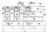
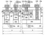
도 1a 내지 도 1h는 본 발명의 일 실시예에 따른 반도체소자를 나타낸 평면도들이고, 도 2a 내지 도 2c, 도 3a 내지 도 3c, 도 4a 내지 도 4c, 도 5a 내지 도 5c, 도 6a 내지 도 6c, 도 7a 내지 도 7c, 도 8a 내지 도 8c, 도 9a 내지 도 9c, 및 도 10a 내지 도 10c는 본 발명의 일 실시예에 따른 반도체소자를 나타낸 단면도들이다. 도 11a 내지 도 11e는 본 발명의 다른 실시예에 따른 반도체소자를 나타낸 평면도들이고, 도 12a 내지 도 12e는 본 발명의 다른 실시예에 따른 반도체소자를 나타낸 단면도들이고, 도 13은 본 발명의 또 다른 실시예에 따른 반도체소자를 나타낸 평면도이고, 도 14는 본 발명의 일 실시예에 따른 반도체소자의 제조방법을 나타낸 개략적인 공정 흐름도이고, 도 15는 본 발명의 다른 실시예에 따른 반도체소자의 제조방법을 나타낸 개략적인 공정 흐름도이고, 도 16은 본 발명의 실시예들에 의해 제조된 반도체소자를 나타낸 평면도이고, 도 17은 본 발명의 또 다른 실시예들에 의해 제조된 반도체소자를 나타낸 단면도이다.1A to 1H are plan views illustrating a semiconductor device according to an embodiment of the present invention, and FIGS. 2A to 2C, 3A to 3C, 4A to 4C, 5A to 5C, and 6A to 6C. 7A to 7C, 8A to 8C, 9A to 9C, and 10A to 10C are cross-sectional views illustrating semiconductor devices according to example embodiments. 11A to 11E are plan views illustrating semiconductor devices according to other embodiments of the inventive concept, FIGS. 12A to 12E are cross-sectional views illustrating semiconductor devices according to other embodiments of the present invention, and FIG. 13 is still another embodiment of the present invention. 14 is a plan view illustrating a semiconductor device in accordance with an embodiment, and FIG. 14 is a schematic process flowchart illustrating a method of manufacturing a semiconductor device in accordance with an embodiment of the present invention. FIG. 15 is a semiconductor device manufacturing in accordance with another embodiment of the present invention. A schematic process flow diagram illustrating a method, FIG. 16 is a plan view showing a semiconductor device manufactured by embodiments of the present invention, and FIG. 17 is a cross-sectional view showing a semiconductor device manufactured by another embodiment of the present invention. .
도 1a 내지 도 1h, 도 2a 내지 도 2c, 도 3a 내지 도 3c, 도 4a 내지 도 4c, 도 5a 내지 도 5c, 도 6a 내지 도 6c, 도 7a 내지 도 7c, 도 8a 내지 도 8c, 도 9a 내지 도 9c, 및 도 10a 내지 도 10c에 있어서, 참조부호 "A"는 제1 소자 영역을 나타내고, 참조부호 "B"는 제2 소자 영역을 나타내고, 참조부호 "C"는 제3 소자 영역을 나타낸다. 도 2a, 도 3a, 도 4a, 도 5a, 도 6a, 도 7a, 도 8a, 도 9a 및 도 10a 에 있어서, 참조부호 "D"는 도 1a 내지 도 1h에서의 I-I′선을 따라 취해진 영역을 나타내고, 참조부호 "E"는 도 1a 내지 도 1h에서의 II-II′선을 따라 취해진 영역을 나타낸다. 도 2b, 도 3b, 도 4b, 도 5b, 도 6b, 도 7b, 도 8b, 도 9b 및 도 10b에 있어서, 참조부호 "F"는 도 1a 내지 도 1h에서의 III-III′선을 따라 취해진 영역을 나타내고, 참조부호 "G"는 도 1a 내지 도 1h에서의 IV-IV′선을 따라 취해진 영역을 나타낸다. 도 2c, 도 3c, 도 4c, 도 5c, 도 6c, 도 7c, 도 8c, 도 9c 및 도 10c에 있어서, 참조부호 "H"는 도 1a 내지 도 1h에서의 V-V′선을 따라 취해진 영역을 나타내고, 참조부호 "I"는 도 1a 내지 도 1h에서의 VI-VI′선을 따라 취해진 영역을 나타낸다.1A to 1H, 2A to 2C, 3A to 3C, 4A to 4C, 5A to 5C, 6A to 6C, 7A to 7C, 8A to 8C, and 9A. 9C and 10A to 10C, reference numeral "A" denotes a first element region, reference numeral "B" denotes a second element region, and reference numeral "C" denotes a third element region. Indicates. 2A, 3A, 4A, 5A, 6A, 7A, 8A, 9A and 10A, reference numeral “D” denotes an area taken along the line II ′ in FIGS. 1A to 1H. And reference numeral “E” denotes a region taken along the line II-II 'in FIGS. 1A to 1H. 2B, 3B, 4B, 5B, 6B, 7B, 8B, 9B and 10B, reference numeral “F” is taken along the line III-III ′ in FIGS. 1A-1H. Areas are shown, and reference numeral “G” denotes an area taken along the line IV-IV ′ in FIGS. 1A to 1H. 2C, 3C, 4C, 5C, 6C, 7C, 8C, 9C and 10C, reference numeral “H” denotes an area taken along the line VV ′ in FIGS. 1A to 1H. And reference numeral "I" represents a region taken along the line VI-VI 'in FIGS. 1A to 1H.
도 11a 내지 도 11e, 및 도 12a 내지 도 12e에 있어서, 참조부호 "J"는 플로팅 바디 소자 영역을 나타내고, 참조부호 "K"는 벌크 소자 영역을 나타낸다. 도 12a 내지 도 12e에 있어서, 참조부호 "L"은 도 11a 내지 도 11e의 VII-VII′선을 따라 취재진 영역을 나타내고, 참조부호 "M"은 도 11a 내지 도 11e의 VIII-VIII′선을 따라 취해진 영역을 나타낸다. 그리고, 도 12a 내지 도 12e에 있어서, 참조부호 "K"는 도 11a 내지 도 11e의 VIIII-VIIII′선을 따라 취해진 벌크 소자 영역을 나타낸다.11A to 11E and 12A to 12E, reference numeral "J" denotes a floating body element region, and reference numeral "K" denotes a bulk element region. In Figs. 12A to 12E, reference numeral "L" denotes an area covered along line VII-VII 'of Figs. 11A to 11E, and reference numeral "M" denotes VIII-VIII' line of Figs. 11A to 11E. Indicate the area taken along. 12A to 12E, reference numeral K denotes a bulk element region taken along the line VIIII-VIIII 'of FIGS. 11A to 11E.
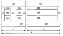
우선, 도 1h, 도 10a, 도 10b 및 도 10c를 참조하여 본 발명의 일 실시예에 따른 반도체소자의 구조에 대해 설명하기로 한다.First, a structure of a semiconductor device according to an exemplary embodiment of the present invention will be described with reference to FIGS. 1H, 10A, 10B, and 10C.
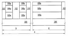
도 1h, 도 10a, 도 10b 및 도 10c를 참조하면, 복수개의 소자영역들을 갖는 기판(100)이 제공될 수 있다. 상기 기판(100)은 실리콘 기판일 수 있다. 상기 기판(100)은 벌크 바디 소자영역과 플로팅 바디 소자영역들을 가질 수 있다. 상기 기판(100)은 상기 플로팅 바디 소자영역들 중의 제1 소자 영역(A), 상기 플로팅 바디 소자 영역들 중의 제2 소자 영역(B) 및 상기 플로팅 바디 소자 영역들 중의 제3 소자 영역(C)을 가질 수 있다. 상기 제1 소자 영역(A)은 제1 메모리 셀 어레이 영역이고, 상기 제2 소자 영역(B)은 제2 메모리 셀 어레이 영역이고, 상기 제3 소자 영역(C)은 제3 메모리 셀 어레이 영역일 수 있다. 그러나, 이에 한정되지 않는다. 예를 들어, 상기 제1 내지 제3 소자 영역들(A, B, C) 중 일부는 전계효과 트랜지스터 영역들로 구성된 집적 회로 영역들일 수 있다.1H, 10A, 10B, and 10C, a
상기 제1 소자 영역(A)의 상기 기판 상에 차례로 적층된 제1 매립 패턴들(124a) 및 제1 활성 패턴들(106a), 상기 제2 소자 영역(B)의 상기 기판 상에 차례로 적층된 제2 매립 패턴들(124b) 및 제2 활성 패턴들(106b), 상기 제3 소자 영역(C)의 상기 기판 상에 차례로 적층된 제3 매립 패턴들(124c) 및 제3 활성 패턴들(106c), 및 상기 벌크 바디 소자영역의 활성영역을 한정하는 소자분리막(112)이 제공될 수 있다. 상기 소자분리막(112)은 실리콘 산화막과 같은 절연막으로 이루어질 수 있다.First buried
상기 제1 매립 패턴들(124a)은 n형 도우프트 반도체 물질막, p형 도우프트 반도체 물질막, 언도우프트(undoped) 반도체물질막 또는 금속 물질막으로 이루어질 수 있다. 상기 반도체물질막은 실리콘막일 수 있고, 상기 금속 물질막은 타이타늄 질화막(TiN layer) 또는 탄탈륨 질화막(TaN layer)일 수 있다. 상기 제2 매립 패턴들(124b)은 n형 도우프트 실리콘막, p형 도우프트 실리콘막, 언도우프트(undoped) 실리콘막 또는 금속 물질막으로 이루어질 수 있다. 상기 제3 매립 패턴들(124c)은 n형 도우프트 실리콘막, p형 도우프트 실리콘막, 언도우프트(undoped) 실리콘막 또는 금속 물질막으로 이루어질 수 있다.The first buried
상기 제1 내지 제3 매립 패턴들(124a, 124b, 124c)은 같은 두께를 가질 수 있다. 이와는 달리, 상기 제1 내지 제3 매립 패턴들(124a, 124b, 124c) 중 적어도 하나의 패턴은 다른 두께를 가질 수 있다.The first to third
상기 제1 내지 제3 매립 패턴들(124a, 124b, 124c)은 같은 물질로 이루어질 수 있다. 이와는 달리, 상기 제1 내지 제3 매립 패턴들(124a, 124b, 124c) 중 적어도 하나는 나머지와 다른 특성의 물질로 이루어질 수 있다.The first to third
상기 제1 내지 제3 활성 패턴들(106a, 106b, 106c)은 반도체 물질막으로 이루어질 수 있다. 예를 들어, 상기 제1 내지 제3 활성 패턴들(106a, 106b, 106c)은 단결정 실리콘막으로 이루어질 수 있다. 상기 제1 내지 제3 활성 패턴들(106a, 106b, 106c)은 같은 두께를 가질 수 있다. 이와는 달리, 상기 제1 내지 제3 활성 패턴들(106a, 106b, 106c)은 서로 다른 두께들을 가질 수 있다.The first to third
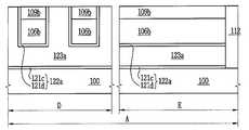
상기 제1 소자영역(A)에서, 상기 제1 활성 패턴들(106a)은 상기 제1 매립 패턴들(124a) 상에 자기정렬될 수 있다. 그리고, 상기 제1 매립 패턴들(124a)은 서로 이격되어 전기적으로 분리될 수 있다. 상기 제1 매립 패턴들(124a)은 상기 제1 소 자 영역(A)에 제공되는 트랜지스터와 같은 소자의 백 게이트 전극일 수 있다. 따라서, 상기 제1 매립 패턴들(124a)의 각각에 독립적인 전기적 신호를 인가할 수 있다. 한편, 상기 제1 매립 패턴들(124a)이 언도우프트 실리콘막으로 이루어진 경우에, 상기 제1 매립 패턴들(124a)은 유전체와 같은 역할을 할 수 있다.In the first device region A, the first
상기 제1 매립 유전막(122a)은 상기 제1 매립 패턴들(124a)과 상기 기판(100) 사이에 개재된 제1 하부 매립 유전막(121a)이 제공될 수 있다. 상기 제1 활성 패턴들(106a)과 상기 제1 매립 패턴들(124a) 사이에 개재된 제1 상부 매립 유전막(121b)이 제공될 수 있다. 여기서, 상기 제1 하부 매립 유전막(121) 및 상기 제1 상부 매립 유전막(121b)은 제1 매립 유전막(122a)을 구성할 수 있다. 상기 제1 매립 유전막(122a)은 실리콘 산화막 또는 실리콘 산화막보다 높은 유전상수를 갖는 고유전막(high-k dielectric layer)으로 이루어질 수 있다.The first buried
다른 실시예에서, 상기 제1 매립 유전막(122a)은 정보 저장 물질막을 포함할 수 있다. 상기 정보 저장 물질막은 플래쉬 메모리 소자의 전하 저장층(charge trap layer)일 수 있다. 예를 들어, 상기 제1 매립 유전막(122a)은 제1 산화막, 전하 저장층으로서의 질화막 및 제2 산화막으로 이루어진 ONO막일 수 있다. 한편, 상기 정보 저장 물질막으로서 나노 크리스탈(nano crystal) 물질을 이용할 수도 있다.In another embodiment, the first buried
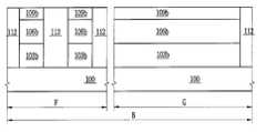
상기 제2 소자영역(B)에서, 상기 제2 매립 패턴들(124b)을 전기적으로 접속시키는 적어도 하나의 제1 연결부(125b)가 제공될 수 있다. 따라서, 상기 제2 매립 패턴들(124b)은 상기 제1 연결부(125b)에 의해 전기적으로 접속되어 상기 제2 소자 영역(B)에 제공되는 소자의 공통 백 게이트 전극으로 이용될 수 있다. 상기 제1 연 결부(125b)는 상기 제2 매립 패턴들(124b)로부터 연장되어 상기 제2 매립 패턴들(124b)과 동일한 물질로 이루어질 수 있다. 그리고, 상기 제1 연결부(125b)는 상기 제2 매립 패턴들(124b)과 실질적으로 동일한 레벨에 위치할 수 있다. 한편, 상기 제2 매립 패턴들(124b)이 언도우프트 실리콘막으로 이루어진 경우에, 상기 제2 매립 패턴들(124b)은 유전체와 같은 역할을 할 수 있다.In the second device region B, at least one
상기 제2 매립 패턴들(124b)과 상기 기판(100) 사이에 개재됨과 아울러 상기 제1 연결부(125b)와 상기 기판(200) 사이에 개재된 제2 하부 매립 유전막(121c)이 제공될 수 있다. 상기 제2 활성 패턴들(106b)과 상기 제2 매립 패턴들(124b) 사이에 개재된 제2 상부 매립 유전막(121d)이 제공될 수 있다. 상기 제2 하부 매립 유전막(121c) 및 상기 제2 상부 매립 유전막(121d)은 제2 매립 유전막(122b)을 구성할 수 있다. 상기 제2 매립 유전막(122b)은 실리콘 산화막 또는 실리콘 산화막보다 높은 유전상수를 갖는 고유전막(high-k dielectric layer)으로 이루어질 수 있다.A second lower buried
다른 실시예에서, 상기 제2 매립 유전막(122b)은 정보 저장 물질막을 포함할 수 있다. 상기 정보 저장 물질막은 플래쉬 메모리 소자의 전하 저장층(charge trap layer)일 수 있다.In another embodiment, the second buried
상기 제3 소자영역(C)에서, 상기 제3 매립 패턴들(124c)을 전기적으로 접속시키는 적어도 하나의 제2 연결부(125c)가 제공될 수 있다. 상기 제2 연결부(125c)는 상기 제3 매립 패턴들(124c)로부터 연장되어 상기 제3 매립 패턴들(124c)과 동일한 물질로 이루어질 수 있다. 그리고, 상기 제2 연결부(125c)는 상기 제3 활성 패턴들(106c)의 측벽들을 덮을 수 있다. 따라서, 상기 제3 매립 패턴들(124c)은 상 기 제2 연결부(125c)에 의해 전기적으로 접속되어 상기 제3 소자 영역(C)에 제공되는 소자의 공통 백 게이트 전극으로 이용될 수 있다. 이때, 상기 제3 활성 패턴들(106c)의 바닥면들 및 측벽들이 상기 제3 매립 패턴들(124c) 및 상기 제3 연결부(125c)에 의해 덮이므로, 상기 제3 소자 영역(C)에 형성되는 트랜지스터의 문턱전압은 상기 제3 소자 영역(C)의 상기 공통 백 게이트 전극에 의해 용이하게 제어할 수 있다. 한편, 상기 제3 매립 패턴들(124c)이 언도우프트 실리콘막으로 이루어진 경우에, 상기 제3 매립 패턴들(124c)은 유전체와 같은 역할을 할 수 있다.In the third device region C, at least one
상기 제3 매립 패턴들(124c)과 상기 기판(100) 사이에 개재됨과 아울러 상기 제2 연결부(125c)와 상기 기판(100) 사이에 개재된 제3 하부 매립 유전막(121e)이 제공될 수 있다. 상기 제3 활성 패턴들(106c)과 상기 제3 매립 패턴들(124c) 사이에 개재됨과 아울러 상기 제3 활성 패턴들(106c)과 상기 제2 연결부(125c) 사이에 개재된 제3 상부 매립 유전막(121f)이 제공될 수 있다. 상기 제3 하부 및 상부 매립 유전막들(121e, 121f)은 제3 매립 유전막(122c)을 구성할 수 있다. 상기 제3 매립 유전막(122c)은 실리콘 산화막 또는 고유전막(high-k dielectric layer)으로 이루어질 수 있다.A third lower buried
다른 실시예에서, 상기 제3 매립 유전막(122c)은 정보 저장 물질막을 포함할 수 있다. 상기 정보 저장 물질막은 플래쉬 메모리 소자의 전하 저장층(charge trap layer)일 수 있다. .In another embodiment, the third buried
상기 제1 소자 영역(A)에서, 상기 제1 매립 패턴들(124a)은 전기적으로 분리될 수 있다. 따라서, 상기 제1 매립 패턴들(124a)의 각각에 독립적인 전기적 신호 를 인가할 수 있다. 이와는 달리, 상기 제2 소자 영역(B)에서의 상기 제2 매립 패턴들(124b)은 상기 제1 연결부(125b)에 의해 서로 전기적으로 접속될 수 있다. 이와 마찬가지로, 상기 제3 소자 영역(C)의 상기 제3 매립 패턴들(124c)은 서로 전기적으로 연결될 수 있다.In the first device region A, the first buried
상술한 바와 같은 상기 제1 내지 제3 소자 영역들(A, B, C)에서의 상기 제1 내지 제3 매립 패턴들(124a, 124b, 124c), 상기 제1 내지 제3 활성 패턴들(106a, 106b, 106c) 및 상기 제1 내지 제3 매립 유전막들(122a, 122b, 122c)을 갖는 기판 상에 다양한 기능을 수행하는 소자들을 형성할 수 있다. 즉, 상술한 상기 제1 내지 제3 소자 영역들(A, B, C)에 다양한 구조의 소자들을 제공할 수 있다. 또한, 벌크 소자 영역에 형성하는 소자와 조합하여 하나의 반도체 칩 내에 다양한 소자들을 구성할 수 있다.The first to third
이하에서, 제1 소자 영역(A)에 비휘발성 메모리 셀 어레이 영역을 구성하는 게이트 구조 및 배선 구조를 설명하고, 상기 제2 소자 영역(B)에 제1 휘발성 메모리 셀 어레이 영역을 구성하는 게이트 구조 및 배선 구조를 설명하고, 상기 제3 소자 영역(C)에 제2 휘발성 메모리 셀 어레이 영역을 구성하는 게이트 구조 및 배선 구조를 설명하기로 한다.Hereinafter, a gate structure and a wiring structure constituting the nonvolatile memory cell array region in the first device region A will be described, and a gate structure constituting the first volatile memory cell array region in the second device region B will be described. And a wiring structure, and a gate structure and a wiring structure constituting the second volatile memory cell array region in the third device region C will be described.
상기 제1 소자 영역(A)에서, 상기 제1 활성 패턴들(106a) 상에 제1 게이트 구조체들(136a)이 제공될 수 있다. 상기 게이트 구조체들(136a)은 상기 각 제1 활성 패턴들(106a) 상에 복수개가 제공될 수 있다. 따라서, 상기 게이트 구조체 들(136a)은 상기 제1 활성 패턴들(106a) 상에서 서로 이격된 아일랜드 형(island-type)으로 제공될 수 있다. 상기 제1 게이트 구조체들(136a)의 각각은 차례로 적층된 제1 게이트 유전막(130a) 및 제1 게이트 전극(133a)을 포함할 수 있다. 상기 제1 게이트 유전막(130a)은 정보 저장 물질막을 포함할 수 있다. 상기 정보 저장 물질막은 플래쉬 메모리 소자의 전하 저장층(charge trap layer)일 수 있다.In the first device region A,
한편, 상기 제1 게이트 유전막(130a)은 상기 제1 매립 유전막(122a)과 동일한 물질로 이루어질 수 있다. 예를 들어, 상기 제1 매립 유전막(122a)이 정보 저장 물질막을 포함하고, 상기 제1 게이트 유전막(130a)이 상기 제1 매립 유전막(122a)과 동일한 물질로 이루어진 경우에, 상기 제1 소자 영역(A)은 멀티 비트 저장 노드를 갖는 플래쉬 메모리 소자의 셀 영역으로 이용될 수 있다. 더 나아가, 상기 제1 게이트 유전막(130a)과 상기 제1 매립 유전막(122a)이 서로 동일한 물질로 이루어짐과 아울러 서로 같은 두께인 경우에, 동일한 동작 전압에 의해 플래쉬 메모리 셀의 프로그래밍/소거/읽기 동작이 이루어질 수 있다.The first
한편, 상기 제1 게이트 구조체(136a)는 차례로 적층된 게이트 유전막, 플로팅 게이트, 게이트간 유전막 및 제어 게이트 전극으로 이루어진 플래쉬 메모리 소자의 셀 게이트 구조체일 수 있다.The
상기 제2 소자 영역(B)에서, 상기 제2 활성 패턴들(106b) 상에 적어도 하나의 제2 게이트 구조체(136b)가 제공될 수 있다. 상기 제2 게이트 구조체들(136b)은 상기 제2 활성 패턴들(106b)의 측벽들을 덮을 수 있다. 상기 제2 게이트 구조체(136b)는 차례로 적층된 제2 게이트 유전막(130b) 및 제2 게이트 전극(133b)을 포함할 수 있다. 상기 제2 게이트 전극(133b)은 상기 제2 활성 패턴들(106b)과 교차하는 방향성을 갖는 라인 형상일 수 있다. 상기 제2 게이트 유전막(130b)은 실리콘 산화막 또는 상기 실리콘 산화막보다 높은 유전상수를 갖는 고유전막으로 이루어질 수 있다. 상기 제2 게이트 전극(133b)은 도전성 물질막으로 이루어질 수 있다.In the second device region B, at least one
상기 제3 소자 영역(C)에서, 상기 제3 활성 패턴들(106c) 상에 적어도 하나의 제3 게이트 구조체(136c)가 제공될 수 있다. 상기 제3 게이트 구조체(136c)는 차례로 적층된 제3 게이트 유전막(130c) 및 제3 게이트 전극(133c)을 포함할 수 있다. 상기 제3 게이트 전극(133c)은 상기 제3 활성 패턴들(106c)과 교차하는 방향성을 갖는 라인 형상일 수 있다. 상기 제3 게이트 전극(133c)은 메모리 소자의 워드라인으로 정의할 수 있다. 상기 제3 게이트 유전막(130c)은 실리콘 산화막 또는 상기 실리콘 산화막보다 높은 유전상수를 갖는 고유전막으로 이루어질 수 있다. 상기 제3 게이트 전극(133c)은 도전성 물질막으로 이루어질 수 있다.In the third device region C, at least one
상기 제1 게이트 구조체들(136a) 양 옆의 상기 제1 활성 패턴들(106a)에 제1 소스/드레인 영역들(145a)이 제공될 수 있다. 상기 제2 게이트 구조체들(136b) 양 옆의 상기 제2 활성 패턴들(106b)에 제2 소스/드레인 영역들(145b)이 제공될 수 있다. 상기 제3 게이트 구조체들(136c) 양 옆의 상기 제3 활성 패턴들(106c)에 제3 소스/드레인 영역들(145c)이 제공될 수 있다. 상기 제1 내지 제3 게이트 구조체들(136a, 136b, 136c)을 갖는 기판 상에 차례로 적층된 하부 층간절연막(147) 및 상부 층간절연막(151)이 제공될 수 있다.First source /
상기 제1 소자 영역(A)에서, 상기 하부 층간절연막(147)을 관통하며 상기 제1 활성 패턴들(106a)을 가로지르고 상기 제1 소스/드레인 영역들(145a)과 전기적으로 접속된 제1 하부 도전성 패턴들(148)이 제공될 수 있다. 상기 제1 하부 도전성 패턴들(148)은 메모리 소자의 비트라인으로 정의할 수 있다. 상기 제1 게이트 구조체들(136a)은 상기 제1 활성 패턴들(106a) 상에서 아일랜드형으로 복수개가 제공될 수 있다. 따라서, 상기 제1 게이트 구조체들(136a)의 각각은 상기 제1 하부 도전성 패턴들(148) 사이에 위치할 수 있다.In the first device region A, a first penetrating through the lower
상기 상부 층간절연막(147) 상에 제1 상부 도전성 패턴들(157a)이 제공될 수 있다. 상기 제1 상부 도전성 패턴들(157a)의 각각은 상기 제1 하부 도전성 패턴들(148)과 교차하는 방향성을 갖는 라인 형상이며, 상기 제1 게이트 구조체들(136a)과 중첩할 수 있다. 상기 제1 상부 도전성 패턴들(157a)은 메모리 소자의 워드라인으로 정의할 수 있다. 상기 제1 상부 도전성 패턴들(157a)과 상기 제1 게이트 구조체들(136a) 사이에 제1 게이트 콘택 구조체들(154a)이 제공될 수 있다.First upper
상기 상부 층간절연막(151) 및 상기 하부 층간절연막(147)을 차례로 관통하며 각각의 상기 제1 매립 패턴들(124b)에 전기적으로 접속된 제1 하부 게이트 콘택 구조체들(155b)이 제공될 수 있다. 상기 상부 층간절연막(151) 상에 상기 제1 하부 게이트 콘택 구조체들(155b)을 각각 덮는 제1 하부 게이트 배선들(157b)이 제공될 수 있다. 따라서, 상기 제1 소자 영역(A)에서, 상기 제1 매립 패턴들(124a) 및 상기 제1 활성 패턴들(106a)을 갖는 기판 상에 상술한 바와 같은 비휘발성 메모리 소자의 배선 구조가 제공될 수 있다.First lower
상기 제2 소자 영역(B)에서, 상기 하부 층간절연막(147)을 관통하며 상기 제2 소스/드레인 영역들(145b) 중 하나에 전기적으로 접속하고, 상기 제2 활성 패턴들(106b)을 가로지르는 라인 형상의 제2 하부 도전성 패턴들(149a)이 제공될 수 있다. 그리고, 상기 하부 층간절연막(147)을 관통하며 상기 제2 소스/드레인 영역들(145b) 중 다른 하나에 전기적으로 접속하는 아일랜드형의 제2 하부 콘택 구조체들(149b)이 제공될 수 있다. 상기 제2 하부 도전성 패턴들(149a) 및 상기 제2 하부 콘택 구조체들(149b)은 동일한 물질로 이루어질 수 있다.In the second device region B, the lower
상기 상부 층간절연막(151)을 관통하며 상기 제2 하부 콘택 구조체들(149b)과 전기적으로 접속하는 제2 상부 콘택 구조체들(154b)이 제공될 수 있다. 상기 상부 층간절연막(151) 상에 상기 제2 상부 콘택 구조체들(154b)을 덮으며 상기 제2 게이트 전극들(133b)과 교차하는 방향성을 갖는 라인 형상의 제2 상부 도전성 패턴들(158a)이 제공될 수 있다.Second
상기 상부 층간절연막(151) 및 상기 하부 층간절연막(147)을 차례로 관통하며 상기 제2 매립 패턴들(124b)과 전기적으로 접속하는 제2 하부 게이트 콘택 구조체(155b)가 제공될 수 있다. 상기 상부 층간절연막(151) 상에 상기 제2 하부 게이트 콘택 구조체(155b)를 덮는 제2 하부 게이트 배선(158b)이 제공될 수 있다.A second lower
상기 제3 소자 영역에서, 상기 하부 층간절연막(147)을 관통하며 상기 제3 소스/드레인 영역들(145c) 중 하나에 전기적으로 접속하고, 상기 제3 활성 패턴들(106c)을 가로지르는 라인 형상의 제3 하부 도전성 패턴들(150a)이 제공될 수 있다. 그리고, 상기 하부 층간절연막(147)을 관통하며 상기 제3 소스/드레인 영역 들(145c) 중 다른 하나에 전기적으로 접속하는 아일랜드형의 제3 하부 콘택 구조체들(150b)이 제공될 수 있다. 상기 제3 하부 도전성 패턴들(150a) 및 상기 제3 하부 콘택 구조체들(150b)은 동일한 물질로 이루어질 수 있다. 상기 제3 하부 도전성 패턴들(150a)은 공통 소스 라인(CSL)으로 정의할 수 있다.In the third device region, a line shape penetrates the lower
상기 상부 층간절연막(151)을 관통하며 상기 제3 하부 콘택 구조체들(150b)과 전기적으로 접속하는 제3 상부 콘택 구조체들(154c)이 제공될 수 있다. 상기 상부 층간절연막(151) 상에 상기 제3 상부 콘택 구조체들(154c)을 덮으며 상기 제3 게이트 전극들(133c)과 교차하는 방향성을 갖는 라인 형상의 제3 상부 도전성 패턴들(159a)이 제공될 수 있다. 상기 제3 상부 도전성 패턴들(109a)은 메모리 소자의 비트라인으로 정의할 수 있다.Third
한편, 상기 제3 소스/드레인 영역들(145c) 사이에 위치하며, 상기 제3 게이트 구조체(136c) 하부에 위치하는 상기 제3 활성 패턴들(106c)은 메모리 소자의 정보 저장 영역으로 정의될 수 있다. 따라서, 플로팅 바디 디램(DRAM)과 같은 메모리 소자가 제공될 수 있다. 또한, 상기 제3 활성 패턴들(106c)은 측벽들 및 바닥면들이 상기 제3 매립 패턴들(124c) 및 상기 제3 연결부들(125c)에 의해 덮일 수 있다. 따라서, 상기 제3 연결부들(125c)은 상기 제3 매립 패턴들(124c)을 서로 전기적으로 접속시키므로, 백 게이트 전극으로 작용하는 상기 제3 매립 패턴들(124c)에 의해 상기 제3 소자 영역(C)에 형성되는 소자의 문턱전압을 용이하게 제어할 수 있다. 상기 상부 층간절연막(151) 및 상기 하부 층간절연막(147)을 차례로 관통하며 상기 제3 매립 패턴들(124c)과 전기적으로 접속하는 제3 하부 게이트 콘택 구조 체(155c)가 제공될 수 있다. 상기 상부 층간절연막(151) 상에 상기 제3 하부 게이트 콘택 구조체(155c)를 덮는 제3 하부 게이트 배선(159b)이 제공될 수 있다.Meanwhile, the third
상술한 바와 같이, 상기 제1 활성 패턴들(106a) 상에 비휘발성 메모리 소자의 셀 게이트 및 배선 구조가 제공되고, 상기 제2 및 제3 활성 패턴들(106b, 106c) 상에 휘발성 메모리 소자의 셀 게이트 및 배선 구조가 제공될 수 있다. 그러나, 이에 한정되지 않는다. 예를 들어, 상기 제1 소자 영역(A)에서, 상기 제1 활성 패턴들(106a) 상에 상기 제 2 및 제3 소자 영역들(B, C)에서의 셀 게이트 및 배선 구조가 제공될 수도 있다. 이와 마찬가지로, 상기 제2 및 제3 활성 패턴들(106b, 106c) 상에 상기 제1 소자 영역(A)에서의 셀 게이트 및 배선 구조가 제공될 수 있다. 여기서, 상기 제1 소자 영역(A)에서의 셀 게이트 및 배선 구조는 상기 제1 게이트 구조체(136a), 상기 제1 하부 도전성 패턴들(148) 및 상기 제1 상부 도전성 패턴들(157a)을 포함할 수 있다. 상기 제2 소자 영역(B)에서의 셀 게이트 및 배선 구조는 상기 제2 게이트 구조체(136b), 상기 제2 하부 도전성 패턴들(149a), 상기 제2 하부 콘택 구조체(149b) 및 상기 제2 상부 도전성 패턴들(158a)을 포함할 수 있다. 상기 제3 소자 영역(C)에서의 셀 게이트 및 배선 구조는 상기 제3 게이트 구조체(136c), 상기 제3 하부 도전성 패턴들(150a), 상기 제3 하부 콘택 구조체(150b) 및 상기 제3 상부 도전성 패턴들(159a)을 포함할 수 있다.As described above, a cell gate and a wiring structure of a nonvolatile memory device are provided on the first
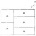
따라서, 상술한 바와 같은 다양한 구조의 소자들을 갖는 시스템 온 칩(system on chip)과 같은 반도체소자을 제공할 수 있다. 예를 들어, 도 16에 도시된 바와 같이, 제1 영역(500), 제2 영역(510), 제3 영역(520), 제4 영역(530) 및 제5 영역(540)을 갖는 반도체소자(550)가 제공될 수 있다. 상기 제1 내지 제3 영역들(500, 510, 520)은 상기 제2 매립 패턴들(124b) 및 상기 제2 매립 패턴들(124b)을 연결하는 상기 제2 연결부들(125b)을 갖는 소자 영역일 수 있다. 전기적으로 서로 연결된 상기 제2 매립 패턴들(124b), 즉 제2 백 게이트 전극을 갖는 기판 상에 형성된 반도체소자가 상기 제1 내지 제3 영역들(500, 510, 520)에 제공될 수 있다. 예를 들어, 상기 제1 영역(500)에 고성능(high performance) 트랜지스터들이 제공될 수 있고, 상기 제2 영역(510)에 에스램(SRAM)과 같은 캐쉬 메모리가 제공될 수 있다. 그리고, 상기 제3 영역(520)에 저전력 트랜지스터들이 제공될 수 있다. 상기 제4 영역(530)에 상기 제3 매립 패턴들(124c) 및 상기 제3 매립 패턴들(124c)을 전기적으로 연결하며 상기 제3 활성 패턴들(106c)의 측벽들을 덮는 제3 연결부들(125c)을 갖는 기판 상에 형성된 반도체소자가 제공될 수 있다. 예를 들어, 상기 제4 영역(530)에 플로팅 바디 디램과 같은 메모리 소자가 제공될 수 있다. 상기 제5 영역(540)에 상기 제1 매립 패턴들(124a)과 같은 백 게이트 전극을 갖는 기판 상에 형성된 소자가 제공될 수 있다. 예를 들어, 상기 제5 영역(540)에 멀티 비트 저장 노드를 갖는 플래쉬 메모리 소자가 제공될 수 있다.Accordingly, it is possible to provide a semiconductor device such as a system on chip having elements of various structures as described above. For example, as illustrated in FIG. 16, a semiconductor device having a
이와 같은 반도체소자(550) 상에 다양한 집적회로 장치를 갖는 반도체소자가 제공될 수 있다. 예를 들어, 도 17에 도시된 바와 같이, 수직적으로 집적된 반도체소자가 제공될 수 있다. 도 17을 참조하면, 상술한 반도체소자(550) 상에 제1 패시베이션막(560)이 제공될 수 있다. 상기 제1 패시베이션막(560)은 절연막일 수 있다. 상기 제1 패시베이션막(560) 상에 반도체 집적 회로를 구비하는 다른 반도체소 자, 즉 집적회로기판(600)이 제공될 수 있다. 상기 집적회로기판(600)은 전체 반도체소자의 평면크기를 감소시키기 위하여 제공될 수 있다. 예를 들어, 상기 집적회로기판(600)에는 상기 반도체소자(550)의 기판과 동종 및/또는 이종의 집적 회로가 제공될 수 있다. 상기 집적회로기판(600)과 상기 반도체소자(550)를 전기적으로 연결하는 기판간 배선(610)이 제공될 수 있다. 상기 다른 반도체소자(600) 및 상기 기판간 배선(610)을 덮는 제2 패시베이션막(620)이 제공될 수 있다. 상기 제2 패시베이션막(620) 상에 하나 또는 복수개의 적층된 또 다른 집적회로기판이 제공될 수도 있다. 이와 같이, 본 발명의 실시예들에 따른 반도체소자(550)와 집적회로기판(600)을 수직적으로 배치함으로 인하여 다양한 기능을 갖는 반도체소자를 제공할 수 있다.A semiconductor device having various integrated circuit devices may be provided on the
다음으로, 도 11e 및 도 12e를 참조하여 본 발명의 다른 실시예들에 따른 반도체소자의 구조를 설명하기로 한다.Next, a structure of a semiconductor device according to other exemplary embodiments of the present invention will be described with reference to FIGS. 11E and 12E.
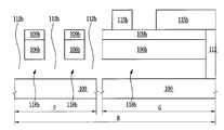
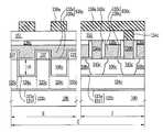
도 11e 및 도 12e를 참조하면, 복수개의 소자 영역들을 갖는 기판(200)이 제공될 수 있다. 예를 들어, 상기 기판(200)은 플로팅 바디 소자영역(J)과 벌크 바디 소자영역(K)을 가질 수 있다. 상기 기판(200)은 반도체 기판일 수 있다. 예를 들어, 상기 기판(200)은 실리콘 기판일 수 있다.11E and 12E, a
상기 플로팅 바디 소자영역(J)에서, 상기 기판(200) 상에 활성 패턴들(224)이 제공될 수 있다. 그리고, 상기 활성 패턴들(224) 사이를 연결하는 연결부들(224a)이 제공될 수 있다. 도 11e에 도시된 바와 같이 상기 연결부들(224a)은 서 로 이격될 수 있다. 상기 각 매립 패턴들(224) 상에 복수개의 상기 활성 패턴들(206b)이 제공될 수 있다. 즉, 하나의 상기 매립 패턴(224) 상에 복수개의 상기 활성 패턴들(206b)이 제공될 수 있다. 상기 매립 패턴들(224)과 상기 기판(200) 사이 및 상기 연결부들(224a)과 상기 기판(200) 사이에 개재된 하부 매립 유전막(221b)이 제공될 수 있다. 상기 매립 패턴들(224)과 상기 활성 패턴들(206b) 사이에 상부 매립 유전막(221a)이 제공될 수 있다. 상기 상부 및 하부 매립 유전막들(221a, 221b)은 매립 유전막(222a)을 구성할 수 있다.In the floating body device region J,
상기 플로팅 바디 소자영역(J)의 상기 매립 패턴들(224) 및 상기 활성 패턴들(206b)을 한정함과 아울러 상기 벌크 바디 소자영역(K)의 활성영역(212a)을 한정하는 제1 및 제2 소자분리막들(212, 227)이 제공될 수 있다. 좀더 구체적으로, 상기 제1 소자분리막(212)은 상기 플로팅 바디 소자영역(J)의 상기 매립 패턴들(224)을 한정함과 아울러 상기 벌크 바디 소자 영역(K)의 상기 활성영역(212a)을 한정하고, 상기 제2 소자분리막(227)은 상기 매립 패턴들(224) 상의 상기 활성 패턴들(206b)을 한정할 수 있다.First and second defining the buried
상기 활성 패턴들(206b)을 가로지르는 적어도 하나의 제1 게이트 구조체(236a)가 제공될 수 있다. 상기 제1 게이트 구조체(236a)는 차례로 적층된 제1 게이트 유전막(230a) 및 제1 게이트 전극(233a)을 포함할 수 있다. 상기 제1 게이트 구조체(236a)는 상기 활성 패턴들(236b)의 측벽들을 덮을 수 있다. 상기 활성 영역(212a)을 가로지르는 제2 게이트 구조체(236b)가 제공될 수 있다. 상기 제2 게이트 구조체(236b)는 차례로 적층된 제2 게이트 유전막(230b) 및 제2 게이트 전 극(233b)을 포함할 수 있다. 상기 제1 게이트 구조체(236a) 양 옆의 상기 활성 패턴들(206b)에 제1 소스/드레인 영역들(245)이 제공될 수 있다. 상기 제2 게이트 구조체(236b) 양 옆의 상기 활성 영역(212a)에 제2 소스/드레인 영역들이 제공될 수 있다.At least one
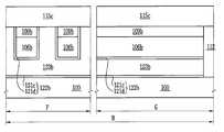
다른 실시예에서, 도 13에 도시된 바와 같이 상기 매립 패턴들(244) 사이에 위치하는 상기 연결부들(224a)은 생략될 수 있다. 따라서, 상기 매립 패턴들(244)의 각각은 서로 전기적으로 분리될 수 있다. 즉, 상기 각 매립 패턴들(244)에 독립적인 전기적 신호를 인가할 수 있다. 또한, 상기 매립 패턴들(244) 중 하나의 매립 패턴 상에 제공되는 활성 패턴들은 제1 도전형을 가질 수 있고, 상기 매립 패턴들(244) 중 다른 하나의 매립 패턴 상에 제공되는 활성 패턴들은 상기 제1 도전형과 다른 제2 도전형을 가질 수 있다. 상기 제1 도전형은 p형이고, 상기 제2 도전형은 n형일 수 있다. 따라서, 상기 매립 패턴들(244) 중 하나의 매립 패턴 상에 복수개의 NMOS 트랜지스터들이 제공되고, 상기 매립 패턴들(244) 중 다른 하나의 매립 패턴 상에 복수개의 PMOS 트랜지스터들이 제공될 수 있다. 상기 매립 패턴들(244)은 백 게이트 전극으로 이용할 수 있다. 따라서, 상기 매립 패턴들(244)의 각각은 전기적으로 분리될 수 있으므로, NMOS 트랜지스터들의 문턱전압을 제어하기 위한 제1 공통 백 게이트 전극이 제공될 수 있고, NMOS 트랜지스터들의 문턱전압을 제어하기 위한 제2 공통 백 게이트 전극이 제공될 수 있다.In another embodiment, as illustrated in FIG. 13, the connecting
따라서, 벌크 바디 소자와 아울러 플로팅 바디 소자를 갖는 시스템 온 칩(System On Chip)을 제공할 수 있다. 예를 들어, 본 발명의 일 실시예에서의 상 기 제1 내지 제3 소자 영역들(A, B, C)에 제공되는 소자들 중 하나 또는 둘 이상의 소자, 및 본 발명의 다른 실시예에서의 상기 제1 및 제2 소자 영역들(J, K)에 제공되는 소자들 중 하나 또는 둘의 소자가 하나의 칩 상에 구현될 수 있다. 또한, 앞에서 설명한 모든 소자들이 하나의 칩 상에 구현될 수도 있다.Accordingly, it is possible to provide a System On Chip having a bulk body element and a floating body element. For example, one or more of the elements provided in the first to third device regions A, B, and C in one embodiment of the present invention, and in another embodiment of the present invention. One or two of the devices provided in the first and second device regions J and K may be implemented on one chip. In addition, all the elements described above may be implemented on one chip.
이하에서, 상술한 본 발명의 실시예들에 따른 반도체소자들에 대한 제조방법들을 설명하기로 한다.Hereinafter, manufacturing methods for semiconductor devices according to the embodiments of the present invention described above will be described.
우선, 도 1a 내지 도 1h, 도 2a 내지 도 2c, 도 3a 내지 도 3c, 도 4a 내지 도 4c, 도 5a 내지 도 5c, 도 6a 내지 도 6c, 도 7a 내지 도 7c, 도 8a 내지 도 8c, 및 도 14를 참조하여 본 발명의 실시예들에 따른 반도체소자의 제조방법들을 설명하기로 한다.First, FIGS. 1A to 1H, 2A to 2C, 3A to 3C, 4A to 4C, 5A to 5C, 6A to 6C, 7A to 7C, and 8A to 8C, And the method of manufacturing a semiconductor device according to the embodiments of the present invention will be described with reference to FIG.
도 1a, 도 2a, 도 2b, 도 2c 및 도 14를 참조하면, 복수개의 소자 영역들을 갖는 기판(100)을 준비한다.(S100) 상기 기판(100)은 반도체 기판일 수 있다. 예를 들어, 상기 기판(100)은 실리콘 기판일 수 있다. 상기 기판(100)은 벌크 바디 소자영역과 플로팅 바디 소자영역들을 가질 수 있다. 상기 기판(100)은 상기 플로팅 바디 소자영역들 중의 제1 소자 영역(A), 상기 플로팅 바디 소자 영역들 중의 제2 소자 영역(B) 및 상기 플로팅 바디 소자 영역들 중의 제3 소자 영역(C)을 가질 수 있다. 상기 제1 소자 영역(A)은 제1 메모리 셀 어레이 영역이고, 상기 제2 소자 영역(B)은 제2 메모리 셀 어레이 영역이고, 상기 제3 소자 영역(C)은 제3 메모리 셀 어레이 영역일 수 있다. 그러나, 이에 한정되지 않는다. 예를 들어, 상기 제1 내지 제3 소자 영역들(A, B, C) 중 일부는 전계효과트랜지스터 영역들로 구성된 집적 회로 영역들일 수 있다.Referring to FIGS. 1A, 2A, 2B, 2C, and 14, a
한편, 상기 기판(100)의 벌크 바디 소자영역은 단면도 및 평면도로 도시하지 않았지만, 도 15에 개시된 공정 흐름도를 통하여 벌크 바디 소자영역에 형성하는 반도체소자를 같이 설명하기로 한다.On the other hand, although the bulk body device region of the
상기 제1 소자 영역(A)의 상기 기판(100) 상에 차례로 적층된 제1 희생막(102a) 및 제1 활성막(105a)을 형성할 수 있다. 상기 제1 희생막(102a) 및 상기 제1 활성막(105a)은 서로 다른 물질막들로 형성할 수 있다. 상기 제1 희생막(102a)은 상기 제1 활성막(105a)에 대하여 식각선택비를 갖는 물질막으로 형성할 수 있다. 예를 들어, 상기 제1 희생막(102a)은 에피택시얼 성장기술을 이용하여 실리콘 저마늄막(SiGe layer)으로 형성하고, 상기 제1 활성막(105a)은 에피택시얼 성장기술을 이용하여 실리콘막으로 형성할 수 있다. 따라서, 상기 제1 활성막(105a)은 단결정 구조의 실리콘막으로 형성할 수 있다.A first
이와 마찬가지로, 상기 제2 소자 영역(B)의 상기 기판(100) 상에 차례로 적층된 제2 희생막(102b) 및 제2 활성막(105b)을 형성할 수 있다. 또한, 상기 제3 소자 영역(C)의 상기 기판(100) 상에 차례로 적층된 제3 희생막(102c) 및 제3 활성막(105c)을 형성할 수 있다. 상기 제1 희생막들(102a, 102b, 102c)은 동일한 공정에 의해 형성된 동일한 두께를 갖는 물질로 형성할 수 있다. 상기 제2 활성막들(105a, 105b, 105c)은 동일한 공정에 의해 형성된 동일한 두께를 갖는 물질로 형성할 수 있다.Similarly, the second
다른 실시예에서, 상기 제1 희생막들(102a, 102b, 102c)은 서로 다른 두께를 갖도록 형성할 수 있다. 상기 제1 소자영역(A)의 상기 기판(100) 상에 제1 두께(t1)의 제1 희생막(102a)을 형성할 수 있다. 상기 제2 소자영역(B)의 상기 기판(100) 상에 상기 제1 두께(t1)와 다른 제2 두께(t2)의 제2 희생막(102b)을 형성할 수 있다. 상기 제3 소자영역(C)의 상기 기판(100) 상에 상기 제2 두께(t2)와 다른 제3 두께(t3)의 제3 희생막(102c)을 형성할 수 있다. 예를 들어, 상기 제1 내지 제3 소자영역들(A, B, C)을 갖는 상기 기판(100) 상에 희생막을 형성하고, 상기 제1 내지 제3 소자 영역들(A, B, C)에 형성할 소자들의 특성을 고려하여 상기 희생막을 적절히 식각하여 상기 제1 희생막(102a)을 상기 제1 두께(t1)로 형성하고, 상기 제2 희생막(102b)을 상기 제2 두께(t2)로 형성하고, 상기 제3 희생막(102c)을 상기 제3 두께(t3)로 형성할 수 있다.In another embodiment, the first
또 다른 실시예에서, 상기 제1 활성막들(105a, 105b, 105c)은 서로 다른 두께를 갖도록 형성할 수 있다. 상기 제1 희생막(102a) 상에 제4 두께(t4)의 제1 활성막(105a)을 형성할 수 있다. 상기 제2 희생막(102b) 상에 상기 제4 두께(t4)와 다른 제5 두께(t5)의 제2 활성막(105b)을 형성할 수 있다. 상기 제3 희생막(102c) 상에 상기 제5 두께(t5)와 다른 제6 두께(t6)의 제3 활성막(105c)을 형성할 수 있다. 예를 들어, 상기 제1 내지 제3 희생막들(102a, 102b, 102c)을 갖는 상기 기판(100) 상에 활성막을 형성한 후에, 상기 제1 내지 제3 소자 영역들(A, B, C) 중에서 적어도 하나의 영역 상에서의 상기 활성막의 두께를 부분적으로 낮추는 식각공정을 진행하여 서로 다른 두께를 갖는 상기 제1 내지 제3 활성막들(105a, 105b, 105c)을 형성할 수 있다.In another embodiment, the first
또 다른 실시예에서, 상기 제1 소자영역(A)의 상기 기판(100) 상에 제1 희생막(102a) 및 제1 활성막(105a)을 차례로 형성할 수 있다. 이때, 상기 제1 희생막(102a) 및 상기 제1 활성막(105a)을 차례로 형성하는 동안에, 상기 제2 및 제3 소자 영역들(B, C)은 하드 마스크에 의해 덮이고, 상기 제1 희생막(102a) 및 상기 제1 활성막(105a)을 형성한 후에, 상기 제2 및 제3 소자 영역들(B, C)을 덮는 하드 마스크를 제거할 수 있다. 이와 마찬가지로, 상기 제2 소자 영역(B)에 차례로 적층된 제2 희생막(102b) 및 제2 활성막(105b)을 형성하고, 상기 제3 소자영역(C)에 차례로 적층된 제3 희생막(102c) 및 제3 활성막(105c)을 형성할 수 있다. 이와 같이, 상기 제1 내지 제3 희생막들(102a, 102b, 102c)을 서로 다른 공정으로 형성하고, 상기 제1 내지 제3 활성막들(105a, 105b, 105c)을 서로 다른 공정으로 형성할 수 있다. 따라서, 상기 제1 내지 제3 희생막들(102a, 102b, 102c)을 서로 다른 두께를 갖도록 형성할 수 있고, 상기 제1 내지 제3 활성막들(105a, 105b, 105c)을 서로 다른 두께를 갖도록 형성할 수 있다. 또한, 상기 제1 내지 제3 활성막들(105a, 105b, 105c)을 서로 다른 원소를 포함하는 반도체 물질막들로 형성할 수도 있다.In another embodiment, the first
상기 제1 내지 제3 활성막들(105a, 105b, 105c)은 n형 또는 p형의 같은 도전형을 갖도록 형성할 수 있다. 이와는 달리, 상기 제1 내지 제3 활성막들(105a, 105b, 105c) 중 적어도 하나의 활성막은 제1 도전형이고, 나머지 활성막은 상기 제1 도전형과 다른 제2 도전형일 수 있다. 여기서, 상기 제1 도전형은 n형일 수 있다.The first to third
한편, 상기 제1 내지 제3 소자 영역들(A, B, C)에 상기 제1 내지 제3 희생막들(102a, 102b, 102c) 및 상기 제1 내지 제3 활성막들(105a, 105b, 105c)을 형성하는 동안에, 상기 기판(100)의 벌크 바디 소자영역은 희생마스크에 의해 보호될 수 있다. 상기 희생 마스크는 상기 제1 내지 제3 활성막들(105a, 105b, 105c)을 형성한 후에, 제거될 수 있다.Meanwhile, the first to third
도 1b, 도 3a, 도 3b, 도 3c 및 도 14를 참조하면, 상기 제1 소자 영역(A)의 상기 활성막(106) 상에 제1 하드 마스크 패턴(109a)을 형성하고, 상기 제2 소자 영역(B)의 상기 활성막(106) 상에 제2 하드 마스크 패턴(109b)을 형성하고, 상기 제3 소자 영역(C) 상의 상기 활성막(106) 상에 제3 하드 마스크 패턴(109c)을 형성할 수 있다.1B, 3A, 3B, 3C, and 14, a first
한편, 상기 벌크 소자 영역의 상기 기판(100) 상에 제4 하드 마스크 패턴을 형성할 수 있다.Meanwhile, a fourth hard mask pattern may be formed on the
상기 제1 내지 제3 하드 마스크 패턴들(109a, 109b, 109c)은 동일한 공정에 의해 형성될 수 있다. 상기 제1 내지 제3 하드 마스크 패턴들(109a, 109b, 109c)은 상기 제1 내지 제3 활성막들(105a, 105b, 105c)에 대하여 식각선택비를 갖는 물질로 형성할 수 있다. 예를 들어, 상기 제1 내지 제3 활성막들(105a, 105b, 105c)을 실리콘막으로 형성하는 경우에, 상기 제1 내지 제3 하드 마스크 패턴들(109a, 109b, 109c)은 실리콘 질화막을 포함하는 물질막으로 형성할 수 있다.The first to third
상기 제1 내지 제3 하드 마스크 패턴들(109a, 109b, 109c)을 식각마스크로 이용하여 상기 제1 내지 제3 활성막들(105a, 105b, 105c) 및 상기 제1 내지 제3 희 생막들(102a, 102b, 102c)을 차례로 식각하여 트렌치를 형성할 수 있다. 그 결과, 상기 제1 소자 영역(A)의 상기 기판(100) 상에 차례로 적층된 제1 희생 패턴(103a) 및 제1 활성 패턴(active pattern; 106a)이 하나 또는 복수개가 형성되고, 상기 제2 소자 영역(B)의 상기 기판(100) 상에 차례로 적층된 제2 희생 패턴(103b) 및 제2 활성 패턴(106b)이 하나 또는 복수개가 형성되고, 상기 제3 소자 영역(C)의 상기 기판(100) 상에 차례로 적층된 제3 희생 패턴(103c) 및 제3 활성 패턴(106c)이 하나 또는 복수개가 형성될 수 있다.Using the first to third
한편, 상기 제1 내지 제3 하드 마스크 패턴들(109a, 109b, 109c)을 식각마스크로 이용하여 상기 제1 내지 제3 활성막들(105a, 105b, 105c) 및 상기 제1 내지 제3 희생막들(102a, 102b, 102c)을 차례로 식각하는 동안에, 상기 기판(100)의 일부분이 식각될 수도 있다.Meanwhile, the first to third
한편, 상기 제1 내지 제3 하드 마스크 패턴들(109a, 109b, 109c)을 식각마스크로 이용하여 상기 제1 내지 제3 활성막들(105a, 105b, 105c) 및 상기 제1 내지 제3 희생막들(102a, 102b, 102c)을 차례로 식각하는 동안에, 상기 제4 하드 마스크 패턴을 이용하여 상기 벌크 바디 소자영역의 상기 기판(100)을 식각하여 활성 영역을 한정하는 트렌치를 형성할 수 있다.Meanwhile, the first to third
상기 트렌치를 채우는 제1 소자분리막(112)을 형성할 수 있다.(S110) 좀더 구체적으로, 상기 트렌치를 형성한 후에, 상기 트렌치를 갖는 상기 기판(100) 상에 절연막을 형성하고, 상기 제1 내지 제3 하드 마스크 패턴들(109a, 109b), 109c)의 상부면이 노출될 때까지 상기 절연막을 평탄화할 수 있다. 그 결과, 상기 트렌치를 채우는 상기 제1 소자분리막(112)이 형성될 수 있다. 상기 제1 소자분리막(112)은 상기 희생 패턴들(103a, 103b, 103c)에 대하여 식각선택비를 갖는 절연성 물질로 형성할 수 있다. 예를 들어, 상기 희생 패턴들(103a, 103b, 103c)을 실리콘 저마늄막으로 형성하는 경우에, 상기 제1 소자분리막(112)은 실리콘 산화막으로 형성할 수 있다. 따라서, 상기 제1 소자분리막(112)에 의해 상기 제1 내지 제3 소자 영역들(A, B, C) 상의 상기 제1 내지 제3 희생 패턴들(103a, 103b, 103c) 및 상기 제1 내지 제3 활성 패턴들(106a, 106b, 106c)이 한정됨과 아울러 상기 벌크 바디 소자영역의 상기 활성영역이 한정될 수 있다.(S110)A first
도 1c, 도 4a, 도 4b, 도 4c 및 도 14를 참조하면, 상기 제1 소자 영역(A) 상의 상기 제1 활성 패턴들(105a)을 가로지르는 적어도 하나의 개구부를 가지며 상기 제2 및 제3 소자 영역들(B, C), 및 상기 벌크 바디 소자영역을 덮는 제1 포토레지스트 패턴(115a)을 형성할 수 있다.1C, 4A, 4B, 4C, and 14, the second and second openings have at least one opening crossing the first
상기 제1 소자 영역(A)에서, 상기 제1 포토레지스트 패턴(115a)을 식각마스크로 이용하여 상기 제1 소자분리막(112)을 식각하여 상기 제1 희생 패턴들(103a)을 부분적으로 노출시키는 제1 리세스 영역들(112a)을 형성할 수 있다.(S120) 예를 들어, 상기 제1 소자 영역(A)의 상기 제1 리세스 영역들(112a)은 상기 차례로 적층된 상기 제1 희생 패턴들(103a) 및 상기 활성 패턴들(106a) 각각의 측벽의 일부분을 노출시킬 수 있다. 그 결과, 상기 제1 리세스 영역들(112a)에 의해 상기 제1 활성 패턴들(106a)의 노출되지 않은 측벽들은 상기 소자분리막(112)과 접촉할 수 있다. 이어서, 상기 제1 활성 패턴들(106a) 하부의 상기 제1 희생 패턴들(103a)을 선 택적으로 제거하여 상기 제1 활성 패턴들(106a)과 상기 기판(100) 사이에 빈 공간들(118a)을 형성할 수 있다.(S130) 상기 제1 희생 패턴들(103a)을 제거하는 것은 습식 식각공정을 이용할 수 있다. 여기서, 상기 제1 빈 공간들(118a)에 의해 상기 기판(100)으로부터 이격된 상기 제1 활성 패턴들(106a)은 상기 소자분리막(112)의 리세스 되지 않은 부분과 접촉함으로써 지지될 수 있다.In the first device region A, the first
도 1d, 도 5a, 도 5b, 도 5c 및 도 14를 참조하면, 상기 제1 포토레지스트 패턴(115a)을 제거할 수 있다. 상기 제1 소자 영역(A)에서, 상기 제1 빈 공간들(도 4a의 118a) 및 상기 제1 리세스 영역들(도 4a의 112a)에 의해 노출된 상기 기판(100) 및 상기 제1 활성 패턴들(106a)에 상기 제1 매립 유전막(122a)을 형성할 수 있다.(S140) 상기 제1 매립 유전막(122a)은 상기 제1 빈 공간(도 4a의 118a) 및 상기 제1 리세스 영역(도 4a의 112a)에 의해 노출된 상기 기판(100)에 형성된 제1 하부 매립 유전막(121a)과, 상기 제1 빈 공간(도 4a의 118a) 및 상기 제1 리세스 영역(도 4a의 112a)에 의해 노출된 상기 제1 활성 패턴들(106a)에 형성된 제1 상부 매립 유전막(121b)으로 구성될 수 있다. 상기 제1 매립 유전막(122a)은 실리콘 산화막 또는 실리콘산화막보다 유전상수가 큰 고유전막(high-k dielectric layer)으로 형성할 수 있다.1D, 5A, 5B, 5C, and 14, the
한편, 상기 제1 매립 유전막(122a)은 정보 저장 물질막을 포함하도록 형성할 수 있다. 상기 정보 저장 물질막은 플래쉬 메모리 소자의 전하 저장층일 수 있다. 예를 들어, 상기 제1 매립 유전막(122a)은 제1 산화막, 전하 저장층으로서의 질화막 및 제2 산화막으로 이루어진 ONO막으로 형성할 수 있다. 한편, 상기 정보 저장 물질막으로서 나노 크리스탈(nano crystal) 물질을 이용할 수도 있다.The first buried
상기 제1 매립 유전막(122a)을 갖는 기판 상에 상기 제1 빈 공간들(도 4a의 118a)을 채움과 아울러 적어도 상기 제1 리세스 영역들(도 4a의 112a)의 하부 영역을 채우는 제1 매립막(123a)을 형성할 수 있다. 바람직하게는, 상기 제1 매립막(123a)은 상기 제1 빈 공간들(도 4a의 118a)을 채움과 아울러 상기 제1 리세스 영역들(도 4a의 112a)을 채우도록 형성할 수 있다. 상기 제1 매립막(123a)을 형성하는 것은 상기 제1 매립 유전막(122a)을 갖는 기판 상에 매립 특성이 우수한 물질막을 형성하고, 상기 제1 내지 제3 하드 마스크 패턴들(109a, 109b, 109c)이 노출될 때까지 상기 물질막을 평탄화하는 것을 포함할 수 있다.A first filling the first
상기 제1 매립막(123a)은 n형 도우프트 반도체 물질막, p형 도우프트 반도체 물질막, 언도우프트(undoped) 반도체물질막 또는 금속 물질막으로 형성할 수 있다. 상기 반도체물질막은 실리콘막일 수 있고, 상기 금속 물질막은 타이타늄 질화막(TiN layer) 또는 탄탈륨 질화막(TaN layer)일 수 있다.The first buried
상기 제2 소자 영역(B) 상의 상기 제2 활성 패턴들(105b)을 가로지르는 적어도 하나의 개구부를 가지며 상기 제1 및 제3 소자 영역들(A, C)을 덮는 제2 포토레지스트 패턴(115a)을 형성할 수 있다. 상기 제1 소자 영역(A)에서 상기 제1 리세스 영역들(도 4a의 112a)과 상기 제1 빈 공간들(도 4a의 118a)을 형성하는 것과 실질적으로 동일한 방법을 사용하여 상기 제2 소자 영역(B)에 제2 리세스 영역들(112b) 및 제2 빈 공간들(118b)을 형성할 수 있다.(S120, S130) 즉, 상기 제2 빈 공간들(118b)은 상기 제2 희생막(도 4b의 103b)이 제거된 공간일 수 있다.The
도 1e, 도 6a, 도 6b, 도 6c 및 도 14를 참조하면, 상기 제2 포토레지스트 패턴(115b)을 제거할 수 있다. 상기 제1 매립 유전막(122a) 및 상기 제1 매립막(123a)을 형성하는 것과 실질적으로 동일한 방법을 이용하여 제2 매립 유전막(122b) 및 제2 매립막(123b)을 형성할 수 있다. 좀더 구체적으로, 상기 제2 소자 영역(B)의 상기 제2 빈 공간들(도 5b의 118b) 및 상기 제2 리세스 영역들(도 5b의 112b)에 의해 노출된 상기 기판(100) 및 상기 제2 활성 패턴들(106b)에 상기 제2 매립 유전막(122b)을 형성할 수 있다.(S140) 상기 제2 매립 유전막(122b)은 상기 제2 빈 공간(도 5b의 118b) 및 상기 제2 리세스 영역(도 5b의 112b)에 의해 노출된 상기 기판(100)에 형성된 제2 하부 매립 유전막(121c)과 상기 제2 빈 공간(도 5b의 118b) 및 상기 제2 리세스 영역(도 5b의 112b)에 의해 노출된 상기 제2 활성 패턴들(106b)에 형성된 제2 상부 매립 유전막(121d)으로 구성될 수 있다. 상기 제2 매립 유전막(122b)은 상기 제1 매립 유전막(122a)과 다른 두께를 갖도록 형성할 수 있다. 또한, 상기 제2 매립 유전막(122b)은 상기 제1 매립 유전막(122a)과 다른 물질을 포함하도록 형성할 수 있다.1E, 6A, 6B, 6C, and 14, the
한편, 상기 제2 매립 유전막(122b)은 정보 저장 물질막을 포함하도록 형성할 수 있다.The second buried
상기 제2 매립 유전막(122b)을 갖는 기판 상에 상기 제2 빈 공간들(도 5b의 118b)을 채움과 아울러 상기 제2 리세스 영역들(도 5b의 112b)을 채우는 제2 매립막(123b)을 형성할 수 있다. 상기 제2 매립막(123b)은 상기 제1 매립막(123a)과 동일한 물질로 형성할 수 있다.The second buried
한편, 상기 제2 매립막(123b)은 상기 제1 매립막(123a)과 다른 특성을 갖도록 형성할 수 있다. 예를 들어, 상기 제1 매립막(123a)을 제1 도전형의 실리콘막으로 형성하는 경우에, 상기 제2 매립막(123b)은 언도우프트 실리콘막 또는 상기 제1 도전형과 다른 제2 도전형의 실리콘막으로 형성할 수 있다. 상기 제1 도전형은 n형 또는 p형 일 수 있다. 이와는 달리, 상기 제1 매립막(123a)을 언도우프트 실리콘막으로 형성하는 경우에, 상기 제2 매립막(123b)을 n형 또는 p형의 도우프트 실리콘막으로 형성할 수도 있다.The second buried
상기 제3 소자 영역(C) 상의 상기 제3 활성 패턴들(105c)을 가로지르는 적어도 하나의 개구부를 가지며 상기 제1 및 제2 소자 영역들(A, B)을 덮는 제3 포토레지스트 패턴(115c)을 형성할 수 있다. 상기 제2 소자 영역(B)에서 상기 제2 리세스 영역들(도 5b의 112b)과 상기 제2 빈 공간들(도 5b의 118b)을 형성하는 것과 실질적으로 동일한 방법을 사용하여 상기 제3 소자 영역(C)에 제3 리세스 영역들(112c) 및 제3 빈 공간들(118c)을 형성할 수 있다.(S120, S130) 즉, 상기 제3 빈 공간들(118c)은 상기 제3 희생막(도 5c의 103c)이 제거된 공간일 수 있다.
도 1f, 도 7a, 도 7b, 도 7c 및 도 14를 참조하면, 상기 제3 포토레지스트 패턴(115c)을 제거할 수 있다. 상기 제2 매립 유전막(122b) 및 상기 제2 매립막(123b)을 형성하는 것과 실질적으로 동일한 방법을 이용하여 제3 매립 유전막(122c) 및 제3 매립막(123c)을 형성할 수 있다. 좀더 구체적으로, 상기 제3 소자 영역(C)의 상기 제3 빈 공간들(도 6c의 118c) 및 상기 제3 리세스 영역들(도 6c의 112c)에 의해 노출된 상기 기판(100) 및 상기 제3 활성 패턴들(106c)에 상기 제3 매립 유전막(122c)을 형성할 수 있다.(S140) 상기 제3 매립 유전막(122c)은 상기 제3 빈 공간(도 6c의 118c) 및 상기 제3 리세스 영역(도 6c의 112c)에 의해 노출된 상기 기판(100)에 형성된 제3 하부 매립 유전막(121f)과 상기 제3 빈 공간(도 6c의 118c) 및 상기 제3 리세스 영역들(도 6c의 112c)에 의해 노출된 상기 제3 활성 패턴들(106c)에 형성된 제3 상부 매립 유전막(121e)으로 구성될 수 있다. 상기 제3 매립 유전막(122c)은 상기 제2 매립 유전막(122b)과 다른 물질막을 포함하도록 형성할 수 있다. 한편, 상기 제3 매립 유전막(122c)은 정보 저장 물질막을 포함하도록 형성할 수 있다.1F, 7A, 7B, 7C, and 14, the
상기 제3 매립 유전막(122c)을 갖는 기판 상에 상기 제3 빈 공간들(도 6c의 118c)을 채움과 아울러 상기 제3 리세스 영역들(도 6c의 112c)을 채우는 제3 매립막(123c)을 형성할 수 있다. 상기 제3 매립막(123c)은 상기 제2 매립막(123b)과 다른 특성을 갖도록 형성할 수 있다. 예를 들어, 상기 제2 매립막(123a)을 제1 도전형의 실리콘막으로 형성하는 경우에, 상기 제3 매립막(123c)은 언도우프트 실리콘막 또는 상기 제1 도전형과 다른 제2 도전형의 실리콘막으로 형성할 수 있다. 이와는 달리, 상기 제2 매립막(123b)을 언도우프트 실리콘막으로 형성하는 경우에, 상기 제3 매립막(123a)을 n형 또는 p형의 도우프트 실리콘막, 또는 금속물질막으로 형성할 수도 있다.The third
따라서, 상기 제1 내지 제3 매립 유전막들(122a, 122b, 122c)은 서로 다른 물질을 포함하도록 형성할 수 있다. 이와 마찬가지로, 상기 제1 내지 제3 매립막들(123a, 123b, 123c)은 서로 다른 특성의 물질을 포함하도록 형성할 수 있다.Therefore, the first to third buried
다른 실시예에서, 상기 제1 내지 제3 포토레지스트 패턴들(115a, 115b, 115c) 대신에 하드 마스크 패턴들을 이용할 수도 있다.In another embodiment, hard mask patterns may be used instead of the first to
또 다른 실시예에서, 도 5a 내지 도 5c에서 설명한 공정, 도 6a 내지 도 6c에서 설명한 공정 및 상기 도 7a 내지 도 7c에서 설명한 공정은 동시에 진행될 수 있다. 예를 들어, 도 5a 내지 도 5c에서 설명한 상기 제1 포토레지스터 패턴(115a) 대신에, 상기 제1 소자 영역(A)의 상기 제1 활성 패턴들(106a)을 가로지르는 개구부, 상기 제2 소자 영역(B)의 상기 제2 활성 패턴들(106b)을 가로지르는 다른 개구부 및 상기 제3 소자 영역(C)의 상기 제3 활성 패턴들(106c)을 가로지르는 또 다른 개구부를 갖는 포토레지스트 패턴을 형성하고, 상기 포토레지스트 패턴을 식각마스크로 이용하여 상기 개구부들에 의해 노출된 상기 소자분리막(112)을 부분식각하여 상기 제1 내지 제3 리세스 영역들(도 4a의 112a, 도 5b의 112b, 도 6c의 112c)을 동시에 형성하고 상기 포토레지스트 패턴을 제거할 수 있다.(S120) 또한, 상기 제1 내지 제3 희생 패턴들(103a, 103b, 103c)을 동시에 제거하여 상기 제1 내지 제3 빈 공간들(도 4a의 118a, 도 5b의 118b, 도 6c의 118c)을 동시에 형성할 수 있다.(S130) 따라서, 상기 제1 내지 제3 매립 유전막들(122a, 122b, 122c)을 동시에 형성할 수 있고, 상기 제1 내지 제3 매립막들(123a, 123b, 123c)을 동시에 형성할 수 있다.In another embodiment, the process described with reference to FIGS. 5A through 5C, the process described with reference to FIGS. 6A through 6C, and the process described with reference to FIGS. 7A through 7C may be simultaneously performed. For example, instead of the
도 1g, 도 8a, 도 8b, 도 8c 및 도 14를 참조하면, 상기 제1 소자 영역(A)에서, 상기 제1 매립막(도 7a의 123a)을 식각하여 상기 제1 활성 패턴들(106a) 하부에 자기정렬된 제1 매립 패턴들(124a)을 형성할 수 있다.(S150) 따라서, 상기 제1 매립 패턴들(124a)은 서로 이격될 수 있다.1G, 8A, 8B, 8C, and 14, in the first device region A, the first buried
상기 제2 소자 영역(B)에서, 상기 제2 매립막(도 7b의 123b)을 부분식각하여 상기 제2 활성 패턴들(106b) 하부에 자기정렬된 제2 매립 패턴들(124b)을 형성함과 아울러 상기 제2 매립 패턴들(124b)을 연결하는 적어도 하나의 제1 연결부(125b)를 형성할 수 있다.(S150) 상기 제1 연결부(125b)는 상기 제2 매립 패턴들(124b)과 실질적으로 동일한 레벨에 위치할 수 있다. 상기 제1 연결부(125b)가 복수개가 형성되는 경우에, 평면도로 보았을 때, 상기 제1 연결부들(125b)은 도 1g에 도시된 바와 같이 서로 이격되어 상기 제2 매립 패턴들(124b)을 연결할 수 있다.In the second device region B, second buried
상기 제3 소자 영역(C)에서, 상기 제3 매립막(도 7c의 123c)을 부분식각하여 상기 제3 활성 패턴들(106c) 하부에 자기정렬된 제3 매립 패턴들(124c)을 형성함과 아울러 상기 제3 매립 패턴들(124c)을 연결하는 적어도 하나의 제2 연결부(125c)를 형성할 수 있다.(S150) 여기서, 상기 제2 연결부(125c)는 상기 제3 매립 패턴들(124c)을 서로 연결하며 상기 제3 활성 패턴들(106c)의 측벽들을 덮도록 형성할 수 있다. 이때, 상기 제3 활성 패턴들(106)의 측벽들과 상기 제2 연결부(125c)는 상기 제3 매립 유전막(122c)의 두께만큼 이격될 수 있다. 상기 제2 연결부(125c)가 복수개가 형성되는 경우에, 평면도로 보았을 때, 상기 제2 연결부들(125c)은 도 1g에 도시된 바와 같이 서로 이격되어 상기 제3 매립 패턴들(124c)을 연결할 수 있다.In the third device region C, the third buried
이어서, 상기 제1 내지 제3 매립막들(도 7a 내지 도 7c의 123a, 123b, 123c)을 식각하므로써 형성된 리세스 영역을 채우는 제2 소자분리막(127)을 형성할 수 있다. 상기 제2 소자분리막(127)은 절연성 물질로 형성할 수 있다. 예를 들어, 상기 제2 소자분리막(127)은 실리콘 산화막으로 형성할 수 있다.Subsequently, the second
이제, 도 1h, 도 9a 내지 도 9c, 도 10a 내지 도 10c 및 도 14를 참조하여, 상술한 상기 1 내지 제3 매립 패턴들(123a, 123b, 123c)을 갖는 상기 제1 내지 제3 소자 영역들(A, B, C)에 다양한 게이트 구조 및 배선 구조의 반도체소자를 제조하는 방법을 설명하기로 한다.Now, the first to third device regions having the first to third
도 1h, 도 9a, 도 9b, 도 9c 및 도 14를 참조하면, 상기 제1 소자 영역(A)에서, 상기 제1 활성 패턴들(106a)의 소정 영역들을 제거할 수 있다. 예를 들어, 사진 및 식각공정을 이용하여, 후에 형성할 하부 게이트 콘택 구조체를 형성하기 위한 영역과 중첩하는 상기 제1 활성 패턴들(106a)의 소정 영역들을 제거할 수 있다.1H, 9A, 9B, 9C, and 14, in the first device region A, predetermined regions of the first
상기 제1 소자 영역(A)에서, 상기 제1 마스크 패턴들(도 8a의 109a)을 제거하고, 상기 제1 활성 패턴들(106a) 상에 차례로 적층된 제1 게이트 구조체(136a) 및 제1 게이트 마스크 패턴(139a)을 하나 또는 복수개 형성할 수 있다.(S160) 상기 제1 게이트 구조체들(136a)의 각각은 차례로 적층된 제1 게이트 유전막(130a) 및 제1 게이트 전극(133a)을 포함할 수 있다.In the first device region A, the
한편, 상기 제1 활성 패턴들(106a)의 각각에 복수개의 제1 게이트 구조체들(136a)이 형성될 수 있다. 즉, 상기 제1 게이트 구조체들(136a)은 상기 제1 활성 패턴들(106a) 상에 아일랜드 형으로 형성할 수 있다.Meanwhile, a plurality of
상기 제1 게이트 유전막(130a)은 실리콘 산화막 또는 상기 실리콘 산화막보 다 높은 유전상수를 갖는 고유전막으로 형성할 수 있다. 상기 제1 게이트 전극(133a)은 도전성 물질막으로 형성할 수 있다.The first
한편, 상기 제1 게이트 유전막(130a)은 상기 제1 매립 유전막(122a)과 동일한 물질로 형성할 수 있다. 예를 들어, 상기 제1 매립 유전막(122a)을 정보 저장 물질막을 포함하는 유전체로 형성하고, 상기 제1 게이트 유전막(130a)을 상기 제1 매립 유전막(122a)과 동일한 물질로 형성하는 경우에, 상기 제1 소자 영역(A)은 멀티 비트, 예를 들어 4 비트 저장 노드를 갖는 플래쉬 메모리 소자의 셀 영역으로 이용할 수 있다. 또한, 상기 제1 게이트 유전막(130a)과 상기 제1 매립 유전막(122a)을 서로 동일한 물질로 형성함과 아울러 서로 같은 두께로 형성하는 경우에, 동일한 동작 전압에 의해 프로그래밍/소거/읽기 동작이 이루어질 수 있다.The first
상기 제1 게이트 마스크 패턴들(139a)은 절연성 물질로 형성할 수 있다. 예를 들어, 상기 제1 게이트 마스크 패턴들(139a)은 실리콘 산화막 및 실리콘 질화막 중 적어도 하나를 포함하도록 형성할 수 있다.The first
상기 제2 소자 영역(B)에서, 상기 제2 활성 패턴들(106b)의 소정 영역들을 제거할 수 있다. 예를 들어, 사진 및 식각공정을 이용하여, 후에 형성할 하부 게이트 콘택 구조체를 형성하기 위한 영역과 중첩하는 상기 제2 활성 패턴들(106b)의 소정 영역들을 제거할 수 있다. 상기 제2 소자 영역(B)에서, 상기 제2 마스크 패턴들(도 8b의 109b)을 제거하고, 상기 제2 활성 패턴들(106b) 상에 차례로 적층된 제2 게이트 구조체들(136b) 및 제2 게이트 마스크 패턴들(139b)을 형성할 수 있다.(S160) 상기 제2 게이트 구조체들(136b)의 각각은 차례로 적층된 제2 게이트 유 전막(130b) 및 제2 게이트 전극(133b)을 포함할 수 있다. 상기 제2 게이트 유전막(130b)은 상기 제1 게이트 유전막(130a)과 같은 유전막으로 형성하거나, 다른 유전막으로 형성할 수 있다.In the second device region B, predetermined regions of the second
한편, 상기 제2 게이트 구조체들(136b)은 상기 제2 활성 패턴들(106b)의 측벽들 중 적어도 하나의 측벽을 덮도록 형성할 수 있다. 더 나아가, 상기 제2 게이트 구조체들(136b)은 상기 제2 활성 패턴들(106b)의 상부면을 덮도록 형성할 수 있다. 여기서, 상기 제2 게이트 구조체들(136b)이 상기 제2 활성 패턴들(106b)의 측벽들 중 적어도 하나의 측벽을 덮게 하기 위하여, 상기 제2 게이트 구조체들(136b)을 형성하기 전에, 사진 및 식각공정을 이용하여 상기 제2 활성 패턴들(106b)에 인접한 상기 제2 소자분리막(117)을 식각하여 상기 제2 활성 패턴들(106b)의 측벽들을 노출시키는 리세스 영역을 형성할 수 있다.The
상기 제2 게이트 유전막(130b)은 실리콘 산화막 또는 상기 실리콘 산화막보다 높은 유전상수를 갖는 고유전막으로 형성할 수 있다. 상기 제2 게이트 전극(133b)은 도전성 물질막으로 형성할 수 있다. 한편, 상기 제2 게이트 유전막(130b)은 정보 저장 물질막을 포함하도록 형성할 수 있다.The second
한편, 상기 제2 게이트 유전막(130b)은 상기 제2 매립 유전막(122b)과 동일한 물질로 형성할 수 있다.The second
상기 제2 게이트 마스크 패턴들(139b)은 절연성 물질로 형성할 수 있다. 예를 들어, 상기 제2 게이트 마스크 패턴들(139b)은 실리콘 산화막 및 실리콘 질화막 중 적어도 하나를 포함하도록 형성할 수 있다. The second
상기 제3 소자 영역(B)에서, 상기 제3 활성 패턴들(106c)의 소정 영역들을 제거할 수 있다. 예를 들어, 사진 및 식각공정을 이용하여, 후에 형성할 하부 게이트 콘택 구조체를 형성하기 위한 영역과 중첩하는 상기 제3 활성 패턴들(106c)의 소정 영역들을 제거할 수 있다. 상기 제3 소자 영역(C)에서, 상기 제3 마스크 패턴들(도 8c의 109c)을 제거하고, 상기 제3 활성 패턴들(106c) 상에 차례로 적층된 제3 게이트 구조체들(136c) 및 제3 게이트 마스크 패턴들(139c)을 형성할 수 있다.(S160) 상기 제3 게이트 구조체들(136c)의 각각은 차례로 적층된 제3 게이트 유전막(130c) 및 제3 게이트 전극(133c)을 포함할 수 있다. 상기 제3 게이트 유전막(130c)은 상기 제1 및 제2 게이트 유전막들(130a, 130b)과 같은 유전막으로 형성하거나, 다른 유전막으로 형성할 수 있다.In the third device region B, predetermined regions of the third
상기 제3 게이트 유전막(130c)은 실리콘 산화막 또는 상기 실리콘 산화막보다 높은 유전상수를 갖는 고유전막으로 형성할 수 있다. 상기 제3 게이트 전극(133c)은 도전성 물질막으로 형성할 수 있다. 한편, 상기 제3 게이트 유전막(130c)은 정보 저장 물질막을 포함하도록 형성할 수 있다. 상기 제3 게이트 마스크 패턴들(139c)은 절연성 물질로 형성할 수 있다.The third
한편, 상기 제3 게이트 유전막(130c)은 상기 제3 매립 유전막(122c)과 동일한 물질로 형성할 수 있다.The third
다른 실시예에서, 상기 제1 내지 제3 마스크 패턴들(도 8a 내지 도 8c의 109a, 109b, 109c)을 동시에 제거하여 상기 제1 내지 제3 활성 패턴들(106a, 106b, 106c)을 노출시키고, 상기 제1 활성 패턴들(106a) 상에 제1 게이트 유전막(130a)을 형성하고, 상기 제2 활성 패턴들(106b) 상에 제2 게이트 유전막(130b)을 형성하고, 상기 제3 활성 패턴들(106c) 상에 제3 게이트 유전막(130c)을 형성할 수 있다. 이후, 상기 제1 게이트 유전막(130a) 상에 차례로 적층된 제1 게이트 전극(133a) 및 제1 게이트 마스크 패턴(139a)을 형성하고, 상기 제2 게이트 유전막(130b) 상에 차례로 적층된 제2 게이트 전극(133b) 및 제2 게이트 마스크 패턴(139b)을 형성하고, 상기 제3 게이트 유전막(130c) 상에 차례로 적층된 제3 게이트 전극(133c) 및 제3 게이트 마스크 패턴(139c)을 형성할 수 있다.(S160)In another embodiment, the first to third mask patterns (109a, 109b and 109c of FIGS. 8A to 8C) may be simultaneously removed to expose the first to third
한편, 상기 제1 내지 제3 게이트 구조체들(136a, 136b, 136c)을 형성하는 동안에, 상기 벌크 바디 소자 영역에서, 상기 활성 영역 상의 상기 제4 하드 마스크 패턴을 제거하고, 상기 활성 영역 상에 제4 게이트 구조체를 형성할 수 있다.(S160) 이때의 상기 제4 게이트 구조체는 차례로 적층된 제4 게이트 유전막 및 제4 게이트 전극을 포함할 수 있다.Meanwhile, during the formation of the first to
본 발명에서, 상기 제1 내지 제3 활성 패턴들(106a, 106b, 106c)의 두께들을 제어할 수 있다고 설명한 바 있다. 따라서, 상기 제1 내지 제3 활성 패턴들(106a, 106b, 106c)의 두께들을 조절하여 완전 공핍(fully depleted) 또는 부분 공핍(partially depleted) 트랜지스터들을 형성할 수 있다. 즉, 보다 다양한 반도체 회로를 설계할 수 있도록, 다양한 특성의 트랜지스터들을 제공할 수 있다.In the present invention, it has been described that the thicknesses of the first to third
상기 차례로 적층된 상기 제1 게이트 구조체들(136a) 및 상기 제1 게이트 마스크 패턴들(139a)의 측벽들 상에 제1 게이트 스페이서들(142a)을 형성할 수 있다. 상기 차례로 적층된 상기 제2 게이트 구조체들(136b) 및 상기 제2 게이트 마스크 패턴들(139b)의 측벽들 상에 제2 게이트 스페이서들(142b)을 형성할 수 있다. 상기 차례로 적층된 상기 제3 게이트 구조체들(136c) 및 상기 제3 게이트 마스크 패턴들(139c)의 측벽들 상에 제3 게이트 스페이서들(142c)을 형성할 수 있다. 상기 제1 내지 제3 게이트 스페이서들(142a, 142b, 142c)은 동시에 형성할 수 있다. 상기 제1 내지 제3 게이트 스페이서들(142a, 142b, 142c)은 절연성 물질로 형성할 수 있다. 예를 들어, 상기 제1 내지 제3 게이트 스페이서들(142a, 142b, 142c)은 실리콘 산화막 및 실리콘 질화막 중 적어도 하나를 포함하도록 형성할 수 있다.
상기 제1 게이트 구조체들(136a) 양 옆의 상기 제1 활성 패턴들(106b)에 제1 소스/드레인 영역들(145a)을 형성할 수 있다. 예를 들어, 상기 제1 게이트 구조체들(136a)의 양 옆의 상기 제1 활성 패턴들(106a)에 상기 제1 활성 패턴들(106a)과 다른 도전형을 갖는 불순물 이온들을 주입하여 상기 제1 소스/드레인 영역들(145a)을 형성할 수 있다. 상기 제1 소스/드레인 영역들(145a) 사이에 위치하는 상기 제1 활성 패턴들(106a)은 트랜지스터의 채널 영역으로 정의될 수 있다.First source /
상기 제2 게이트 구조체들(136b) 양 옆의 상기 제2 활성 패턴들(106b)에 제2 소스/드레인 영역들(145b)을 형성할 수 있다. 예를 들어, 상기 제2 게이트 구조체들(136b)의 양 옆의 상기 제2 활성 패턴들(106b)에 상기 제2 활성 패턴들(106b)과 다른 도전형을 갖는 불순물 이온들을 주입하여 상기 제2 소스/드레인 영역들(145b)을 형성할 수 있다.Second source /
상기 제3 게이트 구조체들(136c) 양 옆의 상기 제3 활성 패턴들(106c)에 제3 소스/드레인 영역들(145c)을 형성할 수 있다. 예를 들어, 상기 제3 게이트 구조체 들(136c) 양 옆의 상기 제3 활성 패턴들(106c)에 상기 제3 활성 패턴들(106c)과 다른 도전형을 갖는 불순물 이온들을 주입하여 상기 제3 소스/드레인 영역들(145c)을 형성할 수 있다.Third source /
한편, 상기 제3 소자 영역(C)에 플로팅 바디 디램(floating body DRAM) 셀 어레이를 형성한다면, 상기 제3 소스/드레인 영역들(145c) 사이의 상기 제3 활성 패턴(106c)은 정보 저장 영역으로 정의될 수 있다.Meanwhile, when a floating body DRAM cell array is formed in the third device region C, the third
상기 제1 내지 제3 소스/드레인 영역들(145a, 145b, 145c)을 갖는 기판 상에 하부 층간절연막(147)을 형성할 수 있다. 상기 하부 층간절연막(147)은 실리콘 산화막 또는 저유전막(low-k dielectric layer)으로 형성할 수 있다.A lower
도 1h, 도 10a, 도 10b, 도 10c 및 도 15를 참조하면, 상기 제1 소자 영역(A)에서, 상기 하부 층간절연막(147)을 패터닝하여 상기 제1 활성 패턴들(106a)을 가로지르며 상기 제1 소스/드레인 영역들(145a)을 노출시키는 라인 형태의 제1 트렌치들을 형성하고, 상기 제1 트렌치들을 채우는 라인 형태의 제1 하부 도전성 패턴들(148)을 형성할 수 있다. 따라서, 상기 제1 하부 도전성 패턴들(148)은 상기 하부 층간절연막(147)을 관통하며 상기 제1 소스/드레인 영역들(145a)과 전기적으로 접속할 수 있다. 상기 제1 하부 도전성 패턴들(148)의 각각은 상기 제1 게이트 전극들(133a) 사이에 위치하며 상기 제1 게이트 마스크 패턴들(139a)과 상기 제1 게이트 스페이서들(142a)에 의해 상기 제1 게이트 전극들(133a)과 이격될 수 있다. 상기 제1 소자 영역(A)에 메모리 소자의 셀 어레이를 형성할 경우, 상기 제1 하부 도전성 패턴들(148)은 비트라인들로 정의할 수 있다.1H, 10A, 10B, 10C, and 15, in the first device region A, the lower
상기 제2 소자 영역(B)에서, 상기 하부 층간절연막(147)을 패터닝하여 상기 제2 활성 패턴들(106b)을 가로지르며 상기 제2 소스/드레인 영역들(145b) 중 하나를 노출시키는 라인 형태의 제2 트렌치들을 형성함과 아울러 상기 제2 소스/드레인 영역들(145b) 중 다른 하나를 노출시키는 제2 콘택 홀들을 형성하고, 상기 제2 트렌치들을 채우는 제2 하부 도전성 패턴들(149a)을 형성함과 아울러 상기 제2 콘택 홀들을 채우는 제2 하부 콘택 구조체들(149b)을 형성할 수 있다. 따라서, 상기 제2 하부 도전성 패턴들(149a)은 상기 제2 소스/드레인 영역들(145b) 중 하나와 전기적으로 접속하고, 상기 제2 하부 콘택 구조체들(149b)은 상기 제2 소스/드레인 영역들(145b) 중 다른 하나와 전기적으로 접속할 수 있다. 도 1h에 도시된 바와 같이, 상기 제2 하부 도전성 패턴들(149a)은 복수개의 상기 제2 활성 패턴들(106b)을 가로지르는 라인 형태로 형성하고, 상기 제2 하부 콘택 구조체들(149b)은 아일랜드형으로 형성할 수 있다.In the second device region B, the lower
상기 제3 소자 영역(C)에서, 상기 하부 층간절연막(147)을 패터닝하여 상기 제3 활성 패턴들(106c)을 가로지르며 상기 제3 소스/드레인 영역들(145c) 중 하나를 노출시키는 라인 형태의 제3 트렌치들을 형성함과 아울러 상기 제3 소스/드레인 영역들(145c) 중 다른 하나를 노출시키는 제3 콘택 홀들을 형성하고, 상기 제3 트렌치들을 채우는 제3 하부 도전성 패턴들(150a)을 형성함과 아울러 상기 제3 콘택 홀들을 채우는 제3 하부 콘택 구조체들(150b)을 형성할 수 있다. 따라서, 상기 제3 하부 도전성 패턴들(150a)은 상기 제3 소스/드레인 영역들(145c) 중 하나와 전기적으로 접속하고, 상기 제3 하부 콘택 구조체들(150b)은 상기 제3 소스/드레인 영역 들(145c) 중 다른 하나와 전기적으로 접속할 수 있다. 도 1h에 도시된 바와 같이, 상기 제3 하부 도전성 패턴들(150a)은 복수개의 상기 제3 활성 패턴들(106c)을 가로지르는 라인 형태로 형성하고, 상기 제3 하부 콘택 구조체들(150b)은 아일랜드형으로 형성할 수 있다.In the third device region C, the lower
한편, 상기 제1 내지 제3 하부 도전성 패턴들(148, 149a, 150a), 제2 및 제3 하부 콘택 구조체들(149b, 150b)은 동시에 형성할 수 있다.Meanwhile, the first to third lower
이어서, 상기 제1 내지 제3 하부 도전성 패턴들(148, 149a, 150a), 상기 제2 및 제3 하부 콘택 구조체들(149b, 150b)을 갖는 기판 상에 상부 층간절연막(151)을 형성할 수 있다. 상기 상부 층간절연막(151)은 실리콘 산화막으로 형성할 수 있다.Subsequently, an upper
상기 제1 소자 영역(A)에서, 상기 상부 층간절연막(151)을 관통하며 상기 제1 게이트 전극들(133a)과 전기적으로 접속된 제1 게이트 콘택 구조체들(154a)을 형성할 수 있다. 이어서, 상기 상부 층간절연막(151) 상에 상기 제1 활성 패턴들(106a)과 교차하는 방향성을 가지며 상기 제1 게이트 콘택 구조체들(154a)을 덮는 라인 형태의 제1 상부 도전성 라인들(157a)을 형성할 수 있다. 따라서, 상기 제1 상부 도전성 라인들(157a)의 각각에 복수개의 상기 제1 게이트 전극들(133a)이 전기적으로 접속할 수 있다. 따라서, 상기 제1 상부 도전성 라인들(157a)과 상기 제1 활성 패턴들(106a)의 교차 영역에 멀티 비트 플래쉬 메모리 셀을 형성할 수 있다.In the first device region A, first
한편, 상기 상부 층간절연막(151) 및 상기 하부 층간절연막(147)을 관통하며 상기 제1 매립 패턴들(124a)과 전기적으로 접속된 제1 하부 게이트 콘택 구조체 들(155a)을 형성할 수 있다.(S170) 상기 상부 층간절연막(151) 상에 상기 제1 하부 게이트 콘택 구조체들(155a)을 덮는 제1 하부 게이트 배선들(157b)을 형성할 수 있다. 따라서, 상기 제1 하부 게이트 배선들(157b)을 통하여 상기 제1 매립 패턴들(124a)의 각각에 독립적인 전기적 신호를 인가할 수 있다.Meanwhile, first lower
한편, 상기 제1 상부 도전성 패턴들(157a) 및 상기 제1 하부 게이트 배선들(157b)은 동시에 형성할 수 있다.The first upper
상기 제2 소자 영역(B)에서, 상기 상부 층간절연막(151)을 관통하며 상기 제2 하부 콘택 구조체들(149b)과 전기적으로 접속된 제2 상부 콘택 구조체들(154b)을 형성할 수 있다. 이어서, 상기 상부 층간절연막(151) 상에 상기 제2 게이트 전극들(133b)과 교차하는 방향성을 가지며 상기 제2 상부 콘택 구조체들(154b)을 덮는 제2 상부 도전성 패턴들(158a)을 형성할 수 있다.In the second device region B, second
한편, 상기 상부 층간절연막(151) 및 상기 하부 층간절연막(147)을 관통하며 상기 제2 매립 패턴들(124b)과 전기적으로 접속된 제2 하부 게이트 콘택 구조체들(155b)을 형성할 수 있다.(S170) 상기 상부 층간절연막(151) 상에 상기 제2 하부 게이트 콘택 구조체들(155b)을 덮는 제2 하부 게이트 배선들(158b)을 형성할 수 있다. 따라서, 상기 제2 매립 패턴들(124b)은 상기 제2 연결부(125b)에 의해 전기적으로 연결되어 있기 때문에, 상기 제2 하부 게이트 배선들(158b)을 통하여 서로 전기적으로 연결되어 있는 상기 제2 매립 패턴들(124b) 전체에 전기적 신호를 인가할 수 있다.Meanwhile, second lower
한편, 상기 제2 상부 도전성 패턴들(158a) 및 상기 제2 하부 게이트 배선 들(158b)은 동시에 형성할 수 있다.The second upper
상기 제3 소자 영역(C)에서, 상기 상부 층간절연막(151)을 관통하며 상기 제3 하부 콘택 구조체들(150b)과 전기적으로 접속된 제3 상부 콘택 구조체들(154c)을 형성할 수 있다. 이어서, 상기 상부 층간절연막(151) 상에 상기 제3 게이트 전극들(133c)과 교차하는 방향성을 가지며 상기 제3 상부 콘택 구조체들(154c)을 덮는 라인 형태의 제3 상부 도전성 패턴들(159a)을 형성할 수 있다.In the third device region C, third
한편, 상기 상부 층간절연막(151) 및 상기 하부 층간절연막(147)을 관통하며 상기 제3 매립 패턴들(124c)과 전기적으로 접속된 제3 하부 게이트 콘택 구조체들(155c)을 형성할 수 있다.(S170) 상기 상부 층간절연막(151) 상에 상기 제3 하부 게이트 콘택 구조체들(155c)을 덮는 제3 하부 게이트 배선들(159b)을 형성할 수 있다.Meanwhile, third lower
한편, 상기 제3 상부 도전성 패턴들(159a) 및 상기 제3 하부 게이트 배선들(159b)은 동시에 형성할 수 있다.The third upper
한편, 상기 제1 내지 제3 상부 도전성 패턴들(157a, 158a, 159a)은 동시에 형성할 수 있다.Meanwhile, the first to third upper
상술한 바와 같이, 다양한 구조의 소자들을 갖는 시스템 온 칩과 같은 반도체소자를 제조할 수 있다. 예를 들어, 도 16에 도시된 바와 같은, 제 1 내지 제5 영역들(500, 510, 520, 530, 540)과 같이 다양한 소자영역들을 갖는 반도체소자(550)를 제조할 수 있다. 이와 같은 상기 반도체소자(550) 상에 다양한 집적회로 장치를 갖는 반도체소자를 형성할 수 있다. 예를 들어, 도 17에 도시된 바와 같이, 상기 반도체소자(500) 상에 제1 패시베이션막(560)을 형성하고, 상기 제1 패시베이션막(560) 상에 집적회로기판(600)을 형성할 수 있다. 상기 집적회로기판(600) 상에 다양한 집적회로들을 형성할 수 있다. 상기 집적회로기판(600)의 집적회로들과 상기 반도체소자(550)를 전기적으로 연결하는 기판간 배선(610)을 형성할 수 있다. 이어서, 상기 집적회로기판(600)과 상기 기판간 배선(610)을 덮는 제2 패시베이션막(620)을 형성할 수 있다.As described above, a semiconductor device such as a system on chip having devices of various structures can be manufactured. For example, as shown in FIG. 16, the
다음으로, 도 11a 내지 도 11f, 도 12a 내지 도 12f, 및 도 15를 참조하여 본 발명의 다른 실시예에 따른 반도체소자의 제조방법을 설명하기로 한다.Next, a method of manufacturing a semiconductor device according to another exemplary embodiment of the present invention will be described with reference to FIGS. 11A through 11F, 12A through 12F, and FIG. 15.
도 11a, 도 12a 및 도 15를 참조하면, 복수개의 소자 영역들을 갖는 기판(200)을 준비한다. 예를 들어, 상기 기판(200)은 플로팅 바디 소자영역(J)과 벌크 바디 소자영역(K)을 가질 수 있다.(S200) 상기 기판(200)은 반도체 기판일 수 있다. 예를 들어, 상기 기판(200)은 실리콘 기판일 수 있다. 도 2a 내지 도 2c에서와 실질적으로 동일한 방법을 이용하여, 상기 플로팅 바디 소자영역(J)의 상기 기판(200) 상에 차례로 적층된 희생막및 활성막을 형성할 수 있다. 한편, 상기 희생막 및 상기 활성막을 형성하기 전에, 상기 플로팅 바디 소자영역(J)의 상기 기판(100)을 부분식각하여 리세스시킬 수 있다. 그 이유는 상기 벌크 바디소자 영역(K)의 상기 기판(200)의 상부표면과 상기 플로팅 바디 소자영역(J)의 상기 활성막의 상부표면을 서로 동일한 레벨에 위치하도록 하기 위함이다. 이와는 달리, 그 이유는 상기 벌크 바디소자 영역(K)의 상기 기판(200)의 상부표면과 상기 플로팅 바디 소자영역(J)의 상부표면을 서로 동일한 레벨로 형성하기 위하여, 상기 벌크 바디 소자영역(K)의 상기 기판(200)을 에피택셜기술을 이용하여 성장시킬 수 있다.11A, 12A, and 15, a
상기 플로팅 바디 소자영역(L)의 상기 기판 상에 제1 하드 마스크 패턴들(209a)을 형성함과 아울러 상기 벌크 바디 소자영역(K)의 상기 기판 상에 제2 하드 마스크 패턴들(209b)을 형성할 수 있다.First
이어서, 상기 제1 및 제2 하드 마스크 패턴들(209a, 209b)을 식각마스크로 이용하여 상기 플로팅 바디 소자영역(L)의 상기 차례로 적층된 상기 희생막 및 상기 활성막을 식각하여 차례로 적층된 희생 패턴들(203a) 및 예비 활성 패턴들(206a)을 한정함과 아울러 상기 벌크 바디 소자영역(K)의 상기 기판(200)을 식각하여 활성 영역(212a)을 한정하는 트렌치를 형성할 수 있다. 이어서, 상기 트렌치를 채우는 제1 소자분리막(212)을 형성할 수 있다. 따라서, 상기 제1 소자분리막(212)에 의해 상기 플로팅 바디 소자영역(L)의 상기 기판에 상기 차례로 적층된 상기 희생 패턴들(203a) 및 상기 예비 활성 패턴들(206a)이 한정됨과 아울러 상기 벌크 바디 소자영역(K)의 상기 기판에 상기 활성 영역(212a)이 한정될 수 있다.(S210)Subsequently, using the first and second
도 11b, 도 12b 및 도 15를 참조하면, 상기 제1 소자분리막(212)을 갖는 기판 상에 상기 플로팅 바디 소자영역(J)에서 상기 예비 활성 패턴들(206a) 상을 가로지르는 개구부를 가지며, 상기 벌크 바디 소자영역(K)의 상기 기판을 덮는 제1 포토레지스트 패턴(215)을 형성할 수 있다. 상기 제1 포토레지스트 패턴(215)을 식각마스크로 이용하여 제1 소자분리막(212)을 식각하여 상기 희생 패턴들(203a)의 측벽들의 일부분을 노출시키는 리세스 영역(213)을 형성할 수 있다.(S220)11B, 12B, and 15, an opening is formed on the substrate having the first
한편, 상기 제1 포토레지스트 패턴(215)을 상기 제1 포토레지스트 패턴(215)과 실질적으로 동일한 개구부를 갖는 하드 마스크 패턴으로 형성할 수도 있다.Meanwhile, the
도 11c, 도 12c 및 도 15를 참조하면, 상기 제1 포토레지스트 패턴(도 12b의 215)을 제거할 수 있다. 이어서, 도 4a에서 설명한 것과 같이 상기 희생패턴들(도 12b의 203a)을 제거하여 빈 공간들을 형성할 수 있다.(S230) 이어서, 상기 빈 공간들 및 상기 리세스 영역에 의해 노출된 기판의 표면에 매립 유전막(222a)을 형성하고,(S240) 상기 빈 공간들 및 상기 리세스 영역을 채우는 매립막을 형성하고, 상기 매립막을 식각하여 상기 빈 공간들에 잔존하는 매립 패턴들(224)과 상기 매립 패턴들(224) 사이의 상기 리세스 영역에 잔존하여 상기 매립 패턴들(224)을 연결하는 연결부(224a)를 형성할 수 있다.(S250) 상기 매립 유전막(222a) 및 상기 매립 패턴들(224)은 도 8a에서 설명한 것과 같은 상기 매립 유전막(122a) 및 상기 매립 패턴들(124a)과 각각 동일한 물질로 형성할 수 있다.11C, 12C, and 15, the
다른 실시예에서, 상기 매립막을 식각하여 상기 빈 공간들에 잔존하는 매립 패턴들(224)과 상기 매립 패턴들(224) 사이의 상기 리세스 영역에서의 상기 매립막을 완전히 제거할 수 있다. 따라서, 상기 매립 패턴들(224)은 전기적으로 분리될 수 있다.In some embodiments, the buried film may be etched to completely remove the buried
도 11d, 도 12d 및 도 15를 참조하면, 상기 매립 패턴들(224)을 갖는 기판 상에 상기 제1 하드 마스크 패턴(209a)을 가로지르는 개구부를 가지면서 상기 제2 하드 마스크 패턴(209b)을 덮는 제2 포토레지스트 패턴(226)을 형성할 수 있다. 상 기 제2 포토레지스트 패턴(226)을 식각마스크로 이용하여 상기 제1 하드 마스크 패턴(209a) 및 상기 예비 활성 패턴들(206a)을 차례로 식각하여 차례로 적층된 활성 패턴들(206b) 및 제1 하드 마스크 패턴(210)을 형성할 수 있다. 따라서, 상기 각 매립 패턴들(224) 상에 복수개의 상기 활성 패턴들(206b)을 형성할 수 있다.(S260)11D, 12D, and 15, the second
한편, 상기 제2 포토레지스트 패턴(226)을 상기 제2 포토레지스트 패턴(226)과 실질적으로 동일한 개구부를 갖는 하드 마스크 패턴으로 형성할 수도 있다.Meanwhile, the
도 11e, 도 12e 및 도 15를 참조하면, 상기 제2 포토레지스트 패턴(226)을 제거할 수 있다. 이어서, 상기 활성 패턴들(206b) 사이의 공간을 채우는 제2 소자분리막(227)을 형성할 수 있다. 상기 제1 및 제2 하드 마스크 패턴들(210, 209b)을 제거하여 상기 활성 패턴들(206b) 및 상기 활성 영역(212a)을 노출시킬 수 있다. 이어서, 상기 활성 패턴들(206b)의 측벽들을 노출시키도록 상기 제2 소자분리막(227) 및 상기 제1 소자분리막(212)의 소정영역을 식각하여 리세스 영역을 형성할 수 있다. 여기서의 리세스 영역은 후에 언급할 게이트 전극이 형성될 영역에 형성할 수 있다.11E, 12E, and 15, the
한편, 도면에 도시되지 않았지만, 상기 활성 패턴들(206b)의 측벽들을 노출시키는 동안에, 상기 활성 영역(212)의 측벽을 노출시킬 수도 있다.Although not shown in the drawings, the sidewalls of the
이어서, 상기 활성 패턴들(206b)을 가로지르는 제1 게이트 구조체(236a)를 형성함과 아울러 상기 활성 영역(212a)을 가로지르는 제2 게이트 구조체(236b)를 형성할 수 있다.(S270) 상기 제1 게이트 구조체(236a)는 차례로 적층된 제1 게이트 유전막(230a) 및 제1 게이트 전극(233a)을 포함할 수 있고, 상기 제2 게이트 구조 체(236b)는 차례로 적층된 제2 게이트 유전막(230b) 및 제2 게이트 전극(233b)을 포함할 수 있다.Subsequently, a
상기 제1 게이트 구조체(236a) 양 옆의 상기 활성 패턴들(206b)에 제1 소스/드레인 영역들(245)을 형성할 수 있고, 상기 제2 게이트 구조체(236b) 양 옆의 상기 활성 영역(212a)에 제2 소스/드레인 영역들을 형성할 수 있다. 한편, 상기 제1 게이트 구조체(236a)는 상기 활성 패턴들(206b)의 측벽들을 덮도록 형성할 수 있다.First source /
상술한 바와 같이 본 발명에 따르면, 벌크 바디 소자와 아울러 플로팅 바디 소자를 갖는 시스템 온 칩(System On Chip)을 제공할 수 있다. 특히, 플로팅 바디 소자는 다양한 구조의 백 게이트 전극을 갖도록 제공될 수 있다. 따라서, 하나의 칩 상에 다양한 기능을 지닌 회로, 즉 시스템들을 제공할 수 있다.As described above, according to the present invention, a system on chip having a bulk body element and a floating body element can be provided. In particular, the floating body element may be provided to have back gate electrodes of various structures. Thus, it is possible to provide circuits, or systems, with various functions on one chip.
Claims (59)
Translated fromKoreanPriority Applications (6)
| Application Number | Priority Date | Filing Date | Title |
|---|---|---|---|
| KR1020070064532AKR100843717B1 (en) | 2007-06-28 | 2007-06-28 | Semiconductor device having floating body device and bulk body device and manufacturing method thereof |
| US12/146,016US8178924B2 (en) | 2007-06-28 | 2008-06-25 | Semiconductor device having floating body element and bulk body element |
| JP2008167501AJP5707018B2 (en) | 2007-06-28 | 2008-06-26 | Semiconductor device having floating body element and bulk body element and method for manufacturing the same |
| CN2008101714465ACN101369578B (en) | 2007-06-28 | 2008-06-30 | Semiconductor device having floating body element and bulk body element and method of manufacturing the same |
| US12/687,286US20100117152A1 (en) | 2007-06-28 | 2010-01-14 | Semiconductor devices |
| US13/207,832US8685805B2 (en) | 2004-08-06 | 2011-08-11 | Semiconductor devices with connection patterns |
Applications Claiming Priority (1)
| Application Number | Priority Date | Filing Date | Title |
|---|---|---|---|
| KR1020070064532AKR100843717B1 (en) | 2007-06-28 | 2007-06-28 | Semiconductor device having floating body device and bulk body device and manufacturing method thereof |
Publications (1)
| Publication Number | Publication Date |
|---|---|
| KR100843717B1true KR100843717B1 (en) | 2008-07-04 |
Family
ID=39823690
Family Applications (1)
| Application Number | Title | Priority Date | Filing Date |
|---|---|---|---|
| KR1020070064532AActiveKR100843717B1 (en) | 2004-08-06 | 2007-06-28 | Semiconductor device having floating body device and bulk body device and manufacturing method thereof |
Country Status (4)
| Country | Link |
|---|---|
| US (1) | US8178924B2 (en) |
| JP (1) | JP5707018B2 (en) |
| KR (1) | KR100843717B1 (en) |
| CN (1) | CN101369578B (en) |
Cited By (1)
| Publication number | Priority date | Publication date | Assignee | Title |
|---|---|---|---|---|
| KR101486426B1 (en)* | 2009-01-30 | 2015-01-26 | 삼성전자주식회사 | Stacked rodless semiconductor memory device |
Families Citing this family (10)
| Publication number | Priority date | Publication date | Assignee | Title |
|---|---|---|---|---|
| JP2011155071A (en)* | 2010-01-26 | 2011-08-11 | Toshiba Corp | Semiconductor memory device |
| KR20120065113A (en)* | 2010-12-10 | 2012-06-20 | 삼성전자주식회사 | Semiconductor device with vertical channel transistors and method of fabricating the same |
| US8546944B2 (en)* | 2010-12-22 | 2013-10-01 | Intel Corporation | Multilayer dielectric memory device |
| US8552525B2 (en)* | 2011-07-01 | 2013-10-08 | Micron Technology, Inc. | Semiconductor structures and devices and methods of forming the same |
| CN107331416B (en)* | 2012-02-16 | 2020-11-10 | 芝诺半导体有限公司 | Memory cell including primary and secondary transistors |
| US8980762B2 (en) | 2012-08-31 | 2015-03-17 | Kabushiki Kaisha Toshiba | Method for manufacturing semiconductor device |
| US9324619B2 (en)* | 2014-08-25 | 2016-04-26 | Samsung Electronics Co., Ltd. | Semiconductor device and method of fabricating the same |
| US9711414B2 (en) | 2014-10-21 | 2017-07-18 | Samsung Electronics Co., Ltd. | Strained stacked nanosheet FETS and/or quantum well stacked nanosheet |
| KR102537525B1 (en)* | 2016-05-25 | 2023-05-26 | 삼성전자 주식회사 | Method of forming pattern of a semiconductor |
| US11488903B2 (en)* | 2020-01-28 | 2022-11-01 | Littelfuse, Inc. | Semiconductor chip package and method of assembly |
Citations (4)
| Publication number | Priority date | Publication date | Assignee | Title |
|---|---|---|---|---|
| JP2002043435A (en) | 2000-07-27 | 2002-02-08 | Nec Corp | Method of manufacturing system-on-chip and method of manufacturing semiconductor device |
| KR20020096093A (en)* | 2001-06-16 | 2002-12-31 | 삼성전자 주식회사 | Semiconductor device having self-aligned metal contact plugs and method for fabricating the same |
| JP2005333165A (en) | 2005-08-22 | 2005-12-02 | Nec Electronics Corp | Semiconductor device |
| KR20060009438A (en)* | 2004-07-22 | 2006-02-01 | 주식회사 하이닉스반도체 | Manufacturing method of semiconductor device |
Family Cites Families (38)
| Publication number | Priority date | Publication date | Assignee | Title |
|---|---|---|---|---|
| US5057450A (en)* | 1991-04-01 | 1991-10-15 | International Business Machines Corporation | Method for fabricating silicon-on-insulator structures |
| US5227658A (en)* | 1991-10-23 | 1993-07-13 | International Business Machines Corporation | Buried air dielectric isolation of silicon islands |
| US5306659A (en)* | 1993-03-29 | 1994-04-26 | International Business Machines Corporation | Reach-through isolation etching method for silicon-on-insulator devices |
| US5675185A (en)* | 1995-09-29 | 1997-10-07 | International Business Machines Corporation | Semiconductor structure incorporating thin film transistors with undoped cap oxide layers |
| JPH1041512A (en) | 1996-07-23 | 1998-02-13 | Denso Corp | Semiconductor device |
| US5963817A (en)* | 1997-10-16 | 1999-10-05 | International Business Machines Corporation | Bulk and strained silicon on insulator using local selective oxidation |
| US5972758A (en)* | 1997-12-04 | 1999-10-26 | Intel Corporation | Pedestal isolated junction structure and method of manufacture |
| GB9819821D0 (en)* | 1998-09-12 | 1998-11-04 | Secr Defence | Improvements relating to micro-machining |
| US7045468B2 (en)* | 1999-04-09 | 2006-05-16 | Intel Corporation | Isolated junction structure and method of manufacture |
| KR100304713B1 (en)* | 1999-10-12 | 2001-11-02 | 윤종용 | Semiconductor device having quasi-SOI structure and manufacturing method thereof |
| KR100340878B1 (en)* | 2000-06-28 | 2002-06-20 | 박종섭 | Method for fabricating soi device |
| US6429484B1 (en)* | 2000-08-07 | 2002-08-06 | Advanced Micro Devices, Inc. | Multiple active layer structure and a method of making such a structure |
| KR100353468B1 (en) | 2000-12-26 | 2002-09-19 | Hynix Semiconductor Inc | Method for manufacturing semiconductor device |
| KR100374227B1 (en) | 2000-12-26 | 2003-03-04 | 주식회사 하이닉스반도체 | Manufacturing method for semiconductor device |
| US6946314B2 (en)* | 2001-01-02 | 2005-09-20 | The Charles Stark Draper Laboratory, Inc. | Method for microfabricating structures using silicon-on-insulator material |
| US6414355B1 (en) | 2001-01-26 | 2002-07-02 | Advanced Micro Devices, Inc. | Silicon-on-insulator (SOI) chip having an active layer of non-uniform thickness |
| DE10131249A1 (en)* | 2001-06-28 | 2002-05-23 | Wacker Siltronic Halbleitermat | Production of a film or a layer of semiconductor material comprises producing structures of repeating recesses on the surface of a semiconductor material |
| US6414365B1 (en)* | 2001-10-01 | 2002-07-02 | Koninklijke Philips Electronics N.V. | Thin-layer silicon-on-insulator (SOI) high-voltage device structure |
| US6498057B1 (en)* | 2002-03-07 | 2002-12-24 | International Business Machines Corporation | Method for implementing SOI transistor source connections using buried dual rail distribution |
| JP3934507B2 (en)* | 2002-08-08 | 2007-06-20 | 株式会社東芝 | Semiconductor memory device and manufacturing method of semiconductor memory device |
| US6664598B1 (en) | 2002-09-05 | 2003-12-16 | International Business Machines Corporation | Polysilicon back-gated SOI MOSFET for dynamic threshold voltage control |
| KR100481868B1 (en)* | 2002-11-26 | 2005-04-11 | 삼성전자주식회사 | Modified silicon-on-insulator substrate having isolation structure of preventing leakage current and method of fabricating the same |
| US6803270B2 (en)* | 2003-02-21 | 2004-10-12 | International Business Machines Corporation | CMOS performance enhancement using localized voids and extended defects |
| US20070126034A1 (en)* | 2003-10-10 | 2007-06-07 | Tokyo Institute Of Technology | Semiconductor substrate, semiconductor device and process for producing semiconductor substrate |
| KR100598099B1 (en)* | 2004-02-24 | 2006-07-07 | 삼성전자주식회사 | Vertical channel fin field effect transistor with damascene gate and method of manufacturing same |
| US7190007B2 (en)* | 2004-08-05 | 2007-03-13 | International Business Machines Corporation | Isolated fully depleted silicon-on-insulator regions by selective etch |
| US20100117152A1 (en)* | 2007-06-28 | 2010-05-13 | Chang-Woo Oh | Semiconductor devices |
| JP4083160B2 (en)* | 2004-10-04 | 2008-04-30 | 株式会社東芝 | Semiconductor memory device and driving method of FBC memory cell |
| US7422956B2 (en)* | 2004-12-08 | 2008-09-09 | Advanced Micro Devices, Inc. | Semiconductor device and method of making semiconductor device comprising multiple stacked hybrid orientation layers |
| US7071047B1 (en)* | 2005-01-28 | 2006-07-04 | International Business Machines Corporation | Method of forming buried isolation regions in semiconductor substrates and semiconductor devices with buried isolation regions |
| US7808050B2 (en)* | 2005-06-22 | 2010-10-05 | Nxp B.V. | Semiconductor device with relatively high breakdown voltage and manufacturing method |
| JP2007123689A (en)* | 2005-10-31 | 2007-05-17 | Seiko Epson Corp | Semiconductor device and manufacturing method of semiconductor device |
| JP2007134366A (en)* | 2005-11-08 | 2007-05-31 | Seiko Epson Corp | Semiconductor device and manufacturing method of semiconductor device |
| US7659178B2 (en)* | 2006-04-21 | 2010-02-09 | International Business Machines Corporation | Semiconductor device structures with reduced junction capacitance and drain induced barrier lowering and methods for fabricating such device structures and for fabricating a semiconductor-on-insulator substrate |
| JP2008010503A (en)* | 2006-06-27 | 2008-01-17 | Toshiba Corp | Semiconductor memory device and manufacturing method thereof |
| US7560312B2 (en)* | 2006-08-07 | 2009-07-14 | International Business Machines Corporation | Void formation for semiconductor junction capacitance reduction |
| KR100801707B1 (en)* | 2006-12-13 | 2008-02-11 | 삼성전자주식회사 | Floating Body Memory and Manufacturing Method Thereof |
| JP2008177273A (en)* | 2007-01-17 | 2008-07-31 | Toshiba Corp | Semiconductor memory device and manufacturing method of semiconductor memory device |
- 2007
- 2007-06-28KRKR1020070064532Apatent/KR100843717B1/enactiveActive
- 2008
- 2008-06-25USUS12/146,016patent/US8178924B2/enactiveActive
- 2008-06-26JPJP2008167501Apatent/JP5707018B2/enactiveActive
- 2008-06-30CNCN2008101714465Apatent/CN101369578B/enactiveActive
Patent Citations (4)
| Publication number | Priority date | Publication date | Assignee | Title |
|---|---|---|---|---|
| JP2002043435A (en) | 2000-07-27 | 2002-02-08 | Nec Corp | Method of manufacturing system-on-chip and method of manufacturing semiconductor device |
| KR20020096093A (en)* | 2001-06-16 | 2002-12-31 | 삼성전자 주식회사 | Semiconductor device having self-aligned metal contact plugs and method for fabricating the same |
| KR20060009438A (en)* | 2004-07-22 | 2006-02-01 | 주식회사 하이닉스반도체 | Manufacturing method of semiconductor device |
| JP2005333165A (en) | 2005-08-22 | 2005-12-02 | Nec Electronics Corp | Semiconductor device |
Cited By (1)
| Publication number | Priority date | Publication date | Assignee | Title |
|---|---|---|---|---|
| KR101486426B1 (en)* | 2009-01-30 | 2015-01-26 | 삼성전자주식회사 | Stacked rodless semiconductor memory device |
Also Published As
| Publication number | Publication date |
|---|---|
| US8178924B2 (en) | 2012-05-15 |
| CN101369578A (en) | 2009-02-18 |
| CN101369578B (en) | 2012-11-14 |
| JP2009010384A (en) | 2009-01-15 |
| US20090001503A1 (en) | 2009-01-01 |
| JP5707018B2 (en) | 2015-04-22 |
Similar Documents
| Publication | Publication Date | Title |
|---|---|---|
| KR100843717B1 (en) | Semiconductor device having floating body device and bulk body device and manufacturing method thereof | |
| US7936003B2 (en) | Semiconductor device having transistor with vertical gate electrode and method of fabricating the same | |
| US6720579B2 (en) | Semiconductor device and method of manufacturing the same | |
| US6376876B1 (en) | NAND-type flash memory devices and methods of fabricating the same | |
| JP2003303906A (en) | Nonvolatile memory cell and method of manufacturing the same | |
| JP2004241780A (en) | Method of manufacturing semiconductor integrated circuit using selective disposable spacer technology and semiconductor integrated circuit manufactured thereby | |
| JP2002289816A (en) | Semiconductor device and manufacturing method thereof | |
| JP2006186378A (en) | NOR type flash memory device having twin bit cell structure and manufacturing method thereof | |
| JP2006295185A (en) | Contact mechanism suitable for memory array and manufacturing method thereof | |
| CN102446921B (en) | Nonvolatile semiconductor memory member and manufacture method thereof | |
| KR100335121B1 (en) | Semiconductor memory device and method for fabricating the same | |
| JP2007165543A (en) | Manufacturing method of semiconductor memory device | |
| JP2008205379A (en) | Nonvolatile semiconductor memory and manufacturing method thereof | |
| JP2008103729A (en) | Semiconductor device and method for forming the same | |
| JP4195058B2 (en) | Bit line structure and manufacturing method thereof | |
| KR100726908B1 (en) | Semiconductor memory | |
| JP2005322912A (en) | Split gate flash memory device and manufacturing method thereof | |
| KR100438242B1 (en) | Non-volatile semiconductor memory device and manufacturing method thereof | |
| JP2006054243A (en) | Semiconductor memory device and manufacturing method thereof | |
| JP2013239516A (en) | Semiconductor device and manufacturing method of the same | |
| KR20070013522A (en) | Flash memory device and manufacturing method thereof | |
| KR101111142B1 (en) | Semiconductor memory device and manufacturing method thereof | |
| CN100418227C (en) | Semiconductor memory device and manufacturing method thereof | |
| JP2002289706A (en) | Nonvolatile semiconductor memory device and method of manufacturing the same | |
| KR20020013193A (en) | Method of Forming Common Source Line of Flash Memory |
Legal Events
| Date | Code | Title | Description |
|---|---|---|---|
| A201 | Request for examination | ||
| PA0109 | Patent application | Patent event code:PA01091R01D Comment text:Patent Application Patent event date:20070628 | |
| PA0201 | Request for examination | ||
| E701 | Decision to grant or registration of patent right | ||
| PE0701 | Decision of registration | Patent event code:PE07011S01D Comment text:Decision to Grant Registration Patent event date:20080528 | |
| GRNT | Written decision to grant | ||
| PR0701 | Registration of establishment | Comment text:Registration of Establishment Patent event date:20080627 Patent event code:PR07011E01D | |
| PR1002 | Payment of registration fee | Payment date:20080630 End annual number:3 Start annual number:1 | |
| PG1601 | Publication of registration | ||
| PR1001 | Payment of annual fee | Payment date:20110531 Start annual number:4 End annual number:4 | |
| PR1001 | Payment of annual fee | Payment date:20120531 Start annual number:5 End annual number:5 | |
| FPAY | Annual fee payment | Payment date:20130531 Year of fee payment:6 | |
| PR1001 | Payment of annual fee | Payment date:20130531 Start annual number:6 End annual number:6 | |
| FPAY | Annual fee payment | Payment date:20140530 Year of fee payment:7 | |
| PR1001 | Payment of annual fee | Payment date:20140530 Start annual number:7 End annual number:7 | |
| FPAY | Annual fee payment | Payment date:20150601 Year of fee payment:8 | |
| PR1001 | Payment of annual fee | Payment date:20150601 Start annual number:8 End annual number:8 | |
| FPAY | Annual fee payment | Payment date:20160531 Year of fee payment:9 | |
| PR1001 | Payment of annual fee | Payment date:20160531 Start annual number:9 End annual number:9 | |
| FPAY | Annual fee payment | Payment date:20190530 Year of fee payment:12 | |
| PR1001 | Payment of annual fee | Payment date:20190530 Start annual number:12 End annual number:12 | |
| PR1001 | Payment of annual fee | Payment date:20230524 Start annual number:16 End annual number:16 | |
| PR1001 | Payment of annual fee | Payment date:20240527 Start annual number:17 End annual number:17 |