KR100843302B1 - Light Emitting Device and Method of Manufacturing The Same - Google Patents
Light Emitting Device and Method of Manufacturing The SameDownload PDFInfo
- Publication number
- KR100843302B1 KR100843302B1KR1020020008431AKR20020008431AKR100843302B1KR 100843302 B1KR100843302 B1KR 100843302B1KR 1020020008431 AKR1020020008431 AKR 1020020008431AKR 20020008431 AKR20020008431 AKR 20020008431AKR 100843302 B1KR100843302 B1KR 100843302B1
- Authority
- KR
- South Korea
- Prior art keywords
- insulating film
- forming
- anode
- film
- interlayer insulating
- Prior art date
- Legal status (The legal status is an assumption and is not a legal conclusion. Google has not performed a legal analysis and makes no representation as to the accuracy of the status listed.)
- Expired - Fee Related
Links
Images


Classifications
- G—PHYSICS
- G09—EDUCATION; CRYPTOGRAPHY; DISPLAY; ADVERTISING; SEALS
- G09G—ARRANGEMENTS OR CIRCUITS FOR CONTROL OF INDICATING DEVICES USING STATIC MEANS TO PRESENT VARIABLE INFORMATION
- G09G3/00—Control arrangements or circuits, of interest only in connection with visual indicators other than cathode-ray tubes
- G09G3/20—Control arrangements or circuits, of interest only in connection with visual indicators other than cathode-ray tubes for presentation of an assembly of a number of characters, e.g. a page, by composing the assembly by combination of individual elements arranged in a matrix no fixed position being assigned to or needed to be assigned to the individual characters or partial characters
- G09G3/22—Control arrangements or circuits, of interest only in connection with visual indicators other than cathode-ray tubes for presentation of an assembly of a number of characters, e.g. a page, by composing the assembly by combination of individual elements arranged in a matrix no fixed position being assigned to or needed to be assigned to the individual characters or partial characters using controlled light sources
- G09G3/30—Control arrangements or circuits, of interest only in connection with visual indicators other than cathode-ray tubes for presentation of an assembly of a number of characters, e.g. a page, by composing the assembly by combination of individual elements arranged in a matrix no fixed position being assigned to or needed to be assigned to the individual characters or partial characters using controlled light sources using electroluminescent panels
- H—ELECTRICITY
- H10—SEMICONDUCTOR DEVICES; ELECTRIC SOLID-STATE DEVICES NOT OTHERWISE PROVIDED FOR
- H10K—ORGANIC ELECTRIC SOLID-STATE DEVICES
- H10K59/00—Integrated devices, or assemblies of multiple devices, comprising at least one organic light-emitting element covered by group H10K50/00
- H10K59/10—OLED displays
- H10K59/12—Active-matrix OLED [AMOLED] displays
- H10K59/122—Pixel-defining structures or layers, e.g. banks
- H—ELECTRICITY
- H10—SEMICONDUCTOR DEVICES; ELECTRIC SOLID-STATE DEVICES NOT OTHERWISE PROVIDED FOR
- H10K—ORGANIC ELECTRIC SOLID-STATE DEVICES
- H10K50/00—Organic light-emitting devices
- H10K50/80—Constructional details
- H10K50/805—Electrodes
- H—ELECTRICITY
- H10—SEMICONDUCTOR DEVICES; ELECTRIC SOLID-STATE DEVICES NOT OTHERWISE PROVIDED FOR
- H10K—ORGANIC ELECTRIC SOLID-STATE DEVICES
- H10K50/00—Organic light-emitting devices
- H10K50/80—Constructional details
- H10K50/805—Electrodes
- H10K50/81—Anodes
- H—ELECTRICITY
- H10—SEMICONDUCTOR DEVICES; ELECTRIC SOLID-STATE DEVICES NOT OTHERWISE PROVIDED FOR
- H10K—ORGANIC ELECTRIC SOLID-STATE DEVICES
- H10K50/00—Organic light-emitting devices
- H10K50/80—Constructional details
- H10K50/84—Passivation; Containers; Encapsulations
- H10K50/841—Self-supporting sealing arrangements
- H—ELECTRICITY
- H10—SEMICONDUCTOR DEVICES; ELECTRIC SOLID-STATE DEVICES NOT OTHERWISE PROVIDED FOR
- H10K—ORGANIC ELECTRIC SOLID-STATE DEVICES
- H10K50/00—Organic light-emitting devices
- H10K50/80—Constructional details
- H10K50/84—Passivation; Containers; Encapsulations
- H10K50/844—Encapsulations
- H—ELECTRICITY
- H10—SEMICONDUCTOR DEVICES; ELECTRIC SOLID-STATE DEVICES NOT OTHERWISE PROVIDED FOR
- H10K—ORGANIC ELECTRIC SOLID-STATE DEVICES
- H10K59/00—Integrated devices, or assemblies of multiple devices, comprising at least one organic light-emitting element covered by group H10K50/00
- H10K59/10—OLED displays
- H10K59/12—Active-matrix OLED [AMOLED] displays
- H10K59/124—Insulating layers formed between TFT elements and OLED elements
- H—ELECTRICITY
- H10—SEMICONDUCTOR DEVICES; ELECTRIC SOLID-STATE DEVICES NOT OTHERWISE PROVIDED FOR
- H10K—ORGANIC ELECTRIC SOLID-STATE DEVICES
- H10K59/00—Integrated devices, or assemblies of multiple devices, comprising at least one organic light-emitting element covered by group H10K50/00
- H10K59/80—Constructional details
- H10K59/805—Electrodes
- H10K59/8051—Anodes
- H—ELECTRICITY
- H10—SEMICONDUCTOR DEVICES; ELECTRIC SOLID-STATE DEVICES NOT OTHERWISE PROVIDED FOR
- H10K—ORGANIC ELECTRIC SOLID-STATE DEVICES
- H10K59/00—Integrated devices, or assemblies of multiple devices, comprising at least one organic light-emitting element covered by group H10K50/00
- H10K59/80—Constructional details
- H10K59/87—Passivation; Containers; Encapsulations
- H10K59/873—Encapsulations
- H—ELECTRICITY
- H10—SEMICONDUCTOR DEVICES; ELECTRIC SOLID-STATE DEVICES NOT OTHERWISE PROVIDED FOR
- H10K—ORGANIC ELECTRIC SOLID-STATE DEVICES
- H10K71/00—Manufacture or treatment specially adapted for the organic devices covered by this subclass
- H—ELECTRICITY
- H10—SEMICONDUCTOR DEVICES; ELECTRIC SOLID-STATE DEVICES NOT OTHERWISE PROVIDED FOR
- H10K—ORGANIC ELECTRIC SOLID-STATE DEVICES
- H10K50/00—Organic light-emitting devices
- H10K50/10—OLEDs or polymer light-emitting diodes [PLED]
- H10K50/14—Carrier transporting layers
- H10K50/15—Hole transporting layers
- H—ELECTRICITY
- H10—SEMICONDUCTOR DEVICES; ELECTRIC SOLID-STATE DEVICES NOT OTHERWISE PROVIDED FOR
- H10K—ORGANIC ELECTRIC SOLID-STATE DEVICES
- H10K59/00—Integrated devices, or assemblies of multiple devices, comprising at least one organic light-emitting element covered by group H10K50/00
- H10K59/10—OLED displays
- H10K59/12—Active-matrix OLED [AMOLED] displays
- H10K59/131—Interconnections, e.g. wiring lines or terminals
- H—ELECTRICITY
- H10—SEMICONDUCTOR DEVICES; ELECTRIC SOLID-STATE DEVICES NOT OTHERWISE PROVIDED FOR
- H10K—ORGANIC ELECTRIC SOLID-STATE DEVICES
- H10K71/00—Manufacture or treatment specially adapted for the organic devices covered by this subclass
- H10K71/10—Deposition of organic active material
- H10K71/12—Deposition of organic active material using liquid deposition, e.g. spin coating
- Y—GENERAL TAGGING OF NEW TECHNOLOGICAL DEVELOPMENTS; GENERAL TAGGING OF CROSS-SECTIONAL TECHNOLOGIES SPANNING OVER SEVERAL SECTIONS OF THE IPC; TECHNICAL SUBJECTS COVERED BY FORMER USPC CROSS-REFERENCE ART COLLECTIONS [XRACs] AND DIGESTS
- Y10—TECHNICAL SUBJECTS COVERED BY FORMER USPC
- Y10S—TECHNICAL SUBJECTS COVERED BY FORMER USPC CROSS-REFERENCE ART COLLECTIONS [XRACs] AND DIGESTS
- Y10S438/00—Semiconductor device manufacturing: process
- Y10S438/976—Temporary protective layer
Landscapes
- Engineering & Computer Science (AREA)
- Physics & Mathematics (AREA)
- Optics & Photonics (AREA)
- Microelectronics & Electronic Packaging (AREA)
- Computer Hardware Design (AREA)
- General Physics & Mathematics (AREA)
- Theoretical Computer Science (AREA)
- Manufacturing & Machinery (AREA)
- Electroluminescent Light Sources (AREA)
- Thin Film Transistor (AREA)
- Formation Of Insulating Films (AREA)
Abstract
Translated fromKoreanDescription
Translated fromKorean도 1(A)∼도 1(E)는 실시형태에 따른 발광장치 제작방법을 나타내는 도면.1A to 1E show a method of manufacturing a light emitting device according to one embodiment.
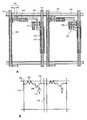
도 2는 종래의 발광장치의 일 예를 나타내는 도면.2 is a view showing an example of a conventional light emitting device.
도 3(A)∼도 3(D)는 발광장치의 제작공정을 나타내는 도면.3A to 3D are diagrams illustrating a manufacturing process of the light emitting device.
도 4(A)∼도 4(C)는 발광장치의 제작공정을 나타내는 도면.4A to 4C show a manufacturing process of the light emitting device.
도 5(A)∼도 5(C)는 발광장치의 제작공정을 나타내는 도면.5A to 5C are diagrams illustrating a manufacturing process of the light emitting device.
도 6(A)∼도 6(B)는 발광장치의 제작공정을 나타내는 도면.6 (A) to 6 (B) show manufacturing steps of the light emitting device.
도 7은 발광장치 제작공정을 실행하는 일 실시예를 나타내는 도면.7 is a view showing an embodiment of performing a light emitting device manufacturing process.
도 8은 발광장치 제작공정을 실행하는 일 실시예를 나타내는 도면.8 is a diagram illustrating an embodiment of executing a light emitting device manufacturing process.
도 9(A) 및 도 9(B)는 발광장치의 봉지(封止) 구조를 나타내는 도면.9A and 9B show a sealing structure of a light emitting device.
도 10(A) 및 도 10(B)는 발광장치의 화소부의 구조를 나타내는 도면.10A and 10B show the structure of a pixel portion of a light emitting device.
도 11(A)∼도 11(H)는 전기 장치의 예들을 나타내는 도면.11A to 11H show examples of the electric device.
도 12는 발광장치 제작공정을 실행하는 일 실시예를 나타내는 도면.12 is a view showing an embodiment of executing a light emitting device manufacturing process.
도 13은 발광장치 제작공정을 실행하는 일 실시예를 나타내는 도면.FIG. 13 is a view showing an embodiment of executing a manufacturing process of a light emitting device; FIG.
도 14는 AFM 측정 결과를 나타내는 도면.14 shows AFM measurement results.
도 15는 AFM 측정 결과를 나타내는 도면.15 shows AFM measurement results.
도 16은 AFM 측정 결과를 나타내는 도면.Fig. 16 shows the AFM measurement results.
도 17(A)∼도 17(F)는 실시예에 따른 발광장치의 제작공정을 나타내는 도면.17A to 17F show manufacturing steps of the light emitting device according to the embodiment;
도 18(A) 및 도 18(B)는 발광장치의 제조공정을 나타내는 도면,18 (A) and 18 (B) show a manufacturing process of the light emitting device;
도 19는 본 발명의 제작공정의 개념도.19 is a conceptual diagram of a manufacturing process of the present invention.
도 20(A)∼도 20(D)는 발광장치 제작공정을 실행하는 일 실시예를 나타내는 도면.20A to 20D are views showing one embodiment of executing a light emitting device fabrication process.
도 21(A)∼도 21(C)는 발광장치 제작공정을 실행하는 일 실시예를 나타내는 도면.21A to 21C show an embodiment of carrying out a light emitting device fabrication process.
도 22(A) 및 도 22(B)는 발광장치 제작공정을 실행하는 일 실시예를 나타내는 도면.22A and 22B show an embodiment of executing a light emitting device fabrication process.
도 23(A) 및 도 23(B)는 발광장치 제작공정을 실행하는 일 실시예를 나타내는 도면.23A and 23B show an embodiment of executing a light emitting device fabrication process.
*도면의 주요부분에 대한 부호의 설명** Description of the symbols for the main parts of the drawings *
802: 화소부804: 봉지 기판805: 밀봉제802: pixel portion 804: encapsulation substrate 805: sealing agent
807: 공간808: 배선809: FPC807: space 808: wiring 809: FPC
810: 기판811: 전류제어용 TFT812: 양극810: substrate 811: current control TFT 812: anode
813: n채널형 TFT814: p채널형 TFT815: 뱅크813: n-channel TFT 814: p-channel TFT 815: bank
816: 유기화합물층817: 음극818: 발광소자816: organic compound layer 817: cathode 818: light emitting element
본 발명은, 전계를 인가함으로써 발광이 얻어지는 유기화합물을 함유하는 막(이하, 유기화합물층이라 함)과, 양극, 및 음극으로 구성된 발광소자를 가지는 발광장치, 및 그 발광장치를 제작하는 방법에 관한 것이다. 구체적으로, 본 발명은, 종래 기술의 것보다 구동전압이 낮고 소자의 수명이 긴 발광소자를 사용한 발광장치에 관한 것이다. 또한, 본 명세서에서의 발광장치란, 발광소자를 사용한 화상 표시장치를 가리킨다. 또한, 발광장치는, 발광소자에 커넥터, 예를 들어, 이방 도전성 필름(FPC: 가요성 인쇄 회로) 또는 TAB(Tape Automated Bonding) 테이프 또는 TCP(Tape Carrier Packag)를 부착하여 된 모듈, TAB 테이프 또는 TCP의 말단에 인쇄 배선판이 제공되어 있는 모듈, 또는 발광소자에 COG(Chip on Glass) 방식으로 IC(집적회로)가 직접 실장되어 있는 모듈 모두를 포함하는 것으로 한다.BACKGROUND OF THE INVENTION Field of the Invention The present invention relates to a light emitting device having a film containing an organic compound (hereinafter, referred to as an organic compound layer) obtained by applying an electric field, an organic compound layer, an anode, and a cathode, and a method of manufacturing the light emitting device will be. Specifically, the present invention relates to a light emitting device using a light emitting element having a lower driving voltage and a longer lifespan than that of the prior art. In addition, the light emitting device in this specification refers to an image display device using a light emitting element. In addition, the light emitting device may be a module, TAB tape, or the like having a connector, for example, an anisotropic conductive film (FPC: flexible printed circuit) or a tape automated bonding (TAB) tape or a tape carrier packag (TCP) attached to the light emitting device. It shall include both a module provided with a printed wiring board at the end of the TCP, or a module in which an IC (integrated circuit) is directly mounted on a light emitting device in a chip on glass (COG) method.
발광소자는 박형, 경량, 고속 응답성 및 직류 저전압 구동을 포함하는 특성 때문에 차세대의 플랫 패널 디스플레이 소자로서 주목을 받고 있다. 또한, 자기발광형이고 시야각이 넓어 발광소자의 시인성(視認性)을 보다 양호하게 한다. 따라서, 발광소자는 전기 장치의 표시 화면에 사용되는 소자로서 유효한 것으로 고려되고, 활발하게 개발되고 있다.The light emitting device has attracted attention as a next generation flat panel display device because of its characteristics including thinness, light weight, high speed response and direct current low voltage driving. In addition, the self-luminous type and the wide viewing angle make the visibility of the light emitting device more favorable. Therefore, the light emitting element is considered to be effective as an element used for a display screen of an electric device, and is actively developed.
발광소자의 발광 메카니즘은, 유기화합물층을 사이에 끼운 전극들 사이에 전압을 인가함으로써, 음극으로부터 주입된 전자와 양극으로부터 주입된 정공이 유기화합물층의 발광 중심에서 재결합하여 분자 여기자를 형성하고, 이 분자 여기자가 기저 상태로 복귀할 때 에너지를 방출하여 발광한다고 말하고 있다. 유기화합물에서 생성되는 분자 여기자의 종류로서는 일중항 여기 상태와 삼중항 여기 상태가 가능하지만, 본 명세서에서는 어느 여기 상태가 발광에 기여하는 경우라도 모두 포함하는 것으로 한다.In the light emitting mechanism of the light emitting device, a voltage is applied between the electrodes sandwiching the organic compound layer so that electrons injected from the cathode and holes injected from the anode recombine at the emission center of the organic compound layer to form molecular excitons. The excitons are said to emit energy by emitting energy when they return to the ground state. Although the singlet excited state and the triplet excited state are possible as the kind of molecular excitons generated from the organic compound, in the present specification, any case where any of the excited states contribute to luminescence is included.
이러한 발광소자는 구동 방법의 차이에 의해 패시브 매트릭스(단순 매트릭스)형과 액티브 매트릭스형으로 분류된다. 이들 중 가장 주목을 끄는 것은 QVGA급 이상의 화소수를 가지고 고정세한 화상을 표시할 수 있는 액티브 매트릭스형 소자이다.Such light emitting devices are classified into a passive matrix (simple matrix) type and an active matrix type due to differences in driving methods. The most noticeable of these is an active matrix device capable of displaying high-definition images with a pixel count of QVGA or higher.
발광소자를 가지는 액티브 매트릭스형 발광장치는 도 2에 도시된 것과 같은 소자 구조를 가진다. 기판(201)상에 TFT(202)가 형성되고, 이 TFT(202)상에 층간절연막(203)이 형성되어 있다.An active matrix light emitting device having a light emitting element has an element structure as shown in FIG. A
그리고, 층간절연막(203)상에는, 배선(204)을 통해 TFT(202)에 전기적으로 접속되도록 양극(화소 전극)(205)이 형성되어 있다. 양극(205)에 적합한 재료는, 일 함수가 큰 투명한 전도성 재료이고, ITO(Indium Tin Oxide)막, 산화주석(SnO2)막, 산화인듐과 산화아연(ZnO)의 합금막, 반투명 금(金)막, 폴리아닐린 막 등이 제안되어 있다. 이들 중에서 ITO 막은 약 3.85 eV의 밴드 갭을 가지고 가시광 영역에서 매우 투명하기 때문에 가장 많이 사용된다.An anode (pixel electrode) 205 is formed on the
양극(205)상에는 유기화합물층(206)이 형성되어 있다. 본 명세서에서, 양극과 음극 사이에 제공된 모든 층을 유기화합물층이라 정의한다. 구체적으로는, 유기화합물층(206)은 발광층, 정공 주입층, 전자 주입층, 정공 수송층, 전자 수송층 등을 포함한다. 기본적으로, 발광소자는 양극, 발광층 및 음극이 차례로 적층된 구조를 가지지만, 이 구조 외에, 양극, 정공 주입층, 발광층 및 음극이 차례로 적층된 적층체, 또는, 양극, 정공 주입층, 발광층, 전자 수송층 및 음극이 차례로 적층된 구조를 가질 수도 있다.The
유기화합물층(206)이 형성된 후, 음극(207)이 형성되어 발광소자(209)를 완성한다. 음극은, 일 함수가 작은 금속(대표적으로는, 주기율표의 1족 또는 2족에 속하는 금속)으로 형성되는 일이 많다. 본 명세서에서는, 이러한 금속(알칼리 금속 및 알칼리토류 금속을 포함)을 알칼리 금속이라 부른다.After the
또한, 양극의 엣지(edge)를 덮어 그 위치에서 양극과 음극 사이의 단락을 방지하기 위해 유기 수지 재료로 된 뱅크(208)가 형성되어 있다.In addition, a
도 2는 하나의 화소와 그곳에 형성된 발광소자를 나타낸다. 실제로는, 화소부에는 도 2에 도시된 바와 같은 구조로 된 발광소자가 다수 제공되어 액티브 매트릭스형 발광장치를 구성한다.2 shows one pixel and a light emitting element formed thereon. In practice, the pixel portion is provided with a plurality of light emitting elements having a structure as shown in Fig. 2 to constitute an active matrix light emitting device.
상기한 종래의 발광장치 구조에서는, 층간절연막과 그 층간절연막 상에 형성된 양극(투명한 도전성 재료)이 상이한 열팽창률을 가진다. 이러한 종래의 발광장치 구조에서와 같이, 상이한 열팽창률을 가지는 재료들이 서로 접하여 있는 구조에 열 처리를 행하면, 열팽창률이 작은 재료(이 경우에는 양극) 측의 계면에 균열이 발생한다. 양극은 발광에 관여하는 정공을 유기화합물층에 주입하는 전극이다. 이 양극에 균열이 발생하면, 이 균열은 정공의 발생에 악영향을 미치고, 주입되는 정공의 수를 감소시키며, 발광소자 자체를 열화(劣化)시키는 원인이 되는 것으로 고려된다. 또한, 양극 표면의 요철이 정공의 발생과 주입에 악영향을 미친다.In the above-described conventional light emitting device structure, the interlayer insulating film and the anode (transparent conductive material) formed on the interlayer insulating film have different coefficients of thermal expansion. As in such a conventional light emitting device structure, when heat treatment is performed on a structure in which materials having different thermal expansion coefficients are in contact with each other, a crack occurs at an interface on the side of a material having a small thermal expansion coefficient (in this case, an anode). An anode is an electrode which inject | pours the hole which participates in light emission into an organic compound layer. If a crack occurs in this anode, it is considered that this crack adversely affects the generation of holes, reduces the number of holes to be injected, and causes deterioration of the light emitting element itself. In addition, irregularities on the surface of the anode adversely affect the generation and injection of holes.
또한, 유기화합물층은 산소나 수분에 의해 쉽게 열화되는 성질을 가지고 있다. 이러한 사실에도 불구하고, 폴리이미드, 폴리아미드 및 아크릴과 같은 유기 수지 재료를 사용하여 층간절연막을 형성하는 일이 많고, 이 층간절연막으로부터 방출된 산소 또는 다른 가스가 발광소자를 열화시킨다.In addition, the organic compound layer has a property of being easily degraded by oxygen or moisture. In spite of this fact, an interlaminar insulating film is often formed using organic resin materials such as polyimide, polyamide, and acryl, and oxygen or other gas emitted from the interlaminar insulating film degrades the light emitting element.
또한, 발광소자의 음극은 TFT 특성에 치명적인 타격을 줄 수 있는 Al 또는 Mg과 같은 알칼리 금속 재료로 형성된다. TFT의 활성층에 혼입된 알칼리 금속은 TFT의 전기적 특성을 변화시켜, TFT가 장기 신뢰성을 가지게 하는 것이 불가능하다.In addition, the cathode of the light emitting element is formed of an alkali metal material such as Al or Mg, which can cause a fatal blow to the TFT characteristics. Alkali metal incorporated into the active layer of the TFT changes the electrical characteristics of the TFT, making it impossible to make the TFT have long-term reliability.
TFT 특성의 손상을 피하기 위해, TFT 제조공정 처리실(청정실(clean room))을 발광소자 제조공정 처리실(청정실)로부터 분리시켜 TFT 활성층의 알칼리 금속에 의한 오염을 방지하는 것이 바람직하다. 그러나, 알칼리 금속에 의한 오염을 방지하기 위해, 처리실(청정실)들 사이에서 기판을 이동시키는 것이 제조공정에 포함되면, TFT 기판이 공기 중의 먼지나 다른 오염물에 의해 오염될 수 있고, TFT 소자가 정전(靜電) 방전에 의해 파괴될 수 있다는 또 다른 문제가 발생한다.In order to avoid damaging the TFT characteristics, it is preferable to separate the TFT manufacturing process chamber (clean room) from the light emitting element manufacturing process chamber (clean chamber) to prevent contamination by alkali metals of the TFT active layer. However, in order to prevent contamination by alkali metals, if the manufacturing process involves moving the substrate between the processing chambers (clean chambers), the TFT substrate may be contaminated by dust or other contaminants in the air, and the TFT element may be out of power. Another problem arises that it can be destroyed by (discharge) discharge.
따라서, 본 발명은, 종래의 것보다 열화가 적은 구조에 의해 상기한 문제가 없는 긴 수명의 발광소자를 가지는 고품질의 발광장치 및 그 발광장치를 제조하는 방법을 제공하는 것을 목적으로 한다.Accordingly, an object of the present invention is to provide a high quality light emitting device having a light emitting element having a long life without the above-mentioned problem by the structure of less deterioration than the conventional one, and a method of manufacturing the light emitting device.
본 발명은, 절연체 상에 형성된 TFT 상에 층간절연막을 형성하고, 그 층간절연막 상에 절연막을 형성하고, 배선을 통해 TFT에 전기적으로 접속되도록 양극을 형성하고, 양극 및 배선을 덮도록 수지 절연막을 형성되고, 이 수지 절연막을 에칭하여 뱅크를 형성하고, 가열처리 후에 양극을 와이핑(wiping)하고, 양극 및 뱅크를 덮도록 절연막을 형성하는 것을 특징으로 한다.According to the present invention, an interlayer insulating film is formed on a TFT formed on an insulator, an insulating film is formed on the interlayer insulating film, an anode is formed so as to be electrically connected to the TFT through wiring, and a resin insulating film is formed so as to cover the anode and the wiring. And forming a bank by etching the resin insulating film, wiping the anode after heat treatment, and forming an insulating film to cover the anode and the bank.
이와 같이 층간절연막과 양극 사이에 절연막을 형성함으로써, 상이한 열팽창률을 가지는 인접한 재료들에서 가열처리에 의해 야기되는 균열의 발생을 억제할 수 있다. 그리하여, 발광소자는 긴 수명을 가질 수 있다. 또한, 이 절연막은 층간절연막으로부터 방출된 가스 또는 수분이 발광소자에 도달하는 것을 방지할 수도 있다. 이 절연막은 무기 절연막일 수도 있고, 또는 플라즈마 처리를 통한 표면 개질에 의해 얻어지는 경화 막 또는 DLC(diamond-like carbon) 막일 수도 있다.By forming an insulating film between the interlayer insulating film and the anode in this manner, it is possible to suppress the occurrence of cracks caused by heat treatment in adjacent materials having different thermal expansion rates. Thus, the light emitting element can have a long lifespan. This insulating film can also prevent the gas or moisture emitted from the interlayer insulating film from reaching the light emitting element. This insulating film may be an inorganic insulating film, or may be a cured film or a diamond-like carbon (DLC) film obtained by surface modification through plasma treatment.
양극을 와이핑함으로써, 양극 표면의 요철이 평탄화될 수 있고, 양극 표면의 먼지가 제거될 수 있다.By wiping the anode, irregularities on the surface of the anode can be flattened, and dust on the surface of the anode can be removed.
또한, 양극 및 뱅크를 덮는 절연막을 형성함으로써, 유기화합물층에 주입되는 정공과 전자의 양의 균형을 맞추는 효과도 기대될 수 있다.In addition, by forming an insulating film covering the anode and the bank, the effect of balancing the amount of holes and electrons injected into the organic compound layer can also be expected.
본 발명의 다른 양태는, 뱅크를 형성하기 위한 수지 절연막을 형성하고, 기판을, 알칼리 금속 및 다른 것에 의한 오염을 피할 수 있는 처리실로 이동시키고, 수지 절연막을 에칭하여 뱅크를 형성하는 것을 특징으로 한다.Another aspect of the invention is characterized in that a resin insulating film for forming a bank is formed, the substrate is moved to a processing chamber in which contamination by alkali metals and others is avoided, and the resin insulating film is etched to form a bank. .
TFT의 반도체막을 보호하기 위한 절연막을 형성한 후, 대전방지 처리를 행한다. TFT 기판을 형성하기 위한 제1 처리실(제1 청정실)을 발광소자를 형성하기 위한 제2 처리실(제2 청정실)로부터 분리한다. 그리하여, 발광소자의 음극을 형성하는 Al 또는 Mg와 같은 알칼리 금속 재료로부터의 알칼리 금속이 TFT의 활성층에 혼입되는 위험을 줄인다. 그 결과, TFT의 전기적 특성 및 장기 신뢰성이 향상될 수 있다.After forming an insulating film for protecting the semiconductor film of the TFT, an antistatic treatment is performed. The first processing chamber (first clean room) for forming the TFT substrate is separated from the second processing chamber (second clean room) for forming the light emitting element. Thus, the risk of incorporation of an alkali metal from an alkali metal material such as Al or Mg forming the cathode of the light emitting element into the active layer of the TFT is reduced. As a result, the electrical characteristics and long-term reliability of the TFT can be improved.
대전방지막은 뱅크, 양극, 및 배선을 형성하는 수지 절연막에 악영향을 미치지 않는 재료로부터 형성되고, 수세(水洗) 또는 유사한 다른 간단한 방법으로 제거될 수 있다. 그러한 재료로서는, 대전방지 처리를 행하는데 필요한 도전성을 가지는 재료가 적합하다(예를 들어, 10-8[S/m] 이상). 일반적으로는 유기 도전성 재료가 사용되고, 예를 들어, 도전성 폴리머를 포함하는 대전방지막은 스핀 코팅법에 의해 형성되고, 도전성 저분자 재료를 포함하는 대전방지막은 증착법에 의해 형성된다. 구체적으로는, 폴리에틸렌 디옥시티오펜(PEDOT), 폴리아닐린(PAni), 글리세린 지방산 에스테르, 폴리옥시에틸렌 알킬 에테르, 폴리옥시에틸렌 알킬페닐 에테르, N,N-비스(2-히드록시에틸)알킬아민[알킬 디에탄올아민], N-2-히드록시에틸-N-2-히드록시알킬아민[히드록시알킬 모노에탄올아민], 폴리옥시에틸렌 알킬아민, 폴리옥시에틸렌 알킬아민 지방산 에스테르, 알킬 디에탄올아미드, 알킬 술포네이트, 알킬벤젠술포네이트, 알킬 포스페이트, 테트라알킬암모늄염, 트리알킬벤질암모늄염, 알킬 베타인, 알킬 이미다졸리움 베타인 등이 사용된다. 이들 재료는 물 또는 유기 용매에 의해 쉽게 제거될 수 있다. 그 외에, 폴리이미드, 아크릴, 폴리아미드, 폴리이미드아미드 또는 BCB(벤조시클로부텐)과 같은 유기 절연 재료가 대전방지막으로 사용될 수 있다. 상기한 재료로부터 형성된 대전방지막은 모든 실시예에 적용될 수 있다.The antistatic film is formed from a material which does not adversely affect the bank, the anode, and the resin insulating film forming the wiring, and can be removed by water washing or other similar simple methods. As such a material, a material having conductivity necessary for performing an antistatic treatment is suitable (for example, 10−8 [S / m] or more). Generally, an organic conductive material is used, for example, an antistatic film containing a conductive polymer is formed by a spin coating method, and an antistatic film containing a conductive low molecular material is formed by a vapor deposition method. Specifically, polyethylene dioxythiophene (PEDOT), polyaniline (PAni), glycerin fatty acid ester, polyoxyethylene alkyl ether, polyoxyethylene alkylphenyl ether, N, N-bis (2-hydroxyethyl) alkylamine [alkyl Diethanolamine], N-2-hydroxyethyl-N-2-hydroxyalkylamine [hydroxyalkyl monoethanolamine], polyoxyethylene alkylamine, polyoxyethylene alkylamine fatty acid ester, alkyl diethanolamide, alkyl Sulfonates, alkylbenzenesulfonates, alkyl phosphates, tetraalkylammonium salts, trialkylbenzylammonium salts, alkyl betaines, alkyl imidazolium betaines and the like. These materials can be easily removed by water or organic solvents. In addition, an organic insulating material such as polyimide, acrylic, polyamide, polyimideamide or BCB (benzocyclobutene) can be used as the antistatic film. The antistatic film formed from the above materials can be applied to all embodiments.
본 발명의 또 다른 양태는, 뱅크를 형성하고, 양극에 가열처리를 행하여 결정화한 후, 뱅크 표면에 플라즈마 처리를 행하는 공정을 포함하는 것을 특징으로 한다.Another aspect of the invention is characterized by including a step of forming a bank, performing a heat treatment on the anode to crystallize, and then performing a plasma treatment on the surface of the bank.
플라즈마 처리에 의한 표면 개질을 통해 뱅크의 표면에 경화 막이 형성된다. 이것은, 뱅크가 수분을 방출하여 발광소자를 열화시키는 것을 방지한다.A cured film is formed on the surface of the bank through surface modification by plasma treatment. This prevents the bank from releasing moisture to deteriorate the light emitting element.
[실시형태]Embodiment
기판(100)상에 TFT(101)를 형성한다. 여기서 나타낸 TFT는 발광소자로 흐르는 전류를 제어하기 위한 TFT이고, 본 명세서에서는 전류제어용 TFT(101)라 부른다.(도 1(A))The
그 다음, 전류제어용 TFT(101)상에, 평탄화를 위해 층간절연막(102)을 형성한다. 층간절연막(102)은 폴리이미드, 아크릴, 폴리아미드, 폴리이미드아미드, 에폭시 수지 또는 BCB(벤조시클로부텐)와 같은 유기 수지 재료로부터 약 1.0∼2.0 ㎛의 평균 두께를 가지도록 형성된다. 층간절연막(102)을 형성함으로써, 양호하게 평탄화를 행할 수 있다. 또한, 층간절연막은, 유기 수지 재료가 일반적으로 낮은 유전율을 가지므로 기생용량을 감소시킬 수 있다.Then, an
그 다음, 층간절연막(102)으로부터 방출되는 가스가 발광소자에 악영향을 미치지 않도록 하기 위해, 층간절연막(102)상에 제1 절연막(103)을 형성한다. 이 제1 절연막은 무기 절연막, 대표적으로는, 산화규소막, 산화질화규소막, 질화규소막 또는 상기 막들을 조합시킨 적층막이다. 제1 절연막은, 플라즈마 CVD법으로, 반응 압력을 20∼200 Pa, 기판 온도를 300∼400℃, 고주파(13.56 ㎑) 전력 밀도를 0.1∼1.0 W/㎠으로 하여 방전시켜 형성된다. 또는, 층간절연막의 표면에 행해지는 플라즈마 처리에 의해, 수소, 질소, 할로겐화 탄소, 불화수소 및 희가스로 이루어진 군에서 선택된 1종 또는 다수 종류의 가스 원소를 함유하는 경화 막이 형성된다.Next, in order to prevent the gas emitted from the
그 후, 소망의 패턴을 가지는 레지스트 마스크를 형성하고, 전류제어용 TFT(101)의 드레인 영역에 이르는 콘택트 홀을 형성하여 배선(104)을 형성한다. 이 배선은 도전성 금속막으로서 Al막 또는 Ti막 또는 Al과 Ti의 합금막으로 형성된다. 이 재료를 스퍼터링법 또는 진공증착법에 의해 성막하고, 얻어진 막을 소망의 형상으로 패터닝한다.Thereafter, a resist mask having a desired pattern is formed, and contact holes leading to the drain region of the
그 다음, 발광소자의 양극으로 작용하는 투명 도전막(105)을 형성한다. 투명 도전막(105)은 대표적으로는 산화인듐주석(ITO) 또는 2∼20%의 산화아연이 혼합된 산화인듐으로 형성된다.Then, a transparent
투명 도전막(105)을 에칭하여 양극(106)을 형성한다. 그 후, 뱅크(107)를 형성하고, 230∼350℃에서 가열처리한다. 본 명세서에서는, 양극의 위쪽에 개구부를 가지고 양극의 엣지를 덮는 절연막을 "뱅크"라 칭한다.(도 1(B) 및 도 1(C))The transparent
그 다음, 양극(106)의 표면을 평탄화하고 그 표면으로부터 먼지를 제거하기 위해, 세정액과 함께 PVA(폴리비닐 알코올)계 다공질 재료를 사용하여 양극(106)의 표면을 닦는다. 본 명세서에서, 양극(106)의 표면을 평탄화하고 그 표면으로부터 먼지를 제거하기 위해, PVA(폴리비닐 알코올)계 다공질 재료를 사용하여 양극(106)의 표면을 닦는 것을 와이핑이라고 표현한다.Then, in order to planarize the surface of the
양극 표면을 와이핑한 후, 제2 절연막(110)을 형성하고, 이 제2 절연막(110)상에 유기화합물층(111)과 음극(112)을 차례로 형성한다. 제2 절연막(110)은 1∼5 ㎚의 두께로 스핀 코팅법에 의해 형성된 폴리이미드, 폴리아미드, 아크릴 또는 다른 유기 수지 절연막이다.After wiping the surface of the anode, a second
유기화합물층(111)은, 발광층 외에, 정공 주입층, 정공 수송층, 정공 차단층, 전자 수송층, 전자 주입층, 버퍼층 등을 조합하여 가지는 적층체이다. 유기화합물층(111)의 두께는 10∼400 ㎚인 것이 바람직하다.The
유기화합물층(111)을 형성한 후, 음극(112)을 증착법에 의해 형성한다. 음극(112)의 재료는 MgAg 또는 Al-Li 합금(알루미늄과 리튬의 합금)이다. 또는, 음극은 주기율표의 1족 또는 2족에 속하는 원소와 알루미늄의 공(共)증착에 의해 형성된 막일 수도 있다. 음극(112)의 두께는 약 80∼200 ㎚인 것이 바람직하다.After the
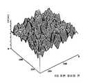
와이핑 처리 후, 투명 도전막의 표면 상태를 원자력 현미경(AFM)을 이용하여 관찰하고, 그 결과를 도 14∼도 16에 나타낸다.After the wiping treatment, the surface state of the transparent conductive film was observed using an atomic force microscope (AFM), and the results are shown in FIGS. 14 to 16.
본 실시형태에서의 표면 관찰은 측정 표면으로서, 유리 기판 상에 110 ㎚의 두께로 형성되고 250℃에서의 가열처리에 의해 결정화된 ITO막을 사용한다.Surface observation in this embodiment uses the ITO film | membrane formed at 110 nm in thickness on the glass substrate, and crystallized by heat processing at 250 degreeC as a measurement surface.
도 14 및 도 15는 AFM에 의해 관찰된 기판 표면의 요철 형상을 나타낸다. 도 14에 나타낸 것은 와이핑 처리 전의 측정 표면을 관찰한 결과이고, 도 15는 와이핑 처리 후의 측정 표면을 관찰한 결과를 나타낸다.14 and 15 show the uneven shape of the substrate surface observed by AFM. 14 shows the results of observing the measurement surface before the wiping treatment, and FIG. 15 shows the results of observing the measurement surface after the wiping treatment.
도 16은 와이핑용 PVA계 다공질 재료로서 Bellclean(Ozu 사의 제품)을 사용한 와이핑 처리 전후의 평균 표면 조도(粗度)(Ra)을 나타낸다. 여기서의 평균 표면 조도는 JIS B0601에 의해 정의된 중심선 평균 조도를 관찰되는 면에 대해 적용할 수 있도록 3차원적으로 확장한 것이다. 이 결과로부터, 와이핑 후에 측정 표면의 평균 표면 조도가 감소되고, 평탄성이 증가한 것을 알 수 있다.Fig. 16 shows average surface roughness Ra before and after wiping treatment using Bellclean (manufactured by Ozu) as a PVA-based porous material for wiping. The average surface roughness here is extended three-dimensionally so that the centerline average roughness defined by JIS B0601 can be applied to the observed surface. From this result, it can be seen that the average surface roughness of the measurement surface is reduced after wiping, and the flatness is increased.
[실시예 1]Example 1
본 실시예에서는, 본 발명을 이용하여 제조된 발광소자에 대하여 설명한다. 여기서는, 화소부 TFT와 구동회로 TFT(n채널형 TFT 및 p채널형 TFT)를 동일 기판 상에 동시에 제조하는 방법의 일 예를 도 3∼도 6을 참조하여 설명한다. 화소부는 본 발명의 발광소자를 가진다. 구동회로는 화소부의 주변에 제공되어 있다.In this embodiment, a light emitting device manufactured using the present invention will be described. Here, an example of a method of simultaneously manufacturing the pixel portion TFT and the driving circuit TFT (n-channel TFT and p-channel TFT) on the same substrate will be described with reference to FIGS. The pixel portion has the light emitting element of the present invention. The driving circuit is provided around the pixel portion.
먼저, 유리 기판(900)을 준비한다. 본 실시예에서는, 기판(900)으로서, 코닝 #7059 유리 또는 #1737 유리로 대표되는 바륨 붕규산 유리 또는 알루미노 붕규산 유리를 사용할 수 있다. 기판(900)은 투광성을 가지는 기판이면 어느 것이나 사용 가능하고, 석영 기판도 사용할 수 있다. 본 실시예의 처리 온도에 견디는 내열성을 가지는 플라스틱 기판도 사용될 수 있다.First, the
그 다음, 도 3(A)에 도시한 바와 같이, 기판(900)상에, 산화규소막, 질화규소막 또는 산화질화규소막과 같은 절연막으로 된 하지(下地) 절연막(901)을 형성한다. 본 실시예에서는, 하지 절연막(901)이 2층 구조를 가지지만, 상기한 절연막의 단층막 또는 2층 이상 적층한 막을 하지 절연막으로서 사용할 수 있다. 하지 절연막의 제1 층은 플라즈마 CVD법에 의해 반응 가스로서 SiH4, NH3, 및 N2O를 사용하여 10∼200 ㎚(바람직하게는, 50∼100 ㎚)의 두께로 형성한 산화질화규소막(901a)이다. 본 실시예에서 형성된 산화질화규소막(901a)(조성비: Si=32%, O=27%, N=24%, H=17%)의 두께는 50 ㎚이다. 하지 절연막(901)의 제2 층은 플라즈마 CVD법에 의해 반응 가스로서 SiH4 및 N2O를 사용하여 50∼200 ㎚(바람직하게는, 100∼150 ㎚)의 두께로 형성한 산화질화규소막(901b)이다. 본 실시예에서 형성된 산화질화규소막(901b)(조성비: Si=32%, O=59%, N=7%, H=2%)의 두께는 100 ㎚이다.Then, as shown in Fig. 3A, a
그 다음, 하지 절연막(901)상에 반도체층(902∼905)을 형성한다. 반도체층(902∼905)은 공지의 방법(스퍼터링법, LPCVD법, 플라즈마 CVD법 등)으로 비정질 구조를 가진 반도체막을 형성한 후 이 막에 공지의 결정화 처리(예를 들어, 레이저 결정화, 열 결정화 또는 니켈 또는 다른 촉매를 사용한 열 결정화)를 행하여 얻어진 결정성 반도체막을 소망의 형상으로 패터닝하여 형성된다. 반도체층(902∼905) 각각은 25∼80 ㎚(바람직하게는, 30∼60 ㎚)의 두께를 가진다. 결정성 반도체막의 재료는 한정되지 않고, 규소 또는 규소 게르마늄(SiXGe1-X(x = 0.0001∼0.02)) 합금이 바람직하다. 본 실시예에서는, 두께 55 ㎚의 비정질 규소막을 플라즈마 CVD법에 의해 형성한 다음, 그 비정질 규소막의 상면에 니켈을 함유하는 용액을 보유시킨다. 그 다음, 비정질 규소막을 탈수소화(500℃에서 1시간)한 다음, 열 결정화(550℃에서 4시간)한 후, 결정성의 향상을 위한 레이저 어닐 처리를 행하여, 결정성 반도체막을 얻는다. 이 결정성 규소막에 포토리소그래피를 이용한 패터닝 처리를 행하여, 반도체층(902∼905)을 형성한다.Next, the semiconductor layers 902 to 905 are formed on the
반도체층(902∼905)을 형성한 후, TFT의 스레시홀드를 제어하기 위해 미량의 불순물 원소(붕소 또는 인)를 반도체층(902∼905)에 도핑할 수도 있다.After the semiconductor layers 902 to 905 are formed, a small amount of impurity elements (boron or phosphorus) may be doped into the semiconductor layers 902 to 905 to control the threshold of the TFT.
레이저 결정화법으로 결정성 반도체막을 형성하는 경우에는, 펄스 발진형 또는 연속 발광형 엑시머 레이저, YAG 레이저 또는 YVO4 레이저를 사용할 수 있다. 이들 레이저 중에서 선택된 어느 하나에 의해 방출되는 레이저광은 반도체막을 조사하기 전에 광학계에 의해 선형 빔으로 집광되는 것이 바람직하다. 결정화의 조건은 실시자에 의해 적절히 설정될 수 있으나, 몇가지 바람직한 조건이 있다. 엑시머 레이저를 사용하는 경우, 바람직한 조건은, 펄스 발진 주파수를 300 ㎐로 하고, 레이저 에너지 밀도를 100∼400 mJ/㎠(대표적으로는, 200∼300 mJ/㎠)으로 하는 것이다. YAG 레이저를 사용하는 경우, 바람직한 조건은, 그의 제2 고조파를 사용하고, 펄스 발진 주파수를 30∼300 ㎑로 하고, 레이저 에너지 밀도를 300∼600 mJ/㎠(대표적으로는, 350∼500 mJ/㎠)으로 하는 것이다. 레이저광을 100∼1000 ㎛, 예를 들어, 400 ㎛의 폭을 가지는 선형 빔으로 집광하여 기판의 전면(全面)을 조사한다. 이 조사에서의 선형 레이저광의 중첩비(오버랩비)는 50∼90%로 한다.When the crystalline semiconductor film is formed by the laser crystallization method, a pulse oscillation type or continuous emission type excimer laser, a YAG laser or a YVO4 laser can be used. It is preferable that the laser light emitted by any one of these lasers is focused by a linear beam by the optical system before irradiating the semiconductor film. The conditions for crystallization may be appropriately set by the practitioner, but there are some preferred conditions. When using an excimer laser, preferable conditions are a pulse oscillation frequency 300 Hz and laser energy density 100-400 mJ / cm <2> (typically 200-300 mJ / cm <2>). When using a YAG laser, preferable conditions are using the 2nd harmonic, its pulse oscillation frequency is 30-300 Hz, and a laser energy density of 300-600 mJ / cm <2> (typically 350-500 mJ / Cm 2). The laser beam is focused with a linear beam having a width of 100 to 1000 mu m, for example 400 mu m, to irradiate the entire surface of the substrate. The overlap ratio (overlap ratio) of the linear laser light in this irradiation is 50 to 90%.
그 다음, 반도체층(902∼905)을 덮도록 게이트 절연막(906)을 형성한다. 게이트 절연막(906)은 규소를 함유하는 절연막으로부터 플라즈마 CVD법이나 스퍼터링법에 의해 40∼150 ㎚의 두께로 형성된다. 본 실시예에서는, 플라즈마 CVD법에 의해 110 ㎚의 두께로 형성된 산화질화규소막(조성비: Si=32%m O=59%, N=7%, H=2%)을 사용한다. 물론, 게이트 절연막은 산화질화규소막에 한정되지 않고, 규소를 함유하는 다른 절연막의 단층 또는 적층 구조일 수도 있다.Next, a
게이트 절연막에 산화규소막을 사용하는 경우에는, 플라즈마 CVD법에 의해 TEOS(tetraethyl orthosilicate)와 O2를 혼합하고, 반응 압력을 40 Pa로 하고, 기판 온도를 300∼400℃로 하고, 고주파(13.56 ㎑) 전력 밀도를 0.5∼0.8 W/㎠으로 하여 방전시켜 막을 형성한다. 이렇게 형성된 산화규소막에 대하여 그 후 400∼500℃의 열 어닐을 항하면, 게이트 절연막으로서 우수한 특성이 제공될 수 있다.When a silicon oxide film is used for the gate insulating film, TEOS (tetraethyl orthosilicate) and O2 are mixed by the plasma CVD method, the reaction pressure is 40 Pa, the substrate temperature is 300 to 400 ° C, and the high frequency (13.56 ㎑) ) Discharge at a power density of 0.5 to 0.8 W / cm 2 to form a film. If the silicon oxide film thus formed is then subjected to thermal annealing at 400 to 500 占 폚, excellent characteristics can be provided as the gate insulating film.
그리고, 게이트 절연막(906)상에, 게이트 전극을 형성하기 위한 내열성 도전층(907)을 200∼400 ㎚(바람직하게는, 250∼350 ㎚)의 두께로 형성한다. 내열성 도전층(907)은 단층이거나, 필요에 따라 2층, 3층 또는 그 이상의 층으로 된 적층 구조일 수도 있다. 내열성 도전층은 Ta, Ti 및 W으로 이루어진 군에서 선택된 원소를 함유하는 막일 수 있다. 또는, 내열성 도전층은 상기한 원소 및 다른 원소들 중의 하나를 함유하는 합금막이거나 또는 상기한 원소들을 조합한 합금막일 수 있다. 내열성 도전층을 형성하기 위해서는 스퍼터링법이나 CVD법을 사용한다. 내열성 도전층의 저저항화를 모도하기 위해서는, 이 층에 함유되는 불순물의 농도를 낮추는 것이 바람직하고, 특히 산소 농도를 30 ppm 이하로 하는 것이 바람직하다. 본 실시예에서는, W 막을 300 ㎚의 두께로 형성한다. W 막은 W을 타겟으로 하여 스퍼터링법에 의해 형성되거나, 또는 6불화 텅스텐(WF6)을 사용한 열 CVD법에 의해 형성된다. 어느 경우라도, 게이트 전극으로서 W 막을 사용하기 위해서는, W 막을 저저항화하여야 한다. W 막의 바람직한 저항률은 20 ㏁㎝ 이하이다. W 막의 저항률은 결정립을 크게 함으로써 저하될 수 있으나, W 막 중에 산소와 같은 불순물 원소가 다량 존재하면, 결정화가 저해되어 고저항화한다. 따라서, W 막을 스퍼터링법에 의해 형성하는 경우, 순도 99.9∼99.9999%의 W 타겟을 사용하고, 성막 시에 기상(氣相) 중의 불순물이 W 막에 혼입되지 않도록 많은 주의를 하여야 한다. 그 결과, W 막은 9∼20 μΩ㎝의 저항률을 가질 수 있다.On the
스퍼터링법을 사용하여 내열성 도전층(907)을 위한 Ta 막을 형성할 수도 있다. Ta 막은 스퍼터링 가스로서 Ar을 사용하여 형성된다. 적정량의 Xe 또는 Kr을 스퍼터링 가스에 첨가하면, 얻어진 Ta 막의 내부 응력이 완화되어 Ta 막의 벗겨짐을 방지할 수 있다. α상의 Ta 막의 저항률은 약 20 μΩ㎝이고, 게이트 전극으로 사용 가능하다. 한편, β상의 Ta 막의 저항률은 약 180 μΩ㎝이고, 게이트 전극으로서 적합하지 않다. Ta 막의 베이스로서 α상의 것에 가까운 결정 구조를 가지는 TaN 막을 형성함으로써 α상의 Ta 막을 쉽게 얻을 수 있다. 도면에는 도시되지 않았으나, 내열성 도전층(907) 아래에 약 2∼20 ㎚의 두께로 인(P)이 도핑된 규소막을 형성하는 것이 효과적이다. 이것은 그 위에 형성되는 도전막의 밀착성을 향상시키고, 산화를 방지한다. 동시에, 이 규소막은 내열성 도전층(907, 908)에 함유된 미량의 알칼리 금속원소가 제1 형상의 게이트 절연막(906)으로 확산하는 것을 방지한다. 어떤 재료를 사용하든, 내열성 도전층(907)에 바람직한 저항률 범위는 10∼50 μΩ㎝이다.The Ta film for the heat resistant
본 실시예에서는, 제1 도전막(907)에 TaN 막을 사용하고, 제2 도전막(908)에 W 막을 사용한다.(도 3(A))In this embodiment, a TaN film is used for the first
그 다음, 포토리소그래피법을 사용하여 레지스트 마스크(909)를 형성한다. 그 다음, 제1 에칭 처리를 행한다. 제1 에칭 처리는 제1 에칭 조건 및 제2 에칭 조건 하에 행한다.Then, the resist
본 실시예에서는, ICP 에칭 장치를 사용하고, 에칭 가스로서 Cl2, CF4 및 O2를 사용하고, 그의 가스 유량비를 25/25/10으로 하고, 1 Pa의 압력에서 3.2 W/㎠의 RF(13.56 ㎒) 전력을 공급하여 플라즈마를 발생시킨다. 기판측(시료 스테이지)에도 224 mW/㎠의 RF(13.56 ㎒) 전력을 가하여, 실질적으로 부(負)의 셀프바이어스 전압을 인가한다. 제1 에칭 조건에 의해 W 막을 에칭한다. 그 다음, 레지스트 마스크를 제거하지 않고 제1 에칭 조건을 제2 에칭 조건으로 바꾼다. 제2 에칭 조건에서는, 에칭 가스로서 CF4 및 Cl2를 사용하고, 그의 가스 유량비를 30/30 SCCM으로 하고, 1 Pa의 압력에서 RF(13.56 ㎒) 전력을 공급하여 플라즈마를 발생시킨다. 기판측(시료 스테이지)에도 20 W의 RF(13.56 ㎒) 전력을 가하여, 실질적으로 부의 셀프바이어스 전압을 인가한다.In this embodiment, an ICP etching apparatus is used, Cl2 , CF4, and O2 are used as etching gases, the gas flow rate ratio is 25/25/10, and RF of 3.2 W / cm 2 at a pressure of 1 Pa. (13.56 MHz) Supply power to generate plasma. RF (13.56 MHz) power of 224 mW / cm 2 is also applied to the substrate side (sample stage) to apply a negative self-bias voltage substantially. The W film is etched by the first etching conditions. Then, the first etching condition is changed to the second etching condition without removing the resist mask. Under the second etching conditions, CF4 and Cl2 are used as etching gases, the gas flow rate ratio is 30/30 SCCM, and RF (13.56 MHz) power is supplied at a pressure of 1 Pa to generate plasma. RF (13.56 MHz) power of 20 W is also applied to the substrate side (sample stage) to apply a negative self bias voltage substantially.
제1 에칭 처리에 의해, 제1 테이퍼 형상을 가지는 도전층(910∼913)이 형성된다. 도전층(910∼913)의 테이퍼부의 각도는 15∼30°로 한다. 어떠한 잔사(殘渣)도 남기지 않고 막을 에칭하기 위해서는, 에칭 시간을 약 10∼20%만큼 연장시켜 오버에칭을 행한다. W 막에 대한 산화질화규소막(게이트 절연막(906))의 선택비는 2∼4(대표적으로는, 3)이므로, 오버에칭 처리에 의해 산화질화규소막의 노출된 표면이 20∼50 ㎚만큼 에칭된다.(도 3(B))By the first etching treatment,
그 다음, 제1 도핑 처리를 행하여, 일 도전형의 불순물 원소를 반도체층에 도핑한다. 이 도핑 공정에서는 레지스트 마스크(909)를 제거하지 않고 n형 도전성을 부여하는 불순물 원소를 첨가한다. 제1 테이퍼 형상의 도전층(910∼913)을 마스크로 사용하여 반도체층(902∼905)의 일부에 불순물 원소를 자기정합적으로 첨가하여 제1 n형 불순물 영역(914∼917)을 형성한다. n형 도전성을 부여하는 불순물 원소로서는, 주기율표의 15족 원소, 전형적으로는, 인(P) 또는 비소(As)를 사용한다. 본 실시예에서는 인을 사용하고 이온 도핑법을 사용한다. 제1 n형 불순물 영역(914∼917)에서 n형 도전성을 부여하는 불순물 원소의 농도는 1×10²⁰∼1×10²¹ 원자/㎤이다.(도 3(B))Next, a first doping treatment is performed to dope the semiconductor layer with an impurity element of one conductivity type. In this doping step, an impurity element for imparting n-type conductivity is added without removing the resist
그 다음, 레지스트 마스크를 제거하지 않고 제2 에칭 처리를 행한다. 제2 에칭 처리는 제3 에칭 조건과 제4 에칭 조건 하에 행한다. 제2 에칭 처리에서는, 제1 에칭 처리와 마찬가지로, ICP 에칭 장치를 사용하고, 에칭 가스로서 CF4 및 Cl2를 사용하고, 그의 가스 유량비를 30/30 SCCM으로 하고, 1 Pa의 압력에서 RF(13.56 ㎒) 전력을 공급하여 플라즈마를 발생시킨다. 기판측(시료 스테이지)에도 20 W의 RF(13.56 ㎒) 전력을 가하여, 실질적으로 부의 셀프바이어스 전압을 인가한다. 제3 에칭 조건에서는, W 막 및 TaN 막이 같은 정도로 에칭된 도전막(918∼921)이 형성된다.(도 3(C))Next, a second etching process is performed without removing the resist mask. The second etching treatment is performed under the third etching condition and the fourth etching condition. In the second etching treatment, similarly to the first etching treatment, an ICP etching apparatus is used, CF4 and Cl2 are used as etching gases, and the gas flow rate ratio is 30/30 SCCM, and the RF ( 13.56 MHz) to supply power to generate a plasma. RF (13.56 MHz) power of 20 W is also applied to the substrate side (sample stage) to apply a negative self bias voltage substantially. Under the third etching conditions, the
그 후, 레지스트 마스크를 그 대로 두고 에칭 조건을 제4 에칭 조건으로 바꾼다. 제4 에칭 조건에서는, 에칭 가스로서 CF4, Cl2 및 O2의 혼합 가스를 사용하고, 1 Pa의 압력에서 RF(13.56 ㎒) 전력을 공급하여 플라즈마를 발생시킨다. 기판측(시료 스테이지)에도 20 W의 RF(13.56 ㎒) 전력을 가하여, 실질적으로 부의 셀프바이어스 전압을 인가한다. 제4 에칭 조건에서 W 막이 에칭되어 제2 형상의 도전막(922∼925)을 형성한다.(도 3(D))Thereafter, the resist mask is left as it is and the etching conditions are changed to the fourth etching conditions. Under the fourth etching condition, a mixed gas of CF4 , Cl2 and O2 is used as the etching gas, and RF (13.56 MHz) power is supplied at a pressure of 1 Pa to generate plasma. RF (13.56 MHz) power of 20 W is also applied to the substrate side (sample stage) to apply a negative self bias voltage substantially. The W film is etched under the fourth etching conditions to form the second shape
그 다음, 제2 도핑 처리를 행한다(여기서, 제2 형상의 제1 도전막(922a∼925a)을 통과하여 반도체층에 n형 불순물 원소를 첨가한다). 그 결과, 제1 n형 불순물 영역(914∼917)에 접하는 채널 형성 영역 측에 각각 제2 n형 불순물 영역(926∼929)이 형성된다. 각각의 제2 n형 불순물 영역에서의 불순물 농도는 1×10¹⁶∼1×10¹⁹ 원자/㎤으로 한다. 제2 도핑 공정에서는, 제1 층의 제2 형상의 도전막(922a∼925a)의 테이퍼부를 통과하여 반도체층에 n형 불순물 원소가 첨가된다. 본 명세서에서는, 제1 층의 제2 형상의 도전막(922a∼925a)과 겹치는 제2 n형 불순물 영역의 부분을 Lov('ov'는 'overlap'을 나타냄) 영역이라 부르고, 제1 층의 제2 형상의 도전막(922a∼925a)과 겹치지 않는 제2 n형 불순물 영역의 부분을 Loff('off'는 'offset'을 나타냄) 영역이라 부른다.(도 4(A))Next, a second doping treatment is performed (here, n-type impurity element is added to the semiconductor layer through the first
그 다음, 도 4(B)에 도시한 바와 같이, p채널형 TFT의 활성층으로 작용하는 반도체층(902, 905)에 일 도전형과 반대의 도전형의 불순물 영역(932(932a, 932b), 933(933a, 933b))을 형성한다. 불순물 영역(932, 933)도 제2 도전층(922, 925)을 마스크로 하여 자기정합적으로 p형 도전성을 부여하는 불순물 원소를 반도체층에 첨가함으로써 형성된다. 이 도핑 전에, n채널형 TFT의 활성층으로 작용하는 반도체층(903, 904)의 전면을 덮도록 레지스트 마스크(930, 931)를 형성한다. 여기서 형성되는 p형 불순물 영역(932, 933)은 디보란(B2H6)을 사용한 이온 도핑법에 의해 형성한다. p형 불순물 영역(932, 933)들 각각에서 p형 도전성을 부여하는 불순물의 농도는 2×10²⁰∼2×10²¹ 원자/㎤으로 한다.Then, as shown in Fig. 4B, the impurity regions 932 (932a and 932b) opposite to the one conductivity type are formed in the semiconductor layers 902 and 905 serving as the active layers of the p-channel TFT. 933 (933a, 933b). Impurity regions 932 and 933 are also formed by adding an impurity element that imparts p-type conductivity to the semiconductor layer self-aligning with second
상세하게는, p형 불순물 영역(932, 933)은 n형 도전성을 부여하는 불순물 원소를 함유하고 있지만, n형 도전성을 부여하는 불순물 원소의 농도보다 1.5∼3배 높은 농도로 p형 도전성을 부여하는 불순물 원소를 첨가함으로써 p형 불순물 영역(932, 933)이 p채널형 TFT의 소스 영역 및 드레인 영역으로 기능하는데 아무런 문제가 없다.Specifically, the p-type impurity regions 932 and 933 contain impurity elements that impart n-type conductivity, but impart p-type conductivity to a concentration 1.5 to 3 times higher than the concentration of impurity elements that impart n-type conductivity. By adding an impurity element, p-type impurity regions 932 and 933 have no problem in functioning as a source region and a drain region of the p-channel TFT.
그 후, 도 4(C)에 도시된 바와 같이, 제2 형상의 도전층(922∼925) 및 게이트 절연막(906)상에 제1 층간절연막(934)을 형성한다. 제1 층간절연막(934)은 산화규소막, 산화질화규소막, 질화규소막이거나 또는 상기 막들을 조합한 적층막이다. 어느 경우든지, 제1 층간절연막(934)은 무기 절연 재료로 형성된다. 제1 층간절연막(934)의 두께는 100∼200 ㎚로 한다. 제1 층간절연막(934)에 산화규소막을 사용하는 경우, 플라즈마 CVD법에 의해 TEOS 및 O2를 혼합하고, 반응 압력을 40 Pa로 하고, 기판 온도를 300∼400℃로 하고, RF(13.56 ㎒) 전력 밀도를 0.5∼0.8 W/㎠으로 하여 방전시킴으로써 막을 형성한다. 제1 층간절연막(934)에 산화질화규소막을 사용하는 경우에는, 플라즈마 CVD법에 의해 SiH4, N2O 및 NH3 또는 SiH4 및 N2O로부터 막을 형성할 수 있다. 이 경우의 성막 조건은 반응 압력을 20∼200 Pa로 하고, 기판 온도를 300∼400℃로 하고, 고주파(60 ㎒) 전력 밀도를 0.1∼1.0 W/㎠로 한다. 제1 층간절연막(934)은 SiH4, N2O 및 H2로부터 형성된 산화질화수소화규소막일 수도 있다. 제1 층간절연막으로서의 질화규소막도 마찬가지로 SiH4 및 NH3로부터 플라즈마 CVD법에 의해 형성될 수 있다.Thereafter, as shown in FIG. 4C, a first
그 다음, 상이한 농도로 반도체층에 첨가된 n형 또는 p형 도전성을 부여하는 불순물 원소를 활성화하는 공정을 행한다. 이 활성화 공정은 어닐 노를 사용한 열 어닐법에 의해 행한다. 그 외에, 레이저 어닐법이나 급속 열 어닐(RTA)법을 채용할 수도 있다. 열 어닐법에서는 산소 농도가 1 ppm 이하(바람직하게는, 0.1 ppm 이하)인 질소 분위기에서 400∼700℃, 대표적으로는, 500∼600℃의 온도로 행한다. 본 실시예에서는 550℃로 4시간 가열처리를 행한다. 기판(900)으로서 내열성이 낮은 플라스틱 기판을 사용하는 경우에는, 레이저 어닐법이 바람직하다.Next, a step of activating an impurity element imparting n-type or p-type conductivity added to the semiconductor layer at different concentrations is performed. This activation process is performed by the thermal annealing method using an anneal furnace. In addition, the laser annealing method or the rapid thermal annealing (RTA) method may be employed. In the thermal annealing method, it is performed at 400-700 degreeC, typically 500-600 degreeC in nitrogen atmosphere whose oxygen concentration is 1 ppm or less (preferably 0.1 ppm or less). In this embodiment, heat treatment is performed at 550 ° C. for 4 hours. When using the plastic substrate with low heat resistance as the board |
이 가열처리 공정에서, 반도체층을 결정화하는 공정에서 사용된 촉매원소(니켈)가, 게터링 작용을 가지는 주기율표의 15족 원소(본 실시예에서는 인이 사용됨)를 고농도로 첨가한 제1 n형 불순물 영역으로 이동(게터링)된다. 게터링의 결과로, 채널 형성 영역에서 촉매원소의 농도가 감소된다.In this heat treatment step, the first n-type in which the catalytic element (nickel) used in the process of crystallizing the semiconductor layer has a high concentration of a group 15 element (phosphorus is used in this embodiment) of the periodic table having a gettering action. It is moved (gettered) to the impurity region. As a result of the gettering, the concentration of the catalytic element in the channel forming region is reduced.
활성화 공정에 이어서, 분위기 가스를 3∼100%의 수소를 함유하는 분위기로 바꾸고 300∼450℃에서 1∼12시간의 가열처리를 통해 반도체층을 수소화하는 공정을 행한다. 이 공정은 열적으로 여기된 수소에 의해 반도체층에 있는 1016∼1018/㎤의 댕글링 본드를 종단시키는 공정이다. 다른 유용한 수소화 방법으로는, 플라즈마 수소화(플라즈마 여기된 수소를 사용)가 있다. 어느 방법을 사용하든, 반도체층(902∼905)의 결함 밀도가 1016/㎤ 이하로 감소되는 것이 바람직하다. 이를 위해, 반도체층에 0.01∼0.1 원자%의 수소를 부여한다.Subsequent to the activation step, the atmosphere gas is changed to an atmosphere containing 3 to 100% of hydrogen, followed by a step of hydrogenating the semiconductor layer through heat treatment at 300 to 450 ° C. for 1 to 12 hours. This step is a step of terminating 1016 to 1018 / cm 3 dangling bond in the semiconductor layer by hydrogen that is thermally excited. Another useful hydrogenation method is plasma hydrogenation (using plasma excited hydrogen). In either case, it is preferable that the defect density of the semiconductor layers 902 to 905 be reduced to 1016 / cm 3 or less. For this purpose, 0.01-0.1 atomic% hydrogen is given to a semiconductor layer.
그리고, 유기 절연 재료로 된 제2 층간절연막(935)을 1.0∼2.0 ㎛의 평균 두께로 형성한다. 제2 층간절연막(935)은 폴리이미드, 아크릴, 폴리아미드, 폴리이미드아미드 또는 BCB(벤조시클로부텐)과 같은 유기 수지 재료로 형성될 수 있다. 예를 들어, 기판에 도포된 후 열중합되는 타입의 폴리이미드를 사용하는 경우, 청정 오븐에서 300℃로 소성(燒成)하여 막을 형성한다. 제2 층간절연막이 아크릴로 형성되는 경우, 2액성의 것이 사용된다. 주요 재료를 경화제와 혼합하고, 그 혼합물을 스피너를 사용하여 기판의 전면에 도포하고, 그 기판을 80℃의 열판에서 60초간 예비 가열한 후, 청정 오븐에서 250℃로 60분간 소성하여 막을 형성한다.The second
이와 같이 제2 층간절연막(935)을 유기 절연 재료로 형성함으로써, 제2 층간절연막(935)의 표면을 양호하게 평탄화할 수 있다. 또한, 유기 수지 재료는 일반적으로 유전율이 낮으므로, 기생용량을 감소시킬 수 있다. 그러나, 유기 수지 재료는 흡습성이므로 보호막으로는 적합하지 않다. 따라서, 본 실시예에서와 같이, 제2 층간절연막을 산화규소막, 산화질화규소막 또는 질화규소막으로 형성된 제1 층간절연막(934)과 조합하여 사용하면 좋다.Thus, by forming the second
유기 절연 재료로 형성된 제2 층간절연막(935)은 수분 및 가스를 방출할 수 있다. 발광소자는 수분 및 가스(산소)에 의해 쉽게 열화되는 것으로 알려져 있다. 실제로, 층간절연막에 유기 수지 절연막을 사용한 발광장치에서는, 발광장치의 동작 중에 발생하는 열 때문에 유기 수지 절연막으로부터 수분 및 산소가 방출되어 발광소자가 쉽게 열화되는 것으로 여겨진다. 따라서, 유기 절연 재료로 형성된 제2 층간절연막(935)상에 제1 절연막(936)을 형성한다.The second
제1 절연막(936)에는 산화규소막, 산화질화규소막, 질화규소막 등을 사용한다. 여기서는 제1 절연막(936)을 스퍼터링법이나 플라즈마 CVD법에 의해 형성한다. 제1 절연막(936)은 콘택트 홀을 형성한 후에 형성될 수도 있다.A silicon oxide film, a silicon oxynitride film, a silicon nitride film, or the like is used for the first insulating
그 다음, 소정의 패턴을 가진 레지스트 마스크를 형성하고, 소스 영역 또는 드레인 영역으로 작용하도록 반도체층에 형성된 불순물 영역에 도달하는 콘택트 홀을 형성한다. 콘택트 홀은 건식 에칭법에 의해 형성된다. 이 경우, 에칭 가스로서 CF4 및 O2의 혼합 가스를 사용하여, 먼저, 제1 절연막(936)을 에칭한 다음, 에칭 가스를 CF4, O2 및 He의 혼합 가스로 바꾸고, 유기 수지 재료로 형성된 제2 층간절연막(935)을 에칭한다. 그 다음, 에칭 가스를 CF4 및 O2로 바꾸고, 제1 층간절연막(934)을 에칭한다. 그 다음, 반도체층과의 선택비를 증가시키기 위해 에칭 가스를 다시 CHF3으로 바꾸고, 게이트 절연막(906)을 에칭한다. 이렇게 하여, 콘택트 홀이 얻어진다.Then, a resist mask having a predetermined pattern is formed, and contact holes reaching the impurity regions formed in the semiconductor layer to serve as source or drain regions are formed. The contact hole is formed by a dry etching method. In this case, using the mixed gas of CF4 and O2 as the etching gas, firstly, the first insulating
스퍼터링법이나 증착법에 의해 금속 도전막을 형성하고, 마스크를 사용하여 패터닝한다. 그 다음, 이 막을 에칭하여 배선(937∼943)을 형성한다. 도면에는 도시되지 않았으나, 본 실시예에서의 배선은 두께 50 ㎚의 Ti막과 두께 500 ㎚의 합금막(Al-Ti 합금막)의 적층막으로부터 형성된다.A metal conductive film is formed by sputtering or vapor deposition, and patterned using a mask. Then, this film is etched to form
그 다음, 그 위에 투명 도전막을 80∼120 ㎚의 두께로 형성한다. 그 다음, 이 막을 에칭하여 양극(944)을 형성한다(도 5(A)). 본 실시예에서 사용된 투명 도전막은 산화인듐주석(ITO)막 또는 2∼20%의 산화아연(ZnO)을 산화인듐에 혼합하여 얻어진 막이다.Thereafter, a transparent conductive film is formed thereon with a thickness of 80 to 120 nm. This film is then etched to form an anode 944 (Fig. 5 (A)). The transparent conductive film used in this embodiment is an indium tin oxide (ITO) film or a film obtained by mixing 2-20% zinc oxide (ZnO) with indium oxide.
양극(944)을 드레인 배선(943)과 접하여 겹치도록 형성하여, 전류제어용 TFT의 드레인 영역에 전기적으로 접속한다(도 5(A)). 여기서, 양극(944)을 180∼350℃로 가열처리할 수도 있다.The
그 다음, 도 5(B)에 도시된 바와 같이, 양극(944)상에 제3 층간절연막(945)을 형성한다. 여기서, 기판을 발광소자 형성을 위한 처리실(청정실)로 이동시킬 수도 있다. 공기 중의 먼지에 의한 TFT 기판의 오염 또는 파손을 피하기 위해, 대전방지 작용을 가지는 매우 얇은 막(946)(이하, 대전방지막이라 칭함)을 제3 층간절연막(945)상에 형성한다. 대전방지막(946)은 수세(水洗)에 의해 제거될 수 있는 재료로 형성된다(도 5(C)). 대전방지막을 형성하는 대신에, 기판을 대전방지용 케이스에 보관할 수도 있다. 처리실을 변경하기 전에, 상기한 공정들을 완료한 TFT 기판에 대하여 동작 시험을 행할 수도 있다.Next, as shown in FIG. 5B, a third
TFT 기판을 발광소자 형성을 위한 처리실(청정실)로 이동시킨 후, 대전방지막(946)을 수세에 의해 제거한다. 그 다음, 제3 층간절연막(945)을 에칭하여, 화소(발광소자)와 일치하는 위치에 개구부를 가지는 뱅크(947)를 형성한다. 본 실시예에서는 레지스트를 사용하여 뱅크(947)를 형성한다. 본 실시예에서, 뱅크(947)의 두께는 약 1 ㎛이고, 양극이 배선과 접하는 부분을 덮는 뱅크(947)의 영역은 테이퍼 형상으로 되어 있다(도 6(A)). TFT 기판을 발광소자 형성을 위한 처리실로 이동시킨 후 다시 기판에 대하여 동작 시험을 행할 수도 있다.After the TFT substrate is moved to a processing chamber (cleaning chamber) for forming a light emitting element, the
본 실시예에서는, 뱅크(947)로서 레지스트막을 사용하였으나, 경우에 따라서는 폴리이미드막, 폴리아미드막 아크릴막, BCB(벤조시클로부텐)막, 산화규소막 등을 사용할 수도 있다. 뱅크(947)는 절연성을 가지는 물질이면 무기물이거나 유기물 어느 것이어도 좋다. 감광성 아크릴을 사용하여 뱅크(947)를 형성하는 경우, 감광성 아크릴막을 에칭한 다음, 180∼350℃에서 가열처리를 행하는 것이 바람직하다. 또한, 비감광성 아크릴막을 사용하는 경우에는, 먼저 180∼350℃에서 가열처리를 행한 다음, 에칭하여 뱅크를 형성하는 것이 바람직하다.In this embodiment, a resist film is used as the
그 다음, 양극 표면에 와이핑 처리를 행한다. 본 실시예에서는, 양극(944)의 표면을 평탄화하고 먼지를 제거하기 위해 Bellclean(Ozu사의 제품)을 사용하여 양극(944)의 표면을 와이핑한다. 와이핑에서, 세척액으로서 순수(純水)를 사용하고, Bellclean을 감은 축의 회전수를 100∼300 rpm으로 하고, 눌러 내리는 값을 0.1∼1.0 ㎜로 한다.(도 6(A))Then, the wiping treatment is performed on the surface of the anode. In this embodiment, Bellclean (manufactured by Ozu) is used to wipe the surface of the
그 다음, TFT 기판을 진공 중에서 소성한다. 뱅크를 형성하는 수지 절연막으로부터 수분 및 가스를 방출시키기 위해, 일정 진공도, 예를 들어, 0.01 Torr 이하에서 진공 배기를 행한다. 진공 중에서의 소성은, 대전방지막을 제거한 후, 와이핑 처리 후 또는 발광소자의 형성 전에 행할 수도 있다.Then, the TFT substrate is baked in a vacuum. In order to discharge moisture and gas from the resin insulating film which forms a bank, vacuum evacuation is performed at a constant vacuum degree, for example, 0.01 Torr or less. Baking in vacuum may be performed after the antistatic film is removed, after the wiping treatment or before formation of the light emitting element.
뱅크(947)와 양극(944)을 덮도록 제2 절연막(948)을 형성한다. 제2 절연막(948)은 폴리이미드막, 폴리아미드막 또는 폴리이미드아미드막과 같은 유기 수지막이고, 스핀 코팅법, 증착법, 스퍼터링법 등에 의해 1∼5 ㎚의 두께로 형성된다. 이 절연막을 형성함으로써, 양극(944)의 표면의 균열을 피할 수 있고, 발광소자의 열화를 방지할 수 있다.The second
제2 절연막(948)상에 유기화합물층(949) 및 음극(950)을 증착법에 의해 형성한다. 본 실시예에서는, 발광소자의 음극으로서 MgAg 전극을 사용하였으나, 그 대신, 다른 공지의 재료를 사용할 수도 있다. 유기화합물층(949)은 발광층 이외에, 정공 주입층, 정공 수송층, 전자 수송층, 전자 주입층, 버퍼층 등을 조합하여 가지는 적층막이다. 본 실시예에서 사용된 유기화합물층의 구조에 대하여 이하에 상세히 설명한다.The
본 실시예에서는, 정공 주입층에 구리 프탈로시아닌을 사용하고, 정공 수송층에 α-NPD를 사용한다. 이들 층 모두는 증착법에 의해 형성된다.In this embodiment, copper phthalocyanine is used for the hole injection layer, and α-NPD is used for the hole transport layer. All of these layers are formed by vapor deposition.
그 다음, 발광층을 형성한다. 본 실시예에서는, 발광층에 상이한 재료를 사용하여 상이한 발광을 나타내는 유기화합물층을 형성한다. 본 실시예에서 형성된 유기화합물층은 3가지 타입, 즉, 적색 발광을 나타내는 것, 녹색 발광을 나타내는 것 및 청색 발광을 나타내는 것이 있다. 모든 타입의 유기화합물층이 증착법에 의해 형성된다. 따라서, 화소마다 다른 재료로 발광층을 형성하기 위해 금속 마스크를 사용할 수 있다.Then, the light emitting layer is formed. In this embodiment, different materials are used for the light emitting layer to form organic compound layers exhibiting different light emission. The organic compound layer formed in the present embodiment has three types, namely, red light emission, green light emission, and blue light emission. All types of organic compound layers are formed by vapor deposition. Therefore, a metal mask can be used to form the light emitting layer with a different material for each pixel.
적색으로 발광하는 발광층은 Alq3에 DCM을 도핑한 것을 사용하여 형성된다. 그 대신, N,N'-디살리실리덴-1,6-헥산디아미네이트)아연(Ⅱ)(Zn(salhn))에 Eu 착체인 (1,10-페난트롤린)-tris(1,3-디페닐-프로판-1,3-디오나토)유로퓸(Ⅲ) (Eu(DBM)3(Phen))을 도핑한 것을 사용할 수도 있다. 또한, 다른 공지의 재료도 사용할 수 있다.The light emitting layer which emits red light is formed using a doped DCM of Alq3 . Instead, the (1,10-phenanthroline) -tris (1,10-phenanthroline) -Eu complex in N, N'-disalicylidene-1,6-hexanediazonate) zinc (II) (Zn (salhn)) Doped with 3-diphenyl-propane-1,3-dionato) europium (III) (Eu (DBM)3 (Phen)) can also be used. In addition, other known materials can also be used.
녹색으로 발광하는 발광층은 CBP와 Ir(ppy)3를 공(共)증착법에 의해 형성될 수 있다. 이 때에는, BCP를 사용하여 정공 차단층을 형성하는 것이 바람직하다. 그 대신, 알루미늄 퀴놀리레이트 착체(Alq3)와 벤조퀴놀리놀레이트 베릴륨 착체(BeBq)를 사용할 수도 있다. 이 층은 도펀트로서 쿠마린 6. 퀴나크리돈 등을 사용하여 알루미늄 퀴놀리레이트 착체(Alq3)로부터 형성될 수도 있다. 또한, 다른 공지의 재료도 사용할 수 있다.The light emitting layer emitting green light may be formed by co-deposition of CBP and Ir (ppy)3 . At this time, it is preferable to form a hole blocking layer using BCP. Instead, aluminum quinolilate complexes (Alq3 ) and benzoquinolinolate beryllium complexes (BeBq) may be used. This layer may be formed from aluminum quinolate complex (Alq3 ) using coumarin 6. quinacridone or the like as a dopant. In addition, other known materials can also be used.
청색으로 발광하는 발광층은 디스틸일 유도체인 DPVBi, 리간드로서 아조메틴 화합물을 가지는 아연 착체인 N,N-디살리실리덴-1,6-헥산디아미네이트)아연(Ⅱ) (Zn(salhn)) 또는 페리렌이 도핑된 4,4'-bis(2,2-디페닐-비닐)-바이페닐(DPVBi)로부터 형성될 수 있다. 또한, 다른 공지의 재료도 사용할 수 있다.The light emitting layer emitting blue light is DPVBi, which is a dithylyl derivative, and N, N-disalicylidene-1,6-hexanediamate) zinc, which is a zinc complex having an azomethine compound as a ligand, (II) (Zn (salhn)). Or perylene doped from 4,4'-bis (2,2-diphenyl-vinyl) -biphenyl (DPVBi). In addition, other known materials can also be used.
그 다음, 전자 수송층을 형성한다. 전자 수송층에는, 1,3,4-옥사디아졸 유도체, 1,2,4-트리아졸유도체(예를 들어, TAZ) 등을 사용할 수 있다. 본 실시예에서는, 1,2,4-트리아졸유도체(TAZ)를 30∼60 nm의 두께로 증착법에 의해 형성한다.Next, an electron transport layer is formed. 1,3,4-oxadiazole derivatives, 1,2,4-triazole derivatives (for example, TAZ), etc. can be used for an electron carrying layer. In this embodiment, 1,2,4-triazole derivative (TAZ) is formed by the vapor deposition method in a thickness of 30 to 60 nm.
상기 공정들을 통해, 적층 구조를 가지는 유기화합물층이 완성된다. 본 실시예에서는, 유기화합물층(949)의 두께가 10∼400 ㎚(전형적으로는, 60∼150 ㎚)이고, 음극(950)의 두께는 80∼200 ㎚(전형적으로는, 100∼150 ㎚)이다.Through the above processes, an organic compound layer having a laminated structure is completed. In this embodiment, the thickness of the
유기화합물층을 형성한 후, 발광소자의 음극(950)을 증착법에 의해 형성한다. 본 실시예에서는, 발광소자의 음극을 구성하는 도전막에 MgAg를 사용하지만, Al-Li 합금막(알루미늄과 리튬의 합금막), 또는 주기율표의 1족 또는 2족에 속하는 원소와 알루미늄을 공(共)증착법에 의해 형성한 막을 사용할 수도 있다.After the organic compound layer is formed, the
그리하여, 도 6(B)에 도시된 구조를 가지는 발광장치가 완성된다. 양극(944), 유기화합물층(949) 및 음극(950)이 겹쳐 있는 부분(951)이 발광소자에 상당한다.Thus, the light emitting device having the structure shown in Fig. 6B is completed. The
p채널형 TFT(1000) 및 n채널형 TFT(1001)는 구동회로의 TFT이고, CMOS를 구성한다. 스위칭용 TFT(1002) 및 전류제어용 TFT(1003)는 화소부의 TFT이다. 구동회로의 TFT와 화소부의 TFT는 동일 기판상에 형성될 수 있다.The p-
발광소자를 사용한 발광장치의 경우, 구동회로는 약 5∼6 V(최대로 10 V)의 전압을 가지는 전원에 의해 작동될 수 있다. 따라서, 열 전자에 의한 TFT의 열화는 그다지 문제가 되지 않는다.In the case of a light emitting device using a light emitting element, the driving circuit can be operated by a power supply having a voltage of about 5 to 6 V (maximum 10 V). Therefore, deterioration of TFT by hot electrons does not become a problem very much.
[실시예 2]Example 2
본 실시예에서는, 발광장치의 제작공정의 다른 예를 도 19∼도 22을 참조하여 설명한다.In this embodiment, another example of the manufacturing process of the light emitting device will be described with reference to FIGS. 19 to 22.
실시예 1의 설명에 따라, 도 3(A)에 도시된 바와 같이 게이트 절연막(906)상에 2층의 도전막(906, 908)을 형성하는 공정까지의 공정을 완료한다.According to the description of the first embodiment, the steps up to the process of forming the two
이어서, 마스크(909a∼909d)를 사용하여 도전막(907, 908)을 에칭하여 제1 테이퍼 형상을 가지는 도전막(3901∼3904)을 형성하는 공정을 도 20(A)에서 설명한다. 이 에칭에 ICP(유도 결합형 플라즈마) 에칭 장치를 사용한다. 에칭 가스는 한정되지 않으나, CF4, Cl2및 O2를 사용하여 W 막 및 질화탄탈막을 에칭한다. CF4, Cl2 및 O2의 가스 유량비를 각각 25/25/10으로 하고, 1 Pa의 압력에서 코일형 전극에 500 W의 RF(13.56 ㎒) 전력을 인가하여 에칭한다. 기판측(시료 스테이지)에도 150 W의 RF(13.56 ㎒) 전력을 공급하여, 실질적으로 부의 셀프바이어스 전압을 인가할 수 있다. 이들 제1 에칭 조건 하에, 주로 W 막이 에칭되어 소정의 형상을 가진다.Next, the process of etching the
그 후, 에칭 가스를 CF4 및 Cl2로 바꾸고, 가스 유량비를 30/30으로 하고, 1 Pa의 압력에서 500 W의 RF(13.56 ㎒) 전력을 코일형 전극에 가하여 플라즈마를 발생시켜 30초간 에칭을 행한다. 기판측(시료 스테이지)에도 20 W의 RF(13.56 ㎒) 전력을 공급하여, 실질적으로 부의 셀프바이어스 전압을 인가할 수 있다. CF4 및 Cl2의 혼합 가스에서는, 질화탄탈막과 W 막이 거의 같은 속도로 에칭된다. 그리하여, 제1 테이퍼 형상을 가지는 도전층(3091∼3094)이 형성된다. 테이퍼 각도는 45∼75°이다. 제2 도전막상에 어떠한 잔사도 남기지 않고 막을 에칭하기 위해서는, 에칭 시간을 10∼20%만큼 연장시켜 오버에칭을 행한다. 게이트 절연막(906) 중, 제1 테이퍼 형상의 도전층(3901∼3904)으로 덮이지 않은 영역의 표면이 에칭되어, 약 20∼50 ㎚만큼 얇게 된다.(도 20(A))Thereafter, the etching gas was changed to CF4 and Cl2 , the gas flow rate ratio was set to 30/30, and 500 W of RF (13.56 MHz) power was applied to the coil-type electrode at a pressure of 1 Pa to generate plasma to etch for 30 seconds. Is done. 20 W of RF (13.56 MHz) power can also be supplied to the substrate side (sample stage) to apply a negative self-bias voltage substantially. In the mixed gas of CF4 and Cl2 , the tantalum nitride film and the W film are etched at about the same speed. Thus, conductive layers 3091 to 3094 having a first tapered shape are formed. Taper angle is 45-75 degrees. In order to etch the film without leaving any residue on the second conductive film, the etching time is extended by 10 to 20% and overetching is performed. In the
이어서, 도 20(B)에 도시한 바와 같이 마스크(909a∼909d)를 제거하지 않고 제2 에칭 처리를 행한다. 제2 에칭 처리에서는, 에칭 가스로서 CF4, Cl2 및 O2의 혼합 가스를 사용하고, 가스 유량비를 20/20/20으로 하고, 1 Pa의 압력에서 500 W의 RF(13.56 ㎒) 전력을 코일형 전극에 가하여 플라즈마를 발생시킨다. 기판측(시료 스테이지)에도 20 W의 RF(13.56 ㎒) 전력을 공급하여, 제1 에칭 처리에서보다 낮은 셀프바이어스 전압을 인가한다. 이들 에칭 조건에서, 제2 도전막인 W 막이 에칭된다. 그리하여, 제2 테이퍼 형상을 가지는 도전막(3905∼3908)이 형성된다. 게이트 절연막(906) 중, 제2 테이퍼 형상의 도전층(3905∼3908)으로 덮이지 않은 영역의 표면이 에칭되어, 약 20∼50 ㎚만큼 얇게 된다.Next, as shown in Fig. 20B, a second etching process is performed without removing the
레지스트 마스크를 제거한 후, n형 도전성을 부여하는 불순물 원소(n형 불순물 원소)를 반도체층에 첨가하기 위한 제1 도핑 처리를 행한다. 제1 도핑 처리는 질량 분리 없이 이온을 주입하는 이온 도핑법을 이용한다. 도핑에서, 제2 테이퍼 형상의 도전층(3905∼3908)을 마스크로 사용하고, 수소에 의해 희석된 포스핀(PH3) 가스 또는 희가스에 의해 희석된 포스핀 가스를 사용하여, 반도체층(902∼905)에서 n형 불순물 원소를 제1 농도로 함유하는 n형 불순물 영역(3909∼3912)을 형성한다. 이 도핑을 통해 형성되고 n형 불순물 원소를 제1 농도로 함유하는 n형 불순물 영역(3909∼3912)은 1×10¹⁶∼1×10¹⁷ 원자/㎤의 농도로 인을 함유한다.(도 20(C))After removing the resist mask, a first doping treatment for adding an impurity element (n-type impurity element) that imparts n-type conductivity to the semiconductor layer is performed. The first doping treatment uses an ion doping method in which ions are implanted without mass separation. In the doping, the
그 다음, 반도체층(902, 905)을 각각 완전히 덮는 제1 마스크(3913, 3915)를 형성하고, 반도체층(904)상의 제2 테이퍼 형상의 도전층(3907)과 반도체층(904)의 부분을 덮는 제2 마스크(3914)를 형성한다. 그 다음, 제2 도핑 처리를 행한다. 제2 도핑 처리에서, 반도체층(903)이 제2 테이퍼 형상의 반도체층(3906a)을 통해 첨가되어, n형 불순물 원소를 제2 농도로 함유하는 n형 불순물 영역(3917) 및 n형 불순물 원소를 제3 농도로 함유하는 n형 불순물 영역(3916, 3918)을 가진다. 이 도핑을 통해 형성되고 n형 불순물 원소를 제2 농도로 함유하는 n형 불순물 영역(3917)은 1×10¹⁷∼1×10¹⁹ 원자/㎤의 농도로 인을 함유하고, 이 도핑을 통해 형성되고 n형 불순물 원소를 제3 농도로 함유하는 n형 불순물 영역(3916, 3918)은 1×10²⁰∼1×10²¹ 원자/㎤의 농도로 인을 함유한다.한다.(도 20(D))Next,
상기한 바와 같이, n형 불순물 원소를 제2 농도로 함유하는 n형 불순물 영역과 n형 불순물 원소를 제3 농도로 함유하는 n형 불순물 영역은 본 실시예에서는 단일의 도핑 공정에서 형성되지만, 도핑 공정을 2개의 공정로 나누어 반도체층에 불순물 원소를 도핑할 수도 있다.As described above, the n-type impurity region containing the n-type impurity element at the second concentration and the n-type impurity region containing the n-type impurity element at the third concentration are formed in a single doping process in this embodiment, but doping The impurity element may be doped into the semiconductor layer by dividing the process into two processes.
그 다음, 도 21(A)에 도시된 바와 같이, 반도체층(903, 904)을 덮는 마스크(3919, 3920)를 형성하고, 제3 도핑 처리를 행한다. 이 도핑에서는, 수소에 의해 희석된 디보란(B2H6) 가스 또는 희가스에 의해 희석된 디보란 가스를 사용하여, 반도체층(902, 905)에, p형 불순물 원소를 제1 농도로 함유하는 p형 불순물 영역(3921, 3923) 및 p형 불순물 원소를 제2 농도로 함유하는 p형 불순물 영역(3922, 3924)을 형성한다. p형 불순물 원소를 제1 농도로 함유하는 p형 불순물 영역(3921, 3923)은 각각 2×10²⁰∼2×10²¹ 원자/㎤의 농도로 붕소를 함유한다. p형 불순물 원소를 제2 농도로 함유하는 p형 불순물 영역(3922, 3924)은 각각 1×10¹⁸∼1×10²⁰원자/㎤의 농도로 붕소를 함유한다. p형 불순물 원소를 제2 농도로 함유하는 p형 불순물 영역(3922, 3924)은 제2 테이퍼 형상의 도전층(3905a, 3908a)과 겹치는 영역에 형성된다.Next, as shown in FIG. 21A, masks 3919 and 3920 covering the semiconductor layers 903 and 904 are formed, and a third doping process is performed. In this doping, the p-type impurity element is contained in the semiconductor layers 902 and 905 at a first concentration by using diborane (B2 H6 ) gas diluted with hydrogen or diborane gas diluted with rare gas. P-
도 21(B)에 도시된 바와 같이, 플라즈마 CVD법에 의해 형성된 질화규소막 또는 산화질화규소막으로 된 제1 층간절연막(3925)을 50 ㎚의 두께로 형성한다. 반도체층에 첨가된 불순물 원소를 활성화하기 위해, 노(furnace)를 이용하여 410℃로 가열처리를 행한다. 이 가열처리는 또한, 질화규소막 또는 산화질화규소막으로부터 방출된 수소에 의해 반도체층을 수소화한다.As shown in Fig. 21B, a first
노를 이용하는 방법 외에 다른 방법에 의해 가열처리를 행할 수도 있다. 그 대신, RTA법에 의한 가열처리 방법(열원으로서 가스 또는 광을 사용하는 RTA법을 포함)을 사용할 수도 있다. 노를 이용하여 가열처리를 행하는 경우, 가열처리 전에 게이트 전극 및 게이트 절연막을 덮는 절연막을 형성하거나, 또는 게이트 전극을 형성하는 도전막의 산화를 방지하기 위해 가열처리 분위기를 감압 질소 분위기로 한다. 또는, 반도체층에 YAG 레이저의 제2 고조파(532 ㎚)광을 조사할 수도 있다. 상기에서 볼 수 있는 바와 같이, 반도체층에 첨가된 불순물 원소를 활성화하는 여러가지 방법이 있고, 실시자가 적절한 방법을 선택할 수 있다.The heat treatment can also be carried out by any method other than the use of a furnace. Instead, a heat treatment method (including an RTA method using gas or light as a heat source) by the RTA method may be used. In the case of performing the heat treatment using the furnace, the heat treatment atmosphere is a reduced pressure nitrogen atmosphere to form an insulating film covering the gate electrode and the gate insulating film before the heat treatment, or to prevent oxidation of the conductive film forming the gate electrode. Alternatively, the second harmonic (532 nm) light of the YAG laser may be irradiated to the semiconductor layer. As can be seen from above, there are various methods for activating the impurity element added to the semiconductor layer, and the practitioner can select an appropriate method.
그리고, 제1 층간절연막(3925)상에, 아크릴로 된 제2 층간절연막(3926)을 형성한다. 그리고, 제2 층간절연막(3926)상에, 스퍼터링법에 의해, 불순물로부터 TFT를 보호하기 위한 제1 절연막(3927)으로서 질화규소막을 형성한다(이하, 이 막을 배리어 절연막이라고도 함).(도 21(C))On the first
배리어 절연막(3927)상에, 80∼120 ㎚의 두께로 투명 도전막을 형성하고, 에칭하여 양극(3928)을 형성한다(도 22(A)). 본 실시예에서 투명 도전막은 인듐 주석 산화물(ITO)막 또는 2∼20%의 산화아연(ZnO)을 산화인듐에 혼합하여 얻은 투명 도전막이다.On the
그 다음, 소정의 패턴을 가지는 레지스트 마스크를 형성하고, 소스 영역 또는 드레인 영역으로 작용하도록 반도체층에 형성된 불순물 영역(3916, 3918, 3921, 3923)에 각각 도달하는 콘택트 홀을 형성한다. 콘택트 홀은 건식 에칭법에 의해 형성된다.Next, a resist mask having a predetermined pattern is formed, and contact holes reaching each of the
스퍼터링법 또는 진공증착법에 의해 금속 도전막을 형성하고, 마스크를 이용하여 패터닝한다. 그 다음, 막을 에칭하여 배선(3929∼3935)을 형성한다. 도면에는 도시되지 않았으나, 본 실시예에서의 배선은 두께 50 ㎚의 Ti 막과 두께 500 ㎚의 합금막(Al-Ti 합금막)의 적층체로부터 형성된다.A metal conductive film is formed by sputtering or vacuum deposition, and patterned using a mask. Then, the film is etched to form
그 다음, 양극(3928) 및 배선(3929∼3935)을 덮도록 제3 층간절연막(3936)을 형성한다. 그 다음, 발광소자의 음극에 사용되는 Al 또는 Mg와 같은 알칼리 금속 재료로부터의 알칼리 금속이 TFT의 활성층에 혼입될 위험을 감소시키기 위해, TFT 기판을 형성하는 처리실(이하, 제1 청정실이라 칭함)로부터 발광소자를 형성하는 처리실(이하, 제2 청정실이라 칭함)로 기판을 이동시키는 공정으로 제작공정을 진행시킨다.Next, a third
공기 중의 먼지에 의한 TFT 기판의 오염 및 이동 중의 정전기에 의한 TFT 기판의 정전 방전 파괴를 피하기 위해, 대전방지 작용을 가지는 매우 얇은 막(3937)(이하, 대전방지막이라 칭함)을 제3 층간절연막(3936)상에 형성한다. 대전방지막(3937)은 수세 또는 다른 간단한 방법에 의해 제거될 수 있는 재료로 형성된다(도 22(A)). 대전방지막을 형성하는 대신에, 이동 중 정전 방전 파괴를 방지할 수 있는 케이스에 기판을 보관할 수도 있다. 처리실을 변경하기 전에, 상기한 공정까지 완료한 TFT 기판에 동작 시험을 행할 수도 있다. 여기까지의 공정은 도 19의 흐름도에 나타낸 제1 처리실(청정실)에서의 처리를 위한 것이다.In order to avoid contamination of the TFT substrate by dust in the air and electrostatic discharge destruction of the TFT substrate by static electricity during movement, a very thin film 3937 (hereinafter referred to as an antistatic film) having an antistatic function is referred to as a third interlayer insulating film ( 3936). The
TFT 기판을 제1 청정실에서 제2 청정실로 이동시키는 다양한 경우를 생각할 수 있다. 예를 들어, TFT 기판을 동일 구내의 다른 건물 사이에서 이동시키거나 또는 동일 회사의 소유이나 다른 장소에 위치한 공장간(처리실, 예를 들어, 청정실) 사이에서 이동시키거나 또는 다른 회사 소유의 공장(처리실, 예를 들어, 청정실) 사이에서 이동시키는 경우가 있을 수 있다. 어느 경우라도, TFT 기판을 손상시키지 않도록 주의하면서 이동을 행한다.Various cases may be considered in which the TFT substrate is moved from the first clean room to the second clean room. For example, TFT substrates may be moved between different buildings within the same premises, or between plants (processing rooms, eg, clean rooms) that are owned or located elsewhere by the same company, or a factory owned by another company ( There may be a case of moving between processing chambers, for example, clean rooms. In either case, the movement is performed while being careful not to damage the TFT substrate.
그 다음, 제조 공정을 도 19의 흐름도에 나타낸 제2 처리실(청정실)에서의 처리로 진행한다. 제2 처리실(청정실)로 가지고 온 TFT 기판을 물로 세척하여 대전방지막(3937)을 제거한다. 그리고, 제2 층간절연막(3936)을 에칭하여 뱅크(3938)를 형성한다. 뱅크는 화소(발광소자)와 일치하는 위치에 개구부를 가지고, 배선(3934)이 양극(3928)과 접하는 위치 및 양극(3928)의 엣지를 덮는 테이퍼 형상으로 된다. 본 실시예에서는, 뱅크(3938)는 레지스트로부터 약 1 ㎛의 두께로 형성된다. 이때, 제2 처리실로 가지고 온 TFT 기판에 대하여 다시 동작 시험을 행할 수도 있다.Next, the manufacturing process proceeds to the processing in the second processing chamber (clean room) shown in the flowchart of FIG. 19. The TFT substrate brought into the second processing chamber (clean chamber) is washed with water to remove the
뱅크(3939)로부터 방출되는 수분 및 가스에 의한 발광소자의 열화를 방지하기 위해, 뱅크(3938)의 표면을 질화규소막 등으로 된 제2 절연막(3939)으로 덮는다. 제2 절연막(3939)은 발광소자의 열화를 야기하는 수분과 가스로부터 발광소자를 보호하기 위한 절연막이다. 따라서, 제2 절연막(3939)을 제2 배리어 절연막(3939)이라고도 부른다.In order to prevent deterioration of the light emitting element due to moisture and gas emitted from the
그 다음, TFT 기판을 진공 중에서 소성한다. 뱅크를 형성하는 수지 절연막으로부터 수분 및 가스를 방출시키기 위해, 일정 진공도, 예를 들어, 0.01 Torr 이하로 진공배기를 행한다. 진공 중에서의 소성은 대전방지막을 제거한 후 또는 발광소자를 형성하기 전에 행할 수도 있다.Then, the TFT substrate is baked in a vacuum. In order to discharge moisture and gas from the resin insulating film which forms a bank, vacuum evacuation is performed at a constant vacuum degree, for example, 0.01 Torr or less. Firing in vacuum may be performed after removing the antistatic film or before forming the light emitting element.
그 다음, 유기화합물층(3940)이 양극(3928)과 접하도록 제2 절연막(3939)상에 증착법에 의해 유기화합물층(3940)을 형성한다. 그리고, 유기화합물층(3940)상에 증착법에 의해 음극(3941)을 형성한다. 본 실시예에서는, 발광소자의 음극에 MgAg 전극을 사용하지만, 다른 공지의 재료를 대신 사용할 수도 있다. 유기화합물층(3940)은, 발광층 외에, 정공 주입층, 정공 수송층, 전자 수송층, 전자 주입층, 버퍼층 등을 조합하여 가지는 적층 구조일 수도 있다. 본 실시예에서의 유기화합물층은 실시예 1의 설명에 따라 형성된다.Next, the organic compound layer 3940 is formed on the second
그리하여, 도 22(B)에 도시된 구조를 가지는 발광장치가 완성된다. 양극(3928), 유기화합물층(3940) 및 음극(3941)이 겹쳐 있는 부분(3942)이 발광소자에 상당한다.Thus, the light emitting device having the structure shown in Fig. 22B is completed. A
상기한 바와 같이, TFT 기판을 형성하는 처리실(예를 들어, 제1 청정실)을 발광소자를 형성하는 처리실(예를 들어, 제2 처리실)로부터 분리함으로써, 발광소자의 음극에 사용되는 Al 또는 Mg과 같은 알칼리 금속 재료로부터 TFT의 활성층을 보호할 수 있어, 우수한 발광장치가 얻어진다.As described above, Al or Mg used for the cathode of the light emitting element is separated by separating the processing chamber (for example, the first clean room) from which the TFT substrate is formed from the process chamber (for example, the second process chamber) forming the light emitting element. The active layer of the TFT can be protected from such an alkali metal material, and an excellent light emitting device is obtained.
[실시예 3]Example 3
실시예 1 또는 2의 설명에 따라, 제2 층간절연막(935 또는 3926)을 형성하는 공정까지의 제조 공정을 완료한다. 그 다음, 실시예 1의 제1 절연막(936)을 형성하는 대신에, 제2 층간절연막에 플라즈마 처리를 행하여 제2 층간절연막(935 또는 3926)의 표면을 개질한다. 이 방법을 도 7을 참조하여 설명한다.According to the description of the first or second embodiment, the manufacturing process up to the process of forming the second
제2 층간절연막(935 또는 3926)을, 예를 들어, 수소, 질소, 탄화수소, 할로겐화 탄소, 불화수소 및 희가스(아르곤, 헬륨, 네온과 같은)로 이루어진 군에서 선택된 1종 또는 다수 종류의 가스 내에서 플라즈마 처리하여, 제2 층간절연막(935 또는 3926)의 표면에 새로운 피막을 형성하거나 또는 표면에 존재하는 기능기를 다른 기능기로 바꾼다. 그리하여, 제2 층간절연막(935 또는 3926)의 표면 개질이 달성된다. 도 7에 도시된 바와 같이, 제2 층간절연막(935 또는 3926)의 표면에 치밀한화된 막(935B)을 형성한다. 본 명세서에서는, 이 막을 경화 막(935B)이라 부른다. 이 막은 유기 수지막으로부터의 가스 또는 수분의 방출을 방지한다.The second
본 실시예에서는, 표면 개질 후 양극(ITO)을 형성하여, 열팽창률이 다른 재료들을 서로 직접 접촉시킨 상태에서 가열처리하는 상황을 피한다. 따라서, ITO 전극의 균열 및 발광소자의 열화가 방지될 수 있다. 제2 층간절연막(935 또는 3926)의 플라즈마 처리는 콘택트 홀의 형성 전이나 후에 행할 수도 있다.In this embodiment, after surface modification, an anode (ITO) is formed to avoid the situation of heat treatment in which the materials having different thermal expansion coefficients are in direct contact with each other. Therefore, cracking of the ITO electrode and deterioration of the light emitting element can be prevented. The plasma treatment of the second
경화 막(935B)은, 수소, 질소, 탄화수소, 할로겐화 탄소, 불화수소 및 희가스(아르곤, 헬륨, 네온과 같은)로 이루어진 군에서 선택된 1종 또는 다수 종류의 가스 내에서, 유기 절연 재료로 형성된 제2 층간절연막(935 또는 3926)의 표면에 플라즈마 처리를 행함으로써 형성된다. 따라서, 경화 막(935B)은 수소, 질소, 탄화수소, 할로겐화 탄소, 불화수소 및 희가스(아르곤, 헬륨, 네온과 같은) 중의 한가지 가스 원소를 함유한다.The cured
[실시예 4]Example 4
실시예 1 또는 2의 설명에 따라, 제2 층간절연막(935 또는 3926)을 형성하는 공정까지의 제조 공정을 완료한다. 그 다음, 도 12에 도시된 바와 같이, 제1 절연막(936)으로서 DLC 막(936B)을 제2 층간절연막(935 또는 3926)상에 형성한다.According to the description of the first or second embodiment, the manufacturing process up to the process of forming the second
DLC 막은, 1550 ㎝-1 부근에 비대칭 피크를 가지고 1300 ㎝-1 부근에 어깨(shoulder)를 가지는 라만 스펙트럼 분포를 가지는 특징이 있다. 미소경도계로 측정한 때, DLC 막은 15∼25 GPa의 경도를 나타낸다. 또한, DLC 막은 화학제에 대한 저항성이 우수하다는 특징을 가진다. 또한, DLC 막은 실온과 100℃ 사이의 온도 범위에서 형성될 수 있고, DLC 막의 성막 방법의 예로서는, 스퍼터링법, ECR 플라즈마 CVD법, 고주파 플라즈마 CVD법 및 이온 빔 증착법이 있다. DLC 막의 두께는 5∼50 ㎚로 한다.DLC membranes are characterized by having a Raman spectral distribution with an asymmetric peak around 1550 cm−1 and a shoulder around 1300 cm−1 . When measured with a microhardness meter, the DLC film has a hardness of 15 to 25 GPa. In addition, DLC membranes are characterized by excellent resistance to chemicals. Further, the DLC film can be formed at a temperature range between room temperature and 100 ° C, and examples of the film deposition method of the DLC film include sputtering, ECR plasma CVD, high frequency plasma CVD, and ion beam deposition. The thickness of the DLC film is 5 to 50 nm.
[실시예 5]Example 5
본 실시예에서는, 제2 층간절연막(935, 3926)상에 절연막(936)으로서 형성하기 위해 DLC 막 이외에 다른 절연막을 사용하는 경우를 설명한다.In this embodiment, a case where an insulating film other than the DLC film is used to form the insulating
실시예 1 또는 2의 설명에 따라, 제2 층간절연막(935 또는 3926)을 형성하는 공정까지의 제조 공정을 완료한다. 그 다음, 제1 절연막(936)으로서, 규소를 타겟으로 한 스퍼터링법에 의해 질화규소막(936)을 형성한다. 성막 조건은 적절히 설정될 수 있으나, 질소(N2)나 질소와 아르곤의 혼합물을 스퍼터링 가스로 사용하고 고주파 전력을 가하여 스퍼터링하는 것이 바람직하다. 기판 온도는 실온으로 설정되고, 가열수단은 항상 사용할 필요는 없다. 층간절연막으로서 유기 절연막을 사용하는 경우, 기판을 가열하지 않고 질화규소막을 형성하는 것이 바람직하다. 흡착 또는 함유된 수분도 제거하기 위해, 진공 중에서 50∼100℃로 수분 내지 수시간 기판을 가열함으로써 탈수소화 처리를 행하는 것이 바람직하다. 성막 조건의 예로서는, 붕소가 첨가된 1∼2 Ωsq.의 규소 타겟을 사용하고, 질소 가스만 공급하고, 0.4 Pa의 압력에서 800 W의 고주파(13.56 ㎒) 전력을 가하고, 타겟의 크기를 152.4 ㎜의 직경으로 한다. 이들 조건에서 얻어지는 성막 속도는 2∼4 ㎚/min이다.According to the description of the first or second embodiment, the manufacturing process up to the process of forming the second
이렇게 하여 얻어진 질화규소막은 산소 및 수소와 같은 불순물 원소를 1 원자% 이하의 농도로 함유하고, 가시광 대역에서 80% 이상의 투과율을 가진다. 특히 이 막이 400 ㎚의 파장에서 80% 이상 높은 투과율을 가진다는 사실에서 이 막의 투과율이 높다는 것이 증명된다. 또한, 이 방법은 표면을 중대하게 손상시키지 않으면서 치밀한 막을 형성할 수 있다.The silicon nitride film thus obtained contains impurity elements such as oxygen and hydrogen at a concentration of 1 atomic% or less, and has a transmittance of 80% or more in the visible light band. In particular, the fact that this film has a high transmittance of 80% or more at a wavelength of 400 nm proves that the transmittance of this film is high. In addition, this method can form a dense film without seriously damaging the surface.
상기한 바와 같이, 절연막(936)에 질화규소막이 사용될 수 있다. 이후의 공정은 실시예 1 또는 2의 것과 동일하다.As described above, a silicon nitride film may be used for the insulating
[실시예 6]Example 6
본 실시예에서는, 제2 층간절연막(935, 3926)상에 절연막(936)으로서 형성하기 위해 DLC 막 이외에 다른 절연막을 사용하는 경우를 설명한다.In this embodiment, a case where an insulating film other than the DLC film is used to form the insulating
실시예 1 또는 2의 설명에 따라, 제2 층간절연막(935 또는 3926)을 형성하는 공정까지의 제조 공정을 완료한다. 그 다음, 아르곤 가스와 질소 가스를 혼합한 분위기에서 질화알루미늄(AlN) 타겟을 사용하여 AlXNY막을 형성한다. AlXNY막에 함유된 불순물, 특히, 산소의 농도에 대한 허용범위는 0∼10 원자%이다. 산소 농도는 스퍼터링 조건(기판 온도, 사용되는 원료가스의 종류, 원료가스의 유량, 성막 압력 등)을 적절히 조절함으로써 제어될 수 있다. 또는, 질소 가스를 함유하는 분위기에서 알루미늄(Al) 타겟을 사용하여 막을 형성할 수도 있다. 이 막은 스퍼터링법 대신에 증착법 또는 다른 공지의 방법에 의해 형성될 수도 있다.According to the description of the first or second embodiment, the manufacturing process up to the process of forming the second
AlXNY막 이외에, 아르곤 가스, 질소 가스 및 산소 가스를 혼합하여 얻은 분위기에서 질화알루미늄(AlN) 타겟을 사용하여 형성되는 AlNXOY막을 사용할 수도 있다. AlNXOY막에 함유된 질소의 농도에 대한 허용범위는 수 원자% 이상, 바람직하게는 2.5∼47.5 원자%이다. 질소 농도는 스퍼터링 조건(기판 온도, 사용되는 원료가스의 종류, 원료가스의 유량, 성막 압력 등)을 적절히 조절함으로써 제어될 수 있다. 또는, 질소 가스와 산소 가스를 함유하는 분위기에서 알루미늄(Al) 타겟을 사용하여 막을 형성할 수도 있다. 이 막은 스퍼터링 대신에 증착법 또는 다른 공지의 방법에 의해 형성될 수도 있다.In addition to the AlX NY film, an AlNX OY film formed by using an aluminum nitride (AlN) target in an atmosphere obtained by mixing argon gas, nitrogen gas and oxygen gas may be used. The allowable range for the concentration of nitrogen contained in the AlNX OY film is at least several atomic percent, and preferably 2.5 to 47.5 atomic percent. The nitrogen concentration can be controlled by appropriately adjusting the sputtering conditions (substrate temperature, type of source gas used, flow rate of source gas, deposition pressure, etc.). Alternatively, the film may be formed using an aluminum (Al) target in an atmosphere containing nitrogen gas and oxygen gas. This film may be formed by vapor deposition or other known method instead of sputtering.
상기한 AlXNY막과 AlNXOY막 모두는 매우 투광성이고(가시광 대역에서 80∼91.3%의 투과율을 가지고), 발광소자로부터 방출되는 광을 차단하지 않는다.Both the AlX NY film and the AlNX OY film are highly transmissive (having a transmittance of 80 to 93.3% in the visible light band) and do not block light emitted from the light emitting element.
상기한 바와 같이, AlXNY막 또는 AlNXOY막은 절연막(936)에 사용될 수 있다. 이후의 공정은 실시예 1에서의 것과 동일하다.As described above, an AlX NY film or an AlNX OY film may be used for the insulating
[실시예 7]Example 7
실시예 1 또는 2의 설명에 따라, 제2 층간절연막(935 또는 3926)을 형성하는 공정까지의 제조 공정을 종료한다. 그 다음, 도 13에 도시된 바와 같이, 제2 층간절연막의 표면을 플라즈마 처리에 의해 개질하여, 그 표면상에 경화 막(935B)을 형성하고, 그 경화 막(935B)상에 DLC 막(935C)을 형성한다. 스퍼터링법, ECR 플라즈마 CVD법, 고주파 플라즈마 CVD법, 이온 빔 증착법 등을 사용하여 DLC 막(935C)을 5∼50 ㎚의 두께로 형성할 수 있다.In accordance with the description of the first or second embodiment, the manufacturing steps up to the step of forming the second
[실시예 8]Example 8
실시예 1 또는 2의 제조 공정에 따라 뱅크(947 또는 3938)를 형성한다. 그 다음, 뱅크(947 또는 3938)의 표면에 플라즈마 처리를 행하여 뱅크(947 또는 3938) 표면을 개질한다. 이 경우를 도 8을 참조하여 설명한다.The
유기 수지 절연막을 사용하여 뱅크(947 또는 3938)를 형성한다. 유기 수지 절연막은 발광장치가 동작하는 중에 발생하는 열에 의해 수분 또는 가스를 방출하기 쉽다는 문제가 있다.The
따라서, 도 8에 도시된 바와 같이, 가열처리 후, 뱅크의 표면 개질을 위해 플라즈마 처리를 행한다. 플라즈마 처리는 수소, 질소, 할로겐화 탄소, 불화수소 및 희가스로 이루어진 군에서 선택된 1종 또는 다수 종류의 가스 내에서 행한다.Therefore, as shown in Fig. 8, after the heat treatment, plasma treatment is performed for surface modification of the bank. The plasma treatment is carried out in one or a plurality of kinds of gases selected from the group consisting of hydrogen, nitrogen, halogenated carbon, hydrogen fluoride and rare gases.
그 결과, 뱅크의 표면이 치밀화되어, 수소, 질소, 할로겐화 탄소, 불화수소 및 희가스로 이루어진 군에서 선택된 1종 또는 다수 종류의 가스 원소를 함유하는 경화 막을 형성한다. 경화 막은 내부로부터의 수분 및 가스(산소)의 방출을 방지하여, 발광소자의 열화를 방지할 수 있다.As a result, the surface of the bank is densified to form a cured film containing one or more kinds of gas elements selected from the group consisting of hydrogen, nitrogen, halogenated carbon, hydrogen fluoride and rare gas. The cured film can prevent the release of moisture and gas (oxygen) from the inside, and can prevent deterioration of the light emitting element.
본 실시예는 실시예 1∼7 중의 어느 것과도 조합될 수 있다.This embodiment can be combined with any of the embodiments 1-7.
[실시예 9]Example 9
실시예 1 또는 2의 설명에 따라, 제2 층간절연막(935 또는 3926)을 형성하는 공정까지의 제조 공정을 완료한다(도 18(A)). 그 다음, 제2 층간절연막(935 또는 3926)상에 제1 절연막(936)을 형성한다. 제1 절연막(936)은 실시예 2 또는 3에서 설명된 DLC 막, 질화규소막, 질화 알루미늄막 또는 질화산화 알루미늄막일 수도 있다. 제1 절연막(936)상에 ITO 막을 형성하고, 소망의 형상으로 패터닝하여 양극(1937)을 형성한다.According to the description of the first or second embodiment, the manufacturing process up to the process of forming the second
그 다음, 소정의 패턴을 가지는 레지스트 마스크를 형성하고, 반도체층에 형성되어 소스 영역 또는 드레인 영역으로 작용하는 불순물 영역에 이르는 콘택트 홀을 형성한다. 콘택트 홀은 건식 에칭법 등에 의해 형성된다. 이것은 실시예 1에 따라 행해진다.Then, a resist mask having a predetermined pattern is formed, and a contact hole is formed in the semiconductor layer to reach an impurity region serving as a source region or a drain region. The contact hole is formed by a dry etching method or the like. This is done according to Example 1.
스퍼터링법이나 진공증착법에 의해 금속 도전막을 형성하고 에칭하여 배선(1938∼1944)을 형성한다. 실시예 1과 마찬가지로, 배선(1938∼1944)은 두께 50 ㎚의 Ti 막과 두께 500 ㎚의 합금막(Al-Ti 합금막)의 적층막으로 형성된다.The metal conductive film is formed and etched by the sputtering method or the vacuum deposition method to form the
양극(1937)이 본 실시예에서와 같이 배선(1938∼1944)의 형성 전에 형성되면(도 18(B)), 커버리지가 나쁜 재료로부터 양극을 형성하는 경우에도, 파손된 배선(1943)이 양극(1938)상에 위치하기 때문에 배선의 파손과 같은 문제가 발생하지 않는다.If the
배선을 형성한 후에, 뱅크, 유기화합물층 및 음극을 실시예 1에 따라 형성한다.After the wiring was formed, a bank, an organic compound layer and a cathode were formed in accordance with Example 1.
본 실시예는 실시예 1∼7과 조합될 수 있다.This embodiment can be combined with Examples 1-7.
[실시예 10]Example 10
본 실시예에서는, TFT의 활성층으로 작용하는 반도체막을 촉매원소를 사용하여 결정화하고, 얻어진 결정성 반도체막 중의 촉매원소의 농도를 감소시키는 방법을 설명한다.In this embodiment, a method of crystallizing a semiconductor film serving as an active layer of a TFT using a catalyst element and reducing the concentration of the catalyst element in the obtained crystalline semiconductor film will be described.
도 17(A)에서, 기판(1100)은 바륨 붕규산 유리, 알루미노 붕규산 유리 또는 석영으로 형성되는 것이 바람직하다. 기판(1100)상에 하지 절연막으로서 무기 절연막을 10∼200 ㎚의 두께로 형성한다. 적절한 하지 절연막의 예는, 플라즈마 CVD법에 의해 형성된 산화질화규소막이다. SiH4, NH3 및 N2O로부터 제1 산화질화규소막을 50 ㎚의 두께로 형성한 다음, SiH4 및 N2O로부터 제2 산화질화규소막을 100 ㎚의 두께로 형성하여, 하지 절연막을 얻는다. 하지 절연막(1101)은 유리 기판에 함유된 알칼리 금속이 그 위의 층에 형성되는 반도체층으로 확산하는 것을 방지하기 제공되므로, 석영 기판을 사용하는 경우에는 하지 절연막을 생략할 수도 있다.In Fig. 17A, the substrate 1100 is preferably formed of barium borosilicate glass, alumino borosilicate glass, or quartz. An inorganic insulating film is formed on the substrate 1100 as a base insulating film to a thickness of 10 to 200 nm. An example of a suitable base insulating film is a silicon oxynitride film formed by plasma CVD. A first silicon oxynitride film is formed to a thickness of 50 nm from SiH4 , NH3 and N2 O, and then a second silicon oxynitride film is formed to a thickness of 100 nm from SiH4 and N2 O to obtain a base insulating film. The underlying insulating film 1101 is provided to prevent the alkali metal contained in the glass substrate from diffusing into the semiconductor layer formed on the layer thereon, so that the underlying insulating film may be omitted when using a quartz substrate.
그리고, 하지 절연막(1101)상에 질화규소막(1102)을 형성한다. 이 질화규소막(1102)은, 후에 반도체막을 결정화하는 공정에서 사용되는 촉매원소(대표적으로는 니켈)가 하지 절연막(1101)에 달라붙는 것을 방지하고, 하지 절연막(1101)에 함유된 산소의 악영향을 피하기 위해 제공된다. 질화규소막(1102)은 플라즈마 CVD법에 의해 1∼5 ㎚의 두께로 형성된다.Then, a
그 다음, 질화규소막(1102)상에 비정질 반도체막(1103)을 형성한다. 비정질 반도체막(1103)에는 규소를 주성분으로 하는 반도체 재료를 사용한다. 비정질 반도체막은 대표적으로는, 플라즈마 CVD법, 감압 CVD법 또는 스퍼터링법에 의해 10∼100 ㎚의 두께로 형성된 비정질 규소막이거나 비정질 규소 게르마늄막이다. 만족스러운 결정을 얻기 위해, 비정질 반도체막(1103)에 함유된 산소 및 질소와 같은 불순물의 농도를 5×10¹⁸ 원자/㎤ 이하로 감소시킨다. 이들 불순물은 비정질 반도체막의 결정화를 방해할 수 있고, 결정화 후, 트랩 중심 및 재결합 중심의 밀도를 증가시킨다. 이 때문에, 고순도의 재료 가스를 사용하고, 경면(鏡面) 처리된 반응실(전계 연마에 의해 처리된)과 오일 없는 배기계를 구비한 초고진공 CVD장치를 사용하는 것이 바람직하다. 하지 절연막(1101), 질화규소막(1102) 및 비정질 반도체막(1103)을 대기에 기판을 노출시키지 않고 연속적으로 형성한다.Next, an
그 후, 비정질 규소막(1103)의 표면에, 결정화를 촉진하는 촉매 기능을 가진 금속원소를 첨가한다(도 17(B)). 반도체막의 결정화를 촉진하는 촉매 기능을 가진 금속원소의 예로서는, 철(Fe), 니켈(Ni), 코발트(Co), 루테늄(Ru), 로듐(Rh), 팔라듐(Pd), 오스뮴(Os), 이리듐(Ir), 백금(Pt), 구리(Cu) 및 금(Au)이 있다. 상기로부터 선택된 1종 또는 다수 종류의 금속원소를 사용할 수 있다. 대표적으로는, 니켈을 선택하고, 니켈을 중량 환산으로 1∼100 ppm 함유하는 니켈 아세테이트 용액을 스피너에 의해 도포하여 촉매함유층(1104)을 형성한다. 상기 용액을 평활하게 도포하기 위해, 비정질 규소막(1103)에 표면 처리를 행한다. 표면 처리는, 오존 함유 수용액으로 매우 얇은 산화막을 형성하고, 그 산화막을 불산 및 과산화수소 수용액의 혼합물로 에칭하여 청정한 표면을 형성하고, 다시 오존 함유 용액으로 매우 얇은 산화막을 형성하는 것을 포함한다. 규소막과 같은 반도체막의 표면은 본래 소수성이기 때문에, 이와 같이 산화막을 형성함으로써 니켈 초산염 용액을 고르게 도포할 수 있다.Thereafter, a metal element having a catalytic function of promoting crystallization is added to the surface of the amorphous silicon film 1103 (Fig. 17 (B)). Examples of metal elements having a catalytic function for promoting crystallization of semiconductor films include iron (Fe), nickel (Ni), cobalt (Co), ruthenium (Ru), rhodium (Rh), palladium (Pd), osmium (Os), Iridium (Ir), platinum (Pt), copper (Cu) and gold (Au). One or more kinds of metal elements selected from the above can be used. Typically, nickel is selected, and a nickel acetate solution containing 1 to 100 ppm of nickel in terms of weight is applied by a spinner to form the catalyst-containing
물론, 촉매함유층(1104)을 형성하는 방법은 이것에 한정되지 않고, 스퍼터링법, 증착법, 플라즈마 처리 등을 대신 사용할 수도 있다.Of course, the method of forming the
비정질 규소막(1103)에 촉매함유층(1104)을 접촉시킨 채, 결정화를 위한 가열처리를 행한다. 가열처리의 발법으로서는, 전기로를 이용하는 노 어닐법 또는 할로겐 램프, 메탈 할라이드 램프, 크세논 아크 램프, 탄소 아크 램프, 고압 나트륨 램프, 고압 수은 램프 등을 이용하는 급속 열 어닐(RTA)법을 사용한다.The heat treatment for crystallization is performed while the catalyst-containing
RTA법으로 행하는 경우, 가열을 위한 램프 광원을 1∼60초간, 바람직하게는 30∼60초간 점등하고, 이것을 1∼10회, 바람직하게는 2∼6회 반복한다. 램프 광원으로부터의 발광 강도는 임의로 설정할 수 있지만, 반도체층을 순간적으로 600∼1000℃, 바람직하게는 650∼750℃에 도달하도록 가열하는 것으로 한다. 이와 같은 고온으로 되어도, 반도체막만이 순간적으로 가열되고, 기판(1110)은 변형되지 않는다. 그리하여, 비정질 반도체막이 결정화되어, 도 17(C)에 도시한 결정성 규소막(1105)을 얻는다. 이러한 처리에 의한 결정화는 촉매함유층이 제공되는 경우에만 달성된다.In the case of the RTA method, the lamp light source for heating is turned on for 1 to 60 seconds, preferably for 30 to 60 seconds, and this is repeated 1 to 10 times, preferably 2 to 6 times. The light emission intensity from the lamp light source can be arbitrarily set, but the semiconductor layer is heated so as to reach 600 to 1000 ° C, preferably 650 to 750 ° C. Even at such a high temperature, only the semiconductor film is instantaneously heated, and the substrate 1110 is not deformed. Thus, the amorphous semiconductor film is crystallized to obtain the
대신에, 노 어닐법을 사용하는 경우, 결정화를 위한 가열처리 전에, 비정질 규소막(1103)에 함유된 수소를 방출하기 위해 500℃로 1시간 정도의 가열처리를 행한다. 그 후, 전기로를 사용하여 질소 분위기에서 550∼600℃, 바람직하게는 580℃로 4시간의 가열처리를 행하여 비정질 규소막(1103)을 결정화한다. 그리하여, 도 17(C)에 도시된 결정성 규소막(1105)이 형성된다.Instead, when the furnace annealing method is used, heat treatment is performed at 500 ° C. for about 1 hour to release hydrogen contained in the
결정화율(막의 전체 체적에 대한 결정 성분의 비율)을 높이고, 결정립 내에 잔존하는 결함을 복구하기 위해, 결정성 규소막(1105)에 레이저광을 조사하는 것이 효과적이다.It is effective to irradiate the
이렇게 하여 얻어진 결정성 규소막(1105)은 평균 1×10¹⁹ 원자/㎤ 보다 높은 농도로 잔존하는 촉매원소(여기서는 니켈)를 가진다. 촉매원소가 잔존하여 있으면, TFT 특성에 영향을 미칠 수 있으므로, 반도체막 중의 촉매원소의 농도를 낮추어야 한다. 결정화 공정에 이어 반도체막 중의 촉매원소의 농도를 감소시키는 방법을 설명한다.The
먼저, 도 17(D)에 도시된 바와 같이, 결정성 규소막(1105)상에 얇은 층(1106)을 형성한다. 결정성 규소막(1105)상에 형성되는 얇은 층(1106)은 나중에 게터링 사이트를 제거할 때 결정성 규소막(1105)이 에칭되는 것을 방지하기 위해 제공되므로, 본 명세서에서는, 이 막을 배리어 층(1106)이라 부른다.First, as shown in FIG. 17D, a
배리어 층(1106)의 두께는 1∼10 ㎚로 한다. 배리어 층을 얻는 간단한 방법은, 표면을 오존수로 처리하여 화학적 산화물을 형성하는 것이다. 또한, 과산화수소수를 황산, 염산 또는 질산과 혼합한 수용액으로 처리할 때에도 화학적 산화물이 형성된다. 다른 유용한 방법으로는, 산화 분위기에서의 플라즈마 처리와, 산소를 함유하는 분위기에서 UV 조사를 통해 생성된 오존에 의한 산화 처리가 있다. 또는, 청정 오븐에서 200∼350℃에 이를 때까지 가열하여 형성되는 얇은 산화막을 배리어 층으로서 사용할 수도 있다. 플라즈마 CVD법, 스퍼터링법 또는 증착법에 의해 1∼5 ㎚의 두께로 형성된 산화막도 배리어 층으로서 사용할 수 있다. 어떤 경우라도, 배리어 층으로서 사용되는 막은, 게터링 사이트를 제거하는 공정에서 에칭제가 결정성 규소막(1105)으로 침투하는 것을 방지(에칭제로부터 막(1105)을 보호)할 수 있으면서 게터링 공정에서 촉매원소가 게터링 사이트로 이동할 수 있게 해야 한다. 이러한 막의 예로서는, 오존수 처리를 통해 형성된 화학적 산화막, 산화규소(SiOX)막 및 다공질 막이 있다.The thickness of the
이어서, 배리어 층(1106)상에 게터링 사이트(1107)로서 제2 반도체막(대표적으로는, 비정질 규소막)을 20∼250 ㎚의 두께로 형성한다. 제2 반도체막은 희가스 원소를 1×10²⁰ 원자/㎤ 이상의 농도로 함유한다. 후에 제거되는 게터링 사이트(1107)는 결정성 규소막(1105)과의 에칭 선택비를 크게 하기 위해 저밀도 막인 것이 바람직하다.Subsequently, a second semiconductor film (typically, an amorphous silicon film) is formed on the
희가스 원소 자체는 반도체막에 불활성이다. 따라서, 희가스 원소는 결정성 규소막(1105)에 악영향을 미치지 않는다. 희가스 원소로서는, 헬륨(He), 네온(Ne), 아르곤(Ar), 크립톤(Kr) 및 크세논(Xe)으로 이루어진 군에서 선택된 1종 또는 다수 종류의 원소를 사용한다. 본 발명은, 희가스를 이온원으로 사용하여 게터링 사이트를 형성하고, 이들 원소를 함유하는 반도체막을 게터링 사이트로 작용하도록 형성하는 것에 특징이 있다.The rare gas element itself is inert to the semiconductor film. Therefore, the rare gas element does not adversely affect the
게터링을 확실하게 행하기 위해, 이때 가열처리가 요구된다. 가열처리는 노 어닐법 또는 RTA법에 의해 행해진다. 노 어닐법으로 행하는 경우, 질소 분위기에서 450∼600℃로 0.5∼12시간 가열처리를 행한다. RTA법을 사용하는 경우에는, 가열을 위한 램프 광원을 1∼60초간, 바람직하게는 30∼60초간 점등하고, 이것을 1∼10회, 바람직하게는 2∼6회 반복한다. 램프 광원으로부터의 발광 강도는 임의로 설정할 수 있지만, 반도체층을 순간적으로 600∼1000℃, 바람직하게는 700∼750℃에 도달하도록 가열하는 것으로 한다.In order to ensure gettering, heat treatment is required at this time. The heat treatment is performed by the furnace annealing method or the RTA method. In the furnace annealing method, heat treatment is performed at 450 to 600 ° C. for 0.5 to 12 hours in a nitrogen atmosphere. In the case of using the RTA method, the lamp light source for heating is turned on for 1 to 60 seconds, preferably for 30 to 60 seconds, and this is repeated 1 to 10 times, preferably 2 to 6 times. The light emission intensity from the lamp light source can be arbitrarily set, but the semiconductor layer is heated to reach 600 to 1000 ° C, preferably 700 to 750 ° C.
게터링 중에, 게터링될 영역(트랩 사이트)의 촉매원소가 열 에너지에 의해 방출되고, 확산에 의해 게터링 사이트로 이동한다. 따라서, 게터링은 처리 온도에 의존하고, 고온일 수록 단시간에 게터링이 진행한다. 본 발명에서, 게터링 중에 촉매원소가 이동하는 거리는 반도체막의 두께와 거의 동일하므로, 본 발명에서의 게터링은 비교적 단시간에 완료된다.(도 17(E))During gettering, the catalytic element of the region to be gettered (trap site) is released by thermal energy and moves to the gettering site by diffusion. Therefore, gettering depends on processing temperature, and gettering advances in a short time as it is high temperature. In the present invention, the distance that the catalyst element moves during gettering is almost equal to the thickness of the semiconductor film, so the gettering in the present invention is completed in a relatively short time (Fig. 17 (E)).
이 가열처리에 의해서도, 희가스 원소를 1×10¹⁹∼1×10²¹ 원자/㎤, 바람직하게는 1×10²⁰∼1×10²¹ 원자/㎤, 더 바람직하게는 5×10²⁰ 원자/㎤의 농도로 함유하는 반도체막(1107)은 결정화되지 않는다. 이것은, 희가스 원소가 상기한 범위의 차리 온도에서도 재방출되지 않고 잔존하여 반도체막의 결정화를 방해하기 때문이다.Also by this heat treatment, the rare gas element is 1 × 10¹⁹ to 1 × 10²¹ atoms / cm 3, preferably 1 × 10²⁰ to 1 × 10²¹ atoms / cm 3, more preferably 5 × 10²⁰ atoms / cm 3 The
게터링 공정이 종료된 후, 게터링 사이트(1107)를 선택적 에칭에 의해 제거한다. 사용되는 에칭 방법으로서는, 플라즈마를 사용하지 않는 ClF3에 의한 건식 에칭 또는 히드라진 또는 테트라에틸 암모늄 히드록사이드(화학식: (CH3)4NOH)를 함유하는 수용액과 같은 알칼리 용액을 이용하는 습식 에칭이 사용될 수 있다. 이때, 배리어 층(1106)은 에칭 스톱퍼로서 기능한다. 그 후, 불산을 사용하여 배리어 층(1106)을 제거한다.After the gettering process is finished, the
이렇게 하여, 도 17(F)에 도시된 바와 같이, 촉매원소의 농도가 1×10¹⁷ 원자/㎤ 이하로 감소된 결정성 규소막(1108)이 얻어진다. 이렇게 형성된 결정성 규소막(1108)은 촉매원소의 작용에 의해 가는 막대 모양의 결정 또는 가늘고 편평한 막대 모양의 결정의 집합체이다. 거시적으로는, 각각의 결정이 특정 방향성을 가지고 성장하여 있다.In this way, as shown in Fig. 17F, a
본 실시예는 실시예 1∼9와 조합될 수 있다.This embodiment can be combined with Examples 1-9.
[실시예 11]Example 11
본 실시예에서는, 실시예 1∼10의 제조 공정을 조합하여 도 6(B)에 나타낸 상태까지 제작한 발광 패널을 발광장치로서 완성하는 공정을 도 9(A) 및 도 9(B)를 참조하여 상세히 설명한다.In this embodiment, see FIG. 9 (A) and FIG. 9 (B) for a process of completing the light emitting panel fabricated to the state shown in FIG. It will be described in detail.
도 9(A)는 소자 기판을 봉지한 발광 패널의 상면도이고, 도 9(B)는 도 9(A)의 A-A'선을 따라 취한 단면도이다. 점선으로 나타내어진 부호 801은 소스측 구동회로이고, 802는 화소부이고, 803은 게이트측 구동회로이고, 804는 봉지 기판이고, 805는 시일(seal)제이다. 시일제(805)에 의해 둘러싸인 내부가 공간(807)이다.Fig. 9A is a top view of the light emitting panel encapsulating the element substrate, and Fig. 9B is a sectional view taken along the line A-A 'in Fig. 9A.
소스측 구동회로(801) 및 게이트측 구동회로(803)에 입력되는 신호를 전송하기 위한 배선(도시되지 않음)을 통해, 외부 입력 단자인 FPC(가요성 인쇄 회로)(809)로부터 비디오 신호 또는 클록 신호를 받는다. 여기서는, 발광 패널에 FPC가 접속되어 있는 상태를 나타내지만, 본 명세서에서는, 집적회로(IC)가 직접 실장된 모듈은 어느 것이나 발광장치라 부른다.A video signal from an FPC (flexible printed circuit) 809, which is an external input terminal, through a wiring (not shown) for transmitting signals input to the source
이하, 도 9(A)에 도시된 발광 패널의 단면 구조를 도 9(B)를 참조하여 설명한다. 기판(810)상에 화소부(802) 및 구동회로부가 형성되어 있다. 화소부(802)는 다수의 화소로 구성되어 있고, 각 화소는 전류제어용 TFT(811) 및 그 전류제어용 TFT의 드레인에 전기적으로 접속된 양극(812)을 포함한다. 구동회로부는 n채널형 TFT(813)와 p채널형 TFT(814)가 조합된 CMOS 회로로 구성되어 있다.Hereinafter, the cross-sectional structure of the light emitting panel shown in Fig. 9A will be described with reference to Fig. 9B. The
각각의 양극(812)의 양측에 뱅크(815)가 형성된 후, 양극(812)상에 유기화합물층(816) 및 음극(817)이 형성되어, 발광소자(818)가 형성된다.After the
음극(817)은 모든 화소에 공통인 배선으로 기능하고, 접속 배선(808)을 통해 FPC(809)에 전기적으로 접속되어 있다.The
유리로 된 봉지 기판(804)이 시일제(805)에 의해 기판(810)에 접착되어 있다. 시일제(805)로서는, 자외선 경화성 수지 및 열 경화성 수지를 사용하는 것이 바람직하다. 필요에 따라, 봉지 기판(804)과 발광소자(818) 사이의 간격을 유지하기 위해 수지막으로 된 스페이서를 배치할 수도 있다. 시일제(805)로 둘러싸인 공간(807)내에 질소 또는 희가스와 같은 불활성 기체를 충전한다. 시일제(805)는 물 또는 산소가 가능한 한 투과하지 않는 재료로 이루어지는 것이 바람직하다.The sealing
상기한 구조에서 공간(807)내에 발광소자를 봉입(封入)함으로써, 발광소자가 외부로부터 완전히 차단될 수 있다. 그 결과, 외부로부터의 수분 또는 산소에 의한 발광소자의 열화를 방지할 수 있다. 따라서, 신뢰성이 높은 발광장치를 제조할 수 있다.By enclosing the light emitting element in the
본 실시예의 구성은 실시예 1∼10의 구성과 임의로 조합될 수 있다.The structure of this embodiment can be arbitrarily combined with the structure of Examples 1-10.
[실시예 12]Example 12
도 10(A)는 본 발명을 이용하여 제조된 발광장치의 화소부의 상면 구조를 보다 상세히 나타내고, 도 10(B)는 화소부의 회로도를 나타낸다. 도 10(A) 및 도 10(B)에서, 스위칭용 TFT(704)는 도 6에 도시된 바와 같은 스위칭용 (n채널형) TFT(1002)로 구성된다. 따라서, 그의 구조에 관해서는, 스위칭용 (n채널형) TFT(1002)에 대한 설명을 참조한다. 배선(703)은 스위칭용 TFT(704)의 게이트 전극(704a, 704b)들을 서로 전기적으로 접속하기 위한 게이트 배선이다.Fig. 10A shows in detail the top structure of the pixel portion of the light emitting device manufactured using the present invention, and Fig. 10B shows a circuit diagram of the pixel portion. In Figs. 10A and 10B, the switching
본 실시예에서는, 2개의 채널 형성 영역이 형성된 이중 게이트 구조를 채택하고 있지만, 하나의 채널 형성 영역이 형성된 단일 게이트 구조 또는 3개의 채널 형성 영역이 형성된 삼중 게이트 구조가 채용될 수도 있다.In this embodiment, a double gate structure in which two channel formation regions are formed is adopted, but a single gate structure in which one channel formation region is formed or a triple gate structure in which three channel formation regions are formed may be employed.
또한, 스위칭용 TFT(704)의 소스는 소스 배선(715)에 접속되고, 그의 드레인은 드레인 배선(705)에 접속되어 있다. 드레인 배선(705)은 전류제어용 TFT(706)의 게이트 전극(707)에 전기적으로 접속되어 있다. 전류제어용 TFT(706)는 도 6의 전류제어용 (p채널형) TFT(1003)로 구성되어 있다. 따라서, 그의 구조에 관해서는, 전류제어용 (p채널형) TFT(1003)에 대한 설명을 참조한다. 본 실시예에서는, 단일 게이트 구조를 채택하고 있지만, 이중 게이트 구조 또는 삼중 게이트 구조가 채택될 수도 있다.The source of the switching
전류제어용 TFT(706)의 소스는 전류공급선(716)에 전기적으로 접속되어 있고, 그의 드레인은 드레인 배선(717)에 전기적으로 접속되어 있다. 드레인 배선(717)은 점선으로 나타낸 양극(화소 전극)(718)에 전기적으로 접속되어 있다.The source of the
이 경우, 부호 719로 나타낸 영역에 보유 용량(콘덴서)이 형성된다. 콘덴서(719)는 전류공급선(716)에 전기적으로 접속된 반도체층(720), 게이트 절연막과 동일한 층에 형성된 절연막(도시되지 않음), 및 게이트 전극(707)으로 구성된다. 또한, 게이트 전극(707), 제1 층간절연물과 동일한 층에 형성된 층(도시되지 않음), 및 전류공급선(716)으로 구성된 커패시터가 보유 용량으로서 사용될 수도 있다.In this case, a storage capacitor (capacitor) is formed in the region indicated by 719. The
본 실시예의 구성은 실시예 1∼10의 구성과 조합될 수 있다.The configuration of this embodiment can be combined with the configurations of Embodiments 1-10.
[실시예 13]Example 13
실시예 2와 다른 발광장치를 제조하기 위한 공정의 다른 예를 도 23(A) 및 도 23(B)을 참조하여 설명한다.Another example of a process for manufacturing a light emitting device different from Embodiment 2 will be described with reference to Figs. 23A and 23B.
도 22(A)의 상태까지 실시예 2에 따라 공정을 진행한다. 그 후, TFT 기판을 제2 처리실로 운반하고, 수세에 의해 대전방지막을 제거한다. 그 다음, 도 23(A)에 도시된 바와 같이, 뱅크(3938)를 형성한다. 실시예 2와 마찬가지로, 뱅크(3938)의 표면을 질화규소막과 같은 절연막으로 덮을 수도 있고, 또는, 실시예 8과 마찬가지로, 뱅크(3938)에 플라즈마 처리를 행하여 표면 개질을 행할 수도 있다.The process proceeds according to Example 2 up to the state of Fig. 22A. Thereafter, the TFT substrate is transported to the second processing chamber, and the antistatic film is removed by washing with water. Then, as shown in Fig. 23A, a
먼저, 고분자 유기화합물로 형성된 제1 유기화합물층(3950)을 스핀 코팅법, 스프레이법 등에 의해 양극(3928)상에 형성한다. 이 층은 정공 수송성을 가지는 고분자 유기화합물 재료 또는 정공 이동성이 높은 고분자 유기화합물 재료로 형성된다. 고분자 유기화합물 재료로서는, 폴리에틸렌 디옥시티오펜(PEDOT)을 사용할 수도 있다.First, a first
발광층 및 전자 수송층과 같은 제2 유기화합물층(3951) 및 그 위에 형성되는 음극(3952)은 실시예 1에서와 마찬가지로 형성될 수 있다.The second
도 23(B)에 상세히 도시된 바와 같이, 제1 유기화합물층(3950)의 두께를 적절히 변화시킴으로써 양극(3928)상의 두께(t1)와 뱅크(3938)상의 두께(t2) 사이에 차이를 둘 수 있다. 즉, 양극(3928) 및 음극(3938)로부터 형성된 오목부 때문에 양극(3928)상의 두께(t1)가 더 클 수 있다.As shown in detail in FIG. 23B, by varying the thickness of the first
양극(3928) 및 뱅크(3938)가 서로 접하여 있는 엣지부(3938)에서의 두께(t3)가 최대로 되고, 소정의 곡률을 가지도록 층을 형성할 수 있다. 이 형태에 따라, 제2 유기화합물층(3951) 및 그 위의 상부 층으로 형성되는 음극(3952)의 피복성이 향상될 수 있다. 또한, 응력 집중 및 전계 집중에 기인한 균열이 억제되어, 열화 및 단락에 의한 발광소자의 고장을 방지한다.The thickness t3 at the
[실시예 14]Example 14
발광소자를 사용한 발광장치는 자기발광형이므로, 액정 표시장치에 비하여 밝은 곳에서의 시인성(視認性)이 우수하고, 시야각이 넓다. 따라서, 본 발명의 발광장치를 사용하여 각종 전자 장치를 완성할 수 있다.Since the light emitting device using the light emitting element is self-luminous, it has better visibility in bright places and a wider viewing angle than the liquid crystal display device. Therefore, various electronic devices can be completed using the light emitting device of the present invention.
본 발명의 발광장치를 이용하는 전자 장치의 예로서는, 비디오 카메라, 디지털 카메라, 고글형 디스플레이(헤드 장착형 디스플레이), 자동차 내비게이션 시스템, 음향 재생 장치(카 오디오, 오디오 컴포넌트 등), 노트북 컴퓨터, 게임기, 휴대형 정보 단말기(모바일 컴퓨터, 휴대 전화기, 휴대형 게임기, 전자책 등), 및 화상 재생 장치(구체적으로는, 디지털 비디오 디스크(DVD)와 같은 기록 매체 내의 데이터를 처리할 수 있고, 그 데이터의 화상을 표시할 수 있는 표시장치를 가지는 기기)가 있다. 발광소자를 가진 발광장치는, 화면을 비스듬한 방향에서 보는 일이 많고 넓은 시야각이 요구되는 휴대형 정보 단말기에 특히 바람직하다. 전자 장치의 구체적인 예를 도 11(A)∼도 11(H)에 나타낸다.Examples of electronic devices using the light emitting device of the present invention include video cameras, digital cameras, goggle displays (head mounted displays), car navigation systems, sound reproduction devices (car audio, audio components, etc.), notebook computers, game machines, portable information. It is possible to process data in a recording medium such as a terminal (mobile computer, mobile phone, portable game machine, e-book, etc.), and an image reproducing device (specifically, a digital video disc (DVD)), and display an image of the data. Device with a display device). A light emitting device having a light emitting element is particularly preferable for a portable information terminal that requires a wide viewing angle and often requires a view of the screen in an oblique direction. Specific examples of the electronic device are shown in Figs. 11A to 11H.
도 11(A)는 케이싱(2001), 지지대(2002), 표시부(2003), 스피커부(2004), 비디오 입력 단자(2005) 등으로 구성되는 표시장치를 나타낸다. 본 발명의 발광장치는 표시부(2003)에 사용될 수 있다. 발광소자를 가진 발광장치는 자기발광형이고, 백라이트를 필요로 하지 않으므로, 액정 표시장치보다 얇은 표시부로 할 수 있다. 표시장치에는, 퍼스널 컴퓨터용, TV 방송 수신용, 및 광고 표시용 표시장치와 같은 모든 정보 표시용 표시장치가 포함된다.Fig. 11A shows a display device composed of a
도 11(B)는 본체(2101), 표시부(2102), 수상부(2103), 조작 키(2104), 외부 접속 포트(2105), 셔터(2206) 등으로 구성되는 디지털 스틸 카메라를 나타낸다. 이 디지털 스틸 카메라는 본 발명의 발광장치를 표시부(2102)에 사용하여 제조된다.Fig. 11B shows a digital still camera composed of a
도 11(C)는 본체(2201), 케이싱(2202), 표시부(2203), 키보드(2204), 외부 접속 단자(2205), 포인팅 마우스(2206) 등으로 구성되는 노트북 컴퓨터를 나타낸다. 이 노트북 컴퓨터는 본 발명의 발광장치를 표시부(2202)에 사용하여 제조된다.FIG. 11C shows a notebook computer composed of a main body 2201, a
도 11(D)는 본체(2301), 표시부(2302), 스위치(2303), 조작 키(2304), 적외선 포트(2305) 등으로 구성되는 모바일 컴퓨터를 나타낸다. 이 모바일 컴퓨터는 본 발명의 발광장치를 표시부(2302)에 사용하여 제조된다.11D shows a mobile computer composed of a
도 11(E)는 기록 매체를 구비한 휴대형 화상 재생 장치(구체적으로는, DVD 플레이어)를 나타낸다. 이 장치는 본체(2401), 케이스(2402), 표시부 A(2403), 표시부 B(2404), 기록 매체(DVD) 판독부(2405), 조작 키(2406), 스피커부(2407) 등으로 구성된다. 표시부 A(2403)는 주로 화상 정보를 표시하고, 표시부 B는 주로 문자 정보를 표시한다. 휴대형 화상 재생 장치는 표시부 A(2403) 및 표시부 B(2404)에 본 발명의 발광장치를 사용하여 제조된다. 기록 매체를 구비한 화상 재생 장치에는 비디오 게임기가 포함된다.Fig. 11E shows a portable image reproduction device (specifically, a DVD player) provided with a recording medium. This apparatus consists of a
도 11(F)는 본체(2501), 표시부(2502) 및 암(arm)부(2503)로 구성되는 고글형 디스플레이(헤드 장착형 디스플레이)를 나타낸다. 이 고글형 디스플레이는 표시부(2502)에 본 발명의 발광장치를 사용하여 제조된다.FIG. 11F shows a goggle display (head mounted display) composed of a
도 11(G)는 본체(2601), 표시부(2602), 케이싱(2603), 외부 접속 포트(2604), 원격제어 수신부(2605), 수상부(2606), 배터리(2607), 음성 입력부(2608), 조작 키(2706) 등으로 구성되는 비디오 카메라를 나타낸다. 이 비디오 카메라는 표시부(2602)에 본 발명의 발광장치를 사용하여 제조된다.11 (G) shows a
도 11(H)는 본체(2701), 케이스(2702), 표시부(2703), 음성 입력부(2704), 음성 출력부(2705), 조작 키(2706), 외부 접속 포트(2707), 안테나 등으로 구성되는 휴대 전화기를 나타낸다. 이 휴대 전화기는 표시부(2703)에 본 발명의 발광장치를 사용하여 제조된다. 표시부(2703)가 검은색 배경에 흰색 문자를 표시하는 경우, 휴대 전화기의 소비전력을 감소시킬 수 있다.Fig. 11H shows a
장래 유기 재료로부터 방출되는 광의 휘도가 증가할 경우, 유기 소자를 가진 발광장치는 출력된 화상 정보를 함유하는 광을 렌즈 등에 의해 화면에 확대 투영하는 프론트형 또는 리어형 프로젝터에 사용될 수 있다.When the luminance of light emitted from the organic material in the future increases, the light emitting device having the organic element can be used for a front-type or rear-type projector which enlarges and projects the light containing the output image information onto the screen by a lens or the like.
상기한 전자 장치는 인터넷 및 CATV(케이블 텔레비전)과 같은 전자 통신 회선을 통해 분배되는 정보를 표시하는 일이 많고, 특히 동화상 정보를 표시하는 일이 증가하고 있다. 유기 재료는 빠른 응답속도를 가지기 때문에, 발광소자를 가진 발광장치는 동화상 정보를 표시하는데 적합하다.Such electronic devices often display information distributed through electronic communication lines such as the Internet and CATV (cable television), and in particular, display of moving picture information is increasing. Since the organic material has a fast response speed, a light emitting device having a light emitting element is suitable for displaying moving image information.
발광장치에서는, 발광하는 부분이 전력을 소비한다. 따라서, 발광부를 가능한 한 작게 하여 정보를 표시하는 것이 바람직하다. 따라서, 휴대형 정보 단말기, 특히, 휴대 전화기 및 음향 재생 장치와 같은, 문자 정보를 주로 표시하는 표시부에 발광장치를 사용하는 경우, 발광하지 않는 부분을 배경으로 하여 발광부에 문자 정보를 표시하는 것이 바람직하다.In the light emitting device, the light emitting portion consumes electric power. Therefore, it is desirable to display the information by making the light emitting portion as small as possible. Therefore, when the light emitting device is used for a display unit that mainly displays text information, such as a portable information terminal, especially a mobile phone and a sound reproducing apparatus, it is preferable to display the text information on the light emitting part with the background which does not emit light. Do.
상기한 바와 같이, 본 발명이 적용되는 발광장치의 적용 범위는 매우 넓고, 모든 분야의 전자 제품에 이 장치를 사용할 수 있다. 본 실시예의 전자 장치는 실시예 1∼13에 나타난 방법을 실시하여 제조되는 발광장치를 사용하여 완성될 수 있다.As described above, the application range of the light emitting device to which the present invention is applied is very wide, and the device can be used for electronic products in all fields. The electronic device of this embodiment can be completed using a light emitting device manufactured by carrying out the method shown in Embodiments 1-13.
본 발명을 적용함으로써, 양극의 균열을 줄일 수 있으므로 발광소자의 열화를 방지할 수 있다. 또한, 본 발명은 양극의 표면을 평탄화하는 것을 포함하고, 이것에 의해, 유기화합물층에서의 전류 밀도를 증가시킨다. 그 결과, 구동 전압을 낮출 수 있고, 발광소자의 수명을 연장시킬 수 있다.By applying the present invention, it is possible to reduce the cracking of the anode, thereby preventing deterioration of the light emitting device. The present invention also includes planarizing the surface of the anode, thereby increasing the current density in the organic compound layer. As a result, the driving voltage can be lowered and the lifetime of the light emitting element can be extended.
또한, 본 발명은, TFT 특성의 열화 또는 정전 방전 파괴를 야기함이 없이, 서로 물리적으로 분리되어 있는 TFT 기판 형성용 처리실과 발광소자 형성용 처리실 사이에서 기판을 이동시킬 수 있다. 본 발명의 구성은 발광소자의 재료로 사용되는 알칼리 금속에 의한 TFT의 오염 및 수분 또는 가스에 의한 발광소자의 열화의 문제를 해결할 수 있으므로, 우수한 발광장치를 제공할 수 있다.In addition, the present invention can move a substrate between a processing chamber for forming a TFT substrate and a processing chamber for forming a light emitting element, which are physically separated from each other, without causing degradation of TFT characteristics or electrostatic discharge destruction. The configuration of the present invention can solve the problem of contamination of the TFT by alkali metal used as the material of the light emitting element and deterioration of the light emitting element by moisture or gas, thereby providing an excellent light emitting device.
Claims (82)
Translated fromKoreanApplications Claiming Priority (2)
| Application Number | Priority Date | Filing Date | Title |
|---|---|---|---|
| JPJP-P-2001-00041195 | 2001-02-19 | ||
| JP2001041195 | 2001-02-19 |
Publications (2)
| Publication Number | Publication Date |
|---|---|
| KR20020067976A KR20020067976A (en) | 2002-08-24 |
| KR100843302B1true KR100843302B1 (en) | 2008-07-03 |
Family
ID=18903675
Family Applications (1)
| Application Number | Title | Priority Date | Filing Date |
|---|---|---|---|
| KR1020020008431AExpired - Fee RelatedKR100843302B1 (en) | 2001-02-19 | 2002-02-18 | Light Emitting Device and Method of Manufacturing The Same |
Country Status (6)
| Country | Link |
|---|---|
| US (9) | US7264979B2 (en) |
| KR (1) | KR100843302B1 (en) |
| CN (2) | CN100375288C (en) |
| MY (1) | MY136083A (en) |
| SG (6) | SG143946A1 (en) |
| TW (1) | TW556358B (en) |
Families Citing this family (110)
| Publication number | Priority date | Publication date | Assignee | Title |
|---|---|---|---|---|
| US6692845B2 (en)* | 2000-05-12 | 2004-02-17 | Semiconductor Energy Laboratory Co., Ltd. | Light-emitting device |
| US6893887B2 (en) | 2001-01-18 | 2005-05-17 | Semiconductor Energy Laboratory Co., Ltd. | Process for producing a light emitting device |
| JP4663139B2 (en) | 2001-02-16 | 2011-03-30 | 株式会社半導体エネルギー研究所 | Method for manufacturing semiconductor device |
| US7569849B2 (en) | 2001-02-16 | 2009-08-04 | Ignis Innovation Inc. | Pixel driver circuit and pixel circuit having the pixel driver circuit |
| SG143946A1 (en)* | 2001-02-19 | 2008-07-29 | Semiconductor Energy Lab | Light emitting device and method of manufacturing the same |
| US6720198B2 (en)* | 2001-02-19 | 2004-04-13 | Semiconductor Energy Laboratory Co., Ltd. | Light emitting device and manufacturing method thereof |
| US7301279B2 (en)* | 2001-03-19 | 2007-11-27 | Semiconductor Energy Laboratory Co., Ltd. | Light-emitting apparatus and method of manufacturing the same |
| JP4801278B2 (en)* | 2001-04-23 | 2011-10-26 | 株式会社半導体エネルギー研究所 | Light emitting device and manufacturing method thereof |
| JP3969698B2 (en)* | 2001-05-21 | 2007-09-05 | 株式会社半導体エネルギー研究所 | Method for manufacturing light emitting device |
| US20020197393A1 (en)* | 2001-06-08 | 2002-12-26 | Hideaki Kuwabara | Process of manufacturing luminescent device |
| US7042024B2 (en) | 2001-11-09 | 2006-05-09 | Semiconductor Energy Laboratory Co., Ltd. | Light emitting apparatus and method for manufacturing the same |
| JP2003332058A (en)* | 2002-03-05 | 2003-11-21 | Sanyo Electric Co Ltd | Electroluminescent panel and method of manufacturing the same |
| JP4197233B2 (en)* | 2002-03-20 | 2008-12-17 | 株式会社日立製作所 | Display device |
| TWI288443B (en)* | 2002-05-17 | 2007-10-11 | Semiconductor Energy Lab | SiN film, semiconductor device, and the manufacturing method thereof |
| US7592980B2 (en) | 2002-06-05 | 2009-09-22 | Semiconductor Energy Laboratory Co., Ltd. | Semiconductor device |
| SG130013A1 (en)* | 2002-07-25 | 2007-03-20 | Semiconductor Energy Lab | Method of fabricating light emitting device |
| JP2004071696A (en)* | 2002-08-02 | 2004-03-04 | Semiconductor Energy Lab Co Ltd | Semiconductor device and manufacturing method thereof |
| US7605023B2 (en)* | 2002-08-29 | 2009-10-20 | Semiconductor Energy Laboratory Co., Ltd. | Manufacturing method for a semiconductor device and heat treatment method therefor |
| WO2004026002A1 (en)* | 2002-09-11 | 2004-03-25 | Semiconductor Energy Laboratory Co., Ltd. | Light-emitting apparatus and fabrication method of the same |
| JP4627961B2 (en)* | 2002-09-20 | 2011-02-09 | 株式会社半導体エネルギー研究所 | Method for manufacturing semiconductor device |
| AU2003268640A1 (en)* | 2002-10-09 | 2004-05-04 | Semiconductor Energy Laboratory Co., Ltd. | Production method for light emitting device |
| US7452257B2 (en)* | 2002-12-27 | 2008-11-18 | Semiconductor Energy Laboratory Co., Ltd. | Method of manufacturing a display device |
| CN100341154C (en)* | 2003-01-17 | 2007-10-03 | 友达光电股份有限公司 | Organic light emitting diode display and manufacturing method thereof |
| CN100358169C (en)* | 2003-02-11 | 2007-12-26 | 统宝光电股份有限公司 | A method of manufacturing an active organic electroluminescence display |
| CA2419704A1 (en) | 2003-02-24 | 2004-08-24 | Ignis Innovation Inc. | Method of manufacturing a pixel with organic light-emitting diode |
| JP2004342336A (en) | 2003-05-13 | 2004-12-02 | Semiconductor Energy Lab Co Ltd | Light emitting device and manufacturing method thereof |
| SG142140A1 (en) | 2003-06-27 | 2008-05-28 | Semiconductor Energy Lab | Display device and method of manufacturing thereof |
| US7354808B2 (en)* | 2003-08-15 | 2008-04-08 | Semiconductor Energy Laboratory Co., Ltd. | Resist composition and method for manufacturing semiconductor device using the same |
| US7928654B2 (en) | 2003-08-29 | 2011-04-19 | Semiconductor Energy Laboratory Co., Ltd. | Display device and method for manufacturing the same |
| US7192326B2 (en)* | 2003-08-29 | 2007-03-20 | Semiconductor Energy Laboratory Co., Ltd. | Method of manufacturing a light-emitting element using a rubbing treatment |
| JP4741177B2 (en) | 2003-08-29 | 2011-08-03 | 株式会社半導体エネルギー研究所 | Method for manufacturing display device |
| CA2443206A1 (en) | 2003-09-23 | 2005-03-23 | Ignis Innovation Inc. | Amoled display backplanes - pixel driver circuits, array architecture, and external compensation |
| CN100499035C (en)* | 2003-10-03 | 2009-06-10 | 株式会社半导体能源研究所 | Method for manufacturing semiconductor device |
| US7314785B2 (en)* | 2003-10-24 | 2008-01-01 | Semiconductor Energy Laboratory Co., Ltd. | Display device and manufacturing method thereof |
| JP4233433B2 (en)* | 2003-11-06 | 2009-03-04 | シャープ株式会社 | Manufacturing method of display device |
| KR100741962B1 (en) | 2003-11-26 | 2007-07-23 | 삼성에스디아이 주식회사 | Flat Panel Display |
| CN100369270C (en)* | 2003-12-24 | 2008-02-13 | 三洋电机株式会社 | Optical sensor and display |
| CN100539237C (en)* | 2004-02-24 | 2009-09-09 | 统宝光电股份有限公司 | Method for manufacturing organic electroluminescent display |
| US7619258B2 (en)* | 2004-03-16 | 2009-11-17 | Semiconductor Energy Laboratory Co., Ltd. | Display device |
| US7183147B2 (en)* | 2004-03-25 | 2007-02-27 | Semiconductor Energy Laboratory Co., Ltd. | Light emitting device, method for manufacturing thereof and electronic appliance |
| US7259110B2 (en)* | 2004-04-28 | 2007-08-21 | Semiconductor Energy Laboratory Co., Ltd. | Manufacturing method of display device and semiconductor device |
| CA2472671A1 (en) | 2004-06-29 | 2005-12-29 | Ignis Innovation Inc. | Voltage-programming scheme for current-driven amoled displays |
| CN1819300B (en) | 2004-09-17 | 2010-06-16 | 株式会社半导体能源研究所 | Light emitting device |
| CA2490858A1 (en) | 2004-12-07 | 2006-06-07 | Ignis Innovation Inc. | Driving method for compensated voltage-programming of amoled displays |
| KR100659579B1 (en)* | 2004-12-08 | 2006-12-20 | 한국전자통신연구원 | Light Emitting Diode and Method for Preparing Light Emitting Diode |
| US7534552B2 (en)* | 2004-12-23 | 2009-05-19 | Asml Netherlands B.V. | Lithographic apparatus and device manufacturing method |
| KR100632658B1 (en)* | 2004-12-29 | 2006-10-12 | 주식회사 하이닉스반도체 | Metal wiring formation method of semiconductor device |
| CA2495726A1 (en) | 2005-01-28 | 2006-07-28 | Ignis Innovation Inc. | Locally referenced voltage programmed pixel for amoled displays |
| KR20060104531A (en)* | 2005-03-30 | 2006-10-09 | 삼성에스디아이 주식회사 | Manufacturing method of light emitting display device |
| US7820495B2 (en)* | 2005-06-30 | 2010-10-26 | Semiconductor Energy Laboratory Co., Ltd. | Method for manufacturing semiconductor device |
| US7838347B2 (en) | 2005-08-12 | 2010-11-23 | Semiconductor Energy Laboratory Co., Ltd. | Display device and manufacturing method of display device |
| US20090322210A1 (en)* | 2005-09-27 | 2009-12-31 | Masahiro Yokoo | Organic electroluminescent element substrate, and organic electroluminescent element and the manufacturing method |
| CN101950732B (en)* | 2005-11-09 | 2014-12-10 | 株式会社半导体能源研究所 | Semiconductor device and manufacturing method thereof |
| CN101577231B (en) | 2005-11-15 | 2013-01-02 | 株式会社半导体能源研究所 | Semiconductor device and method of manufacturing the same |
| WO2007077715A1 (en)* | 2006-01-05 | 2007-07-12 | Konica Minolta Holdings, Inc. | Bottom emission type organic electro luminescence panel |
| JP2007227574A (en)* | 2006-02-22 | 2007-09-06 | Fujifilm Corp | Photoelectric conversion device, solid-state imaging device |
| EP1830421A3 (en)* | 2006-03-03 | 2012-03-14 | Semiconductor Energy Laboratory Co., Ltd. | Light emitting device, manufacturing method of light emitting device, and sheet-like sealing material |
| CN101401209B (en)* | 2006-03-10 | 2011-05-25 | 株式会社半导体能源研究所 | Memory element and semiconductor device |
| TW200746022A (en) | 2006-04-19 | 2007-12-16 | Ignis Innovation Inc | Stable driving scheme for active matrix displays |
| US20070287209A1 (en)* | 2006-04-28 | 2007-12-13 | Semiconductor Energy Laboratory Co., Ltd. | Method for manufacturing light-emitting device |
| US20070278498A1 (en)* | 2006-06-02 | 2007-12-06 | Semiconductor Energy Laboratory Co., Ltd. | Light emitting device, electronic apparatus, and manufacturing method of light emitting device |
| KR101244898B1 (en) | 2006-06-28 | 2013-03-19 | 삼성디스플레이 주식회사 | Organic Thin Film Transistor Substrate And Fabricating Method Thereof |
| US7993960B2 (en) | 2006-12-13 | 2011-08-09 | Samsung Mobile Display Co., Ltd. | Electronic device and method of manufacturing the same |
| EP1933393A1 (en)* | 2006-12-13 | 2008-06-18 | Samsung SDI Co., Ltd. | Method of manufacturing a substrate for an electronic device |
| CN101593053B (en)* | 2008-05-28 | 2013-01-02 | 群康科技(深圳)有限公司 | Touch-control display device |
| TWI607670B (en) | 2009-01-08 | 2017-12-01 | 半導體能源研究所股份有限公司 | Light-emitting device and electronic device |
| US8497828B2 (en) | 2009-11-12 | 2013-07-30 | Ignis Innovation Inc. | Sharing switch TFTS in pixel circuits |
| JP5689653B2 (en)* | 2009-12-03 | 2015-03-25 | 富士フイルム株式会社 | Charge transport film, method for producing the same, light emitting device using the same, and photoelectric conversion device |
| CN102884644B (en) | 2010-03-01 | 2016-02-17 | 夏普株式会社 | The manufacture method of nitride semiconductor device, nitride semiconductor luminescent element and light-emitting device |
| US9606607B2 (en) | 2011-05-17 | 2017-03-28 | Ignis Innovation Inc. | Systems and methods for display systems with dynamic power control |
| CN109272933A (en) | 2011-05-17 | 2019-01-25 | 伊格尼斯创新公司 | The method for operating display |
| KR101995700B1 (en)* | 2011-06-24 | 2019-07-03 | 가부시키가이샤 한도오따이 에네루기 켄큐쇼 | Light-emitting panel, light-emitting device using the light-emitting panel, and method for manufacturing the light-emitting panel |
| US8901579B2 (en) | 2011-08-03 | 2014-12-02 | Ignis Innovation Inc. | Organic light emitting diode and method of manufacturing |
| US9070775B2 (en) | 2011-08-03 | 2015-06-30 | Ignis Innovations Inc. | Thin film transistor |
| US10089924B2 (en) | 2011-11-29 | 2018-10-02 | Ignis Innovation Inc. | Structural and low-frequency non-uniformity compensation |
| US9385169B2 (en) | 2011-11-29 | 2016-07-05 | Ignis Innovation Inc. | Multi-functional active matrix organic light-emitting diode display |
| JP2013251255A (en)* | 2012-05-04 | 2013-12-12 | Semiconductor Energy Lab Co Ltd | Method for manufacturing light-emitting device |
| KR101761942B1 (en)* | 2012-08-27 | 2017-07-26 | 삼성전기주식회사 | Electrostatic discharge protection device and method for manufacturing the same |
| US20140061610A1 (en)* | 2012-08-31 | 2014-03-06 | Hyo-Young MUN | Organic light emitting device and manufacturing method thereof |
| US9721505B2 (en) | 2013-03-08 | 2017-08-01 | Ignis Innovation Inc. | Pixel circuits for AMOLED displays |
| US9952698B2 (en) | 2013-03-15 | 2018-04-24 | Ignis Innovation Inc. | Dynamic adjustment of touch resolutions on an AMOLED display |
| KR20150006713A (en)* | 2013-07-09 | 2015-01-19 | 삼성전기주식회사 | Insulating film for printed circuit board and products having the same |
| CN103545320B (en) | 2013-11-11 | 2015-11-25 | 京东方科技集团股份有限公司 | Display base plate and the flexible display apparatus containing this display base plate |
| US9502653B2 (en) | 2013-12-25 | 2016-11-22 | Ignis Innovation Inc. | Electrode contacts |
| JP6331407B2 (en)* | 2014-01-16 | 2018-05-30 | 凸版印刷株式会社 | Light emitting device and method for manufacturing light emitting device |
| US10997901B2 (en) | 2014-02-28 | 2021-05-04 | Ignis Innovation Inc. | Display system |
| US10176752B2 (en) | 2014-03-24 | 2019-01-08 | Ignis Innovation Inc. | Integrated gate driver |
| CN106464403B (en)* | 2014-05-09 | 2019-07-09 | 三星电子株式会社 | Apparatus and method for avoiding interference in a device-to-device wireless communication system |
| TWI765679B (en) | 2014-05-30 | 2022-05-21 | 日商半導體能源研究所股份有限公司 | Touch panel |
| US10225810B2 (en)* | 2014-08-06 | 2019-03-05 | Samsung Electronics Co., Ltd. | Method and apparatus for transmitting/receiving synchronization signal in device-to-device communication system |
| US20160135067A1 (en)* | 2014-11-11 | 2016-05-12 | Cellmining Ltd. | Call detail record-based multiple network optimization |
| CA2872563A1 (en) | 2014-11-28 | 2016-05-28 | Ignis Innovation Inc. | High pixel density array architecture |
| US10400571B2 (en)* | 2015-07-02 | 2019-09-03 | Halliburton Energy Services, Inc. | Drilling system drag member for simultaneous drilling and reaming |
| CA2898282A1 (en) | 2015-07-24 | 2017-01-24 | Ignis Innovation Inc. | Hybrid calibration of current sources for current biased voltage progra mmed (cbvp) displays |
| US10657895B2 (en) | 2015-07-24 | 2020-05-19 | Ignis Innovation Inc. | Pixels and reference circuits and timing techniques |
| US10373554B2 (en) | 2015-07-24 | 2019-08-06 | Ignis Innovation Inc. | Pixels and reference circuits and timing techniques |
| CA2909813A1 (en) | 2015-10-26 | 2017-04-26 | Ignis Innovation Inc | High ppi pattern orientation |
| US10586491B2 (en) | 2016-12-06 | 2020-03-10 | Ignis Innovation Inc. | Pixel circuits for mitigation of hysteresis |
| KR20180076832A (en)* | 2016-12-28 | 2018-07-06 | 엘지디스플레이 주식회사 | Electroluminescent Display Device and Method of manufacturing the same |
| US10714018B2 (en) | 2017-05-17 | 2020-07-14 | Ignis Innovation Inc. | System and method for loading image correction data for displays |
| US11025899B2 (en) | 2017-08-11 | 2021-06-01 | Ignis Innovation Inc. | Optical correction systems and methods for correcting non-uniformity of emissive display devices |
| US10971078B2 (en) | 2018-02-12 | 2021-04-06 | Ignis Innovation Inc. | Pixel measurement through data line |
| US11927871B2 (en)* | 2018-03-01 | 2024-03-12 | Hes Ip Holdings, Llc | Near-eye displaying method capable of multiple depths of field imaging |
| US11380864B2 (en)* | 2019-02-13 | 2022-07-05 | Canon Kabushiki Kaisha | Electronic device, display apparatus, photoelectric conversion apparatus, electronic apparatus, illumination apparatus, and moving object |
| US20220209166A1 (en)* | 2019-04-11 | 2022-06-30 | Sharp Kabushiki Kaisha | Light-emitting element and display device |
| KR102704437B1 (en)* | 2019-06-13 | 2024-09-09 | 삼성디스플레이 주식회사 | Thin film transistor substrate and display apparatus comprising the same |
| CN110600505A (en)* | 2019-08-20 | 2019-12-20 | 武汉华星光电半导体显示技术有限公司 | OLED display device |
| CN110993609A (en)* | 2019-11-15 | 2020-04-10 | 深圳市华星光电半导体显示技术有限公司 | Array substrate and preparation method thereof |
| TWI888525B (en)* | 2020-04-08 | 2025-07-01 | 荷蘭商Asm Ip私人控股有限公司 | Apparatus and methods for selectively etching silcon oxide films |
| KR102826508B1 (en)* | 2020-06-02 | 2025-06-27 | 삼성디스플레이 주식회사 | Display device and manufacturing method thereof |
Citations (6)
| Publication number | Priority date | Publication date | Assignee | Title |
|---|---|---|---|---|
| JPH06223974A (en)* | 1993-01-25 | 1994-08-12 | Komatsu Ltd | Dielectric layer of thin film EL device |
| JPH0888089A (en)* | 1994-09-20 | 1996-04-02 | Fuji Electric Co Ltd | Thin film electroluminescent device |
| JPH09134788A (en)* | 1994-12-08 | 1997-05-20 | Denso Corp | El element |
| JPH1131587A (en)* | 1997-07-09 | 1999-02-02 | Futaba Corp | Organic electroluminescent element and manufacture thereof |
| KR19990088592A (en)* | 1998-05-29 | 1999-12-27 | 루센트 테크놀러지스 인크 | Thin-Film transistor monolithically Integrated With An Organic Light-Emitting Diode |
| KR20010003747A (en)* | 1999-06-25 | 2001-01-15 | 김영환 | method for fabricating organic electroluminescent display device |
Family Cites Families (89)
| Publication number | Priority date | Publication date | Assignee | Title |
|---|---|---|---|---|
| DE3004575A1 (en) | 1980-02-08 | 1981-08-13 | Sigri Elektrographit Gmbh, 8901 Meitingen | CONNECTING ROD MADE OF COMPOSITE MATERIAL |
| JPS6457648A (en) | 1987-08-27 | 1989-03-03 | Minolta Camera Kk | Manufacture of multilayer interconnection |
| JPS6457648U (en) | 1987-10-05 | 1989-04-10 | ||
| US4891334A (en)* | 1987-11-10 | 1990-01-02 | Nippon Zeon Co., Ltd. | Process for production of electronic devices utilizing novolak resin as protective material |
| JPH038117A (en) | 1989-06-05 | 1991-01-16 | Hitachi Maxell Ltd | Method of manufacturing magnetic recording tape |
| JPH03166737A (en)* | 1989-11-27 | 1991-07-18 | Ricoh Co Ltd | Manufacturing method of thin film transistor |
| JP2682188B2 (en) | 1990-03-09 | 1997-11-26 | 富士電機株式会社 | Manufacturing method of photoreceptor for electrophotography |
| JPH0487187A (en) | 1990-07-27 | 1992-03-19 | Toshiba Corp | Organic electroluminescence element |
| JPH04257826A (en) | 1991-02-13 | 1992-09-14 | Sharp Corp | Manufacture of active matrix substrate |
| JP3201029B2 (en) | 1992-12-04 | 2001-08-20 | 富士ゼロックス株式会社 | Thin film transistor |
| JP3259264B2 (en) | 1993-01-06 | 2002-02-25 | ソニー株式会社 | Information editing device and information editing method |
| JP3138098B2 (en) | 1993-01-14 | 2001-02-26 | 日立化成工業株式会社 | Antistatic method for liquid crystal substrate |
| ATE171560T1 (en)* | 1993-03-09 | 1998-10-15 | Koninkl Philips Electronics Nv | PROCESS FOR PRODUCING A PATTERN OF AN ELECTRICALLY CONDUCTIVE POLYMER ON A SUBSTRATE SURFACE AND METALIZATION OF SUCH A PATTERN |
| WO1995007152A1 (en)* | 1993-09-08 | 1995-03-16 | Uvtech Systems, Inc. | Surface processing |
| JP3067949B2 (en) | 1994-06-15 | 2000-07-24 | シャープ株式会社 | Electronic device and liquid crystal display device |
| JP3594659B2 (en) | 1994-09-08 | 2004-12-02 | アルバック成膜株式会社 | Phase shift photomask blank manufacturing method, phase shift photomask blank, and phase shift photomask |
| US5952128A (en)* | 1995-08-15 | 1999-09-14 | Ulvac Coating Corporation | Phase-shifting photomask blank and method of manufacturing the same as well as phase-shifting photomask |
| GB9418705D0 (en)* | 1994-09-16 | 1994-11-16 | Johnson Matthey Plc | Improvements in high temperature articles |
| JPH08120105A (en) | 1994-10-26 | 1996-05-14 | Kanebo Ltd | Method for producing polyvinyl alcohol-based porous sheet |
| US5804918A (en)* | 1994-12-08 | 1998-09-08 | Nippondenso Co., Ltd. | Electroluminescent device having a light reflecting film only at locations corresponding to light emitting regions |
| US5684365A (en) | 1994-12-14 | 1997-11-04 | Eastman Kodak Company | TFT-el display panel using organic electroluminescent media |
| US5550066A (en)* | 1994-12-14 | 1996-08-27 | Eastman Kodak Company | Method of fabricating a TFT-EL pixel |
| JPH08288090A (en) | 1995-04-12 | 1996-11-01 | Hitachi Chem Co Ltd | Static charge preventing method for liquid crystal substrate |
| JP3497283B2 (en) | 1995-06-19 | 2004-02-16 | 松下電器産業株式会社 | Organic thin film EL device |
| TW309633B (en) | 1995-12-14 | 1997-07-01 | Handotai Energy Kenkyusho Kk | |
| JPH09199278A (en) | 1996-01-18 | 1997-07-31 | Toray Ind Inc | Luminescence element |
| JPH09245965A (en)* | 1996-03-06 | 1997-09-19 | Pioneer Electron Corp | Organic electroluminescent device |
| JP3640224B2 (en)* | 1996-06-25 | 2005-04-20 | 株式会社半導体エネルギー研究所 | LCD panel |
| US20020075422A1 (en)* | 1996-09-19 | 2002-06-20 | Seiko Epson Corporation | Matrix type display device and manufacturing method thereof |
| CN100485904C (en) | 1996-09-19 | 2009-05-06 | 精工爱普生株式会社 | Matrix type display device and manufacturing method thereof |
| JP4612125B2 (en)* | 1997-01-14 | 2011-01-12 | 大日本印刷株式会社 | Transparent barrier film, laminated material using the same, and packaging container |
| DE69834076D1 (en)* | 1997-01-31 | 2006-05-18 | Takasago Thermal Engineering | CLEANING DEVICE, FILTER AND METHOD FOR THEIR MANUFACTURE |
| CN100341042C (en)* | 1997-02-17 | 2007-10-03 | 精工爱普生株式会社 | Display device |
| JP3105816B2 (en)* | 1997-03-31 | 2000-11-06 | 日本電気株式会社 | Method for manufacturing semiconductor device |
| JP3541625B2 (en) | 1997-07-02 | 2004-07-14 | セイコーエプソン株式会社 | Display device and active matrix substrate |
| JPH1187068A (en)* | 1997-07-15 | 1999-03-30 | Tdk Corp | Organic EL device and method of manufacturing the same |
| EP1012892A1 (en) | 1997-07-31 | 2000-06-28 | Ecole Polytechnique Féderale de Lausanne (EPFL) | Electroluminescent device |
| JP3580092B2 (en)* | 1997-08-21 | 2004-10-20 | セイコーエプソン株式会社 | Active matrix display |
| CN100517424C (en)* | 1997-08-21 | 2009-07-22 | 精工爱普生株式会社 | display device |
| US5853905A (en)* | 1997-09-08 | 1998-12-29 | Motorola, Inc. | Efficient single layer electroluminescent device |
| US6070284A (en)* | 1998-02-04 | 2000-06-06 | Silikinetic Technology, Inc. | Wafer cleaning method and system |
| JPH11224781A (en)* | 1998-02-05 | 1999-08-17 | Pioneer Electron Corp | Organic EL display and manufacturing method thereof |
| CN100530759C (en)* | 1998-03-17 | 2009-08-19 | 精工爱普生株式会社 | Thin film pattering substrate and surface treatment |
| JP3646510B2 (en) | 1998-03-18 | 2005-05-11 | セイコーエプソン株式会社 | Thin film forming method, display device, and color filter |
| JP4458563B2 (en)* | 1998-03-31 | 2010-04-28 | 三菱電機株式会社 | Thin film transistor manufacturing method and liquid crystal display device manufacturing method using the same |
| JPH11337973A (en) | 1998-05-28 | 1999-12-10 | Sharp Corp | Active matrix substrate manufacturing method |
| JP2000030871A (en)* | 1998-07-08 | 2000-01-28 | Futaba Corp | Organic EL device |
| JP2000049227A (en) | 1998-07-31 | 2000-02-18 | Toshiba Corp | Method for manufacturing semiconductor device |
| JP2000077191A (en) | 1998-08-31 | 2000-03-14 | Sanyo Electric Co Ltd | Display device |
| JP2000106279A (en) | 1998-09-28 | 2000-04-11 | Matsushita Electric Ind Co Ltd | Organic thin film EL device |
| JP2000173778A (en)* | 1998-12-01 | 2000-06-23 | Tdk Corp | Organic EL display |
| TW439387B (en)* | 1998-12-01 | 2001-06-07 | Sanyo Electric Co | Display device |
| JP2000172198A (en)* | 1998-12-01 | 2000-06-23 | Sanyo Electric Co Ltd | Electroluminescence display device |
| JP3850005B2 (en) | 1999-03-03 | 2006-11-29 | パイオニア株式会社 | Switching element and organic electroluminescence element display device |
| JP2000260571A (en)* | 1999-03-11 | 2000-09-22 | Sanyo Electric Co Ltd | Electroluminescence display device |
| JP4255041B2 (en) | 1999-04-02 | 2009-04-15 | Tdk株式会社 | Organic EL device |
| JP2000294378A (en) | 1999-04-07 | 2000-10-20 | Toray Ind Inc | Organic electroluminescent device |
| US20020071995A1 (en)* | 1999-04-16 | 2002-06-13 | Montgomery Melvin Warren | Photoresist topcoat for deep ultraviolet (DUV) direct write laser mask fabrication |
| US20010044077A1 (en)* | 1999-04-16 | 2001-11-22 | Zoilo Chen Ho Tan | Stabilization of chemically amplified resist coating |
| US6727047B2 (en)* | 1999-04-16 | 2004-04-27 | Applied Materials, Inc. | Method of extending the stability of a photoresist during direct writing of an image upon the photoresist |
| US6969569B2 (en)* | 1999-04-16 | 2005-11-29 | Applied Materials, Inc. | Method of extending the stability of a photoresist during direct writing of an image |
| US6329124B1 (en) | 1999-05-26 | 2001-12-11 | Advanced Micro Devices | Method to produce high density memory cells and small spaces by using nitride spacer |
| JP4423701B2 (en) | 1999-06-07 | 2010-03-03 | Tdk株式会社 | Organic EL display device |
| JP4627822B2 (en)* | 1999-06-23 | 2011-02-09 | 株式会社半導体エネルギー研究所 | Display device |
| US6187684B1 (en)* | 1999-12-09 | 2001-02-13 | Lam Research Corporation | Methods for cleaning substrate surfaces after etch operations |
| TW484238B (en)* | 2000-03-27 | 2002-04-21 | Semiconductor Energy Lab | Light emitting device and a method of manufacturing the same |
| US6852994B2 (en)* | 2000-03-31 | 2005-02-08 | Seiko Epson Corporation | Organic EL device and method of manufacturing organic EL device |
| JP4048687B2 (en) | 2000-04-07 | 2008-02-20 | セイコーエプソン株式会社 | ORGANIC EL ELEMENT AND METHOD FOR PRODUCING ORGANIC EL ELEMENT |
| JP4889872B2 (en) | 2000-04-17 | 2012-03-07 | 株式会社半導体エネルギー研究所 | Light emitting device and electric appliance using the same |
| TW493282B (en)* | 2000-04-17 | 2002-07-01 | Semiconductor Energy Lab | Self-luminous device and electric machine using the same |
| JP2001313164A (en)* | 2000-04-28 | 2001-11-09 | Matsushita Electric Ind Co Ltd | Organic electroluminescence element, display device and mobile terminal using the same |
| JP4860052B2 (en) | 2000-05-12 | 2012-01-25 | 株式会社半導体エネルギー研究所 | Light emitting device |
| US6692845B2 (en)* | 2000-05-12 | 2004-02-17 | Semiconductor Energy Laboratory Co., Ltd. | Light-emitting device |
| JP2001332741A (en)* | 2000-05-25 | 2001-11-30 | Sony Corp | Method for manufacturing thin film transistor |
| JP2002014421A (en)* | 2000-06-28 | 2002-01-18 | Seiko Epson Corp | Electro-optical device and projector |
| JP4632337B2 (en) | 2000-11-10 | 2011-02-16 | 株式会社半導体エネルギー研究所 | Light emitting device |
| TW522577B (en)* | 2000-11-10 | 2003-03-01 | Semiconductor Energy Lab | Light emitting device |
| US6893887B2 (en)* | 2001-01-18 | 2005-05-17 | Semiconductor Energy Laboratory Co., Ltd. | Process for producing a light emitting device |
| JP2002231445A (en) | 2001-01-31 | 2002-08-16 | Dainippon Printing Co Ltd | EL element and manufacturing method thereof |
| SG143946A1 (en)* | 2001-02-19 | 2008-07-29 | Semiconductor Energy Lab | Light emitting device and method of manufacturing the same |
| US6720198B2 (en)* | 2001-02-19 | 2004-04-13 | Semiconductor Energy Laboratory Co., Ltd. | Light emitting device and manufacturing method thereof |
| US6992439B2 (en)* | 2001-02-22 | 2006-01-31 | Semiconductor Energy Laboratory Co., Ltd. | Display device with sealing structure for protecting organic light emitting element |
| JP2002250881A (en) | 2001-02-26 | 2002-09-06 | Minolta Co Ltd | Mulii-beam scanner and image forming device provided with the scanner |
| EP1338431A3 (en) | 2002-02-08 | 2003-10-01 | Fuji Photo Film Co., Ltd. | Visible image receiving material having surface hydrophilicity |
| JP2003332055A (en) | 2002-05-16 | 2003-11-21 | Seiko Epson Corp | Electro-optical device, method of manufacturing the same, and electronic apparatus |
| JP4019791B2 (en) | 2002-05-29 | 2007-12-12 | カシオ計算機株式会社 | Deposition equipment |
| JP4087187B2 (en) | 2002-08-06 | 2008-05-21 | 兼弥産業株式会社 | container |
| KR102009357B1 (en)* | 2012-11-26 | 2019-08-09 | 엘지디스플레이 주식회사 | Organic electro-luminescent device and method of fabricating the same |
| KR102015846B1 (en)* | 2012-11-26 | 2019-08-29 | 엘지디스플레이 주식회사 | Organic electro-luminescent device |
- 2002
- 2002-02-04SGSG200307885-4Apatent/SG143946A1/enunknown
- 2002-02-04SGSG200307842-5Apatent/SG143942A1/enunknown
- 2002-02-04SGSG200307843-3Apatent/SG146422A1/enunknown
- 2002-02-04SGSG200307884-7Apatent/SG143945A1/enunknown
- 2002-02-04SGSG200307883-9Apatent/SG143944A1/enunknown
- 2002-02-04SGSG200202665Apatent/SG102681A1/enunknown
- 2002-02-07MYMYPI20020418Apatent/MY136083A/enunknown
- 2002-02-09CNCNB021045968Apatent/CN100375288C/ennot_activeExpired - Fee Related
- 2002-02-09CNCN2008100037458Apatent/CN101232027B/ennot_activeExpired - Fee Related
- 2002-02-13USUS10/073,284patent/US7264979B2/ennot_activeExpired - Fee Related
- 2002-02-18KRKR1020020008431Apatent/KR100843302B1/ennot_activeExpired - Fee Related
- 2002-02-19TWTW091102832Apatent/TW556358B/ennot_activeIP Right Cessation
- 2007
- 2007-08-07USUS11/890,494patent/US7485478B2/ennot_activeExpired - Fee Related
- 2009
- 2009-01-13USUS12/352,615patent/US7825419B2/ennot_activeExpired - Fee Related
- 2010
- 2010-10-06USUS12/898,775patent/US8497525B2/ennot_activeExpired - Fee Related
- 2013
- 2013-06-20USUS13/922,795patent/US8679875B2/ennot_activeExpired - Fee Related
- 2014
- 2014-03-17USUS14/215,135patent/US8866184B2/ennot_activeExpired - Fee Related
- 2014-10-10USUS14/511,198patent/US9502679B2/ennot_activeExpired - Fee Related
- 2016
- 2016-11-18USUS15/355,920patent/US9768405B2/ennot_activeExpired - Lifetime
- 2017
- 2017-09-08USUS15/698,688patent/US9954196B2/ennot_activeExpired - Fee Related
Patent Citations (6)
| Publication number | Priority date | Publication date | Assignee | Title |
|---|---|---|---|---|
| JPH06223974A (en)* | 1993-01-25 | 1994-08-12 | Komatsu Ltd | Dielectric layer of thin film EL device |
| JPH0888089A (en)* | 1994-09-20 | 1996-04-02 | Fuji Electric Co Ltd | Thin film electroluminescent device |
| JPH09134788A (en)* | 1994-12-08 | 1997-05-20 | Denso Corp | El element |
| JPH1131587A (en)* | 1997-07-09 | 1999-02-02 | Futaba Corp | Organic electroluminescent element and manufacture thereof |
| KR19990088592A (en)* | 1998-05-29 | 1999-12-27 | 루센트 테크놀러지스 인크 | Thin-Film transistor monolithically Integrated With An Organic Light-Emitting Diode |
| KR20010003747A (en)* | 1999-06-25 | 2001-01-15 | 김영환 | method for fabricating organic electroluminescent display device |
Also Published As
| Publication number | Publication date |
|---|---|
| US9954196B2 (en) | 2018-04-24 |
| US9768405B2 (en) | 2017-09-19 |
| SG102681A1 (en) | 2004-03-26 |
| US20150021588A1 (en) | 2015-01-22 |
| US20020113248A1 (en) | 2002-08-22 |
| CN100375288C (en) | 2008-03-12 |
| SG143944A1 (en) | 2008-07-29 |
| US20140183515A1 (en) | 2014-07-03 |
| SG143945A1 (en) | 2008-07-29 |
| US20130280841A1 (en) | 2013-10-24 |
| US20070290219A1 (en) | 2007-12-20 |
| US20170069866A1 (en) | 2017-03-09 |
| US20110024787A1 (en) | 2011-02-03 |
| CN101232027A (en) | 2008-07-30 |
| US20090128026A1 (en) | 2009-05-21 |
| US8866184B2 (en) | 2014-10-21 |
| SG146422A1 (en) | 2008-10-30 |
| US20180047933A1 (en) | 2018-02-15 |
| US8679875B2 (en) | 2014-03-25 |
| US7264979B2 (en) | 2007-09-04 |
| US7485478B2 (en) | 2009-02-03 |
| TW556358B (en) | 2003-10-01 |
| CN1372325A (en) | 2002-10-02 |
| US9502679B2 (en) | 2016-11-22 |
| SG143942A1 (en) | 2008-07-29 |
| CN101232027B (en) | 2012-07-04 |
| US8497525B2 (en) | 2013-07-30 |
| KR20020067976A (en) | 2002-08-24 |
| MY136083A (en) | 2008-08-29 |
| US7825419B2 (en) | 2010-11-02 |
| SG143946A1 (en) | 2008-07-29 |
Similar Documents
| Publication | Publication Date | Title |
|---|---|---|
| KR100843302B1 (en) | Light Emitting Device and Method of Manufacturing The Same | |
| US6720198B2 (en) | Light emitting device and manufacturing method thereof | |
| US7301279B2 (en) | Light-emitting apparatus and method of manufacturing the same | |
| JP6715974B2 (en) | Light emitting device | |
| US6893887B2 (en) | Process for producing a light emitting device | |
| CN101834201A (en) | Display device and preparation method thereof | |
| JP2012151124A (en) | Display device, display module and electronic apparatus | |
| JP4223218B2 (en) | Light emitting device | |
| JP2002318546A (en) | Light emitting device and method of making the same | |
| JP4592989B2 (en) | Method for manufacturing light emitting device | |
| JP2002280186A (en) | Light emitting device and method for producing it | |
| JP2005129415A (en) | Display device and manufacturing method of display device | |
| JP2005135929A (en) | Formation method of light emitting device | |
| JP2005196225A (en) | Light emitting device and method of manufacturing light emitting device |
Legal Events
| Date | Code | Title | Description |
|---|---|---|---|
| PA0109 | Patent application | St.27 status event code:A-0-1-A10-A12-nap-PA0109 | |
| PG1501 | Laying open of application | St.27 status event code:A-1-1-Q10-Q12-nap-PG1501 | |
| A201 | Request for examination | ||
| P11-X000 | Amendment of application requested | St.27 status event code:A-2-2-P10-P11-nap-X000 | |
| P13-X000 | Application amended | St.27 status event code:A-2-2-P10-P13-nap-X000 | |
| PA0201 | Request for examination | St.27 status event code:A-1-2-D10-D11-exm-PA0201 | |
| D13-X000 | Search requested | St.27 status event code:A-1-2-D10-D13-srh-X000 | |
| D14-X000 | Search report completed | St.27 status event code:A-1-2-D10-D14-srh-X000 | |
| E902 | Notification of reason for refusal | ||
| PE0902 | Notice of grounds for rejection | St.27 status event code:A-1-2-D10-D21-exm-PE0902 | |
| P11-X000 | Amendment of application requested | St.27 status event code:A-2-2-P10-P11-nap-X000 | |
| P13-X000 | Application amended | St.27 status event code:A-2-2-P10-P13-nap-X000 | |
| PN2301 | Change of applicant | St.27 status event code:A-3-3-R10-R13-asn-PN2301 St.27 status event code:A-3-3-R10-R11-asn-PN2301 | |
| E701 | Decision to grant or registration of patent right | ||
| PE0701 | Decision of registration | St.27 status event code:A-1-2-D10-D22-exm-PE0701 | |
| GRNT | Written decision to grant | ||
| PR0701 | Registration of establishment | St.27 status event code:A-2-4-F10-F11-exm-PR0701 | |
| PR1002 | Payment of registration fee | St.27 status event code:A-2-2-U10-U11-oth-PR1002 Fee payment year number:1 | |
| PG1601 | Publication of registration | St.27 status event code:A-4-4-Q10-Q13-nap-PG1601 | |
| PR1001 | Payment of annual fee | St.27 status event code:A-4-4-U10-U11-oth-PR1001 Fee payment year number:4 | |
| PR1001 | Payment of annual fee | St.27 status event code:A-4-4-U10-U11-oth-PR1001 Fee payment year number:5 | |
| FPAY | Annual fee payment | Payment date:20130520 Year of fee payment:6 | |
| PR1001 | Payment of annual fee | St.27 status event code:A-4-4-U10-U11-oth-PR1001 Fee payment year number:6 | |
| FPAY | Annual fee payment | Payment date:20140516 Year of fee payment:7 | |
| PR1001 | Payment of annual fee | St.27 status event code:A-4-4-U10-U11-oth-PR1001 Fee payment year number:7 | |
| FPAY | Annual fee payment | Payment date:20150518 Year of fee payment:8 | |
| PR1001 | Payment of annual fee | St.27 status event code:A-4-4-U10-U11-oth-PR1001 Fee payment year number:8 | |
| FPAY | Annual fee payment | Payment date:20160519 Year of fee payment:9 | |
| PR1001 | Payment of annual fee | St.27 status event code:A-4-4-U10-U11-oth-PR1001 Fee payment year number:9 | |
| FPAY | Annual fee payment | Payment date:20170601 Year of fee payment:10 | |
| PR1001 | Payment of annual fee | St.27 status event code:A-4-4-U10-U11-oth-PR1001 Fee payment year number:10 | |
| LAPS | Lapse due to unpaid annual fee | ||
| PC1903 | Unpaid annual fee | St.27 status event code:A-4-4-U10-U13-oth-PC1903 Not in force date:20180627 Payment event data comment text:Termination Category : DEFAULT_OF_REGISTRATION_FEE | |
| PC1903 | Unpaid annual fee | St.27 status event code:N-4-6-H10-H13-oth-PC1903 Ip right cessation event data comment text:Termination Category : DEFAULT_OF_REGISTRATION_FEE Not in force date:20180627 |