KR100843229B1 - Flash memory device comprising a charge trap film of a hybrid structure and a manufacturing method thereof - Google Patents
Flash memory device comprising a charge trap film of a hybrid structure and a manufacturing method thereofDownload PDFInfo
- Publication number
- KR100843229B1 KR100843229B1KR1020070003395AKR20070003395AKR100843229B1KR 100843229 B1KR100843229 B1KR 100843229B1KR 1020070003395 AKR1020070003395 AKR 1020070003395AKR 20070003395 AKR20070003395 AKR 20070003395AKR 100843229 B1KR100843229 B1KR 100843229B1
- Authority
- KR
- South Korea
- Prior art keywords
- film
- trap
- hybrid
- trap film
- layer
- Prior art date
- Legal status (The legal status is an assumption and is not a legal conclusion. Google has not performed a legal analysis and makes no representation as to the accuracy of the status listed.)
- Expired - Fee Related
Links
Images


Classifications
- H—ELECTRICITY
- H10—SEMICONDUCTOR DEVICES; ELECTRIC SOLID-STATE DEVICES NOT OTHERWISE PROVIDED FOR
- H10D—INORGANIC ELECTRIC SEMICONDUCTOR DEVICES
- H10D30/00—Field-effect transistors [FET]
- H10D30/60—Insulated-gate field-effect transistors [IGFET]
- H10D30/68—Floating-gate IGFETs
- H10D30/6891—Floating-gate IGFETs characterised by the shapes, relative sizes or dispositions of the floating gate electrode
- H10D30/6893—Floating-gate IGFETs characterised by the shapes, relative sizes or dispositions of the floating gate electrode wherein the floating gate has multiple non-connected parts, e.g. multi-particle floating gate
- A—HUMAN NECESSITIES
- A23—FOODS OR FOODSTUFFS; TREATMENT THEREOF, NOT COVERED BY OTHER CLASSES
- A23G—COCOA; COCOA PRODUCTS, e.g. CHOCOLATE; SUBSTITUTES FOR COCOA OR COCOA PRODUCTS; CONFECTIONERY; CHEWING GUM; ICE-CREAM; PREPARATION THEREOF
- A23G3/00—Sweetmeats; Confectionery; Marzipan; Coated or filled products
- A23G3/34—Sweetmeats, confectionery or marzipan; Processes for the preparation thereof
- A23G3/50—Sweetmeats, confectionery or marzipan; Processes for the preparation thereof characterised by shape, structure or physical form, e.g. products with supported structure
- A—HUMAN NECESSITIES
- A23—FOODS OR FOODSTUFFS; TREATMENT THEREOF, NOT COVERED BY OTHER CLASSES
- A23G—COCOA; COCOA PRODUCTS, e.g. CHOCOLATE; SUBSTITUTES FOR COCOA OR COCOA PRODUCTS; CONFECTIONERY; CHEWING GUM; ICE-CREAM; PREPARATION THEREOF
- A23G3/00—Sweetmeats; Confectionery; Marzipan; Coated or filled products
- A23G3/0002—Processes of manufacture not relating to composition and compounding ingredients
- A23G3/0097—Decorating sweetmeats or confectionery
- H—ELECTRICITY
- H10—SEMICONDUCTOR DEVICES; ELECTRIC SOLID-STATE DEVICES NOT OTHERWISE PROVIDED FOR
- H10D—INORGANIC ELECTRIC SEMICONDUCTOR DEVICES
- H10D30/00—Field-effect transistors [FET]
- H10D30/60—Insulated-gate field-effect transistors [IGFET]
- H10D30/68—Floating-gate IGFETs
- H10D30/681—Floating-gate IGFETs having only two programming levels
- H—ELECTRICITY
- H10—SEMICONDUCTOR DEVICES; ELECTRIC SOLID-STATE DEVICES NOT OTHERWISE PROVIDED FOR
- H10D—INORGANIC ELECTRIC SEMICONDUCTOR DEVICES
- H10D30/00—Field-effect transistors [FET]
- H10D30/60—Insulated-gate field-effect transistors [IGFET]
- H10D30/69—IGFETs having charge trapping gate insulators, e.g. MNOS transistors
- H10D30/694—IGFETs having charge trapping gate insulators, e.g. MNOS transistors characterised by the shapes, relative sizes or dispositions of the gate electrodes
- H10D30/697—IGFETs having charge trapping gate insulators, e.g. MNOS transistors characterised by the shapes, relative sizes or dispositions of the gate electrodes having trapping at multiple separated sites, e.g. multi-particles trapping sites
- H—ELECTRICITY
- H10—SEMICONDUCTOR DEVICES; ELECTRIC SOLID-STATE DEVICES NOT OTHERWISE PROVIDED FOR
- H10D—INORGANIC ELECTRIC SEMICONDUCTOR DEVICES
- H10D64/00—Electrodes of devices having potential barriers
- H10D64/01—Manufacture or treatment
- H10D64/031—Manufacture or treatment of data-storage electrodes
- H10D64/035—Manufacture or treatment of data-storage electrodes comprising conductor-insulator-conductor-insulator-semiconductor structures
- H—ELECTRICITY
- H10—SEMICONDUCTOR DEVICES; ELECTRIC SOLID-STATE DEVICES NOT OTHERWISE PROVIDED FOR
- H10D—INORGANIC ELECTRIC SEMICONDUCTOR DEVICES
- H10D64/00—Electrodes of devices having potential barriers
- H10D64/01—Manufacture or treatment
- H10D64/031—Manufacture or treatment of data-storage electrodes
- H10D64/037—Manufacture or treatment of data-storage electrodes comprising charge-trapping insulators
Landscapes
- Life Sciences & Earth Sciences (AREA)
- Chemical & Material Sciences (AREA)
- Engineering & Computer Science (AREA)
- Food Science & Technology (AREA)
- Polymers & Plastics (AREA)
- Semiconductor Memories (AREA)
- Non-Volatile Memory (AREA)
Abstract
Translated fromKoreanDescription
Translated fromKorean도 1은 본 발명의 바람직한 실시예에 따른 플래쉬 메모리 소자의 요부 구성을 도시한 단면도이다.1 is a cross-sectional view showing the main components of a flash memory device according to a preferred embodiment of the present invention.
도 2a는 도 1에 도시한 본 발명의 바람직한 실시예에 따른 플래쉬 메모리 소자의 전하 트랩막의 예시적인 구조를 도시한 단면도이다.2A is a cross-sectional view illustrating an exemplary structure of a charge trap film of a flash memory device according to a preferred embodiment of the present invention shown in FIG.
도 2b은 도 1에 도시한 본 발명의 바람직한 실시예에 따른 플래쉬 메모리 소자의 전하 트랩막의 다른 예시적인 구조를 도시한 단면도이다.FIG. 2B is a cross-sectional view showing another exemplary structure of the charge trap film of the flash memory device according to the preferred embodiment of the present invention shown in FIG.
도 2c는 도 1에 도시한 본 발명의 바람직한 실시예에 따른 플래쉬 메모리 소자의 전하 트랩막의 또 다른 예시적인 구조를 도시한 단면도이다.FIG. 2C is a cross-sectional view illustrating still another exemplary structure of the charge trap film of the flash memory device according to the preferred embodiment of the present invention shown in FIG. 1.
도 3은 도 2a에 예시된 전하 트랩막을 구비한 플래쉬 메모리 소자의 게이트 적층 구조에서의 포텐셜을 보여주는 그래프이다.FIG. 3 is a graph showing the potential in the gate stack structure of the flash memory device having the charge trap film illustrated in FIG. 2A.
도 4a 내지 도 4h는 본 발명의 바람직한 실시예에 따른 플래쉬 메모리 소자의 제조 방법을 설명하기 위하여 공정 순서에 따라 도시한 단면도들이다.4A through 4H are cross-sectional views illustrating a manufacturing method of a flash memory device according to a preferred embodiment of the present invention in order of processing.
도 5는 본 발명에 따라 다양한 구조를 가지는 플래쉬 메모리 소자의 게이트 적층 구조의 HTS (hot temperature storage) 특성을 대조예의 경우와 비교하여 나 타낸 그래프이다.FIG. 5 is a graph illustrating the comparison of the HTS (hot temperature storage) characteristics of the gate stack structure of the flash memory device having various structures according to the present invention.
도 6은 본 발명에 따라 다양한 구조를 가지는 플래쉬 메모리 소자의 게이트 적층 구조에서 전하 트랩막의 구조에 따른 HTS 특성과 프로그래밍/소거 동작시의 전계 특성을 평가한 결과를 나타낸 그래프이다.FIG. 6 is a graph illustrating evaluation results of an HTS characteristic according to a structure of a charge trap layer and an electric field characteristic during a programming / erase operation in a gate stacked structure of a flash memory device having various structures according to the present invention.
<도면의 주요 부분에 대한 부호의 설명><Explanation of symbols for the main parts of the drawings>
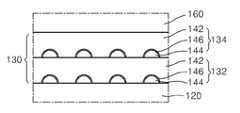
100: 플래쉬 메모리 소자, 102: 반도체 기판, 110: 게이트 적층 구조, 120: 터널링 절연막, 130, 130A, 130B: 전하 트랩막, 132: 제1 하이브리드 트랩막, 134: 제2 하이브리드 트랩막, 136: 캡핑 트랩막, 138: 중간 트랩막, 142: 제1 트랩막, 143: 나노닷 시드, 144: 나노닷, 145: 나노닷 소스 가스, 146: 질화된 표면, 160: 블로킹 절연막, 170: 제어 게이트 전극, 182, 184: 소스/드레인 영역.Reference Numerals 100: flash memory element, 102: semiconductor substrate, 110: gate stacked structure, 120: tunneling insulating film, 130, 130A, 130B: charge trap film, 132: first hybrid trap film, 134: second hybrid trap film, 136: Capping trap film, 138: intermediate trap film, 142: first trap film, 143: nano dot seed, 144: nano dot, 145: nano dot source gas, 146: nitrided surface, 160: blocking insulating film, 170: control gate Electrodes 182, 184: source / drain regions.
본 발명은 반도체 메모리 소자의 제조 방법에 관한 것으로, 특히 전하를 저장하는 트랩 사이트(trap sites)를 가지는 전하 트랩막을 포함하는 플래쉬 메모리 소자 및 그 제조 방법에 관한 것이다.BACKGROUND OF THE
최근, 불휘발성 메모리 소자의 하나로서 전하트랩형 플래쉬 메모리 소자가 개발되어 이동통신 시스템, 메모리 카드 등 다양한 분야에 폭 넓게 채용되고 있다.Recently, a charge trap type flash memory device has been developed as one of nonvolatile memory devices and has been widely used in various fields such as a mobile communication system and a memory card.
통상의 전하 트랩형 플래쉬 메모리 소자는 반도체 기판 위에 터널링 절연막, 전하 트랩막, 블로킹 절연막 및 게이트 전극이 차례로 적층된 게이트 적층 구조를 가진다. 상기 터널링 절연막은 상기 반도체 기판에 형성된 불순물 영역으로 이루어지는 소스 및 드레인에 접촉되어 있으며, 상기 전하 저장층은 상기 터널링 절연막을 통과하는 전하를 저장하는 트랩 사이트를 포함한다. 상기 블로킹 절연막은 전자들이 상기 전하 트랩막의 트랩 사이트에 트랩되는 과정에서 게이트 전극으로 빠져나가는 것을 차단하고 상기 게이트 전극의 전하가 상기 전하 트랩막으로 주입되는 것을 차단하는 역할을 한다.A typical charge trapping flash memory device has a gate stack structure in which a tunneling insulating film, a charge trapping film, a blocking insulating film, and a gate electrode are sequentially stacked on a semiconductor substrate. The tunneling insulating layer is in contact with a source and a drain formed of an impurity region formed in the semiconductor substrate, and the charge storage layer includes a trap site for storing charge passing through the tunneling insulating layer. The blocking insulating layer blocks electrons from escaping to the gate electrode in the process of being trapped in the trap site of the charge trap layer, and blocks the charge of the gate electrode from being injected into the charge trap layer.
상기 구조를 가지는 전하 트랩형 플래쉬 메모리 소자에서는 전압 인가에 의해 상기 터널링 절연막을 통과한 전자들이 상기 전하 트랩막의 트랩 사이트에 트랩되면서 프로그래밍 동작이 이루어진다. 전하 트랩형 플래쉬 메모리 소자에서, Vth (threshold voltage)는 상기 전하 트랩막에 전자가 트랩된 경우와 트랩되지 않은 경우에 따라 변한다. 또한, 상기 전하 트랩막에서 전하의 트랩 밀도가 높아지면 프로그램 및 소거 특성은 향상되나, 리텐션 특성이 나빠진다. 역으로, 상기 전하 트랩막의 트랩 밀도가 낮아지면, 프로그램 및 소거 동작 속도는 감소하나 리텐션 특성은 향상된다. 따라서, 프로그램 및 소거 효율과 리텐션 특성을 동시에 만족시키기는 매우 어렵다.In the charge trapping flash memory device having the above structure, electrons passing through the tunneling insulating film are trapped at the trap site of the charge trap film by voltage application, thereby performing a programming operation. In the charge trapping flash memory device, the threshold voltage (Vth) varies depending on whether electrons are trapped in the charge trap film and when it is not trapped. In addition, if the trap density of the charge in the charge trap film is increased, the program and erase characteristics are improved, but the retention characteristics are deteriorated. Conversely, when the trap density of the charge trap film is lowered, the program and erase operation speeds are reduced, but the retention characteristics are improved. Therefore, it is very difficult to simultaneously satisfy the program and erase efficiency and retention characteristics.
지금까지 플래쉬 메모리의 용량을 증가시키기 위하여 리소그래피 공정을 개선하여 셀 크기를 줄임으로써 셀 당 저장할 수 있는 전하의 수를 늘리고자 하는 시도가 있었다. 그러나, 터널링 절연막에 결함이 발생하게 되면 전하 트랩막에 트랩된 전자들이 쉽게 손실되는 단점이 있다. 특히, 메모리 소자의 스케일링 다운 (scaling down)에 따른 터널링 절연막의 두께가 감소되어 반복적인 읽기/쓰기에 따 른 터널링 절연막의 열화로 인해 전하 트랩막에 저장된 전하가 쉽게 손실될 가능성이 있다. 특히, 실리콘질화막을 전하 트랩막으로 사용하는 SONOS형 메모리 소자의 경우에는 비교적 큰 메모리 윈도우(window)를 확보하는 것은 가능하지만 반복적인 읽기/쓰기 후 터널링 절연막에서의 SILC (stress induced leakage current)로 인한 전하 손실이 매우 크다는 단점이 있다.To date, attempts have been made to increase the number of charges that can be stored per cell by improving the lithography process to reduce the cell size in order to increase the capacity of the flash memory. However, when a defect occurs in the tunneling insulating film, electrons trapped in the charge trap film are easily lost. In particular, the thickness of the tunneling insulating layer due to scaling down of the memory device is reduced, and thus, the charge stored in the charge trap layer may be easily lost due to deterioration of the tunneling insulating layer due to repeated read / write. In particular, in the case of a SONOS type memory device using a silicon nitride film as a charge trapping film, it is possible to secure a relatively large memory window, but due to stress induced leakage current (SILC) in the tunneling insulating film after repeated read / write. The disadvantage is that the charge loss is very large.
본 발명의 목적은 상기한 종래 기술에서의 문제점을 해결하고자 하는 것으로, 스케일링 다운에 따라 축소된 셀 사이즈를 가지는 전하 트랩형 플래쉬 메모리 소자에서 터널링 절연막의 두께가 감소되어도 터널링 절연막의 열화로 인해 전하 트랩막에 저장된 전하가 쉽게 손실되는 것을 방지할 수 있고 전하 저장 능력을 증대시킬 수 있는 구조를 가지는 플래쉬 메모리 소자를 제공하는 것이다.SUMMARY OF THE INVENTION An object of the present invention is to solve the above-mentioned problems in the prior art, and in the charge trapping flash memory device having a reduced cell size due to scaling down, even if the thickness of the tunneling insulating layer is reduced, the charge trapping is caused by deterioration of the tunneling insulating layer. It is to provide a flash memory device having a structure that can easily prevent the loss of charge stored in the film and can increase the charge storage capability.
본 발명의 다른 목적은 스케일링 다운에 따라 축소된 셀 사이즈를 가지는 전하 트랩형 플래쉬 메모리 소자에서 터널링 절연막의 두께가 감소되어도 터널링 절연막의 열화로 인해 전하 트랩막에 저장된 전하가 쉽게 손실되는 것을 방지할 수 있는 새로운 구조의 전하 트랩막을 단순하고 용이한 방법으로 형성할 수 있는 플래쉬 메모리 소자의 제조 방법을 제공하는 것이다.Another object of the present invention is to prevent the loss of charge stored in the charge trap layer easily due to deterioration of the tunneling insulation layer even if the thickness of the tunneling insulation layer is reduced in the charge trapping flash memory device having a reduced cell size due to scaling down. The present invention provides a method of manufacturing a flash memory device capable of forming a charge trap film having a new structure in a simple and easy manner.
상기 목적을 달성하기 위하여, 본 발명에 따른 플래쉬 메모리 소자는 반도체 기판상에 형성된 터널링 절연막과, 상기 터널링 절연막상에 형성된 전하 트랩막과, 상기 전하 트랩막 위에 형성된 블로킹 절연막과, 상기 블로킹 절연막 위에 형성된 제어 게이트 전극을 포함한다. 상기 전하 트랩막은 제1 레벨의 밴드갭 에너지를 가지는 제1 물질로 이루어지는 필름 형태의 제1 트랩막과, 상기 제1 트랩막에 의해 적어도 일부가 포위된 상태에서 소정의 간격을 사이에 두고 상호 이격되어 있고 상기 제1 레벨 보다 더 낮은 밴드갭 에너지를 가지는 제2 물질로 이루어지는 복수의 나노닷을 구비하는 적어도 하나의 하이브리드(hybrid) 트랩막을 포함한다.In order to achieve the above object, a flash memory device according to the present invention comprises a tunneling insulating film formed on a semiconductor substrate, a charge trap film formed on the tunneling insulating film, a blocking insulating film formed on the charge trap film, and formed on the blocking insulating film Control gate electrode. The charge trap film is spaced apart from each other with a predetermined interval therebetween in a state where at least a portion of the first trap film is formed of a film formed of a first material having a first level bandgap energy and surrounded by the first trap film. And at least one hybrid trap film having a plurality of nanodots made of a second material having a lower bandgap energy than the first level.
상기 적어도 하나의 하이브리드 트랩막은 상기 터널링 절연막과 상호 접하도록 형성되어 있는 제1 하이브리드 트랩막을 포함할 수 있다. 이 때, 상기 제1 하이브리드 트랩막에서 상기 복수의 나노닷은 각각 상기 제1 물질 및 상기 터널링 절연막에 의해 완전히 포위될 수 있다.The at least one hybrid trap film may include a first hybrid trap film formed to be in contact with the tunneling insulating film. In this case, the plurality of nanodots in the first hybrid trap layer may be completely surrounded by the first material and the tunneling insulating layer, respectively.
또는, 상기 적어도 하나의 하이브리드 트랩막은 상기 터널링 절연막과 상호 접하도록 형성되어 있는 제1 하이브리드 트랩막과, 상기 제1 하이브리드 트랩막 위에 형성되어 있는 제2 하이브리드 트랩막을 포함할 수 있다. 이 때, 상기 제1 하이브리드 트랩막에 형성되어 있는 복수의 나노닷은 각각 상기 제1 물질 및 상기 터널링 절연막에 의해 완전히 포위될 수 있으며, 상기 제2 하이브리드 트랩막에 형성되어 있는 복수의 나노닷은 상기 제1 물질에 의해 완전히 포위될 수 있다.Alternatively, the at least one hybrid trap film may include a first hybrid trap film formed to be in contact with the tunneling insulating film, and a second hybrid trap film formed on the first hybrid trap film. In this case, the plurality of nanodots formed in the first hybrid trap layer may be completely surrounded by the first material and the tunneling insulating layer, respectively, and the plurality of nanodots formed in the second hybrid trap layer may be It can be completely surrounded by the first material.
상기 하이브리드 트랩막에서 상기 복수의 나노닷은 각각 상기 제1 트랩막 내에서 동일 수평면상에 배열되어 있는 복수의 제1 나노닷을 포함할 수 있다.In the hybrid trap layer, the plurality of nanodots may include a plurality of first nanodots arranged on the same horizontal plane in the first trap layer.
상기 복수의 나노닷은 각각 질화된 표면을 가질 수 있다.The plurality of nanodots may each have a nitrided surface.
상기 전하 트랩막은 상기 하이브리드 트랩막의 표면중 적어도 일부를 덮는 필름 형태의 제2 트랩막을 더 포함할 수 있으며, 상기 제2 트랩막은 상기 제1 트랩 막과 동일한 물질로 구성될 수 있다.The charge trap layer may further include a second trap layer in a film form covering at least a portion of the surface of the hybrid trap layer, and the second trap layer may be formed of the same material as the first trap layer.
상기 전하 트랩막은 상호 상하로 적층되어 있는 제1 하이브리드 트랩막 및 제2 하이브리드 트랩막을 포함할 수 있으며, 상기 제2 트랩막은 상기 제1 하이브리드 트랩막과 상기 제2 하이브리드 트랩막과의 사이에 개재될 수 있다.The charge trap layer may include a first hybrid trap layer and a second hybrid trap layer stacked on top of each other, and the second trap layer may be interposed between the first hybrid trap layer and the second hybrid trap layer. Can be.
상기 하이브리드 트랩막과 상기 블로킹 절연막과의 사이에 개재되어 있는 제3 트랩막을 더 포함할 수 있으며, 상기 제3 트랩막은 상기 제1 트랩막과 동일한 물질로 구성될 수 있다.The display device may further include a third trap layer interposed between the hybrid trap layer and the blocking insulating layer, and the third trap layer may be formed of the same material as the first trap layer.
상기 터널링 절연막과 상기 하이브리드 트랩막과의 사이에 개재되어 있는 제4 트랩막을 더 포함할 수 있으며, 상기 제4 트랩막은 상기 제1 트랩막과 동일한 물질로 구성될 수 있다.A fourth trap layer may be further disposed between the tunneling insulating layer and the hybrid trap layer, and the fourth trap layer may be formed of the same material as the first trap layer.
상기 다른 목적을 달성하기 위하여, 본 발명에 따른 플래쉬 메모리 소자의 제조 방법에서는, 반도체 기판상에 터널링 절연막을 형성한다. 제1 레벨의 밴드갭 에너지를 가지는 제1 물질로 이루어지는 필름 형태의 제1 트랩막과, 상기 제1 트랩막에 의해 적어도 일부가 포위된 상태에서 소정의 간격을 사이에 두고 상호 이격되어 있고 상기 제1 레벨 보다 더 낮은 밴드갭 에너지를 가지는 제2 물질로 이루어지는 복수의 나노닷을 구비하는 적어도 하나의 하이브리드 트랩막을 포함하는 전하 트랩막을 상기 터널링 절연막 위에 형성한다. 상기 전하 트랩막 위에 블로킹 절연막을 형성한다. 상기 블로킹 절연막 위에 제어 게이트 전극을 형성한다.In order to achieve the above another object, in the method of manufacturing a flash memory device according to the present invention, a tunneling insulating film is formed on a semiconductor substrate. A first trap film in the form of a film made of a first material having a bandgap energy of a first level, and spaced apart from each other with a predetermined interval therebetween with at least a portion surrounded by the first trap film; A charge trap film including at least one hybrid trap film having a plurality of nano dots made of a second material having a bandgap energy lower than one level is formed on the tunneling insulating film. A blocking insulating film is formed on the charge trap film. A control gate electrode is formed on the blocking insulating layer.
상기 전하 트랩막을 형성하기 위하여, 상기 터널링 절연막의 위에서 동일 수평면상에 배열되는 복수의 제1 나노닷을 형성한 후, 상기 복수의 제1 나노닷 위에 상기 제1 물질을 증착하여 상기 복수의 제1 나노닷을 포위하는 상기 제1 트랩막을 형성할 수 있다.In order to form the charge trap layer, a plurality of first nanodots are formed on the same horizontal plane on the tunneling insulating layer, and then the first material is deposited on the plurality of first nanodots to form the plurality of first nanodots. The first trap layer surrounding the nano dot may be formed.
상기 복수의 나노닷을 형성하기 위하여, 상기 터널링 절연막 위에 상호 이격되어 있는 복수의 나노닷 시드(seed)를 형성한 후, 상기 나노닷 시드를 성장시켜 상호 이격되어 있는 복수의 제1 나노닷을 형성할 수 있다.In order to form the plurality of nanodots, a plurality of nanodot seeds spaced apart from each other are formed on the tunneling insulating layer, and the nanodot seeds are grown to form a plurality of first nanodots spaced apart from each other. can do.
상기 복수의 제1 나노닷을 형성한 후 상기 복수의 제1 나노닷의 표면을 질화 처리하는 단계를 더 포함할 수 있다.After forming the plurality of first nanodots, the method may further include nitriding a surface of the plurality of first nanodots.
상기 적어도 하나의 하이브리드 트랩막은 상기 터널링 절연막과 상호 접하도록 형성되어 있는 제1 하이브리드 트랩막을 포함할 수 있다. 이 경우, 상기 전하 트랩막을 형성하기 위하여, 상기 터널링 절연막 위에 상기 제1 하이브리드 트랩막을 형성한 후, 상기 제1 하이브리드 트랩막 위에 상기 제1 물질로 이루어지는 필름 형상의 제2 트랩막을 형성할 수 있다.The at least one hybrid trap film may include a first hybrid trap film formed to be in contact with the tunneling insulating film. In this case, in order to form the charge trap layer, the first hybrid trap layer may be formed on the tunneling insulating layer, and then a second film trap formed of the first material may be formed on the first hybrid trap layer.
또한, 상기 적어도 하나의 하이브리드 트랩막은 상기 터널링 절연막과 상호 접하도록 형성되어 있는 제1 하이브리드 트랩막과, 상기 제1 하이브리드 트랩막 위에 형성되어 있는 제2 하이브리드 트랩막을 포함할 수 있다. 이 경우, 상기 제2 하이브리드 트랩막은 상기 제1 하이브리드 트랩막의 상면에 접하도록 형성될 수 있다. 또는, 상기 전하 트랩막을 형성하는 단계는 상기 제1 하이브리드 트랩막을 형성하는 단계와, 상기 제1 하이브리드 트랩막 위에 상기 제1 트랩막과 동일 물질로 이루어지는 필름 형상의 제2 트랩막을 형성하는 단계와, 상기 제2 트랩막 위에 상기 제2 하이브리드 트랩막을 형성하는 단계를 포함할 수 있다.The at least one hybrid trap film may include a first hybrid trap film formed to be in contact with the tunneling insulating film, and a second hybrid trap film formed on the first hybrid trap film. In this case, the second hybrid trap layer may be formed to contact an upper surface of the first hybrid trap layer. Alternatively, the forming of the charge trap layer may include forming the first hybrid trap layer, forming a film-shaped second trap layer formed of the same material as the first trap layer on the first hybrid trap layer; The method may include forming the second hybrid trap layer on the second trap layer.
상기 전하 트랩막을 형성하는 단계는 상기 제2 하이브리드 트랩막 위에 상기 제1 트랩막과 동일 물질로 이루어지는 필름 형상의 제3 트랩막을 형성하는 단계를 더 포함할 수 있다.The forming of the charge trap layer may further include forming a film-shaped third trap layer formed of the same material as the first trap layer on the second hybrid trap layer.
본 발명에 따른 플래쉬 메모리 소자에서는 전하 캡핑층의 제1 트랩막 내에 상기 제1 트랩막 보다 낮은 밴드갭 에너지를 가지는 복수의 나노닷이 형성됨으로써 낮은 트랩 준위에 전자가 포획되어 전하의 리텐션(retention) 특성이 향상된다. 또한, 전하 트랩막 내에 전하 트랩 사이트가 증가하게 되어 소자의 신뢰성을 향상시킬 수 있다.In the flash memory device according to the present invention, a plurality of nanodots having a lower bandgap energy than the first trap layer is formed in the first trap layer of the charge capping layer, so that electrons are trapped at a low trap level, thereby retaining charge. ) The characteristics are improved. In addition, charge trap sites increase in the charge trap film, thereby improving the reliability of the device.
다음에, 본 발명의 바람직한 실시예에 대하여 첨부 도면을 참조하여 상세히 설명한다.Next, a preferred embodiment of the present invention will be described in detail with reference to the accompanying drawings.
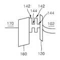
도 1은 본 발명의 바람직한 실시예에 따른 플래쉬 메모리 소자(100)의 요부 구성을 도시한 단면도이다.1 is a cross-sectional view showing the main components of the
도 1을 참조하면, 본 발명에 따른 플래쉬 메모리 소자(100)는 반도체 기판(102)상에 형성된 게이트 적층 구조(110)를 포함한다. 상기 게이트 적층 구조(110)는 상기 반도체 기판(102)상에 형성된 터널링 절연막(120)과, 상기 터널링 절연막(120)상에 형성된 전하 트랩막(130)과, 상기 전하 트랩막(130) 위에 형성된 블로킹 절연막(160)과, 상기 블로킹 절연막(160) 위에 형성된 제어 게이트 전극(170)을 포함한다. 상기 게이트 적층 구조(110)의 양측에서 상기 반도체 기판(102)의 표면에는 소스/드레인 영역(182, 184)이 형성되어 있다.Referring to FIG. 1, the
도 2a는 본 발명에 따른 플래쉬 메모리 소자를 구성할 수 있는 전하 트랩 막(130)의 예시적인 구조를 보다 상세히 설명하기 위하여 도 1의 "II" 부분을 확대 도시한 단면도이다.FIG. 2A is an enlarged cross-sectional view of part “II” of FIG. 1 to explain an exemplary structure of a
도 2a를 참조하면, 상기 전하 트랩막(130)은 상기 터널링 절연막(120) 위에 차례로 형성된 제1 하이브리드(hybrid) 트랩막(132) 및 제2 하이브리드 트랩막(134)을 포함한다. 상기 제1 하이브리드 트랩막(132) 및 제2 하이브리드 트랩막(134)은 각각 제1 레벨의 밴드갭 에너지를 가지는 제1 물질로 이루어지는 필름 형태의 제1 트랩막(142)과, 상기 제1 트랩막(142)에 의해 적어도 일부가 포위된 상태에서 소정의 간격을 사이에 두고 상호 이격되어 있는 복수의 나노닷(144)을 포함한다. 상기 복수의 나노닷(144)은 상기 제1 레벨 보다 더 낮은 밴드갭 에너지를 가지는 제2 물질로 이루어진다. 예를 들면, 상기 제1 트랩막(142)을 구성하는 상기 제1 물질은 Si3N4, HfSiO, HfAlO 및 SiON으로 이루어지는 군에서 선택되는 적어도 하나의 물질로 이루어질 수 있다. 또는, 상기 제1 트랩막(142)은 SRN (Si rich nitride film)막으로 이루어질 수 있다. 여기서, 상기 SRN막은 Si3N4막 내에서의 화학양론적인 Si/N 원자비 보다 더 많은 큰 Si/N 원자비를 가지는 막을 의미한다.Referring to FIG. 2A, the
상기 복수의 나노닷(144)은 각각 반도체 또는 금속으로 이루어질 수 있다. 예를 들면, 상기 복수의 나노닷(144)은 각각 Si, Ge, SiGe와 같은 반도체, 또는 W, WN,TaN, Co, Pt 등과 같은 금속으로 이루어질 수 있다.The plurality of
상기 복수의 나노닷(144)에는 질화된 표면(146)이 형성되어 있다. 상기 질화된 표면(146)은 반드시 필수적인 것은 아니며, 경우에 따라 생략 가능하다.The
상기 복수의 나노닷(144)은 각각 수 나노미터(nm) 내지 수 백 나노미터의 입경 사이즈를 가질 수 있다.The plurality of
도 2a에 예시된 구조에서, 상기 제1 하이브리드 트랩막(132)에서는 상기 복수의 나노닷(144)이 각각 상기 터널링 절연막(120) 및 상기 제1 트랩막(142)에 의해 완전히 포위되어 있게 된다. 그리고, 상기 제2 하이브리드 트랩막(134)에서 상기 복수의 나노닷(144)은 각각 상기 제1 트랩막(142)을 구성하는 제1 물질에 의해 완전히 포위되어 있게 된다.In the structure illustrated in FIG. 2A, in the first
상기 제1 하이브리드 트랩막(132) 및 제2 하이브리드 트랩막(134)에서 상기 복수의 나노닷(144)은 각각 상기 제1 트랩막(142) 내에서 동일 수평면상에 배열되어 있다.In the first
다시 도 1을 참조하면, 상기 터널링 절연막(120)은 SiO2, SiON, HfO2, HfSiO 및 ZrO2로 이루어지는 군에서 선택되는 어느 하나, 또는 이들의 조합으로 이루어질 수 있다. 상기 블로킹 절연막(160)은 Al2O3, SiO2, HfO2, ZrO2, LaO, LaAlO, LaHfO 및 HfAlO로 이루어지는 군에서 선택되는 적어도 하나의 물질로 이루어질 수 있다. 상기 제어 게이트 전극(170)은 TaN, TiN, W, WN, HfN 및 텅스텐 실리사이드로 이루어지는 군에서 선택되는 적어도 하나의 물질로 이루어질 수 있다.Referring back to FIG. 1, the tunneling insulating
도 2a에는 상기 전하 트랩막(130)이 2 개의 하이브리드 트랩막, 즉 상기 제1 하이브리드 트랩막(132) 및 제2 하이브리드 트랩막(134)을 포함하는 것으로 도시되어 있다. 그러나, 본 발명은 이에 한정되지 않는다. 즉, 상기 전하 트랩막(130)이 1 개, 또는 3 개 이상의 하이브리드 트랩막을 포함하는 것도 본 발명의 범위에 포함된다. 또한, 각각의 하이브리드 트랩막 사이에는 상기 제1 트랩막(142)을 구성하는 제1 물질과 동일한 물질로 이루어지는 트랩막이 개재될 수 있다.2A, the
도 2b는 도 2a의 제1 변형에로서, 본 발명에 따른 플래쉬 메모리 소자를 구성할 수 있는 다른 예시적인 전하 트랩막(130A)의 구조를 설명하기 위한 단면도이다.FIG. 2B is a cross-sectional view for explaining the structure of another exemplary
도 2b에 예시된 구성은 도 2a에 예시된 전하 트랩막(130)에서 상기 제2 하이브리드 트랩막(134)과 상기 블로킹 절연막(160)과의 사이에 캡핑용 트랩막(136)이 개재되어 있는 것을 제외하고 도 2a의 구성과 동일하다. 상기 캡핑용 트랩막(136)은 Si3N4, HfSiO, HfAlO, SRN 및 SiON으로 이루어지는 군에서 선택되는 적어도 하나의 물질로 이루어질 수 있다. 상기 캡핑용 트랩막(136)은 상기 제1 트랩막(142)과 동일한 물질로 이루어질 수 있다.The configuration illustrated in FIG. 2B includes a
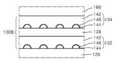
도 2c는 도 2a의 제2 변형예로서, 본 발명에 따른 플래쉬 메모리 소자를 구성할 수 있는 또 다른 예시적인 전하 트랩막(130B)의 구조를 설명하기 위한 단면도이다.FIG. 2C is a cross-sectional view for describing a structure of another exemplary
도 2c에 예시된 구성은 도 2a에 예시된 전하 트랩막(130)에서 상기 제1 하이브리드 트랩막(132)과 상기 제2 하이브리드 트랩막(134)과의 사이에 중간 트랩막(138)이 형성된 것을 제외하고 도 2a의 구성과 동일하다. 상기 중간 트랩막(138)은 Si3N4, HfSiO, HfAlO, SRN 및 SiON으로 이루어지는 군에서 선택되는 적어도 하나 의 물질로 이루어질 수 있다. 상기 제1 하이브리드 트랩막(132)과 상기 제2 하이브리드 트랩막(134)과의 사이에 상기 중간 트랩막(138)이 재개되는 경우, 상기 중간 트랩막(138)은 상기 제1 트랩막(142)과 동일한 물질로 이루어질 수 있다.2C shows that the
또한, 도시하지는 않았으나, 도 2a에 예시된 상기 전하 트랩막(130)은 상기 제1 하이브리드 트랩막(132)과 상기 터널링 절연막(120)과의 사이에 형성된 저부 트랩막(도시 생략)을 더 포함할 수 있다. 상기 저부 트랩막은 Si3N4, HfSiO, HfAlO, SRN 및 SiON으로 이루어지는 군에서 선택되는 적어도 하나의 물질로 이루어질 수 있다. 상기 제1 하이브리드 트랩막(132)과 상기 터널링 절연막(120)과의 사이에 상기 저부 트랩막이 개재되는 경우, 상기 저부 트랩막은 상기 제1 트랩막(142)과 동일한 물질로 이루어질 수 있다.Although not shown, the
상기 저부 트랩막을 형성하지 않는 경우, 도 2a, 도 2b 및 도 2c에 도시된 바와 같이 상기 제1 하이브리드 트랩막(132)은 상기 터널링 절연막(120)과 상호 접하도록 형성되어 있으며, 상기 제1 하이브리드 트랩막(132)에서 상기 복수의 나노닷(144)은 각각 상기 터널링 절연막(120) 및 상기 제1 트랩막(142)에 의해 완전히 포위되어 있게 된다.When the bottom trap layer is not formed, as illustrated in FIGS. 2A, 2B, and 2C, the first
도 3은 도 2a에 예시된 전하 트랩막(130)을 구비한 플래쉬 메모리 소자(100)의 게이트 적층 구조에서의 포텐셜을 보여주는 그래프이다.FIG. 3 is a graph showing the potential of the gate stack structure of the
도 3에 도시한 바와 같이, 터널링 절연막(120)에 인접한 위치에 제1 트랩막(142) 보다 낮은 밴드갭 에너지를 가지는 복수의 나노닷(144)을 형성함으로써 낮 은 트랩 준위에 전자가 포획되어 전하 트랩 에너지가 증가하게 된다. 또한, 전하 트랩막(120) 내에 전하 트랩 사이트가 증가하게 되어 소자의 신뢰성을 향상시킬 수 있다. 특히, Si로 이루어지는 상기 나노닷(144)은 SiO2막의 전도대로부터 약 3 eV 이상 더 깊은 트랩 준위를 가지며, Si3N4막의 전도대로부터 약 1 ∼ 2 eV 이상 더 깊은 트랩 준위를 가진다. 또한, 상기 복수의 나노닷(144)에 의해 상기 전하 트랩막(130) 내에서 트랩된 전하가 불연속적으로 분포되어 있게 되므로 상기 터널링 절연막(120)에 결함이 발생하는 경우에도 상기 결함 위치 근방에서만 전하의 손실이 발생하게 되며 상기 전하 트랩막(130) 전체에는 악영향을 미치지 않는다.As shown in FIG. 3, electrons are trapped at a low trap level by forming a plurality of
도 2a, 도 2b 및 도 2c에 예시된 전하 트랩막(130, 130A, 130B)에서, 상기 복수의 나노닷(144)은 상기 제1 트랩막(142)에 비해 낮은 밴드갭 에너지를 가짐으로써 상기 제1 트랩막(142)에 대하여 포텐셜 웰 (potential well)로 작용한다. 즉, 상기 전하 트랩막(130)에서 복수의 나노닷(144)의 비교적 낮은 Ec (conduction band) 레벨에 의해 낮은 트랩 준위에 전자가 포획되어 전하의 리텐션 특성이 개선될 수 있다.In the charge trap layers 130, 130A, and 130B illustrated in FIGS. 2A, 2B, and 2C, the plurality of
도 2a에 예시된 전하 트랩막(130)을 구성하는 각 요소들의 역할을 설명하면 다음과 같다.The role of each element of the
먼저, 상기 제1 하이브리드 트랩막(132)에 있는 복수의 나노닷(144)은 상기 제1 트랩막(142) 보다 더 낮은 밴드갭 에너지를 가지는 물질로 이루어지므로 깊은 트랩 준위를 제공하여 전하의 리텐션 특성을 향상시킨다. 또한, 상기 복수의 나노 닷(144)에 의해 상기 전하 트랩막(130)에 형성되는 포텐셜 웰이 제공되어 프로그래밍 동작 이후에 열적으로 활성화된 전하가 터널링 절연막(120)으로 빠져 나가게 되는 전하 손실을 줄일 수 있게 된다.First, since the plurality of
상기 제1 하이브리드 트랩막(132)에 있는 제1 트랩막(142)은 상기 복수의 나노닷(144)을 각각 격리시키는 역할을 한다. 따라서, 상기 제1 트랩막(142) 내에 상기 복수의 나노닷(144)을 비교적 높은 밀도로 형성함으로써 전하 저장 능력(charge storage capacity)을 증대시킬 수 있다.The
상기 제2 하이브리드 트랩막(134)에 있는 복수의 나노닷(144)에 의해 상기 전하 트랩막(130) 내에서의 상기 나노닷(144)의 밀도가 증가될 수 있다. 즉, 상기 제2 하이브리드 트랩막(134)에 있는 복수의 나노닷(144)은 상기 전하 트랩막(130) 내에서의 전하 저장 능력을 향상시키는 역할을 한다.The density of the
상기 제2 하이브리드 트랩막(134)에 있는 제1 트랩막(142)은 상기 제2 하이브리드 트랩막(134)에 있는 복수의 나노닷(144) 내에 트랩된 전하의 블로킹 절연막(160)을 통한 전하 손실을 억제해주는 역할을 한다. 또한, 상기 블로킹 절연막(160)을 Al2O3와 같은 금속 산화막으로 형성하는 경우, 상기 블로킹 절연막(160) 형성 공정중에 상기 나노닷(144) 표면이 산화되어 그 특성이 열화되는 것을 방지하는 역할을 한다.The
도 4a 내지 도 4h는 본 발명의 바람직한 실시예에 따른 플래쉬 메모리 소자의 제조 방법을 설명하기 위하여 공정 순서에 따라 도시한 단면도들이다. 도 4a 내 지 도 4h에 있어서, 도 1 및 도 2a에서와 동일한 참조 부호는 동일 요소를 의미한다.4A through 4H are cross-sectional views illustrating a manufacturing method of a flash memory device according to a preferred embodiment of the present invention in order of processing. In Figs. 4A to 4H, the same reference numerals as in Figs. 1 and 2A mean the same elements.
도 4a를 참조하면, 반도체 기판(102)상에 터널링 절연막(120)을 형성한다. 상기 터널링 절연막(120)은 SiO2, SiON, HfO2, HfSiO 및 ZrO2로 이루어지는 군에서 선택되는 어느 하나, 또는 이들의 조합으로 이루어질 수 있으며, 약 20 ∼ 70 Å의 두께로 형성될 수 있다.Referring to FIG. 4A, a tunneling insulating
도 4b를 참조하면, 상기 터널링 절연막(120) 위에 나노닷 소스 가스(145)르르 공급항 상기 터널링 절연막(120) 위에 상호 이격되어 있는 복수의 나노닷 시드(seed)(143)를 형성한다.Referring to FIG. 4B, a plurality of nano dot
상기 복수의 나노닷 시드(143)가 Si로 이루어지는 경우, 상기 나노닷 시드를 형성하기 위하여, 예를 들면 약 500 ∼ 550 ℃의 온도가 유지되는 분위기하에서 상기 터널링 절연막(120) 위에 Si 소스 가스를 소정 시간 예를 들면 약 1 ∼ 2 분 동안 공급할 수 있다. 상기 Si 소스 가스로서 예를 들면 SiH4, Si2H6 및 SiH2Cl2로 이루어지는 군에서 선택되는 어느 하나의 가스를 사용할 수 있다. 상기 복수의 나노닷 시드(143)를 형성하는 동안 예를 들면 약 0.1 내지 10 토르(torr)의 압력을 유지하는 분위기를 조성할 수 있다.When the plurality of nano dot
도 4c를 참조하면, 상기 복수의 나노닷 시드(143)가 형성된 결과물상에 나노닷 소스 가스(145)를 공급하면서 상기 복수의 나노닷 시드(143)를 성장시켜 상호 이격되어 있는 복수의 나노닷(144)을 형성한다. 예를 들면, 상기 복수의 나노닷 시 드(143)가 Si로 이루어지는 경우, 상기 복수의 나노닷(144)은 결정질 Si 닷으로 구성된다.Referring to FIG. 4C, a plurality of nanodots that are spaced apart from each other by growing the plurality of
결정질 Si 닷으로 이루어지는 상기 복수의 나노닷(144)을 형성하기 위하여, 예를 들면 약 570 ∼ 600 의 온도 및 약 0.1 내지 10 토르의 압력이 유지되는 분위기하에서 약 15 ∼ 20 분 동안 상기 복수의 Si 시드가 형성된 결과물상에 Si 소스 가스를 공급하여 상기 Si 시드를 성장시킬 수 있다. 바람직하게는, 상기 복수의 나노닷(144)은 각각 약 5 nm의 입경 사이즈(WD)를 가지도록 형성될 수 있다. 그리고, 상기 복수의 나노닷(144)중 각각의 나노닷(144) 사이의 간격(WG)이 약 5 nm를 유지하도록 형성될 수 있다.In order to form the plurality of
도 4d를 참조하면, 상기 복수의 나노닷(144)의 표면을 질화처리한다. 그 결과, 상기 복수의 나노닷(144)에는 질화된 표면(146)이 형성된다. 상기 복수의 나노닷(144)의 표면을 질화처리함으로써, 후속 공정을 진행하기 전에 웨이퍼의 이송 과정에서 상기 복수의 나노닷(144)의 표면에 원하지 않는 자연산화막이 형성되는 것을 방지할 수 있다. 또한, 상기 복수의 나노닷(144)의 표면을 질화처리하는 동안, 상기 복수의 나노닷(144) 각각의 사이에서 상기 터널링 절연막(120)의 상면에 잔류되어 있을 가능성이 있는 Si 잔류물들이 질화되어 상기 복수의 나노닷(144)이 각각 상호 격리되어 있는 닷 형상을 유지할 수 있다.Referring to FIG. 4D, the surfaces of the plurality of
상기 복수의 나노닷(144) 표면을 질화처리하는 공정은 경우에 따라 생략 가능하다.The process of nitriding the surfaces of the plurality of
도 4e를 참조하면, 상기 복수의 나노닷(144)이 형성된 결과물상에 상기 복수의 나노닷(144)을 포위하는 필름 형상의 제1 트랩막(142)을 형성한다.Referring to FIG. 4E, a
상기 제1 트랩막(142)은 Si3N4, HfSiO, HfAlO, SRN 및 SiON으로 이루어지는 군에서 선택되는 적어도 하나의 물질로 이루어질 수 있다. 상기 제1 트랩막(142)은 상기 터널링 절연막(120) 위에 형성되어 있는 상기 복수의 나노닷(144) 상호간의 간격(WG)과 대략 같은 사이즈의 두께(D1)로 상기 복수의 나노닷(144)를 덮도록 형성되는 것이 바람직하다. 상기 제1 트랩막(142)을 형성하기 위하여 예를 들면 LPCVD (low pressure chemical vapor deposition) 또는 ALD (atomic layer deposition) 공정을 이용할 수 있다.The
도 4f를 참조하면, 앞에서 도 4b 내지 도 4e를 참조하여 설명한 방법과 같은 방법으로 상기 제1 하이브리드 트랩막(132) 위에 제2 하이브리드 트랩막(134)을 형성한다.Referring to FIG. 4F, a second
상기 제2 하이브리드 트랩막(134)은 상기 제1 하이브리드 트랩막(132)과 마찬가지로 질화된 표면(146)을 가지는 복수의 나노닷(144)과 이들을 포위하는 제1 트랩막(142)을 포함한다. 그리고, 상기 제2 하이브리드 트랩막(134)에서, 상기 제1 트랩막(142)은 상기 제1 하이브리드 트랩막(132) 위에 형성되어 있는 상기 복수의 나노닷(144) 상호간의 간격(WG)과 대략 같은 사이즈의 두께(D1)로 상기 복수의 나노닷(144)를 덮도록 형성될 수 있다.Like the first
상기 제1 하이브리드 트랩막(132) 및 제2 하이브리드 트랩막(134)은 전하 트 랩막(130)을 구성한다. 본 예에서는 도 2a에 도시된 전하 트랩막(130) 구조를 형성하는 경우를 예시하였다. 도 2b에 예시된 캡핑용 트랩막(136) 또는 도 2c에 예시된 중간 트랩막(138)을 형성하는 경우, 상기 캡핑용 트랩막(134) 및 상기 중간 트랩막은 각각 LPCVD 또는 ALD 공정을 이용하여 형성될 수 있다.The first
도 4g를 참조하면, 상기 전하 트랩막(130) 위에 블로킹 절연막(160)을 형성한다. 상기 블로킹 절연막(160)은 실리콘 질화막 보다 더 높은 유전 상수를 가지는 고유전막 (high-k film)으로 이루어질 수 있다. 예를 들면, 상기 블로킹 절연막(160)은 금속 산화막, 금속 질화막, 또는 이들의 조합으로 이루어질 수 있다. 상기 블로킹 절연막(160)은 약 40 ∼ 300 Å의 두께로 형성될 수 있다.Referring to FIG. 4G, a blocking insulating
상기 블로킹 절연막(160)은 예를 들면 PVD (physical vapor deposition), ALD (atomic layer deposition), 또는 CVD (chemical vapor deposition) 방법에 의해 형성될 수 있다. 상기 블로킹 절연막(160)은 예를 들면 Al2O3, SiO2, HfO2, ZrO2, LaO, LaAlO, LaHfO 및 HfAlO로 이루어지는 군에서 선택되는 적어도 하나의 물질로 이루어질 수 있다.The blocking insulating
도 4h를 참조하면, 상기 블로킹 절연막(160) 위에 도전 물질을 증착하여 제어 게이트 전극(170)을 형성한다. 상기 제어 게이트 전극(170)은 TaN, TiN, W, WN, HfN 및 텅스텐 실리사이드로 이루어지는 군에서 선택되는 적어도 하나의 물질로 이루어질 수 있다.Referring to FIG. 4H, a conductive material is deposited on the blocking insulating
그 후, 상기 제어 게이트 전극(170), 블로킹 절연막(160), 전하 트랩막(130) 및 터널링 절연막(110)을 차례로 패터닝하여 도 1에 예시된 바와 같은 게이트 적층 구조(150)를 형성한다. 그 후, 상기 게이트 적층 구조(150)의 양측에 노출되어 있는 반도체 기판(102)의 표면에 불순물을 주입하고 열처리하여 도 1에 예시된 바와 같은 소스/드레인 영역(182, 184)을 형성한다.Thereafter, the
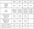
도 5는 본 발명에 따라 다양한 구조를 가지는 플래쉬 메모리 소자의 게이트 적층 구조의 HTS (hot temperature storage) 특성을 대조예의 경우와 비교하여 나타낸 그래프이다.FIG. 5 is a graph illustrating hot temperature storage (HTS) characteristics of a gate stacked structure of a flash memory device having various structures according to the present invention, compared with a case of a comparative example.
도 5에서, 전하 트랩막을 형성하는 데 있어서, 예 1은 SiO2로 이루어지는 터널링 절연막 위에 약 5 nm의 입경을 가지는 복수의 Si 나노 결정 (Si nanocrystal: 도 5에는 "Si NC"로 표시함)을 약 5 nm 간격으로 형성한 후, 그 위에 Si3N4막 (도 5에는 "SiN"으로 표시함)을 LPCVD 공정에 의해 30 Å의 두께로 형성하여 제1 하이브리드 트랩막을 형성하고, 상기 제1 하이브리드 트랩막 위에 다시 약 5 nm의 입경을 가지는 복수의 Si 나노 결정을 약 5 nm 간격으로 형성한 후, 그 위에 Si3N4막을 ALD 공정에 의해 30 Å의 두께로 형성하여 제2 하이브리드 트랩막을 형성한 경우를 나타낸다. 예 2는 제1 하이브리드 트랩막을 구성하는 Si3N4막을 50 Å의 두께로 형성한 것을 제외하고 예 1과 동일하게 형성한 경우를 나타낸다. 예 3은 예 1과 동일하게 형성한 경우를 나타낸다. 예 4는 제2 하이브리드 트랩막을 형성하는 데 있어서 Si NC를 형성한 후 Si3N4막 형성 공정을 생략한 경우를 나타낸다. 예 5는 예 2와 동 일하게 형성한 경우를 나타낸다. 대조예는 전하 트랩막으로서 70 Å 두께의 Si3N4막을 형성한 경우를 나타낸다.In Fig. 5, in forming a charge trap film, Example 1 shows a plurality of Si nanocrystals (Si nanocrystal: denoted as "Si NC" in Fig. 5) having a particle diameter of about 5 nm on a tunneling insulating film made of SiO2 . After forming at intervals of about 5 nm, a Si3 N4 film (denoted as “SiN” in FIG. 5) was formed thereon to a thickness of 30 μs by an LPCVD process to form a first hybrid trap film, wherein the first hybrid trap film was formed. After forming a plurality of Si nanocrystals having a particle diameter of about 5 nm again on the hybrid trap film at about 5 nm intervals, a Si3 N4 film was formed thereon to a thickness of 30 에 by an ALD process to form a second hybrid trap film. The case of formation is shown. Example 2 shows a case where the same form as in Example 1 except that the formed first configuration hybrid trap film Si3 N4 film with a thickness of 50 Å. Example 3 shows the case formed in the same manner as in Example 1. Example 4 shows the case where the Si3 N4 film forming step is omitted after forming the Si NC in forming the second hybrid trap film. Example 5 shows the case formed in the same manner as in Example 2. The control example shows a case where a Si3 N4 film having a thickness of 70 kHz was formed as a charge trapping film.
예 1 내지 예 5와 대조예 각각 전하 트랩막 위에 200 Å의 Al2O3막을 형성한 후 약 1050 ℃의 온도하에서 약 2 분 동안 어닐링하여 블로킹 절연막을 형성하고, 그 위에 약 200 Å의 TaN막을 형성하여 제어 게이트 전극을 형성하였다. 각각의 경우의 게이트 적층 구조는 그 길이 및 폭이 각각 1 ㎛의 사이즈를 가지도록 제작되었다.Examples 1 to 5 and Comparative Examples, respectively, formed a 200 kPa Al2 O3 film on the charge trap film, and then annealed at a temperature of about 1050 ° C. for about 2 minutes to form a blocking insulating film thereon. To form a control gate electrode. In each case, the gate stack structure was manufactured such that its length and width had a size of 1 탆 each.
도 5의 결과를 얻기 위하여, 6 V의 메모리 윈도우를 확보하는 프로그래밍(PGM)/소거(ERS) 전압하에서 1200 사이클 동작 전(NO CYCLE)의 경우와, 1200 사이클 동작 후 200 ℃에서 2 시간 동안 베이크(bake)처리한 경우, 각각 측정되는 ΔVth로 부터 전하 손실을 산출하였다.To obtain the results of FIG. 5, bake for 2 hours at 1200 ° C. before 1200 cycle operation (NO CYCLE) under programming (PGM) / erase (ERS) voltage to ensure a memory window of 6 V and after 1200 cycle operation. In the case of (bake) treatment, the charge loss was calculated from each measured ΔVth.
도 5에 나타낸 바와 같이, 본 발명에 따른 플래쉬 메모리 소자의 게이트 적층 구조를 가지는 예 1 내지 예 5에서 전하 트랩막으로서 Si3N4막으로 이루어지는 필름 형상의 트랩막과, 상기 트랩막에 의해 포위되고 상기 Si3N4막 보다 더 낮은 레벨의 밴드갭 에너지를 가지는 Si 결정질 닷로 이루어지는 복수의 나노닷을 구비하는 하이브리드 트랩막을 형성함으로써 전하 손실을 크게 줄일 수 있다. 특히, 예 1, 예 2, 예 3 및 예 5와 예 4를 비교함으로써 알 수 있는 바와 같이 제2 하이브리드 트랩막에 Si3N4막을 형성한 경우에는 Si3N4막을 생략한 경우 보다 전하 손실을 더 효과적으로 개선할 수 있다. 또한. 예 1과 예 3, 그리고 예 2 와 예 5를 비교하여 알 수 있는 바와 같이, 전하 트랩막의 조건이 동일한 경우, 터널링 절연막의 두께가 증가하면 HTS를 가하기 전에는 전하 손실이 없는 것으로 나타났다. 또한, 예 1 내지 예 5의 경우에는 대조예의 경우에 비해 낮은 동작 전압에서 작동이 가능한 것을 확인할 수 있다.As shown in Fig. 5, in Examples 1 to 5 having a gate stacked structure of the flash memory device according to the present invention, a film-like trap film made of a Si3 N4 film as a charge trap film and surrounded by the trap film Charge loss can be greatly reduced by forming a hybrid trap film having a plurality of nanodots composed of Si crystalline dots having a lower level of bandgap energy than the Si3 N4 film. In particular, as can be seen by comparing Examples 1, 2, 3, and 5 with Example 4, when the Si3 N4 film is formed in the second hybrid trap film, the charge loss is greater than when the Si3 N4 film is omitted. Can be improved more effectively. Also. As can be seen by comparing Examples 1 and 3, and Examples 2 and 5, when the conditions of the charge trapping film are the same, when the thickness of the tunneling insulating film is increased, there is no charge loss until HTS is applied. In addition, in the case of Examples 1 to 5 it can be confirmed that the operation at a lower operating voltage than the case of the control example.
도 6은 본 발명에 따라 다양한 구조를 가지는 플래쉬 메모리 소자의 게이트 적층 구조에서 전하 트랩막의 구조에 따른 HTS 특성과 프로그래밍/소거 동작시의 전계 특성을 평가한 결과를 나타낸 그래프이다.FIG. 6 is a graph illustrating evaluation results of an HTS characteristic according to a structure of a charge trap layer and an electric field characteristic during a programming / erase operation in a gate stacked structure of a flash memory device having various structures according to the present invention.
도 6에서, 전하 트랩막을 형성하는 데 있어서, 예 6은 예 1에서와 동일하게 적용하되, 제1 하이브리드 트랩막을 구성하는 Si3N4막을 50 Å의 두께로 형성하고, 제2 하이브리드 트랩막을 구성하는 Si 나노닷 형성 공정은 생략한 경우를 나타낸다. 예 7은 예 1에서와 동일하게 적용하되, 제1 하이브리드 트랩막에서 Si 나노닷 형성 단계는 생략하고, 제1 하이브리드 트랩막을 구성하는 Si3N4막을 50 Å의 두께로 형성한 경우를 나타낸다. 예 8은 예 1에서와 동일하게 적용하되, 제1 하이브리드 트랩막을 구성하는 Si3N4막을 50 Å의 두께로 형성한 경우를 나타낸다. 예 6, 예 7 및 예 8 각각에 있어서, 터널링 절연막으로서 40 Å의 두께를 가지는 SiO2막을 형성하였다. 예 9는 터널링 절연막으로서 45 Å의 두께를 가지는 SiO2막을 형성한 것을 제외하고 예 8에서와 동일하게 적용하였다.In Fig. 6, in forming the charge trap film, Example 6 is applied in the same manner as in Example 1, except that a Si3 N4 film constituting the first hybrid trap film is formed to a thickness of 50 GPa, and the second hybrid trap film is constituted. The Si nano dot forming process shown in the drawing shows a case where it is omitted. Example 7 is applied in the same manner as in Example 1, except that the Si nano dot forming step in the first hybrid trap film is omitted, and the Si3 N4 film constituting the first hybrid trap film is formed to have a thickness of 50 GPa. Example 8 but is equally applicable as in the example 1, it shows a first case of forming a Si3 N4 film having a thickness of 50 Å constituting one hybrid trap film. In each of Examples 6, 7, and 8, a SiO2 film having a thickness of 40 GPa was formed as the tunneling insulating film. Example 9 was applied in the same manner as in Example 8 except that an SiO2 film having a thickness of 45 GPa was formed as the tunneling insulating film.
도 6의 결과로부터 알 수 있는 바와 같이 예 8에서와 같이 전하 트랩막에서 2 개의 하이브리드 트랩막이 형성된 경우의 HTS 특성 및 프로그래밍/소거 동작시의 전계 특성이 우수한 것을 알 수 있다. 또한, 예 8의 전하 트랩막 조건과 동일한 조건의 전하 트랩막을 가지는 예 9에서, 터널링 절연막 두께를 45 Å으로 증가시켰을 때 소거 동작시의 전하 손실이 없었다.As can be seen from the results of FIG. 6, as in Example 8, it can be seen that the HTS characteristics when two hybrid trap films are formed in the charge trap film and the electric field characteristics in the programming / erase operation are excellent. Further, in Example 9 having the charge trapping film under the same conditions as the charge trapping film of Example 8, there was no charge loss during the erase operation when the tunneling insulating film thickness was increased to 45 kPa.
본 발명에 따른 플래쉬 메모리 소자는 상기 전하 트랩막은 하이브리드 트랩막을 포함한다. 상기 하이브리드 트랩막은 제1 레벨의 밴드갭 에너지를 가지는 제1 물질로 이루어지는 필름 형태의 제1 트랩막과, 상기 제1 트랩막에 의해 적어도 일부가 포위된 상태에서 소정의 간격을 사이에 두고 상호 이격되어 있고 상기 제1 레벨 보다 더 낮은 밴드갭 에너지를 가지는 제2 물질로 이루어지는 복수의 나노닷을 구비한다. 따라서, 본 발명에 따른 플래쉬 메모리 소자에서는 터널링 절연막에 인접한 위치에 제1 트랩막 보다 낮은 밴드갭 에너지를 가지는 복수의 나노닷이 형성됨으로써 낮은 트랩 준위에 전자가 포획되어 전하의 리텐션 특성이 향상된다. 또한, 전하 트랩막 내에 전하 트랩 사이트가 증가하게 되어 소자의 신뢰성을 향상시킬 수 있다. 또한, 전하 트랩막 내에서 전하의 트랩 밀도를 높임으로써 전하 저장 능력을 증대시킬 수 있으며 MLC (multilevel cell) 구현이 가능하다.In the flash memory device according to the present invention, the charge trap layer includes a hybrid trap layer. The hybrid trap film is spaced apart from each other with a predetermined interval between the first trap film in the form of a film made of a first material having a first level bandgap energy, and at least partially surrounded by the first trap film. And a plurality of nanodots made of a second material having a lower bandgap energy than the first level. Accordingly, in the flash memory device according to the present invention, a plurality of nanodots having a lower bandgap energy than the first trap layer is formed at a position adjacent to the tunneling insulating layer, thereby trapping electrons at a low trap level, thereby improving charge retention characteristics. . In addition, charge trap sites increase in the charge trap film, thereby improving the reliability of the device. In addition, by increasing the trap density of the charge in the charge trap layer, it is possible to increase the charge storage capability and to implement a multilevel cell (MLC).
이상, 본 발명을 바람직한 실시예를 들어 상세하게 설명하였으나, 본 발명은 상기 실시예에 한정되지 않고, 본 발명의 기술적 사상 및 범위 내에서 당 분야에서 통상의 지식을 가진 자에 의하여 여러가지 변형 및 변경이 가능하다.In the above, the present invention has been described in detail with reference to preferred embodiments, but the present invention is not limited to the above embodiments, and various modifications and changes by those skilled in the art within the spirit and scope of the present invention. This is possible.
Claims (30)
Translated fromKoreanPriority Applications (4)
| Application Number | Priority Date | Filing Date | Title |
|---|---|---|---|
| KR1020070003395AKR100843229B1 (en) | 2007-01-11 | 2007-01-11 | Flash memory device comprising a charge trap film of a hybrid structure and a manufacturing method thereof |
| US11/776,723US20080169501A1 (en) | 2007-01-11 | 2007-07-12 | Flash memory device with hybrid structure charge trap layer and method of manufacturing same |
| DE102008004290ADE102008004290A1 (en) | 2007-01-11 | 2008-01-07 | Flash memory device with charge trapping layer and method of making the same |
| CNA2008101428213ACN101312216A (en) | 2007-01-11 | 2008-01-11 | Flash memory device with mixing structure charge trapping layer and its manufacture method |
Applications Claiming Priority (1)
| Application Number | Priority Date | Filing Date | Title |
|---|---|---|---|
| KR1020070003395AKR100843229B1 (en) | 2007-01-11 | 2007-01-11 | Flash memory device comprising a charge trap film of a hybrid structure and a manufacturing method thereof |
Publications (1)
| Publication Number | Publication Date |
|---|---|
| KR100843229B1true KR100843229B1 (en) | 2008-07-02 |
Family
ID=39587501
Family Applications (1)
| Application Number | Title | Priority Date | Filing Date |
|---|---|---|---|
| KR1020070003395AExpired - Fee RelatedKR100843229B1 (en) | 2007-01-11 | 2007-01-11 | Flash memory device comprising a charge trap film of a hybrid structure and a manufacturing method thereof |
Country Status (4)
| Country | Link |
|---|---|
| US (1) | US20080169501A1 (en) |
| KR (1) | KR100843229B1 (en) |
| CN (1) | CN101312216A (en) |
| DE (1) | DE102008004290A1 (en) |
Cited By (3)
| Publication number | Priority date | Publication date | Assignee | Title |
|---|---|---|---|---|
| KR101060617B1 (en) | 2008-12-26 | 2011-08-31 | 주식회사 하이닉스반도체 | Nonvolatile Memory Device and Manufacturing Method Thereof |
| US8816424B2 (en) | 2008-12-26 | 2014-08-26 | SK Hynix Inc. | Nonvolatile memory device |
| US9425104B2 (en) | 2013-09-06 | 2016-08-23 | Samsung Electronics Co., Ltd. | Complementary metal oxide semiconductor device and method of manufacturing the same |
Families Citing this family (12)
| Publication number | Priority date | Publication date | Assignee | Title |
|---|---|---|---|---|
| KR100855993B1 (en)* | 2007-04-03 | 2008-09-02 | 삼성전자주식회사 | Charge trap flash memory device and manufacturing method thereof |
| US7691751B2 (en)* | 2007-10-26 | 2010-04-06 | Spansion Llc | Selective silicide formation using resist etchback |
| US9331209B2 (en)* | 2008-01-09 | 2016-05-03 | Faquir C Jain | Nonvolatile memory and three-state FETs using cladded quantum dot gate structure |
| US9153594B2 (en)* | 2008-01-09 | 2015-10-06 | Faquir C. Jain | Nonvolatile memory and three-state FETs using cladded quantum dot gate structure |
| JP5208537B2 (en)* | 2008-02-19 | 2013-06-12 | 株式会社東芝 | Nonvolatile memory element |
| KR20110120661A (en)* | 2010-04-29 | 2011-11-04 | 주식회사 하이닉스반도체 | Nonvolatile Memory Device and Manufacturing Method Thereof |
| KR20130107001A (en)* | 2012-03-21 | 2013-10-01 | 엘지이노텍 주식회사 | Apparatus for deposition |
| US10644016B2 (en)* | 2014-10-30 | 2020-05-05 | Cypress Semiconductor Corporation | Charge-trapping memory device |
| CN105552081B (en)* | 2016-01-22 | 2018-12-04 | 清华大学 | Charge trap-type memory and preparation method thereof |
| CN110047916B (en)* | 2019-03-14 | 2021-02-02 | 南京大学 | Silicon-based charge trapping memory device and preparation method thereof |
| KR20230060963A (en)* | 2021-10-28 | 2023-05-08 | 삼성전자주식회사 | Semiconductor device and electronic system including the same |
| CN119012711B (en)* | 2024-10-24 | 2025-01-10 | 内蒙古工业大学 | A vertically stacked integrated magnetic nanodot memory structure and its preparation method |
Citations (4)
| Publication number | Priority date | Publication date | Assignee | Title |
|---|---|---|---|---|
| JP2004349705A (en) | 2003-05-20 | 2004-12-09 | Samsung Electronics Co Ltd | SONOS memory device |
| JP2005197531A (en) | 2004-01-08 | 2005-07-21 | Macronix Internatl Co Ltd | Nonvolatile semiconductor memory and method of its operation |
| JP2005332924A (en)* | 2004-05-19 | 2005-12-02 | Sony Corp | Nonvolatile semiconductor memory apparatus |
| JP2006196601A (en) | 2005-01-12 | 2006-07-27 | Toshiba Corp | Nonvolatile memory device |
Family Cites Families (6)
| Publication number | Priority date | Publication date | Assignee | Title |
|---|---|---|---|---|
| US6413819B1 (en)* | 2000-06-16 | 2002-07-02 | Motorola, Inc. | Memory device and method for using prefabricated isolated storage elements |
| US7033956B1 (en)* | 2004-11-01 | 2006-04-25 | Promos Technologies, Inc. | Semiconductor memory devices and methods for making the same |
| US7612403B2 (en)* | 2005-05-17 | 2009-11-03 | Micron Technology, Inc. | Low power non-volatile memory and gate stack |
| US7575978B2 (en)* | 2005-08-04 | 2009-08-18 | Micron Technology, Inc. | Method for making conductive nanoparticle charge storage element |
| US7476927B2 (en)* | 2005-08-24 | 2009-01-13 | Micron Technology, Inc. | Scalable multi-functional and multi-level nano-crystal non-volatile memory device |
| US7763511B2 (en)* | 2006-12-29 | 2010-07-27 | Intel Corporation | Dielectric barrier for nanocrystals |
- 2007
- 2007-01-11KRKR1020070003395Apatent/KR100843229B1/ennot_activeExpired - Fee Related
- 2007-07-12USUS11/776,723patent/US20080169501A1/ennot_activeAbandoned
- 2008
- 2008-01-07DEDE102008004290Apatent/DE102008004290A1/ennot_activeWithdrawn
- 2008-01-11CNCNA2008101428213Apatent/CN101312216A/enactivePending
Patent Citations (4)
| Publication number | Priority date | Publication date | Assignee | Title |
|---|---|---|---|---|
| JP2004349705A (en) | 2003-05-20 | 2004-12-09 | Samsung Electronics Co Ltd | SONOS memory device |
| JP2005197531A (en) | 2004-01-08 | 2005-07-21 | Macronix Internatl Co Ltd | Nonvolatile semiconductor memory and method of its operation |
| JP2005332924A (en)* | 2004-05-19 | 2005-12-02 | Sony Corp | Nonvolatile semiconductor memory apparatus |
| JP2006196601A (en) | 2005-01-12 | 2006-07-27 | Toshiba Corp | Nonvolatile memory device |
Cited By (4)
| Publication number | Priority date | Publication date | Assignee | Title |
|---|---|---|---|---|
| KR101060617B1 (en) | 2008-12-26 | 2011-08-31 | 주식회사 하이닉스반도체 | Nonvolatile Memory Device and Manufacturing Method Thereof |
| US8604537B2 (en) | 2008-12-26 | 2013-12-10 | Hynix Semiconductor Inc. | Nonvolatile memory device and method of fabricating the same |
| US8816424B2 (en) | 2008-12-26 | 2014-08-26 | SK Hynix Inc. | Nonvolatile memory device |
| US9425104B2 (en) | 2013-09-06 | 2016-08-23 | Samsung Electronics Co., Ltd. | Complementary metal oxide semiconductor device and method of manufacturing the same |
Also Published As
| Publication number | Publication date |
|---|---|
| CN101312216A (en) | 2008-11-26 |
| DE102008004290A1 (en) | 2008-08-07 |
| US20080169501A1 (en) | 2008-07-17 |
Similar Documents
| Publication | Publication Date | Title |
|---|---|---|
| KR100843229B1 (en) | Flash memory device comprising a charge trap film of a hybrid structure and a manufacturing method thereof | |
| KR100890040B1 (en) | Nonvolatile memory device having a charge trap layer and method of manufacturing same | |
| KR100894098B1 (en) | Nonvolatile memory device having a fast erase speed and improved retention characteristics and method of manufacturing the same | |
| US10079314B2 (en) | Nonvolatile charge trap memory device having a deuterated layer in a multi-layer charge-trapping region | |
| US9553175B2 (en) | SONOS type stacks for nonvolatile charge trap memory devices and methods to form the same | |
| US7012299B2 (en) | Storage layer optimization of a nonvolatile memory device | |
| US20080012065A1 (en) | Bandgap engineered charge storage layer for 3D TFT | |
| KR101033221B1 (en) | Nonvolatile memory device having a charge trap layer and method of manufacturing same | |
| JP4617574B2 (en) | Nonvolatile semiconductor memory device and manufacturing method thereof | |
| US7795159B2 (en) | Charge trap layer for a charge trap semiconductor memory device and method of manufacturing the same | |
| US7820514B2 (en) | Methods of forming flash memory devices including blocking oxide films | |
| KR100819003B1 (en) | Nonvolatile Memory Device Manufacturing Method | |
| US7132337B2 (en) | Charge-trapping memory device and method of production | |
| US20130075804A1 (en) | High density semiconductor memory device and method for manufacturing the same | |
| JP5306604B2 (en) | Binary semiconductor memory device | |
| CN104425503A (en) | Nonvolatile semiconductor memory device, method for manufacturing same, and manufacturing apparatus | |
| KR101083418B1 (en) | Charge trap flash type nonvolatile memory device | |
| KR101052328B1 (en) | Charge-Trap Nonvolatile Memory Devices | |
| KR20080002030A (en) | Method for forming gate structure of nonvolatile memory device | |
| KR20050080864A (en) | Non-volatile memory device and method for fabricating the same | |
| KR20080054709A (en) | Nonvolatile Memory Device and Manufacturing Method Thereof | |
| KR20110078796A (en) | Nonvolatile Memory Device and Manufacturing Method Thereof | |
| KR20110093524A (en) | Nonvolatile Memory Device and Manufacturing Method Thereof |
Legal Events
| Date | Code | Title | Description |
|---|---|---|---|
| A201 | Request for examination | ||
| PA0109 | Patent application | St.27 status event code:A-0-1-A10-A12-nap-PA0109 | |
| PA0201 | Request for examination | St.27 status event code:A-1-2-D10-D11-exm-PA0201 | |
| D13-X000 | Search requested | St.27 status event code:A-1-2-D10-D13-srh-X000 | |
| D14-X000 | Search report completed | St.27 status event code:A-1-2-D10-D14-srh-X000 | |
| E902 | Notification of reason for refusal | ||
| PE0902 | Notice of grounds for rejection | St.27 status event code:A-1-2-D10-D21-exm-PE0902 | |
| E13-X000 | Pre-grant limitation requested | St.27 status event code:A-2-3-E10-E13-lim-X000 | |
| P11-X000 | Amendment of application requested | St.27 status event code:A-2-2-P10-P11-nap-X000 | |
| P13-X000 | Application amended | St.27 status event code:A-2-2-P10-P13-nap-X000 | |
| E701 | Decision to grant or registration of patent right | ||
| PE0701 | Decision of registration | St.27 status event code:A-1-2-D10-D22-exm-PE0701 | |
| GRNT | Written decision to grant | ||
| PR0701 | Registration of establishment | St.27 status event code:A-2-4-F10-F11-exm-PR0701 | |
| PR1002 | Payment of registration fee | St.27 status event code:A-2-2-U10-U11-oth-PR1002 Fee payment year number:1 | |
| PG1601 | Publication of registration | St.27 status event code:A-4-4-Q10-Q13-nap-PG1601 | |
| PR1001 | Payment of annual fee | St.27 status event code:A-4-4-U10-U11-oth-PR1001 Fee payment year number:4 | |
| FPAY | Annual fee payment | Payment date:20120531 Year of fee payment:5 | |
| PR1001 | Payment of annual fee | St.27 status event code:A-4-4-U10-U11-oth-PR1001 Fee payment year number:5 | |
| R18-X000 | Changes to party contact information recorded | St.27 status event code:A-5-5-R10-R18-oth-X000 | |
| FPAY | Annual fee payment | Payment date:20130531 Year of fee payment:6 | |
| PR1001 | Payment of annual fee | St.27 status event code:A-4-4-U10-U11-oth-PR1001 Fee payment year number:6 | |
| LAPS | Lapse due to unpaid annual fee | ||
| PC1903 | Unpaid annual fee | St.27 status event code:A-4-4-U10-U13-oth-PC1903 Not in force date:20140627 Payment event data comment text:Termination Category : DEFAULT_OF_REGISTRATION_FEE | |
| PC1903 | Unpaid annual fee | St.27 status event code:N-4-6-H10-H13-oth-PC1903 Ip right cessation event data comment text:Termination Category : DEFAULT_OF_REGISTRATION_FEE Not in force date:20140627 | |
| P22-X000 | Classification modified | St.27 status event code:A-4-4-P10-P22-nap-X000 | |
| P22-X000 | Classification modified | St.27 status event code:A-4-4-P10-P22-nap-X000 |