KR100841365B1 - Thin film transistor, manufacturing method thereof and organic light emitting display device having same - Google Patents
Thin film transistor, manufacturing method thereof and organic light emitting display device having sameDownload PDFInfo
- Publication number
- KR100841365B1 KR100841365B1KR1020060123078AKR20060123078AKR100841365B1KR 100841365 B1KR100841365 B1KR 100841365B1KR 1020060123078 AKR1020060123078 AKR 1020060123078AKR 20060123078 AKR20060123078 AKR 20060123078AKR 100841365 B1KR100841365 B1KR 100841365B1
- Authority
- KR
- South Korea
- Prior art keywords
- layer
- semiconductor layer
- source
- thin film
- film transistor
- Prior art date
- Legal status (The legal status is an assumption and is not a legal conclusion. Google has not performed a legal analysis and makes no representation as to the accuracy of the status listed.)
- Active
Links
Images


Classifications
- H—ELECTRICITY
- H10—SEMICONDUCTOR DEVICES; ELECTRIC SOLID-STATE DEVICES NOT OTHERWISE PROVIDED FOR
- H10D—INORGANIC ELECTRIC SEMICONDUCTOR DEVICES
- H10D30/00—Field-effect transistors [FET]
- H10D30/60—Insulated-gate field-effect transistors [IGFET]
- H10D30/67—Thin-film transistors [TFT]
- H10D30/6704—Thin-film transistors [TFT] having supplementary regions or layers in the thin films or in the insulated bulk substrates for controlling properties of the device
- H10D30/6713—Thin-film transistors [TFT] having supplementary regions or layers in the thin films or in the insulated bulk substrates for controlling properties of the device characterised by the properties of the source or drain regions, e.g. compositions or sectional shapes
- H—ELECTRICITY
- H01—ELECTRIC ELEMENTS
- H01L—SEMICONDUCTOR DEVICES NOT COVERED BY CLASS H10
- H01L21/00—Processes or apparatus adapted for the manufacture or treatment of semiconductor or solid state devices or of parts thereof
- H01L21/02—Manufacture or treatment of semiconductor devices or of parts thereof
- H01L21/02104—Forming layers
- H01L21/02365—Forming inorganic semiconducting materials on a substrate
- H01L21/02656—Special treatments
- H01L21/02664—Aftertreatments
- H01L21/02667—Crystallisation or recrystallisation of non-monocrystalline semiconductor materials, e.g. regrowth
- H—ELECTRICITY
- H10—SEMICONDUCTOR DEVICES; ELECTRIC SOLID-STATE DEVICES NOT OTHERWISE PROVIDED FOR
- H10D—INORGANIC ELECTRIC SEMICONDUCTOR DEVICES
- H10D30/00—Field-effect transistors [FET]
- H10D30/01—Manufacture or treatment
- H10D30/021—Manufacture or treatment of FETs having insulated gates [IGFET]
- H10D30/031—Manufacture or treatment of FETs having insulated gates [IGFET] of thin-film transistors [TFT]
- H10D30/0312—Manufacture or treatment of FETs having insulated gates [IGFET] of thin-film transistors [TFT] characterised by the gate electrodes
- H10D30/0314—Manufacture or treatment of FETs having insulated gates [IGFET] of thin-film transistors [TFT] characterised by the gate electrodes of lateral top-gate TFTs comprising only a single gate
- H—ELECTRICITY
- H10—SEMICONDUCTOR DEVICES; ELECTRIC SOLID-STATE DEVICES NOT OTHERWISE PROVIDED FOR
- H10D—INORGANIC ELECTRIC SEMICONDUCTOR DEVICES
- H10D30/00—Field-effect transistors [FET]
- H10D30/01—Manufacture or treatment
- H10D30/021—Manufacture or treatment of FETs having insulated gates [IGFET]
- H10D30/031—Manufacture or treatment of FETs having insulated gates [IGFET] of thin-film transistors [TFT]
- H10D30/0321—Manufacture or treatment of FETs having insulated gates [IGFET] of thin-film transistors [TFT] comprising silicon, e.g. amorphous silicon or polysilicon
- H—ELECTRICITY
- H10—SEMICONDUCTOR DEVICES; ELECTRIC SOLID-STATE DEVICES NOT OTHERWISE PROVIDED FOR
- H10D—INORGANIC ELECTRIC SEMICONDUCTOR DEVICES
- H10D30/00—Field-effect transistors [FET]
- H10D30/60—Insulated-gate field-effect transistors [IGFET]
- H10D30/67—Thin-film transistors [TFT]
- H10D30/674—Thin-film transistors [TFT] characterised by the active materials
- H—ELECTRICITY
- H10—SEMICONDUCTOR DEVICES; ELECTRIC SOLID-STATE DEVICES NOT OTHERWISE PROVIDED FOR
- H10D—INORGANIC ELECTRIC SEMICONDUCTOR DEVICES
- H10D62/00—Semiconductor bodies, or regions thereof, of devices having potential barriers
- H10D62/40—Crystalline structures
- H—ELECTRICITY
- H10—SEMICONDUCTOR DEVICES; ELECTRIC SOLID-STATE DEVICES NOT OTHERWISE PROVIDED FOR
- H10D—INORGANIC ELECTRIC SEMICONDUCTOR DEVICES
- H10D86/00—Integrated devices formed in or on insulating or conducting substrates, e.g. formed in silicon-on-insulator [SOI] substrates or on stainless steel or glass substrates
- H10D86/01—Manufacture or treatment
- H10D86/021—Manufacture or treatment of multiple TFTs
- H10D86/0221—Manufacture or treatment of multiple TFTs comprising manufacture, treatment or patterning of TFT semiconductor bodies
- H10D86/0223—Manufacture or treatment of multiple TFTs comprising manufacture, treatment or patterning of TFT semiconductor bodies comprising crystallisation of amorphous, microcrystalline or polycrystalline semiconductor materials
- H10D86/0227—Manufacture or treatment of multiple TFTs comprising manufacture, treatment or patterning of TFT semiconductor bodies comprising crystallisation of amorphous, microcrystalline or polycrystalline semiconductor materials using structural arrangements to control crystal growth, e.g. placement of grain filters
- H—ELECTRICITY
- H10—SEMICONDUCTOR DEVICES; ELECTRIC SOLID-STATE DEVICES NOT OTHERWISE PROVIDED FOR
- H10K—ORGANIC ELECTRIC SOLID-STATE DEVICES
- H10K59/00—Integrated devices, or assemblies of multiple devices, comprising at least one organic light-emitting element covered by group H10K50/00
- H10K59/10—OLED displays
- H10K59/12—Active-matrix OLED [AMOLED] displays
- H10K59/121—Active-matrix OLED [AMOLED] displays characterised by the geometry or disposition of pixel elements
- H10K59/1213—Active-matrix OLED [AMOLED] displays characterised by the geometry or disposition of pixel elements the pixel elements being TFTs
- H—ELECTRICITY
- H10—SEMICONDUCTOR DEVICES; ELECTRIC SOLID-STATE DEVICES NOT OTHERWISE PROVIDED FOR
- H10D—INORGANIC ELECTRIC SEMICONDUCTOR DEVICES
- H10D30/00—Field-effect transistors [FET]
- H10D30/60—Insulated-gate field-effect transistors [IGFET]
- H10D30/67—Thin-film transistors [TFT]
- H10D30/6757—Thin-film transistors [TFT] characterised by the structure of the channel, e.g. transverse or longitudinal shape or doping profile
- H—ELECTRICITY
- H10—SEMICONDUCTOR DEVICES; ELECTRIC SOLID-STATE DEVICES NOT OTHERWISE PROVIDED FOR
- H10K—ORGANIC ELECTRIC SOLID-STATE DEVICES
- H10K59/00—Integrated devices, or assemblies of multiple devices, comprising at least one organic light-emitting element covered by group H10K50/00
- H10K59/10—OLED displays
- H10K59/12—Active-matrix OLED [AMOLED] displays
Landscapes
- Engineering & Computer Science (AREA)
- Microelectronics & Electronic Packaging (AREA)
- Physics & Mathematics (AREA)
- Manufacturing & Machinery (AREA)
- Condensed Matter Physics & Semiconductors (AREA)
- General Physics & Mathematics (AREA)
- Chemical & Material Sciences (AREA)
- Computer Hardware Design (AREA)
- Crystallography & Structural Chemistry (AREA)
- Power Engineering (AREA)
- Geometry (AREA)
- Thin Film Transistor (AREA)
- Recrystallisation Techniques (AREA)
- Electroluminescent Light Sources (AREA)
Abstract
Translated fromKorean
Description
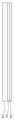
Translated fromKorean도 1a 및 도 1b는 본 발명의 실시 예에 따른 박막트랜지스터의 단면도.1A and 1B are cross-sectional views of a thin film transistor according to an embodiment of the present invention.
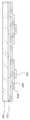
도 1c는 도 1b의 평면도.1C is a top view of FIG. 1B.
도 1d 및 도 1e는 본 발명의 실시 예에 따른 박막트랜지스터의 단면도.1D and 1E are cross-sectional views of a thin film transistor according to an embodiment of the present invention.
도 2a 내지 도 3은 본 발명의 실시 예에 따라 결정화된 다결정 실리콘을 나타낸 도면.2A-3 illustrate polycrystalline silicon crystallized in accordance with an embodiment of the present invention.
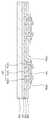
도 4는 본 발명의 실시 예에 따른 유기전계발광표시장치의 단면도.4 is a cross-sectional view of an organic light emitting display device according to an exemplary embodiment of the present invention.
<도면 주요부호에 대한 부호의 설명><Description of Symbols for Major Symbols in Drawings>
100 : 기판101 : 버퍼층100
102 : 비정질 실리콘층103 : 게이트 절연막102
104 : 게이트 전극105a : 양극104:
105b : 음극106 : 전원105b: cathode 106: power supply
107 : 반도체층108 : 층간 절연막107: semiconductor layer 108: interlayer insulating film
109a,109b : 소스/드레인 전극109a and 109b: source / drain electrodes
본 발명은 박막트랜지스터와 그 제조방법 및 이를 구비한 유기전계발광표시장치에 관한 것으로, 보다 자세하게는 줄열 방법에 의해 박막트랜지스터를 제조하는데 있어서, 박막트랜지스터의 특성을 향상시킬 수 있는 박막트랜지스터와 그 제조방법 및 이를 구비한 유기전계발광표시장치에 관한 것이다.The present invention relates to a thin film transistor, a method for manufacturing the same, and an organic light emitting display device having the same. More particularly, in manufacturing a thin film transistor by a Joule heat method, a thin film transistor and a manufacturing method thereof can be improved. A method and an organic light emitting display device having the same.
최근에 음극선관(cathode ray tube)과 같이 무겁고, 크기가 크다는 종래의 표시 소자의 단점을 해결하는 액정 표시 장치(liquid crystal display device), 유기전계발광표시장치(organic light emitting diode display device) 또는 PDP(plasma display panel) 등과 같은 평판형 표시 장치가 주목 받고 있다.Recently, a liquid crystal display device, an organic light emitting diode display device, or a PDP that solves the shortcomings of a conventional display device, such as a cathode ray tube, which is heavy and large. Attention has been paid to flat panel display devices such as plasma display panels.
상기와 같은 평판형 표시 장치에 이용되는 박막트랜지스터는 주어진 신호에 따라 고속으로 작동하는 특성 또는 기판 전체에 걸쳐 균일한 특성이 요구되어지는데, 이러한 박막트랜지스터의 특성을 만족시키기 위해서는 박막트랜지스터의 반도체층의 특성을 제어하는 것이 가장 중요하다.The thin film transistor used in the flat panel display device needs to operate at high speed according to a given signal or to have uniform characteristics throughout the substrate. In order to satisfy the characteristics of the thin film transistor, the semiconductor layer of the thin film transistor It is most important to control the characteristics.
상기 반도체층은 비정질 실리콘을 폴리 실리콘으로 결정화하여 사용하는데, 이러한 방법으로는 고상 결정화법(Solid Phase Crystallization : SPC), 엑시머 레이저 결정화법(Eximer Laser Annealing : ELA), 금속 유도 결정화법(Metal Induced Crystallization : MIC) 및 금속 유도 측면 결정화법(Metal Induced Lateral Crystallization : MILC) 등이 있는데, 상기 고상 결정화법은 비정질 실리콘층을 박막트랜지스터 사용되는 디스플레이 소자의 기판을 형성하는 물질인 유리의 변형 온도인 약 700℃ 이하의 온도에서 수 시간 내지 수십 시간에 걸쳐 어닐링하는 방법이고, 엑시머 레이저 결정화법은 엑시머 레이저를 실리콘층에 주사하여 매우 짧은 시간동안 국부적으로 높은 온도로 가열하여 결정화하는 방법이고, 금속 유도 결정화법은 니켈, 팔라듐, 금, 알루미늄 등의 금속을 비정질 실리콘층과 접촉시키거나 주입하여 상기 금속에 의해 비정질 실리콘층이 다결정 실리콘층으로 상변화가 유도되는 현상을 이용하는 방법이고, 금속 유도 측면 결정화법은 금속과 실리콘이 반응하여 생성된 실리사이드가 측면으로 계속하여 전파되면서 순차적으로 실리콘의 결정화를 유도하는 방법이다.The semiconductor layer is used by crystallizing amorphous silicon with polysilicon, such as solid phase crystallization (SPC), Eximer Laser Annealing (ELA), Metal Induced Crystallization (Metal Induced Crystallization) : MIC) and Metal Induced Lateral Crystallization (MILC). The solid phase crystallization method is about 700, which is a deformation temperature of glass, which is a material for forming a substrate of a display device using an amorphous silicon layer as a thin film transistor. It is a method of annealing for several hours to several tens of hours at a temperature of less than ℃, the excimer laser crystallization method is a method of crystallizing the excimer laser by heating to a locally high temperature for a very short time and the metal-induced crystallization method Metals such as silver nickel, palladium, gold, aluminum, and the like It is a method of using the phenomenon that the phase change is induced by the metal to the polycrystalline silicon layer by stimulating or injecting, the metal-induced side crystallization method is the silicide generated by the reaction of the metal and silicon is continuously propagated to the side It is a method of inducing crystallization of silicon sequentially.
그러나, 상기의 고상 결정화법은 기판을 고온에서 장시간 열처리함으로서, 기판에 손상이 가해지는 문제점이 있고, 상기 엑시머 레이저 결정화법은 레이저 설비가 고가일 뿐만 아니라, 많은 유지비가 소요된다는 문제점이 있고, 상기 금속 유도 결정화법 내지 금속 유도 측면 결정화법은 다결정 실리콘층으로 결정화하는데 너무 많은 시간이 필요하다는 문제점이 있다.However, the above-mentioned solid-phase crystallization method has a problem that damage is caused to the substrate by heat-treating the substrate at a high temperature for a long time, and the excimer laser crystallization method has a problem that the laser equipment is not only expensive but also requires a large maintenance cost. The metal induced crystallization method or the metal induced side crystallization method has a problem that it takes too much time to crystallize into a polycrystalline silicon layer.
따라서, 본 발명은 상기와 같은 종래 기술의 제반 단점과 문제점을 해결하기 위한 것으로, 줄열 결정화법에 의해 박막트랜지스터를 제조하는데 있어서, 박막트 랜지스터의 특성을 향상시킬 수 있는 박막트랜지스터와 그 제조방법 및 이를 구비한 유기전계발광표시장치를 제공함에 본 발명의 목적이 있다.Accordingly, the present invention is to solve the above disadvantages and problems of the prior art, in manufacturing a thin film transistor by the Joule thermal crystallization method, a thin film transistor and a method for manufacturing the thin film transistor can be improved And it is an object of the present invention to provide an organic light emitting display device having the same.
본 발명의 상기 목적은 기판; 상기 기판 상에 위치하며, 채널 영역 및 소스/드레인 영역을 포함하는 반도체층; 상기 반도체층 상에 위치하는 게이트 절연막; 상기 게이트 절연막 상에 위치하며, 상기 채널 영역에 대응되는 게이트 전극; 상기 게이트 전극 상에 위치하는 층간 절연막; 상기 반도체층의 소스/드레인 영역에 전기적으로 연결되는 소스/드레인 전극을 포함하며, 상기 채널 영역은 다결정 실리콘이고, 상기 소스/드레인 영역은 비정질 실리콘인 것을 특징으로 하는 박막트랜지스터에 의해 달성된다.The object of the present invention is a substrate; A semiconductor layer on the substrate, the semiconductor layer including a channel region and a source / drain region; A gate insulating layer on the semiconductor layer; A gate electrode on the gate insulating layer and corresponding to the channel region; An interlayer insulating layer on the gate electrode; And a source / drain electrode electrically connected to the source / drain region of the semiconductor layer, wherein the channel region is polycrystalline silicon, and the source / drain region is amorphous silicon.
본 발명의 상기 목적은 기판을 제공하고, 상기 기판 상에 비정질 실리콘층을 형성하고, 상기 비정질 실리콘층을 패터닝하여 반도체층을 형성하고, 상기 기판 전면에 게이트 절연막을 형성하고, 상기 게이트 절연막 상에 상기 반도체층의 일정 영역과 대응되도록 게이트 전극을 형성하고, 상기 반도체층의 일정 영역을 게이트 전극의 저항열로 결정화하고, 상기 기판 전면에 층간 절연막을 형성하고, 상기 반도체층에 전기적으로 연결되는 소스/드레인 전극을 형성하는 것을 포함하는 것을 특징으로 하는 박막트랜지스터의 제조방법에 의해 달성된다.The object of the present invention is to provide a substrate, to form an amorphous silicon layer on the substrate, to form a semiconductor layer by patterning the amorphous silicon layer, to form a gate insulating film on the entire surface of the substrate, on the gate insulating film A gate electrode is formed to correspond to a predetermined region of the semiconductor layer, the predetermined region of the semiconductor layer is crystallized by a resistance row of the gate electrode, an interlayer insulating layer is formed on the entire surface of the substrate, and a source electrically connected to the semiconductor layer. It is achieved by a method for manufacturing a thin film transistor, characterized in that it comprises forming a / drain electrode.
또한, 본 발명의 상기 목적은 기판; 상기 기판 상에 위치하며, 다결정 실리콘인 채널 영역 및 비정질 실리콘인 소스/드레인 영역을 포함하는 반도체층; 상기 반도체층 상에 위치하는 게이트 절연막; 상기 게이트 절연막 상에 위치하며, 상기 채널 영역에 대응되는 게이트 전극; 상기 게이트 전극 상에 위치하는 층간 절연막; 상기 반도체층의 소스/드레인 영역에 전기적으로 연결되는 소스/드레인 전극; 상기 소스/드레인 전극에 전기적으로 연결된 제 1 전극 및 상기 제 1 전극 상에 위치한 유기막층 및 제 2 전극을 포함하는 것을 특징으로 하는 유기전계발광표시장치에 의해 달성된다.In addition, the above object of the present invention; A semiconductor layer on the substrate, the semiconductor layer comprising a channel region that is polycrystalline silicon and a source / drain region that is amorphous silicon; A gate insulating layer on the semiconductor layer; A gate electrode on the gate insulating layer and corresponding to the channel region; An interlayer insulating layer on the gate electrode; A source / drain electrode electrically connected to a source / drain region of the semiconductor layer; The organic light emitting display device includes a first electrode electrically connected to the source / drain electrode, and an organic layer and a second electrode on the first electrode.
본 발명의 상기 목적과 기술적 구성 및 그에 따른 작용효과에 관한 자세한 사항은 본 발명의 바람직한 실시예를 도시하고 있는 도면을 참조한 이하 상세한 설명에 의해 보다 명확하게 이해될 것이다. 또한 도면들에 있어서, 층 및 영역의 길이, 두께등은 편의를 위하여 과장되어 표현될 수도 있다. 명세서 전체에 걸쳐서 동일한 참조번호들은 동일한 구성요소들을 나타낸다.Details of the above object and technical configuration of the present invention and the effects thereof according to the present invention will be more clearly understood by the following detailed description with reference to the drawings showing preferred embodiments of the present invention. In the drawings, the length, thickness, etc. of layers and regions may be exaggerated for convenience. Like numbers refer to like elements throughout.
도 1a 및 도 1b는 본 발명의 실시 예에 따른 박막트랜지스터의 단면도이고, 도 1c는 도 1b의 평면도이고, 도 1d 및 도 1e는 본 발명의 실시 예에 따른 박막트랜지스터의 단면도이다.1A and 1B are cross-sectional views of a thin film transistor according to an embodiment of the present invention, FIG. 1C is a plan view of FIG. 1B, and FIGS. 1D and 1E are cross-sectional views of a thin film transistor according to an embodiment of the present invention.
도 1a를 참조하면, 절연 유리 또는 플라스틱과 같은 투명한 기판(100) 상에 버퍼층(101)을형성한다. 상기 버퍼층(101)은 기판 하부에서 침투하는 수분 또는 불순물의 확산을 방지하거나 결정화 시 열의 전달 속도를 조절함으로써, 후속 공정에서 형성될 다결정 실리콘층의 결정화가 잘 이루어질 수 있도록 하는 역할을 하며, 실리콘 산화막, 실리콘 질화막 또는 이들의 다중층으로 이루어질 수 있다.Referring to FIG. 1A, a
이어서, 상기 버퍼층(101) 상에 비정질 실리콘층(102)을 형성한다. 이때, 상 기 비정질 실리콘층은 화학적 기상 증착법(Chemical Vapor Deposition) 또는 물리적 기상 증착법(Physical Vapor Deposition)을 이용할 수 있다. 또한, 상기 비정질 실리콘층을 형성할 때, 또는 형성한 후에 탈수소 처리하여 수소의 농도를 낮추는 공정을 진행할 수 있다.Subsequently, an
이어, 상기 비정질 실리콘층(102)을 패터닝하여 반도체층(107)을 형성한다. 이때, 상기 반도체층(107)은 후속 결정화 공정 시, 게이트 전극 하부에 위치하게 되어 결정화 되는 다결정 실리콘층 영역을 채널 영역으로 사용하고, 그 이외의 비정질 실리콘층 영역은 추후 소스/드레인 영역이 될 수 있다. 따라서, 상기 반도체층(107)을 형성할 때, 소스/드레인이 될 영역의 마진을 생각하여 반도체층(107)을 형성한다.Subsequently, the
이어서, 도 1b를 참조하면, 상기 기판(100) 전면에 게이트 절연막(103)을 형성한다. 상기 게이트 절연막(103)은후속 결정화 공정에서 비정질 실리콘층(102)의 표면을 보호하는 역할을 하고 열이 유출되는 것을 방지하는 역할을 할 수 있다.Subsequently, referring to FIG. 1B, a
이때, 상기 게이트 절연막(103)은 화학적기상 증착법(Chemical Vapor Deposition) 또는 물리적 기상 증착법(Physical Vapor Deposition)을 이용하여 실리콘 산화막 또는 실리콘 질화막으로 형성될 수 있다.In this case, the
여기서, 상기 게이트 절연막(103)은 800 내지 1500Å의 두께로 형성되는 것이 바람직하다. 상기 게이트 절연막(103)의 두께는 이후 박막트랜지스터가 완성되었을 때 게이트 절연막으로의 바람직한 특성을 고려할 때 800Å이상인 것이 바람직하지만, 후속 줄열 결정화 공정 시 저항열이 반도체층으로 전도되는 특성을 고려할 때 1500Å이하인 것이 바람직하다.Here, the
이어서, 상기 게이트 절연막(103) 상에 알루미늄(Al), 은(Ag), 티타늄(Ti), 텅스텐(W) 또는 몰리브덴(Mo)으로 이루어진 단일층 또는 이들의 다중층으로 게이트 전극용 금속층을 형성한다. 이어, 상기 게이트 전극용 금속층을 식각하여 게이트 전극(104)을 형성한다.Subsequently, a metal layer for the gate electrode is formed on the
상기 게이트 전극(104)은 인가된 파워에 의해 저항열(Joule Heating)을 발생하는 금속의 역할을 하게 된다. 따라서, 상기 게이트 전극(104)은 인가된 파워에 의해 저항열(즉, 상기 게이트 전극은 파워, 즉, 전기에 의해 열을 발생시키는 박막히터의 역할을 하게 된다.)을 발생시키게 되어 고온의 열을 발생시키게 되는데, 상기와 같이, 저항열 금속으로 적당한 저항을 갖고 고온에서도 산화되지 않으며, 열전도성이 우수한 금속을 사용하는 것이 바람직하다.The
이어서, 도 1b의 평면도인 도 1c를 참조하면, 상기 게이트 전극(104)의 양 끝단 영역에 소정의 파워를 인가시키기 위해 양극(105a) 및 음극(105b)을 형성하고 파워(W)를 인가할 수 있는 전원(106)과 연결한다. 이때, 상기 게이트 전극 패턴이 직사각형인 경우, 장축의 양쪽 가장자리를 가리키는 것이고, 상기 양극(105a) 또는 음극(105b)은 장축의 양쪽 가장자리 중 어느 한 곳에 형성된다.Subsequently, referring to FIG. 1C, which is a plan view of FIG. 1B, the
이어서, 상기 전원에 의해 공급된 파워가 양극(105a) 및 음극(105b)을 통해 상기 게이트 전극(104)에 주입되고, 상기 게이트 전극(104)에 주입된 파워는 게이트 전극(104)의 저항에 의해 저항열을 발생하게 된다. 특히, 상기 저항열은 상기 게이트 전극(104)에서 주로 발생한다.Subsequently, power supplied by the power source is injected into the
이때, 상기 발생하는 저항열은 인가되는 파워에 비례하게 되는데 상기 파워는 하기의 [수학식 1]과 같이 전압(V)과 전류(A)의 곱인 파워(W)에 비례하게 된다.In this case, the generated resistance heat is proportional to the applied power, which is proportional to the power W that is the product of the voltage V and the current A as shown in Equation 1 below.
저항열(Joule Heating) ∝ 파워(W) = 전압(V) × 전류(A)Joule Heating ∝ Power (W) = Voltage (V) × Current (A)
상기 파워의 인가에 의해 발생한 저항열은 게이트 전극(104)의 하부의 게이트 절연막(103)으로 전도되고, 상기 게이트 절연막(103)으로 전도된 저항열은 상기 게이트 절연막(103) 하부의 비정질 실리콘층(102)으로 전도되게 된다. 이때, 전도되는 저항열은 상기의 [수학식 1]에서 설명한 바와 같이 인가된 파워에 선형적으로 비례하게 된다.The resistance heat generated by the application of the power is conducted to the
상기 전도된 저항열은 상기 비정질 실리콘층(102)을 가열하여 수 초 내지 수십 초 내에 비정질 실리콘층의 온도를 700 내지 900℃까지 상승시킬 수 있다. 이때, 온도가 상승한 게이트 전극(104) 하부에 위치한 비정질 실리콘층(102)은 다결정 실리콘층으로 결정화하게 된다. 이때, 상기 게이트 전극(104) 하부 이외에 형성된 비정질 실리콘층(102)은 결정화되지 않는다.The conducted resistance heat may heat the
도 2a 내지 도 2d는 결정화 시간에 따른 비정질 실리콘층의 결정화되는 모습을 나타내는 사진이다.2A to 2D are photographs showing the crystallization state of the amorphous silicon layer according to the crystallization time.
본 발명의 일 실시 예에서는 상기 게이트 전극(104)의 선폭을 300㎛로 형성하고, 전압을 175V로 인가하였다.In an embodiment of the present invention, the line width of the
먼저, 도 2a는 결정화 시간이 20초일 때, 결정화의 핵이 국부적으로 형성되 면서 결정화의 초기 모습을 볼 수 있다. 이어, 도 2b는 결정화 시간이 40초일 때의 모습으로 결정화가 점차 진행되고 있는 것을 볼 수 있다. 다음, 도 2c는 결정화 시간이 60초일 때의 모습으로 40초 때보다 더 많이 결정화된 것을 볼 수 있다. 또한, 도 2d는 결정화 시간이 80초일 때의 모습으로 게이트 전극(104)의 하부에비정질 실리콘층이 대부분 다결정화 된 것을 볼 수 있다. 그러나, 상기 도 2a 내지 도 2d에서 보는 바와 같이, 게이트 전극(104)이 형성되지 않은 영역의 비정질 실리콘층은 결정화되지 않은 것을 알 수 있다.First, Figure 2a, when the crystallization time is 20 seconds, the nuclei of crystallization can be formed locally, the initial appearance of the crystallization can be seen. Subsequently, it can be seen that the crystallization is gradually progressing in the state where the crystallization time is 40 seconds. Next, FIG. 2C shows that the crystallization time is 60 seconds, more crystallization than when 40 seconds. In addition, FIG. 2D illustrates that the crystallization time is 80 seconds, in which the amorphous silicon layer is mostly polycrystallized in the lower portion of the
즉, 상기 게이트 전극(104)이 형성된 영역 하부에 위치한 비정질 실리콘층은 추후 채널 영역으로 작용할 수 있기 때문에 상기 게이트 전극(104)을 형성하는 위치를 조절하여 원하는 부위에서 선택적으로 결정화할 수 있다. 이에 따라, 높은 이동도를 요구하는 드라이버 회로(driver IC) 영역을 결정화하여 시스템 온 글라스(System On Glass)를 구현할 수 있는 이점이 있다.That is, since the amorphous silicon layer located under the region where the
또한, 짧은 시간 내에 결정화를 이룰 수 있기 때문에 유리 기판을 사용할 경우에 기판의 변형을 방지할 수 있는 이점이 있다.In addition, since crystallization can be achieved within a short time, there is an advantage in that deformation of the substrate can be prevented when using a glass substrate.
다음, 도 3은 본 발명의 실시 예에 따라 결정화된 다결정 실리콘층을 나타낸 도면이다.3 is a view showing a polycrystalline silicon layer crystallized according to an embodiment of the present invention.
도 3을 참조하면, 본 실시 예에 따라 줄열 방법을 사용하여 결정화된 다결정 실리콘층은 약 40㎛ 정도의 매우 큰 그레인(grain)을 갖는 것을 알 수 있다. 따라서, 그레인 바운더리(Grain Boundary)가 적은 다결정 실리콘을 제조할 수 있고 이에 따라 박막트랜지스터의 특성을 우수하게 할 수 있는 이점이 있다.Referring to FIG. 3, it can be seen that the polycrystalline silicon layer crystallized using the Joule heat method according to the present embodiment has a very large grain of about 40 μm. Therefore, it is possible to manufacture polycrystalline silicon with low grain boundary and thus, there is an advantage in that the characteristics of the thin film transistor can be improved.
다음, 도 1d를 참조하면, 결정화 공정이 끝난 후에, 상기 기판(100) 전면에 상기 게이트 전극(104)을 마스크로 사용하여 도전형의 불순물 이온을 일정량 주입하여 소스/드레인 영역(107a,107b) 및 채널 영역(107c)을 형성한다. 이때, 상기 불순물 이온으로는 p형 불순물 또는 n형 불순물을 이용하여 박막트랜지스터를 형성할 수 있는데, 상기 p형 불순물은 붕소(B), 알루미늄(Al), 갈륨(Ga) 및 인듐(In)으로 이루어진 군에서 선택할 수 있고, 상기 n형 불순물은 인(P), 비소(As) 및 안티몬(Sb) 등으로 이루어진 군에서 선택할 수 있다.Next, referring to FIG. 1D, after the crystallization process is finished, a predetermined amount of conductive impurity ions are implanted using the
따라서, 이전 공정에서 게이트 전극(104) 하부에 위치한 반도체층 영역을 결정화하였으므로, 상기 게이트 전극 하부에 위치한 채널 영역(107c)은 다결정 실리콘이고, 그 외의 소스/드레인 영역(107a,107b)는 비정질 실리콘이 된다.Therefore, since the semiconductor layer region under the
이어서, 도 1e를 참조하면, 상기 게이트 절연막(103) 및 게이트 전극(104)을 포함하는 기판(100) 전면에 층간 절연막(108)을 형성한다.Subsequently, referring to FIG. 1E, an
이어, 상기 층간 절연막(108) 및 게이트 절연막(103)의 일정 영역을 식각하여 콘택홀을 형성하고, 상기 콘택홀을 통해 상기 반도체층(107)의 소스/드레인 영역(107a,107b)에 전기적으로 연결되는 소스/드레인 전극(109a,109b)을 형성하여, 본 발명의 실시 예에 따른 박막트랜지스터를 완성한다.Subsequently, a predetermined region of the interlayer insulating
상기와 같이, 본 발명의 실시 예에 따른 박막트랜지스터는 원하는 부위에 선택적으로 비정질 실리콘을 다결정 실리콘으로 결정화할 수 있어 이에 따라, 높은 이동도를 요구하는 드라이버 회로(driver IC) 영역을 결정화하여 시스템 온 글라스(System On Glass)를 구현할 수 있는 이점이 있다.As described above, the thin film transistor according to the embodiment of the present invention can selectively crystallize amorphous silicon into polycrystalline silicon at a desired portion, thereby crystallizing a driver IC region requiring high mobility and thereby turning on the system. There is an advantage that can implement a glass (System On Glass).
또한, 짧은 시간 내에 결정화를 이룰 수 있기 때문에 유리 기판을 사용할 경우에 기판의 변형을 방지할 수 있는 이점이 있다.In addition, since crystallization can be achieved within a short time, there is an advantage in that deformation of the substrate can be prevented when using a glass substrate.
또한, 그레인 바운더리(Grain Boundary)가 적은 다결정 실리콘을 제조할 수 있어 박막트랜지스터의 특성을 우수하게 할 수 있는 이점이 있다.In addition, it is possible to manufacture polycrystalline silicon with low grain boundaries, which has the advantage of improving the characteristics of the thin film transistor.
이어서, 도 4는 본 발명의 실시 예에 따른 유기전계발광표시장치의 단면도이다.4 is a cross-sectional view of an organic light emitting display device according to an exemplary embodiment of the present invention.
도 4를 참조하면, 상기 기판(100) 전면에 평탄화막(115)을 형성한다. 상기 평탄화막(115)은 유기막 또는 무기막으로 형성하거나 이들의 복합막으로 형성할 수 있다. 상기 평탄화막(115)을 무기막으로 형성하는 경우는 SOG(spin on glass)를 사용하여 형성하는 것이 바람직하고, 유기막으로 형성하는 경우 아크릴계 수지, 폴리이미드계 수지 또는 BCB(benzocyclobutene)을 사용하여 형성하는 것이 바람직하다.Referring to FIG. 4, the
이때, 상기 평탄화막(115)을 식각하여 상기 소오스/드레인 전극(109a, 109b) 중 어느 하나를 노출시키는 비어홀을 형성하고, 상기 소오스/드레인 전극(109a, 109b) 중 어느 하나와 연결되는 제 1 전극(116)을 형성한다. 상기 제 1 전극(116)은 상기 비아홀의 바닥에 위치하여 상기 노출된 소오스/드레인 전극(109a, 109b) 중 어느 하나에 접하고, 상기 평탄화막(115) 상으로 연장된다. 상기 제 1 전극(116)은 ITO(Indium Tin Oxide) 또는 IZO(Indium Zinc Oxide)를 사용할 수 있다.In this case, the
이어서, 상기 제 1 전극(116)을 포함한 기판(100) 전면에 화소정의막(117)을 형성하되, 상기 제 1 전극(116)이 위치한 비아홀을 충분히 채울 수 있을 정도의 두께로 형성한다. 상기 화소정의막(117)은 유기막 또는 무기막으로 형성할 수 있으 나, 바람직하게는 유기막으로 형성한다. 더욱 바람직하게는 상기 화소정의막(117)은 BCB(benzocyclobutene), 아크릴계 고분자 및 폴리이미드로 이루어진 군에서 선택되는 하나이다. 상기 화소정의막(117)은 유동성(flowability)이 뛰어나므로 상기 기판 전체에 평탄하게 형성할 수 있다.Subsequently, the
이때, 상기 화소정의막(117)을 식각하여 상기 제 1 전극(116)을 노출시키는 개구부를 형성하고, 상기 개구부를 통해 노출된 제 1 전극(116) 상에 유기막층(118)을 형성한다. 상기 유기막층(118)은 적어도 발광층을 포함하며, 정공주입층, 정공수송층, 전자수송층 또는 전자주입층중 어느 하나 이상의 층을 추가로 포함할 수 있다.In this case, the
이어서, 상기 기판(100) 전면에 제 2 전극(119)을 형성한다. 상기 제 2 전극(119)은 투과전극으로 투명하면서 일함수가 낮은 Mg, Ag, Al, Ca 및 이들의 합금으로 사용할 수 있다.Subsequently, a
따라서, 상기와 같이 본 발명의 실시 예에 따른 유기전계발광표시장치를 완성한다.Therefore, the organic light emitting display device according to the embodiment of the present invention is completed as described above.
본 발명은 이상에서 살펴본 바와 같이 바람직한 실시예를 들어 도시하고 설명하였으나, 상기한 실시 예에 한정되지 아니하며 본 발명의 정신을 벗어나지 않는 범위 내에서 당해 발명이 속하는 기술분야에서 통상의 지식을 가진 자에 의해 다양한 변경과 수정이 가능할 것이다.The present invention has been shown and described with reference to the preferred embodiments as described above, but is not limited to the above embodiments and those skilled in the art without departing from the spirit of the present invention. Various changes and modifications will be possible.
따라서, 본 발명의 박막트랜지스터와 그 제조방법 및 이를 구비한 유기전계발광표시장치는 결정성이 우수한 다결정 실리콘층을 제조할 수 있고, 이에 따라 우수한 특성을 지닌 박막트랜지스터를 제공할 수 있는 효과가 있다.Accordingly, the thin film transistor of the present invention, a method of manufacturing the same, and an organic light emitting display device having the same can produce a polycrystalline silicon layer having excellent crystallinity, thereby providing a thin film transistor having excellent characteristics. .
또한, 드라이버 회로(driver IC) 영역을 결정화하여 시스템 온 글라스(System On Glass)를 구현할 수 있는 이점이 있다.In addition, there is an advantage that the system on glass (System On Glass) can be implemented by crystallizing the driver IC (driver IC) region.
또한, 짧은 시간 내에 결정화를 이룰 수 있기 때문에 유리 기판을 사용할 경우에 기판의 변형을 방지할 수 있는 이점이 있다.In addition, since crystallization can be achieved within a short time, there is an advantage in that deformation of the substrate can be prevented when using a glass substrate.
Claims (18)
Translated fromKoreanPriority Applications (3)
| Application Number | Priority Date | Filing Date | Title |
|---|---|---|---|
| KR1020060123078AKR100841365B1 (en) | 2006-12-06 | 2006-12-06 | Thin film transistor, manufacturing method thereof and organic light emitting display device having same |
| US11/987,998US20080135847A1 (en) | 2006-12-06 | 2007-12-06 | Thin film transistor, method of fabricating the same, and organic light emitting display device including the same |
| US12/906,830US8053297B2 (en) | 2006-12-06 | 2010-10-18 | Method of fabricating a thin film transistor using joule heat from the gate electrode to form a crystallized channel region |
Applications Claiming Priority (1)
| Application Number | Priority Date | Filing Date | Title |
|---|---|---|---|
| KR1020060123078AKR100841365B1 (en) | 2006-12-06 | 2006-12-06 | Thin film transistor, manufacturing method thereof and organic light emitting display device having same |
Publications (2)
| Publication Number | Publication Date |
|---|---|
| KR20080051618A KR20080051618A (en) | 2008-06-11 |
| KR100841365B1true KR100841365B1 (en) | 2008-06-26 |
Family
ID=39496905
Family Applications (1)
| Application Number | Title | Priority Date | Filing Date |
|---|---|---|---|
| KR1020060123078AActiveKR100841365B1 (en) | 2006-12-06 | 2006-12-06 | Thin film transistor, manufacturing method thereof and organic light emitting display device having same |
Country Status (2)
| Country | Link |
|---|---|
| US (2) | US20080135847A1 (en) |
| KR (1) | KR100841365B1 (en) |
Cited By (4)
| Publication number | Priority date | Publication date | Assignee | Title |
|---|---|---|---|---|
| US8987719B2 (en) | 2012-09-18 | 2015-03-24 | Samsung Display Co., Ltd. | Organic light emitting diode display |
| KR20160093659A (en)* | 2013-12-02 | 2016-08-08 | 가부시키가이샤 한도오따이 에네루기 켄큐쇼 | Display device |
| WO2016206151A1 (en)* | 2015-06-24 | 2016-12-29 | 深圳市华星光电技术有限公司 | Manufacturing method for low temperature poly-silicon tft substrate structure, and low temperature poly-silicon tft substrate structure |
| WO2017217620A1 (en)* | 2016-06-16 | 2017-12-21 | 한국과학기술원 | Field-effect transistor capable of self-recovery against radiation damage and damage recovery system thereof |
Families Citing this family (6)
| Publication number | Priority date | Publication date | Assignee | Title |
|---|---|---|---|---|
| KR100976593B1 (en)* | 2008-07-25 | 2010-08-17 | 주식회사 엔씰텍 | Thin film transistor and its manufacturing method |
| KR101535821B1 (en)* | 2009-05-29 | 2015-07-13 | 엘지디스플레이 주식회사 | Method for fabricating thin film transistor and method for fabricating display device having thin film transistor |
| KR102447828B1 (en) | 2015-12-22 | 2022-09-28 | 삼성디스플레이 주식회사 | Organic light emitting display device |
| CN105870198B (en) | 2016-05-11 | 2020-03-31 | 京东方科技集团股份有限公司 | Thin film transistor and manufacturing method thereof, array substrate and manufacturing method thereof, and display device |
| CN107482065A (en)* | 2017-09-15 | 2017-12-15 | 京东方科技集团股份有限公司 | Method for manufacturing thin film transistor, thin film transistor, backplane, and display device |
| CN110071125A (en)* | 2019-05-05 | 2019-07-30 | 京东方科技集团股份有限公司 | TFT backplate and preparation method thereof, OLED display panel |
Citations (2)
| Publication number | Priority date | Publication date | Assignee | Title |
|---|---|---|---|---|
| KR100202122B1 (en)* | 1993-07-26 | 1999-07-01 | 야스카와 히데아키 | Thin film semiconductor device and manufacturing method thereof and display system |
| KR100280171B1 (en)* | 1995-09-14 | 2001-02-01 | 니시무로 타이죠 | Non-single-crystal semiconductor device (thin film transistor), liquid crystal display device using the same and manufacturing method thereof |
Family Cites Families (7)
| Publication number | Priority date | Publication date | Assignee | Title |
|---|---|---|---|---|
| US5231297A (en)* | 1989-07-14 | 1993-07-27 | Sanyo Electric Co., Ltd. | Thin film transistor |
| US5569936A (en)* | 1993-03-12 | 1996-10-29 | Semiconductor Energy Laboratory Co., Ltd. | Semiconductor device employing crystallization catalyst |
| US5684365A (en)* | 1994-12-14 | 1997-11-04 | Eastman Kodak Company | TFT-el display panel using organic electroluminescent media |
| JP2002176180A (en)* | 2000-12-06 | 2002-06-21 | Hitachi Ltd | Thin film semiconductor device and method of manufacturing the same |
| US7232714B2 (en)* | 2001-11-30 | 2007-06-19 | Semiconductor Energy Laboratory Co., Ltd. | Semiconductor device |
| KR100611225B1 (en)* | 2003-11-22 | 2006-08-10 | 삼성에스디아이 주식회사 | Thin film transistor and its manufacturing method |
| KR100623693B1 (en) | 2004-08-25 | 2006-09-19 | 삼성에스디아이 주식회사 | Method of manufacturing thin film transistor |
- 2006
- 2006-12-06KRKR1020060123078Apatent/KR100841365B1/enactiveActive
- 2007
- 2007-12-06USUS11/987,998patent/US20080135847A1/ennot_activeAbandoned
- 2010
- 2010-10-18USUS12/906,830patent/US8053297B2/enactiveActive
Patent Citations (2)
| Publication number | Priority date | Publication date | Assignee | Title |
|---|---|---|---|---|
| KR100202122B1 (en)* | 1993-07-26 | 1999-07-01 | 야스카와 히데아키 | Thin film semiconductor device and manufacturing method thereof and display system |
| KR100280171B1 (en)* | 1995-09-14 | 2001-02-01 | 니시무로 타이죠 | Non-single-crystal semiconductor device (thin film transistor), liquid crystal display device using the same and manufacturing method thereof |
Cited By (5)
| Publication number | Priority date | Publication date | Assignee | Title |
|---|---|---|---|---|
| US8987719B2 (en) | 2012-09-18 | 2015-03-24 | Samsung Display Co., Ltd. | Organic light emitting diode display |
| KR20160093659A (en)* | 2013-12-02 | 2016-08-08 | 가부시키가이샤 한도오따이 에네루기 켄큐쇼 | Display device |
| KR102220450B1 (en) | 2013-12-02 | 2021-02-25 | 가부시키가이샤 한도오따이 에네루기 켄큐쇼 | Display device |
| WO2016206151A1 (en)* | 2015-06-24 | 2016-12-29 | 深圳市华星光电技术有限公司 | Manufacturing method for low temperature poly-silicon tft substrate structure, and low temperature poly-silicon tft substrate structure |
| WO2017217620A1 (en)* | 2016-06-16 | 2017-12-21 | 한국과학기술원 | Field-effect transistor capable of self-recovery against radiation damage and damage recovery system thereof |
Also Published As
| Publication number | Publication date |
|---|---|
| US8053297B2 (en) | 2011-11-08 |
| KR20080051618A (en) | 2008-06-11 |
| US20080135847A1 (en) | 2008-06-12 |
| US20110033992A1 (en) | 2011-02-10 |
Similar Documents
| Publication | Publication Date | Title |
|---|---|---|
| KR100841365B1 (en) | Thin film transistor, manufacturing method thereof and organic light emitting display device having same | |
| CN101315883B (en) | Manufacturing method of polysilicon layer, TFT and its manufacturing method, and OLED display device | |
| KR100864884B1 (en) | Thin film transistor, manufacturing method thereof and organic light emitting display device having same | |
| JP5043781B2 (en) | THIN FILM TRANSISTOR, ORGANIC ELECTROLUMINESCENT DISPLAY DEVICE HAVING THE SAME, AND METHOD FOR MANUFACTURING THE SAME | |
| KR100882909B1 (en) | Thin film transistor, manufacturing method thereof, organic light emitting display device comprising same, and manufacturing method thereof | |
| US8530290B2 (en) | Thin film transistor, method of fabricating the same, and organic light emitting diode display device including the same | |
| KR100965260B1 (en) | Thin film transistor, manufacturing method thereof and organic light emitting display device having same | |
| JP5301971B2 (en) | THIN FILM TRANSISTOR, ITS MANUFACTURING METHOD, AND ORGANIC ELECTROLUMINESCENT DISPLAY DEVICE INCLUDING THE SAME | |
| EP2117048B1 (en) | Thin film transistor, method of fabricating the same and organic light emitting diode display device having the same | |
| CN101630693A (en) | Thin film transistor, method of fabricating the same, and organic light emitting diode display device including the thin film transistor | |
| KR101146995B1 (en) | Method for formation of crystalline silicon layer and method for formation of thin film transistor using the same | |
| JP2006178449A (en) | Thin film transistor display panel | |
| KR100504538B1 (en) | Method For Crystallizing Amorphous Layer And Method For Fabricating Liquid Crystal Display Device By Using Said Method | |
| KR101009432B1 (en) | Thin film transistor and its manufacturing method | |
| KR101043788B1 (en) | Method for manufacturing polycrystalline silicon film and method for manufacturing thin film transistor including same | |
| KR101043785B1 (en) | Thin film transistor and its manufacturing method | |
| CN104733537B (en) | Thin film transistor (TFT) and manufacturing method and its organic LED display device | |
| KR20060084487A (en) | Method of manufacturing thin film transistor array panel | |
| KR20100078861A (en) | Thin film transistor, fabricating method of the thin film transistor, and organic lighting emitting diode display device comprising the same |
Legal Events
| Date | Code | Title | Description |
|---|---|---|---|
| A201 | Request for examination | ||
| PA0109 | Patent application | Patent event code:PA01091R01D Comment text:Patent Application Patent event date:20061206 | |
| PA0201 | Request for examination | ||
| E902 | Notification of reason for refusal | ||
| PE0902 | Notice of grounds for rejection | Comment text:Notification of reason for refusal Patent event date:20071024 Patent event code:PE09021S01D | |
| E701 | Decision to grant or registration of patent right | ||
| PE0701 | Decision of registration | Patent event code:PE07011S01D Comment text:Decision to Grant Registration Patent event date:20080416 | |
| PG1501 | Laying open of application | ||
| GRNT | Written decision to grant | ||
| PR0701 | Registration of establishment | Comment text:Registration of Establishment Patent event date:20080619 Patent event code:PR07011E01D | |
| PR1002 | Payment of registration fee | Payment date:20080620 End annual number:3 Start annual number:1 | |
| PG1601 | Publication of registration | ||
| PR1001 | Payment of annual fee | Payment date:20110527 Start annual number:4 End annual number:4 | |
| PR1001 | Payment of annual fee | Payment date:20120604 Start annual number:5 End annual number:5 | |
| FPAY | Annual fee payment | Payment date:20130530 Year of fee payment:6 | |
| PR1001 | Payment of annual fee | Payment date:20130530 Start annual number:6 End annual number:6 | |
| FPAY | Annual fee payment | Payment date:20140530 Year of fee payment:7 | |
| PR1001 | Payment of annual fee | Payment date:20140530 Start annual number:7 End annual number:7 | |
| FPAY | Annual fee payment | Payment date:20150601 Year of fee payment:8 | |
| PR1001 | Payment of annual fee | Payment date:20150601 Start annual number:8 End annual number:8 | |
| FPAY | Annual fee payment | Payment date:20160530 Year of fee payment:9 | |
| PR1001 | Payment of annual fee | Payment date:20160530 Start annual number:9 End annual number:9 | |
| FPAY | Annual fee payment | Payment date:20170601 Year of fee payment:10 | |
| PR1001 | Payment of annual fee | Payment date:20170601 Start annual number:10 End annual number:10 | |
| FPAY | Annual fee payment | Payment date:20190529 Year of fee payment:12 | |
| PR1001 | Payment of annual fee | Payment date:20190529 Start annual number:12 End annual number:12 | |
| PR1001 | Payment of annual fee | Payment date:20200527 Start annual number:13 End annual number:13 | |
| PR1001 | Payment of annual fee | Payment date:20210601 Start annual number:14 End annual number:14 | |
| PR1001 | Payment of annual fee | Payment date:20220523 Start annual number:15 End annual number:15 | |
| PR1001 | Payment of annual fee | Payment date:20230524 Start annual number:16 End annual number:16 | |
| PR1001 | Payment of annual fee | Payment date:20240523 Start annual number:17 End annual number:17 |