KR100841153B1 - Liquid Crystal Devices and Electronics - Google Patents
Liquid Crystal Devices and ElectronicsDownload PDFInfo
- Publication number
- KR100841153B1 KR100841153B1KR1020070007969AKR20070007969AKR100841153B1KR 100841153 B1KR100841153 B1KR 100841153B1KR 1020070007969 AKR1020070007969 AKR 1020070007969AKR 20070007969 AKR20070007969 AKR 20070007969AKR 100841153 B1KR100841153 B1KR 100841153B1
- Authority
- KR
- South Korea
- Prior art keywords
- liquid crystal
- common electrode
- electrode
- insulating film
- pixel electrode
- Prior art date
- Legal status (The legal status is an assumption and is not a legal conclusion. Google has not performed a legal analysis and makes no representation as to the accuracy of the status listed.)
- Active
Links
Images


Classifications
- G—PHYSICS
- G02—OPTICS
- G02F—OPTICAL DEVICES OR ARRANGEMENTS FOR THE CONTROL OF LIGHT BY MODIFICATION OF THE OPTICAL PROPERTIES OF THE MEDIA OF THE ELEMENTS INVOLVED THEREIN; NON-LINEAR OPTICS; FREQUENCY-CHANGING OF LIGHT; OPTICAL LOGIC ELEMENTS; OPTICAL ANALOGUE/DIGITAL CONVERTERS
- G02F1/00—Devices or arrangements for the control of the intensity, colour, phase, polarisation or direction of light arriving from an independent light source, e.g. switching, gating or modulating; Non-linear optics
- G02F1/01—Devices or arrangements for the control of the intensity, colour, phase, polarisation or direction of light arriving from an independent light source, e.g. switching, gating or modulating; Non-linear optics for the control of the intensity, phase, polarisation or colour
- G02F1/13—Devices or arrangements for the control of the intensity, colour, phase, polarisation or direction of light arriving from an independent light source, e.g. switching, gating or modulating; Non-linear optics for the control of the intensity, phase, polarisation or colour based on liquid crystals, e.g. single liquid crystal display cells
- G02F1/133—Constructional arrangements; Operation of liquid crystal cells; Circuit arrangements
- G02F1/1333—Constructional arrangements; Manufacturing methods
- G02F1/1343—Electrodes
- G02F1/134309—Electrodes characterised by their geometrical arrangement
- G—PHYSICS
- G02—OPTICS
- G02F—OPTICAL DEVICES OR ARRANGEMENTS FOR THE CONTROL OF LIGHT BY MODIFICATION OF THE OPTICAL PROPERTIES OF THE MEDIA OF THE ELEMENTS INVOLVED THEREIN; NON-LINEAR OPTICS; FREQUENCY-CHANGING OF LIGHT; OPTICAL LOGIC ELEMENTS; OPTICAL ANALOGUE/DIGITAL CONVERTERS
- G02F1/00—Devices or arrangements for the control of the intensity, colour, phase, polarisation or direction of light arriving from an independent light source, e.g. switching, gating or modulating; Non-linear optics
- G02F1/01—Devices or arrangements for the control of the intensity, colour, phase, polarisation or direction of light arriving from an independent light source, e.g. switching, gating or modulating; Non-linear optics for the control of the intensity, phase, polarisation or colour
- G02F1/13—Devices or arrangements for the control of the intensity, colour, phase, polarisation or direction of light arriving from an independent light source, e.g. switching, gating or modulating; Non-linear optics for the control of the intensity, phase, polarisation or colour based on liquid crystals, e.g. single liquid crystal display cells
- G02F1/133—Constructional arrangements; Operation of liquid crystal cells; Circuit arrangements
- G02F1/1333—Constructional arrangements; Manufacturing methods
- G02F1/1343—Electrodes
- G—PHYSICS
- G02—OPTICS
- G02F—OPTICAL DEVICES OR ARRANGEMENTS FOR THE CONTROL OF LIGHT BY MODIFICATION OF THE OPTICAL PROPERTIES OF THE MEDIA OF THE ELEMENTS INVOLVED THEREIN; NON-LINEAR OPTICS; FREQUENCY-CHANGING OF LIGHT; OPTICAL LOGIC ELEMENTS; OPTICAL ANALOGUE/DIGITAL CONVERTERS
- G02F1/00—Devices or arrangements for the control of the intensity, colour, phase, polarisation or direction of light arriving from an independent light source, e.g. switching, gating or modulating; Non-linear optics
- G02F1/01—Devices or arrangements for the control of the intensity, colour, phase, polarisation or direction of light arriving from an independent light source, e.g. switching, gating or modulating; Non-linear optics for the control of the intensity, phase, polarisation or colour
- G02F1/13—Devices or arrangements for the control of the intensity, colour, phase, polarisation or direction of light arriving from an independent light source, e.g. switching, gating or modulating; Non-linear optics for the control of the intensity, phase, polarisation or colour based on liquid crystals, e.g. single liquid crystal display cells
- G02F1/133—Constructional arrangements; Operation of liquid crystal cells; Circuit arrangements
- G02F1/1333—Constructional arrangements; Manufacturing methods
- G02F1/1335—Structural association of cells with optical devices, e.g. polarisers or reflectors
- G02F1/133509—Filters, e.g. light shielding masks
- G02F1/133512—Light shielding layers, e.g. black matrix
- G—PHYSICS
- G02—OPTICS
- G02F—OPTICAL DEVICES OR ARRANGEMENTS FOR THE CONTROL OF LIGHT BY MODIFICATION OF THE OPTICAL PROPERTIES OF THE MEDIA OF THE ELEMENTS INVOLVED THEREIN; NON-LINEAR OPTICS; FREQUENCY-CHANGING OF LIGHT; OPTICAL LOGIC ELEMENTS; OPTICAL ANALOGUE/DIGITAL CONVERTERS
- G02F1/00—Devices or arrangements for the control of the intensity, colour, phase, polarisation or direction of light arriving from an independent light source, e.g. switching, gating or modulating; Non-linear optics
- G02F1/01—Devices or arrangements for the control of the intensity, colour, phase, polarisation or direction of light arriving from an independent light source, e.g. switching, gating or modulating; Non-linear optics for the control of the intensity, phase, polarisation or colour
- G02F1/13—Devices or arrangements for the control of the intensity, colour, phase, polarisation or direction of light arriving from an independent light source, e.g. switching, gating or modulating; Non-linear optics for the control of the intensity, phase, polarisation or colour based on liquid crystals, e.g. single liquid crystal display cells
- G02F1/133—Constructional arrangements; Operation of liquid crystal cells; Circuit arrangements
- G02F1/1333—Constructional arrangements; Manufacturing methods
- G02F1/1343—Electrodes
- G02F1/134309—Electrodes characterised by their geometrical arrangement
- G02F1/134372—Electrodes characterised by their geometrical arrangement for fringe field switching [FFS] where the common electrode is not patterned
- G—PHYSICS
- G02—OPTICS
- G02F—OPTICAL DEVICES OR ARRANGEMENTS FOR THE CONTROL OF LIGHT BY MODIFICATION OF THE OPTICAL PROPERTIES OF THE MEDIA OF THE ELEMENTS INVOLVED THEREIN; NON-LINEAR OPTICS; FREQUENCY-CHANGING OF LIGHT; OPTICAL LOGIC ELEMENTS; OPTICAL ANALOGUE/DIGITAL CONVERTERS
- G02F1/00—Devices or arrangements for the control of the intensity, colour, phase, polarisation or direction of light arriving from an independent light source, e.g. switching, gating or modulating; Non-linear optics
- G02F1/01—Devices or arrangements for the control of the intensity, colour, phase, polarisation or direction of light arriving from an independent light source, e.g. switching, gating or modulating; Non-linear optics for the control of the intensity, phase, polarisation or colour
- G02F1/13—Devices or arrangements for the control of the intensity, colour, phase, polarisation or direction of light arriving from an independent light source, e.g. switching, gating or modulating; Non-linear optics for the control of the intensity, phase, polarisation or colour based on liquid crystals, e.g. single liquid crystal display cells
- G02F1/133—Constructional arrangements; Operation of liquid crystal cells; Circuit arrangements
- G02F1/136—Liquid crystal cells structurally associated with a semi-conducting layer or substrate, e.g. cells forming part of an integrated circuit
- G02F1/1362—Active matrix addressed cells
- G02F1/136213—Storage capacitors associated with the pixel electrode
- G—PHYSICS
- G02—OPTICS
- G02F—OPTICAL DEVICES OR ARRANGEMENTS FOR THE CONTROL OF LIGHT BY MODIFICATION OF THE OPTICAL PROPERTIES OF THE MEDIA OF THE ELEMENTS INVOLVED THEREIN; NON-LINEAR OPTICS; FREQUENCY-CHANGING OF LIGHT; OPTICAL LOGIC ELEMENTS; OPTICAL ANALOGUE/DIGITAL CONVERTERS
- G02F1/00—Devices or arrangements for the control of the intensity, colour, phase, polarisation or direction of light arriving from an independent light source, e.g. switching, gating or modulating; Non-linear optics
- G02F1/01—Devices or arrangements for the control of the intensity, colour, phase, polarisation or direction of light arriving from an independent light source, e.g. switching, gating or modulating; Non-linear optics for the control of the intensity, phase, polarisation or colour
- G02F1/13—Devices or arrangements for the control of the intensity, colour, phase, polarisation or direction of light arriving from an independent light source, e.g. switching, gating or modulating; Non-linear optics for the control of the intensity, phase, polarisation or colour based on liquid crystals, e.g. single liquid crystal display cells
- G02F1/133—Constructional arrangements; Operation of liquid crystal cells; Circuit arrangements
- G02F1/136—Liquid crystal cells structurally associated with a semi-conducting layer or substrate, e.g. cells forming part of an integrated circuit
- G02F1/1362—Active matrix addressed cells
- G02F1/136227—Through-hole connection of the pixel electrode to the active element through an insulation layer
Landscapes
- Physics & Mathematics (AREA)
- Nonlinear Science (AREA)
- Mathematical Physics (AREA)
- Chemical & Material Sciences (AREA)
- Crystallography & Structural Chemistry (AREA)
- General Physics & Mathematics (AREA)
- Optics & Photonics (AREA)
- Geometry (AREA)
- Liquid Crystal (AREA)
Abstract
Translated fromKorean
Description
Translated fromKorean도 1은 본 발명의 실시예 1에 따른 액정 장치의 구성을 모식적으로 나타내는 평면도,1 is a plan view schematically showing the configuration of a liquid crystal device according to a first embodiment of the present invention;
도 2는 실시예 1에 따른 화소 구성 등을 나타내는 부분 확대 평면도,2 is a partially enlarged plan view illustrating a pixel configuration and the like according to the first embodiment;
도 3은 도 2의 절단선 A-A'에 따른 서브 화소의 부분 단면도,3 is a partial cross-sectional view of the sub-pixel along the cutting line A-A 'of FIG.
도 4는 비교예에 따른 화소 구성 등을 나타내는 부분 확대 평면도,4 is a partially enlarged plan view illustrating a pixel configuration and the like according to a comparative example;
도 5는 도 4의 절단선 B-B'에 따른 서브 화소의 부분 단면도,FIG. 5 is a partial cross-sectional view of a sub pixel along a cutting line B-B ′ of FIG. 4;
도 6은 실시예 2에 따른 화소 구성 등을 나타내는 부분 확대 평면도,6 is a partially enlarged plan view illustrating a pixel configuration and the like according to the second embodiment;
도 7은 도 6의 절단선 C-C'에 따른 서브 화소의 부분 단면도,FIG. 7 is a partial cross-sectional view of a sub pixel along a cutting line C-C ′ of FIG. 6;
도 8은 실시예 2의 작용 효과를 설명하는 소자 기판의 부분 단면도,8 is a partial cross-sectional view of an element substrate for explaining the effect of Example 2;
도 9는 본 발명의 액정 장치를 적용한 전자기기의 예를 나타내는 도면.9 is a diagram showing an example of an electronic apparatus to which the liquid crystal device of the present invention is applied.
도면의 주요 부분에 대한 부호의 설명Explanation of symbols for the main parts of the drawings
1 : 하측 기판2 : 상측 기판1: lower substrate 2: upper substrate
4 : 액정층4a : 액정 분자4:
10 : 화소 전극10a : 슬릿10
20 : 공통 전극20a : 슬릿20:
20x : 공통 전극선21 : LTPS형 TFT소자20x: common electrode line 21: LTPS type TFT element
32 : 소스선33 : 게이트선32: source line 33: gate line
52 : 제 2 절연막(평탄화막)53 : 제 3 절연막(유전막)52: 2nd insulating film (planarization film) 53: 3rd insulating film (dielectric film)
91, 93 : 소자 기판92 : 컬러 필터 기판91, 93: element substrate 92: color filter substrate
100, 200 : 액정 장치100, 200: liquid crystal device
본 발명은, 각종 정보의 표시에 이용하는 바람직한 액정 장치 및 전자기기에 관한 것이다.The present invention relates to preferred liquid crystal devices and electronic devices used for displaying various kinds of information.
일반적으로, 액정의 표시 모드를 크게 나누면, TN(Twisted Nematic) 방식, 혹은 광 시야각 및 고콘트라스트를 목적으로 하는 수직 배향 방식, 혹은 IPS(ln-Plane Switching) 방식 또는 FFS 방식(Fringe Field Switching)으로 대표되는 횡전계 방식 등이 존재한다.In general, the display mode of the liquid crystal is largely divided into a twisted nematic (TN) method, a vertical alignment method for wide viewing angle and high contrast, or an ln-Plane Switching (IPS) method or a FFS (Fringe Field Switching) method. Representative lateral electric field systems exist.
이 중, IPS 방식은, 액정에 인가하는 전계의 방향을 기판에 거의 평행한 방향으로 하는 방식이며, TN 방식 등에 비해 시각 특성의 향상을 도모할 수 있다고 하는 이점이 있다.Among these, the IPS system is a system in which the direction of the electric field applied to the liquid crystal is in a direction substantially parallel to the substrate, and has an advantage that the visual characteristics can be improved as compared with the TN system.
그러나, 이러한 액정 장치에서는, 일반적으로, IT0(Indium Tin Oxide) 등의 투명 도전 재료로 이루어지는 화소 전극과, 그 화소 전극 사이에서 횡전계를 발생 시키는 공통 전극이 동일층에 설치되기 때문에, 화소 전극의 상측에 위치하는 액정 분자는 충분히 구동되지 않고, 투과율 등의 저하를 초래하게 되는 문제가 있다.However, in such a liquid crystal device, in general, a pixel electrode made of a transparent conductive material such as Indium Tin Oxide (IT0) and a common electrode for generating a transverse electric field between the pixel electrodes are provided in the same layer. The liquid crystal molecules located above are not sufficiently driven, and there is a problem of causing a decrease in transmittance and the like.
이 점, FFS 방식에서는, 공통 전극이 형성되는 층이 화소 전극이 형성되는 층의 하측에 설치되기 때문에, 화소 전극의 상측에 위치하는 액정 분자에 대하여도 횡방향의 전계를 인가할 수 있어, 그 위치에 존재하는 액정 분자를 충분히 구동할 수 있다. 그 결과, 상기한 IPS 방식에 비교해서, 투과율 등의 향상을 도모할 수 있다고 하는 이점을 갖고 있다.In this regard, in the FFS method, since the layer on which the common electrode is formed is provided below the layer on which the pixel electrode is formed, the lateral electric field can be applied also to the liquid crystal molecules located above the pixel electrode. The liquid crystal molecules present at the position can be sufficiently driven. As a result, it has the advantage that the transmittance | permeability etc. can be improved compared with said IPS system.
이러한 FFS 방식의 액정 장치의 일례가 특허 문헌 1 및 2에 기재되어 있다.Examples of the liquid crystal device of such an FFS system are described in
특허 문헌 1 및 2에 기재된 액정 장치는, 모두α-Si(amorphous silicon)형의 TFT 소자를 적용한 FFS 방식의 액정 장치로 되어 있다.The liquid crystal devices described in
(특허 문헌 1)(Patent Document 1)
일본 특허 공개 2001-235763호 공보Japanese Patent Laid-Open No. 2001-235763
(특허 문헌 2)(Patent Document 2)
일본 특허 공개 2002-182230호 공보Japanese Patent Publication No. 2002-182230
그러나, 상기의 특허 문헌 1에 기재된 액정 장치에서는, TFT 소자나 공통 전극 라인과 겹치는 화소 전극의 부분은 요철 형상의 형상, 즉 단차 형상을 갖고 있기 때문에, 그 위치에 있어서 액정 분자의 배향 흐트러짐이 발생하여, 그 위치는 실질적으로 표시에 기여하지 않는 영역으로 되어, 이 때문에 개구율이 저하해 버린 다고 하는 문제가 있다.However, in the liquid crystal device described in
본 발명은, 이상의 점을 감안하여 이루어진 것으로서, 고개구율을 실현하는 것이 가능한 FFS 방식의 액정 장치 및 그것을 이용한 전자기기를 제공하는 것을 과제로 한다.This invention is made | formed in view of the above point, and makes it a subject to provide the liquid crystal apparatus of the FFS system which can implement | achieve a high opening ratio, and the electronic device using the same.
본 발명의 하나의 관점에서는, 액정을 유지하는 기판과, 상기 기판에 마련된 스위칭 소자와, 상기 스위칭 소자의 상측에 마련된 절연막과, 상기 절연막의 상측에 마련된 제 1 전극과, 상기 제 1 전극의 상측에 마련된 다른 절연막과, 상기 다른 절연막의 상측에 마련되고, 복수의 슬릿을 갖고, 또한, 상기 제 1 전극과의 사이에서 상기 슬릿의 각각을 통하여 전계를 발생시키는 제 2 전극을 구비하는 것을 특징으로 한다.In one aspect of the present invention, there is provided a substrate for holding a liquid crystal, a switching element provided on the substrate, an insulating film provided on the upper side of the switching element, a first electrode provided on the upper side of the insulating film, and an upper side of the first electrode. And a second electrode provided over the other insulating film, the second electrode having a plurality of slits and generating an electric field between each of the slits with the first electrode. do.
상기 액정 장치는 액정을 유지하는 기판을 구비한다. 기판은, 스위칭 소자와, 적어도 스위칭 소자의 상측에 마련되어, 평탄성을 갖고, 예컨대, 아크릴 수지 등에 의해 형성된 절연막과, 이러한 절연막의 상측에 마련된 제 1 전극과, 이러한 제 1 전극의 상측에 마련되고, 예컨대 SiO2나 SiNx 등에 의해 형성된 다른 절연막과, 이러한 다른 절연막의 상측에 마련되어, 복수의 슬릿을 갖고, 또한 제 1 전극과의 사이에서 해당 슬릿의 각각을 통하여 전계를 발생시키는 제 2 전극을 구비하여 구성된다. 바람직한 예로서는, 상기 전계는, 상기 액정의 구동시에 상기 기판과 대략 평행한 방향 및 대략 수직인 방향(기판의 상측 방향)에 강한 전계 성분을 갖는 프린지 필드로 할 수 있다. 이것에 의해, FFS 방식의 액정 장치를 구성할 수 있다.The liquid crystal device includes a substrate for holding a liquid crystal. The substrate is provided on the switching element, at least on the upper side of the switching element, and has flatness, for example, an insulating film formed of an acrylic resin or the like, a first electrode provided on the upper side of the insulating film, and an upper side of the first electrode, Another insulating film formed of, for example, SiO2 or SiNx, and a second electrode provided on the upper side of the other insulating film, the second electrode having a plurality of slits and generating an electric field between each of the slits with the first electrode; It is composed. As a preferable example, the electric field may be a fringe field having a strong electric field component in a direction substantially parallel to the substrate and a direction substantially perpendicular (upper direction of the substrate) when the liquid crystal is driven. Thereby, the liquid crystal device of FFS system can be comprised.
바람직한 예로서는, 스위칭 소자로서는, 예컨대, LTPS(Low Temperature PolySilicon)형의 TFT 소자 또는 P-Si(폴리실리콘)형의 TFT 소자 또는 α-Si(비정질 실리콘)형의 TFT 소자 등으로 대표되는 3단자형 소자, 혹은 TFD(Thin Film Diode) 소자 등으로 대표되는 2단자형 비선형 소자 등을 이용할 수 있다.As a preferable example, as a switching element, 3-terminal type represented, for example by a low temperature polysilicon (LTPS) type | mold TFT element, a P-Si (polysilicon) type | mold TFT element, the (alpha) -Si (amorphous silicon) type TFT element, etc. A two-terminal nonlinear element such as an element or a thin film diode (TFD) element can be used.
여기서, 일반적으로, 제 1 전극과 제 2 전극이 평면적으로 겹치는 영역, 즉 표시 영역 내에 요철 형상의 형상(단차 형상)의 부분이 있으면, 액정의 구동시, 그 부분에 있어서 액정 분자의 배향 흐트러짐이 발생한다. 이것에 의해, 그 부분에서는 표시 품질이 저하한다. 따라서, 그 부분을 차광층 등에 의해 숨길 필요가 있지만, 그렇다면, 그 몫만큼 개구율이 저하해 버린다고 하는 문제가 있다.Here, in general, if there is a portion of the uneven shape (step shape) in a region where the first electrode and the second electrode overlap in a plane, that is, the display region, the orientation of the liquid crystal molecules is disturbed at the time of driving the liquid crystal. Occurs. As a result, the display quality is degraded in that portion. Therefore, although it is necessary to hide the part by a light shielding layer etc., there exists a problem that an aperture ratio will fall only by that part.
이 점, 이 액정 장치에서는, 절연막은 평탄화막으로서 형성되고, 제 1 투명 전극, 다른 절연막 및 제 2 투명 전극의 하측에 설치된다. 이것에 의해, 제 1 투명 전극, 다른 절연막 및 제 2 투명 전극을 평탄화할 수 있다. 따라서, 제 1 투명 전극과 제 2 투명 전극이 평면적으로 겹치는 영역(이하, 단지, "표시 영역"이라고 함) 내에는 요철 형상의 형상(단차 형상)을 갖는 전극 부분이 형성되지 않는다. 특히, 스위칭 소자 부근에서는, 그 형상에 의해서 표시 영역내의 전극에는 단차 형상의 부분이 형성되는 경향이 있지만, 이것을 방지할 수 있다. 따라서, 스위칭 소자 부근까지 표시 영역으로 할 수 있어, 고개구율을 실현할 수 있다.In this regard, in this liquid crystal device, the insulating film is formed as a flattening film and is provided below the first transparent electrode, the other insulating film, and the second transparent electrode. Thereby, a 1st transparent electrode, another insulating film, and a 2nd transparent electrode can be planarized. Therefore, the electrode part which has an uneven shape (step shape) is not formed in the area | region where a 1st transparent electrode and a 2nd transparent electrode overlap planarly (henceforth only a "display area"). In particular, in the vicinity of the switching element, a step-shaped portion tends to be formed in the electrode in the display region due to the shape, but this can be prevented. Therefore, the display area can be made up to the vicinity of the switching element, and a high opening ratio can be realized.
바람직한 예에서는, 상기 기판은 상기 스위칭 소자에 전기적으로 접속된 배선(예컨대, 소스선 등)을 갖고, 상기 배선은 상기 절연막에 의해 덮어져 있는 것이 바람직하다. 이것에 의해, 배선의 상측에 위치하는 표시 영역 내의 전극 부분을 평탄화할 수 있다. 따라서, 배선 부근까지 표시 영역으로 할 수 있는 결과, 고개구율을 실현할 수 있다. 이것에 의해, 고선명용의 액정 장치에 적합하게 이용하는 것이 가능해진다.In a preferable example, it is preferable that the substrate has a wiring (for example, a source line) electrically connected to the switching element, and the wiring is covered by the insulating film. Thereby, the electrode part in the display area located above the wiring can be planarized. Therefore, as a result of being able to make the display area up to the vicinity of the wiring, a high opening ratio can be realized. Thereby, it becomes possible to use suitably for the liquid crystal device for high definition.
또한, 이 액정 장치에서는, 다른 절연막을, 제 1 전극과 제 2 전극 사이에 마련하고 있기 때문에, 다른 절연막은 보조 용량을 형성하는 유전막으로서 기능한다. 그 때문에, 다른 절연막(유전막)의 두께를 조정하기 쉽게 되어, 보조 용량의 크기의 조정이 용이해 진다. 예컨대, 고선명용의 액정 표시 장치 등 보조 용량을 크게할 필요가 있는 경우에, 다른 절연막(유전막)의 두께를 얇게 설정하는 것으로 필요충분한 보조 용량을 얻을 수 있다. 따라서, 표시 품질의 향상, 또한 저소비 전력화를 도모할 수 있다.In this liquid crystal device, since another insulating film is provided between the first electrode and the second electrode, the other insulating film functions as a dielectric film for forming the storage capacitor. Therefore, it becomes easy to adjust the thickness of another insulating film (dielectric film), and it becomes easy to adjust the magnitude of the storage capacitance. For example, when it is necessary to increase the storage capacitance such as a liquid crystal display device for high-definition, a sufficient storage capacity can be obtained by setting the thickness of the other insulating film (dielectric film) to be thin. Therefore, the display quality can be improved and the power consumption can be reduced.
바람직한 예로서는, 다른 절연막(유전막)의 두께는, 자신에게 형성되는 보조 용량의 크기가 약 100 ~ 60OfF, 보다 바람직하게는 약 200 ~ 80OfF로 설정하도록 결정하는 것이 바람직하다. 또한, 선명도 200 PPi 이상에서는, 다른 절연막의 두께는 약 50 ~ 400 ㎚로 설정하는 것이 바람직한 한편, 선명도 200 PPi 미만에서는, 다른 절연막의 두께는 약 200 ~ 1000 ㎚로 설정하는 것이 바람직하다.As a preferable example, it is preferable to determine that the thickness of the other insulating film (dielectric film) is set to about 100 to 60 OfF, more preferably about 200 to 80 OfF. In addition, at a sharpness of 200 PPi or more, it is preferable to set the thickness of the other insulating film to about 50 to 400 nm, while at a sharpness of less than 200 PPi, it is preferable to set the thickness of the other insulating film to about 200 to 1000 nm.
또한, 다른 절연막(유전막)의 두께를 얇게 설정할 수 있음에 따라, 제 1 전극과 제 2 전극 사이에 형성되는 프린지 필드(전계)도 강하게 되어, 보다 저전압이더라도 액정 분자를 용이하게 동작시키는 것이 가능해진다. 예컨대, 노멀리 블랙의 표시 모드에 있어서 다른 절연막(유전막)의 두께를 약 50 ~ 200 ㎚로 설정한 경 우에는, 제 1 전극과 제 2 전극 사이에 인가되는 백표시에 대응하는 구동 전압은 약 2 ~ 5V 정도로 할 수 있다. 또한, 노멀리 블랙의 표시 모드에 있어서 다른 절연막(유전막)의 두께를 약 200 ~ 600 ㎚로 설정한 경우에는, 제 1 전극과 제 2 전극 사이에 인가되는 백표시에 대응하는 구동 전압은 약 3 ~ 5V 정도로 할 수 있다. 또한, 다른 절연막(유전막)의 두께는 지극히 얇게 설정되기 때문에, 다른 절연막(유전막)의 형성에 있어서 처리량(throughtout)의 향상을 도모할 수 있다.In addition, as the thickness of the other insulating film (dielectric film) can be set to be thin, the fringe field (electric field) formed between the first electrode and the second electrode is also strong, so that the liquid crystal molecules can be easily operated even at a lower voltage. . For example, when the thickness of the other insulating film (dielectric film) is set to about 50 to 200 nm in the normally black display mode, the driving voltage corresponding to the white display applied between the first electrode and the second electrode is about. It can be about 2 ~ 5V. When the thickness of the other insulating film (dielectric film) is set to about 200 to 600 nm in the normally black display mode, the driving voltage corresponding to the white display applied between the first electrode and the second electrode is about 3. Can be about 5V. In addition, since the thickness of the other insulating film (dielectric film) is set extremely thin, it is possible to improve the throughput in forming another insulating film (dielectric film).
상기의 액정 장치의 하나의 형태로서는, 상기 제 1 전극은 공통 전극이며, 또한, 상기 제 2 전극은 상기 스위칭 소자와 전기적으로 접속된 단위 화소 전극이다.As one form of said liquid crystal device, the said 1st electrode is a common electrode, and the said 2nd electrode is a unit pixel electrode electrically connected with the said switching element.
이 형태로서는, 제 1 전극은, 공통 전극으로 할 수 있고, 또한, 제 2 전극은, 절연막 및 다른 절연막의 각각에 마련된 콘택트 홀을 거쳐서 스위칭 소자와 전기적으로 접속된 단위 화소 전극(서브 화소)으로 할 수 있다. 이것에 의해, 단위 화소 전극을 스위칭 소자 부근 및 배선(예컨대, 소스선) 부근까지 연재시킬 수 있어, 고개구율을 실현할 수 있다.In this aspect, the first electrode can be a common electrode, and the second electrode is a unit pixel electrode (subpixel) electrically connected to the switching element via contact holes provided in each of the insulating film and the other insulating film. can do. Thereby, the unit pixel electrode can be extended to the vicinity of a switching element and the wiring (for example, source line) vicinity, and high opening ratio can be implement | achieved.
바람직한 예로서는, 공통 전극은, 평탄화막인 절연막 상에 대략 베타 형상으로 형성되어 있는 것이 바람직하다. 이것에 의해, 공통 전극선을 마련하는 일없이, 공통 전극에 대한 시정수(콘덴서 C와 저항 R와의 곱)를 만족시킬 수 있다. 따라서, 이 점으로부터도 단위 화소 전극의 유효 면적을 크게 할 수 있어, 고개구율을 실현할 수 있다.As a preferable example, it is preferable that the common electrode is formed in substantially beta shape on the insulating film which is a planarization film. Thereby, the time constant (product of capacitor C and resistance R) with respect to a common electrode can be satisfied, without providing a common electrode line. Therefore, the effective area of a unit pixel electrode can also be enlarged from this point, and high opening ratio can be implement | achieved.
상기의 액정 장치의 다른 형태로서는, 상기 제 1 전극은, 상기 스위칭 소자 와 전기적으로 접속된 단위 화소 전극이며, 또한, 상기 제 2 전극은 공통 전극이다.As another form of said liquid crystal device, the said 1st electrode is a unit pixel electrode electrically connected with the said switching element, and the said 2nd electrode is a common electrode.
이 형태로서는, 제 1 전극은, 절연막에 마련된 콘택트 홀을 거쳐서 스위칭 소자와 전기적으로 접속된 단위 화소 전극(서브 화소)으로 할 수 있고, 또한, 제 2 전극은 공통 전극으로 할 수 있다. 이것에 의해, 단위 화소 전극을 스위칭 소자 부근 및 배선(예컨대, 소스선) 부근까지 연재시킬 수 있어, 고개구율을 실현할 수 있다.In this aspect, the first electrode can be a unit pixel electrode (subpixel) electrically connected to the switching element via a contact hole provided in the insulating film, and the second electrode can be a common electrode. Thereby, the unit pixel electrode can be extended to the vicinity of a switching element and the wiring (for example, source line) vicinity, and high opening ratio can be implement | achieved.
바람직한 예로서는, 상기 배선은 서로 인접하는 상기 단위 화소 전극의 사이에 배치되고, 상기 공통 전극의 적어도 일부는 상기 배선과 평면적으로 겹쳐 있는 것이 바람직하다.As a preferable example, it is preferable that the wirings are arranged between the unit pixel electrodes adjacent to each other, and at least a part of the common electrodes overlapping the wirings in plan view.
여기서, 액정의 구동시, 임의의 하나의 단위 화소 전극을 구동하는 전압이 높은 경우, 그것에 응해서 해당 하나의 단위 화소 전극과 공통 전극과의 사이에 발생하는 프린지 필드(전계)의 세기도 강하게 되지만, 그 프린지 필드(전계)는, 배선(예컨대, 소스선)과 평면적으로 겹치는 공통 전극의 존재에 의해서, 해당 하나의 단위 화소 전극에 인접하는 다른 하나의 단위 화소 전극까지 미치지 않는 것이 좋다. 따라서, 해당 하나의 단위 화소 전극의 프린지 필드(전계)가, 인접하는 다른 단위 화소 전극의 상측에 위치하는 액정 분자의 배향 상태에 악영향을 주는 것을 방지할 수 있어, 양호한 표시 품질을 얻을 수 있고, 또한, 보다 고선명화를 실현할 수 있다.Here, when driving the liquid crystal, when the voltage for driving any one unit pixel electrode is high, the intensity of the fringe field (electric field) generated between the one unit pixel electrode and the common electrode is also strong correspondingly. It is preferable that the fringe field (electric field) does not extend to the other unit pixel electrode adjacent to the one unit pixel electrode due to the presence of the common electrode overlapping the wiring (for example, the source line) planarly. Therefore, the fringe field (electric field) of the one unit pixel electrode can be prevented from adversely affecting the alignment state of the liquid crystal molecules located above the other unit pixel electrode adjacent to obtain good display quality. In addition, higher definition can be realized.
상기의 액정 장치의 다른 형태에서는, 상기 공통 전극은, 해당 공통 전극보 다 저항이 작은 공통 전극선에 전기적으로 접속되어 있다. 바람직한 예로서는, 공통 전극은, ITO 등의 고저항화 재료에 의해 형성할 수 있는 한편, 공통 전극선은, 티탄/알루미늄/티탄의 3층 구조를 갖는 저저항화 재료에 의해 형성할 수 있다. 또한, 상기 공통 전극은, 상기 절연막 및 상기 다른 절연막의 각각에 마련된 다른 콘택트 홀을 거쳐서 상기 공통 전극선에 전기적으로 접속되어 있다. 이것에 의해, 공통 전극선과 공통 전극을 합친 저항을 작게 할 수 있기 때문에, 해당 공통 전극에 대한 시정수를 낮게 할 수 있다. 이것에 의해, 표시 품질에 악영향을 미치는 것을 방지할 수 있다.In another form of the above liquid crystal device, the common electrode is electrically connected to a common electrode line having a lower resistance than the common electrode. As a preferable example, the common electrode can be formed of a high resistance material such as ITO, while the common electrode line can be formed of a low resistance material having a three-layer structure of titanium / aluminum / titanium. The common electrode is electrically connected to the common electrode line via another contact hole provided in each of the insulating film and the other insulating film. Thereby, since the resistance which combined the common electrode line and the common electrode can be made small, the time constant with respect to the said common electrode can be made low. This can prevent adverse effects on the display quality.
상기의 액정 장치의 다른 형태로서는, 상기 기판과 상기 액정을 사이에 두고 대향하는 대향 기판을 갖고, 상기 대향 기판은, 상기 콘택트 홀 및 상기 다른 콘택트 홀에 대응하는 위치에 차광층을 갖는다.As another form of said liquid crystal device, it has the opposing board | substrate which opposes the said board | substrate and the said liquid crystal, and the said opposing board | substrate has a light shielding layer in the position corresponding to the said contact hole and the said other contact hole.
이 형태로서는, 기판과 액정을 사이에 두고 대향하는 대향 기판을 갖고, 그 대향 기판은, 콘택트 홀 및 다른 콘택트 홀에 대응하는 위치에 차광층을 갖는다. 따라서, 콘택트 홀 및 다른 콘택트 홀의 부근에서 액정 분자의 배향 흐트러짐이 발생한 경우에도, 그 배향 흐트러짐의 영역을 차광층에 의해서 덮어서 숨길 수 있다. 따라서, 액정 분자의 배향 흐트러짐에 따라 표시 품질이 저하하는 것을 방지할 수 있다.As this aspect, it has an opposing board | substrate which opposes a board | substrate and a liquid crystal between them, and the opposing board | substrate has a light shielding layer in the position corresponding to a contact hole and another contact hole. Therefore, even when the orientation disturbance of the liquid crystal molecules occurs in the vicinity of the contact hole and the other contact holes, the region of the orientation disturbance can be covered and hidden by the light shielding layer. Therefore, the display quality can be prevented from being degraded as the alignment of the liquid crystal molecules is disturbed.
본 발명의 다른 관점에서는, 상기의 액정 장치를 표시부로서 구비하는 전자기기를 구성할 수 있다.In another aspect of the present invention, an electronic apparatus including the above liquid crystal device as a display portion can be configured.
이하, 도면을 참조하여 본 발명을 실시하기 위한 최선의 형태에 대하여 설명한다. 또한, 이하의 각종 실시예는, 본 발명을 액정 장치에 적용한 것이다.EMBODIMENT OF THE INVENTION Hereinafter, the best form for implementing this invention with reference to drawings is demonstrated. In addition, the following various examples apply this invention to a liquid crystal device.
(실시예 1)(Example 1)
(액정 장치의 구성)(Configuration of Liquid Crystal Device)
우선, 도 1 등을 참조하여, 본 발명의 실시예 1에 따른 액정 장치(100)의 구성 등에 대하여 설명한다.First, with reference to FIG. 1 etc., the structure etc. of the
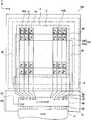
도 1은 본 발명의 실시예 1에 따른 액정 장치(100)의 개략 구성을 모식적으로 나타내는 평면도이다. 도 1에서는, 지면측 전방(관찰측)에 컬러 필터 기판(92)이 배치되어 있는 한편, 지면 깊이측에 소자 기판(91)이 배치되어 있다. 또, 도 1에서는, 지면 종방향(열방향)을 Y 방향으로, 또한, 지면 횡방향(행방향)을 X 방향으로 규정한다. 또한, 도 1에 있어서, R, G, B의 각 색에 대응하는 영역은 하나의 서브 화소 영역(SG)을 표시하고, 또한, R, G, B의 각 색의 서브 화소 영역 SG에 의해 구성되는 1행 3열의 화소 배열은, 하나의 화소 영역 AG을 나타내고 있다. 또, 이하에서는, 하나의 서브 화소 영역 SG 내에 존재하는 하나의 표시 영역을 「서브 화소」라고 하며, 또한, 하나의 화소 영역 AG 내에 대응하는 표시 영역을 「1 화소」라고 하는 것도 있다.1 is a plan view schematically showing a schematic configuration of a
액정 장치(100)는, 소자 기판(91)과, 그 소자 기판(91)에 대향하여 배치되는 컬러 필터 기판(92)이 프레임 형상의 밀봉재(5)를 거쳐서 접합되고, 그 밀봉재(5) 의 내측에 액정이 봉입되어 액정층(4)이 형성되어 이루어진다.In the
여기에, 액정 장치(100)는, R, G, B의 3색을 이용하여 구성되는 컬러 표시용의 액정 장치이며, 또한, 스위칭 소자로서 LTPS(저온 폴리실리콘)형의 TFT 소자(이하, 「LTPS형 TFT 소자(21)」라고 한다)를 이용한 액티브 매트릭스 구동 방식의 액정 장치이다. 또한, 이 액정 장치(100)는, 화소 전극 등의 각종 전극이 형성된 소자 기판(91) 측에서, 해당 소자 기판(91) 면에 대략 평행한 방향, 및 대략 수직인 방향(관찰측)으로 프린지 필드(전계 E)를 발생시켜 액정 분자의 배향을 제어하는, 이른바 FFS 방식의 액정 장치이다. 이 때문에, 이 액정 장치(1OO)에서는 높은 시야각 등을 얻을 수 있다. 또한, 액정 장치(100)는, 투과형 표시만을 행하는 투과형의 액정 장치이다.Here, the
우선, 소자 기판(91)의 평면 구성에 대하여 설명한다. 소자 기판(91)의 내면상에는, 주로, 복수의 소스선(32), 복수의 게이트선(33), 복수의 LTPS형 TFT 소자(21), 복수의 화소 전극(10), 공통 전극(20), 드라이버 IC(40), 외부 접속용 배선(35) 및 FPC(Flexible Printed Circuit)(41) 등이 형성 또는 실장되어 있다.First, the planar structure of the
도 1에 도시하는 바와 같이, 소자 기판(91)은, 컬러 필터 기판(92)의 1 근처측에서 외측으로 돌출하는 돌출 영역(36)을 갖고 있고, 그 돌출 영역(36) 상에는, 드라이버 IC(40)가 실장되어 있다. 드라이버 IC(40)의 입력측의 단자(도시 생략)은, 복수의 외부 접속용 배선(35)의 한쪽 단부측과 전기적으로 접속되어 있고, 또한, 복수의 외부 접속용 배선(35)의 다른 쪽 단부측은 FPC(41)와 전기적으로 접속되어 있다.As shown in FIG. 1, the
각 소스선(32)은, Y 방향으로 연재하면서, X 방향으로 적절한 간격을 두고 형성되어 있고, 각 소스선(32)의 한쪽 단부측은, 드라이버 IC(40)의 출력측의 단자(도시 생략)에 전기적으로 접속되어 있다.Each
각 게이트선(33)은, 예컨대, Ti(티탄)/Al(알루미늄)/Ti(티탄)의 3층 구조를 갖고, Y 방향으로 연재하도록 형성된 제 1 배선(33a)과, 그 제 1 배선(33a)의 종단부로부터 X 방향으로, 또한 후술하는 유효 표시 영역(V) 내에 연재하도록 형성된 제 2 배선(33b)을 구비하고 있다. 각 게이트선(33)의 제 2 배선(33b)은, 각 소스선(32)과 교차하는 방향, 즉 X 방향으로 연재하도록, 또한 Y 방향으로 적절한 간격을 두고 형성되어 있고, 각 게이트선(33)의 제 1 배선(33a)의 한쪽 단부측은, 드라이버 IC(40)의 출력측의 단자(도시 생략)에 전기적으로 접속되어 있다.Each
각 소스선(32)과 각 게이트선(33)의 제 2 배선(33b)의 교차 위치 부근에는 LTPS형 TFT 소자(21)가 대응하여 마련되어 있고, LTPS형 TFT 소자(21)는 각 소스선(32), 각 게이트선(33) 및 각 화소 전극(10) 등에 전기적으로 접속되어 있다.The LTPS
각 화소 전극(10)는, 예컨대 ITO 등의 투명 도전 재료에 의해 형성되어, 각 서브 화소 영역 SG 내에 대응하여 설치된다.Each
공통 전극(20)은, 화소 전극(10)과 동일한 재료에 의해 형성되어, 유효 표시 영역 V와 대략 동일한 크기의 영역(파선으로 둘러싸인 영역)을 갖고, 도 2에 나타내는 제 3 절연막(유전막)(53)을 거쳐서 각 화소 전극(10)의 하측에 대략 베타 형상으로 마련된다. 공통 전극(20)은, 해당 공통 전극(20)과 동일한 재료 등으로 이루어지는 배선(27)을 통하여, 드라이버 IC(40)의 COM 단자와 전기적으로 접속되어 있다.The
하나의 화소 영역 AG이 X 방향 및 Y 방향으로 복수개, 매트릭스 형상으로 한줄로 세워진 영역이 유효 표시 영역 V(2점 쇄선에 의해 둘러싸이는 영역)이다. 이 유효 표시 영역 V에, 문자, 숫자, 도형 등의 화상이 표시된다. 또, 유효 표시 영역 V의 외측 영역은 표시에 기여하지 않는 프레임 영역(38)으로 되어 있다. 또한, 각 화소 전극(10) 등의 내면상에는, 도시하지 않는 배향막이 형성되어 있다. 이러한 배향막은, 소정의 방향으로 러빙 처리(도 2를 참조)가 실시되고 있다.An area in which one pixel area AG is arranged in a plurality of rows in the X and Y directions and in a matrix form is an effective display area V (area surrounded by a dashed-dotted line). In this effective display area V, images such as letters, numbers and graphics are displayed. The outer region of the effective display region V is the
다음에, 컬러 필터 기판(92)의 평면 구성에 대하여 설명한다. 컬러 필터 기판(92)은, 차광층(일반적으로 「블랙 매트릭스」라고 하고, 이하에서는, 단지 「BM」으로 약기), R, G, B의 3색의 착색층(6R, 6G, 6B), 오버코팅층(16)(도 3을 참조)및 배향막(18)(도 3을 참조) 등을 갖는다. 또, 이하의 설명에 있어서, 색을 묻지않고서 착색층을 가리키는 경우는 단지 「착색층(6)」이라 표기하고, 색을 구별하여 착색층을 가리키는 경우는 「착색층(6R)」 등으로 표기한다. BM은, 각 서브 화소 영역 SG을 구획하는 위치 등에 형성되어 있다.Next, the planar structure of the
이상의 구성을 갖는 액정 장치(100)에서는, 전자기기 등과 접속된 FPC(41)측으로부터의 신호 및 전력 등에 근거하여, 드라이버 IC(40)에 의해서, G1, G2,..., Gm-1, Gm(m : 자연수)의 순서대로 게이트선(33)이 순차 배타적으로 1개씩 선택되고, 또한, 선택된 게이트선(33)에는, 선택 전압의 게이트 신호가 공급되는 한편, 다른 비선택의 게이트선(33)에는, 비선택 전압의 게이트 신호가 공급된다. 그리고, 드라이버 IC(40)는, 선택된 게이트선(33)에 대응하는 위치에 존재하는 화소 전 극(10)에 대하여, 표시 내용에 따른 소스 신호를, 각각 대응하는 S1, S2,..., Sn-1, Sn(n : 자연수)의 소스선(32) 및 각 LTPS형 TFT 소자(21)를 거쳐서 공급한다. 그 결과, 액정층(4)의 표시 상태가, 비표시 상태 또는 중간 표시 상태로 전환되어, 액정층(4) 내의 액정 분자의 배향 상태가 제어되는 것으로 된다. 이것에 의해, 유효 표시 영역 V 내에서 소망하는 화상을 표시할 수 있다.In the
(화소 구성)(Pixel configuration)
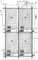
다음에, 도 2 및 도 3을 참조하여, 본 발명의 실시예 1에 따른 액정 장치(100)의 화소 구성 등에 대하여 설명한다.Next, with reference to FIGS. 2 and 3, the pixel configuration of the
도 2는, 실시예 1에 따른 소자 기판(91)에 배치될 수 있는 4 화소 분의 평면 구성을 나타낸다. 도 3은, 도 2에 있어서의 절단선 A-A'에 따른 단면도를 나타내고, 또한, LTPS형 TFT 소자(21)를 지나는 위치로 절단했을 때의 1 서브 화소의 단면 구성을 나타낸다.FIG. 2 shows a planar configuration of four pixels that can be disposed on the
우선, 도 2 및 도 3을 참조하여, 실시예 1의 소자 기판(91)에 있어서의 화소 구성 등에 대하여 설명한다.First, referring to Figs. 2 and 3, the pixel configuration and the like in the
하측 기판(1)의 내면상에는, 소스선(32)과 게이트선(33)의 제 2 배선(33b)의 교차 위치에 대응하여 대략 コ의 글자 형상의 평면 형상을 갖는 저온형의 P-Si(폴리실리콘)층(19)이 형성되어 있다. P-Si 층(19) 및 하측 기판(1)의 내면상에는, 그 대략 일면에 걸쳐, 예컨대 SiO2등으로 이루어지는 게이트 절연막(50)이 형성되 어 있다.On the inner surface of the
게이트 절연막(50)은, P-Si 층(19)의 한쪽 단부측에 또한 소스선(32)의 일부와 평면적으로 겹치는 위치에 제 1 콘택트 홀(50a)을 갖고, 또한, P-Si 층(19)의 다른쪽 단부측에 대응하는 위치에 제 2 콘택트 홀(50b)을 갖는다. 게이트 절연막(50)의 내면상에는 게이트선(33)이 형성되어 있고, 그 게이트선(33)의 제 2 배선(33b)은, 도 2에 도시하는 바와 같이, Y 방향으로 일정한 간격을 두고 X 방향으로 연재하도록 형성되고, 해당 제 2 배선(33b)은, P-Si 층(19)과 부분적 또한 평면적으로 겹치고 있다.The
게이트선(33) 및 게이트 절연막(50)의 내면상에는, 예컨대 SiO2등으로 이루어지는 제 1 절연막(51)이 형성되어 있다. 제 1 절연막(51)은, 제 1 콘택트 홀(50a)에 대응하는 위치에 제 1 콘택트 홀(51a)을 갖고, 또한, 제 2 콘택트 홀(50b)에 대응하는 위치에 제 2 콘택트 홀(51b)을 갖는다. 제 1 절연막(51)의 내면상에는, 소스선(32) 및 중계 전극(77)이 설치된다.On the inner surfaces of the
소스선(32)은, 도 2에 도시하는 바와 같이 X 방향에 일정한 간격을 두고 Y 방향으로 연재하도록 형성되어 있다. 소스선(32)의 일부는, P-Si 층(19)의 한쪽 단부측의 일부와 평면적으로 중첩된다. 소스선(32)의 일부는, 제 1 콘택트 홀(50a 및 51a) 내까지 들어가도록 마련되어 있고, 해당 소스선(32)은, P-Si 층(19)의 한쪽 단부측과 전기적으로 접속되어 있다. 중계 전극(77)은, P-Si 층(19)의 다른쪽 단부측의 일부와 평면적으로 중첩된다. 중계 전극(77)의 일부는, 제 2 콘택트 홀(50b 및 51b) 내까지 들어가도록 마련되어 있고, 해당 중계 전극(77)은, P-Si 층(19)의 다른쪽 단부측과 전기적으로 접속되어 있다. 이것에 의해, 각 소스선(32)은, 대응하는 각 P-Si 층(19)을 거쳐서, 대응하는 각 중계 전극(77)에 전기적으로 접속되어 있다. 이렇게 해서, 각 P-Si 층(19)에 대응하는 위치에 또한 소스선(32)과 게이트선(33)의 제 2 배선(33b)과의 교차 위치에 대응하여 LTPS형 TFT 소자(21)가 설치된다.As shown in FIG. 2, the
소스선(32), 중계 전극(77) 및 제 1 절연막(51)의 내면상에는, 예컨대 아크릴수지 등으로 이루어지는 제 2 절연막(52)이 형성되어 있다. 제 2 절연막(52)의 내면상은 평탄성을 갖고, 제 2 절연막(52)은 평탄화막을 구성하고 있다. 제 2 절연막(52)은, 중계 전극(77)의 한쪽 단부측에 또한 제 2 콘택트 홀(50b 및 51b)의 근방 위치에 콘택트 홀(52a)을 갖는다. 또, 본 발명에서는, 제 1 절연막(51)과 제 2 절연막(52) 사이에, 예컨대 SiNx 등으로 이루어진 절연막을 더 마련하도록 하더라도 상관없다.On the inner surfaces of the
제 2 절연막(52)의 내면상에는, 그 대략 일면에 걸쳐, COM 단자에 접속된 공통 전극(20)이 형성되어 있다(도 1 참조). 공통 전극(20)은, 예컨대 ITO 등의 투명 재료에 의해 형성되어, 콘택트 홀(52a)에 대응하는 위치에 개구(20a)를 갖는다. 콘택트 홀(52a) 내에 위치하는 제 2 절연막(52)의 일부, 및 공통 전극(20)의 내면상에는, 예컨대 SiO2나 SiNx 등으로 이루어지는 제 3 절연막(53)이 형성되어 있다. 제 3 절연막(53)은, 제 2 절연막(52)의 콘택트 홀(52a)에 대응하는 위치에 콘택트 홀(53a)을 갖는다. 제 3 절연막(53)은, 공통 전극(20)과 후술하는 화소 전극(10) 사이에 마련되기 때문에, 보조 용량을 형성하는 유전막으로서 기능한다. 여기서, 충분한 보조 용량을 확보하기 위해서는, 제 3 절연막(53)의 두께 d1는, 가능한 한 얇게 설정되어 있는 것이 바람직하다.On the inner surface of the second insulating
이러한 목적을 실현하기 위해서, 바람직한 예에서는, 제 3 절연막(53)의 두께 d1은, 자신에게 형성되는 보조 용량의 크기가 약 100 ~ 60O fF, 보다 바람직하게는 약 200 ~ 80O fF로 설정하도록 결정하는 것이 바람직하다. 또한, 선명도 200 PPi 이상에서는, 제 3 절연막(53)의 두께 d1는 대략 50 ~ 400 ㎚로 설정하는 것이 바람직한 한편, 선명도 200 PPi 미만에서는, 제 3 절연막(53)의 두께 d1은 대략 200 ~ 1000 ㎚로 설정하는 것이 좋다.In order to realize this object, in a preferred example, the thickness d1 of the third insulating
제 3 절연막(53)의 내면상에 있어서, 각 서브 화소 영역 SG 내에는, 예컨대 ITO 등의 투명 도전 재료로 이루어지는 화소 전극(10)이 형성되어 있다. 화소 전극(10)은, 콘택트 홀(52a)을 거쳐서 중계 전극(77)과 전기적으로 접속되어 있다. 이 때문에, 소스선(32)으로부터의 소스 신호는, LTPS형 TFT 소자(21) 및 중계 전극(77)을 거쳐서 화소 전극(10)에 공급된다. 또한, 화소 전극(10)은, 제 3 절연막(53)을 거쳐서 공통 전극(20)과 대향하여 또한 평면적으로 겹치고 있다. 화소 전극(10)에는, 자신과 공통 전극(20) 사이에서, 프린지 필드(전계 E)를 발생시키기 위한 복수의 슬릿(1Oa)이 설치된다. 각 슬릿(10a)은, 도 2에 있어서, 소스선(32)의 연재 방향으로 일정한 간격을 두고, 또한 게이트선(33)의 제 2 배선(33b)의 연재 방향에 대하여 시계 회전 방향으로 소정 각도만큼 회전시킨 방향으로 연재하도 록 설치된다.On the inner surface of the third insulating
제 3 절연막(53)의 일부, 및 화소 전극(10)의 내면상에는 도시하지 않은 배향막이 형성되어 있다. 이러한 배향막에는, 도 2에 도시하는 바와 같이, 게이트선(33)의 제 2 배선(33b)의 연재 방향인 X 방향을 기준으로 반시계 회전 방향으로 각도 θ, 바람직하게는 약 5°의 방향(이하, 「러빙 방향 R」이라 부른다)에 러빙 처리가 실시되고 있다. 이 때문에, 액정 분자(4a)는, 초기 배향 상태에 있어서, 그 길이축 방향이 러빙 방향 R에 따른 상태로 배향하고 있다. 또한, 하측 기판(1)의 하측에는 편광판(11)이 설치되고, 또한, 편광판(11)의 하측에는 조명 장치로서의 백라이트(15)가 설치된다. 이렇게 해서, 실시예 1에 따른 화소 구성을 포함하는 소자 기판(91)이 구성되어 있다.An alignment film (not shown) is formed on a part of the third insulating
한편, 상기의 화소 구성에 대응하는 컬러 필터 기판(92)의 구성은 다음과 같다.In addition, the structure of the color filter board |
상측 기판(2)의 내면상에 있어서, 각 서브 화소 영역 SG 내에는 적색의 착색층(6R), 녹색의 착색층(6G) 및 청색의 착색층(6B) 중 어느 하나로 이루어지는 착색층(6)이 설치된다. 상측 기판(2)의 내면상에 있어서, 각 서브 화소 영역 SG을 구획하는 위치 및 LTPS형 TFT 소자(21)에 대응하는 위치에는 BM이 설치된다. 이 때문에, LTPS형 TFT 소자(21), 소스선(32) 및 게이트선(33)의 제 2 배선(33b) 등은 BM과 평면적으로 겹치고 있다. BM 및 각 착색층(6)의 내면상에는 오버코팅층(16)이 형성되어 있다. 이 오버코팅층(16)은, 액정 장치(100)의 제조 공정중에 사용되는 약제 등에 의한 부식이나 오염으로부터, 착색층(6) 등을 보호하는 기능을 갖고 있다. 오버코팅층(16)의 내면상에는 소정의 방향으로 러빙 처리가 실시된 배향막(18)이 형성되어 있다. 이렇게 해서, 실시예 1에 따른 컬러 필터 기판(92)이 구성되어 있다.On the inner surface of the
이상의 구성을 갖는 액정 장치(100)에서는, 그 구동시, 도 2에 도시하는 바와 같이 러빙 방향 R에 따라 초기 배향 상태에 있는 액정 분자(4a)는, 소스선(32)의 연재 방향으로 발생하는 프린지 필드(전계 E)에 의해서 반시계 회전 방향으로 회전하여 소스선(32)의 연재 방향으로 재배향한다. 또, 도 3의 단면 구성에서는, 프린지 필드(전계 E)는, 소자 기판(91)과 대략 평행한 방향(도 3의 지면 횡방향) 및 대략 수직인 방향(도 3의 컬러 필터 기판측)에 강한 전계 성분을 갖고, 화소 전극(10)과, 그 복수의 슬릿(10a) 및 제 3 절연막(53)을 거쳐서 공통 전극(20)과의 사이에서 발생한다. 이것에 의해, 액정 분자(4a)의 배향 상태가 제어되어, 투과형 표시를 행할 수 있다. 구체적으로는, 이 투과형 표시시에, 백라이트(15)로부터 출사한 조명광은, 도 3에 나타내는 경로 T에 따라 진행하고, 공통 전극(20), 화소 전극(10) 및 R, G, B의 각 착색층(6) 등을 통과하여 관찰자에게 도달한다. 이 경우, 그 조명광은, 그 착색층(6) 등을 투과함으로써 소정의 색상 및 밝기를 나타낸다. 이렇게 해서, 소망하는 컬러 표시 화상이 관찰자에 의해 시인된다.In the
다음에, 비교예와 비교한 실시예 1에 따른 액정 장치(100)의 특유의 작용 효과에 대하여 설명한다.Next, the specific effects of the
우선, 도 4 및 도 5를 참조하여, 비교예에 따른 FFS 방식의 액정 장치(500)의 구성에 대하여 설명한다. 또, 비교예에 있어서, 실시예 1과 공통하는 요소에 대해서는 동일한 부호를 부여하여, 그 설명은 간략화 또는 생략한다.First, with reference to FIG. 4 and FIG. 5, the structure of the FFS system
도 4는, 도 2에 대응하는 비교예에 따른 소자 기판(93)에 있어서의 4 화소분의 평면 구성을 나타낸다. 도 5는, 도 4에 있어서의 절단선 B-B'에 따른 단면도를 나타내고, 또한, α-Si 형 TFT 소자(23)를 지나는 위치로 절단했을 때의 1 서브 화소의 단면 구성을 나타낸다.FIG. 4 shows a planar configuration of four pixels in the
비교예에 따른 액정 장치(500)는, α-Si 형 TFT 소자(23)를 갖는 소자 기판(93)과, 컬러 필터 기판(92)과의 사이에 액정이 봉입되어 액정층(4)이 형성되어 이루어진다.In the
우선, 소자 기판(93)의 구성은 다음과 같다.First, the structure of the
하측 기판(1) 상에는, 서브 화소 영역 SG 마다 ITO 등으로 이루어지는 공통 전극(20)(2점 쇄선으로 둘러싸인 영역)이 설치된다. 공통 전극(20)의 일부 위 및 하측 기판(1) 상에는, 도 4에 나타내는 바와 같이, Y 방향으로 일정한 간격을 두고 형성되고, X 방향으로 연재하는 공통 전극선(20x)이 설치된다. 이 때문에, 공통 전극(20)은, 공통 전극선(20x)에 전기적으로 접속되어 있다. 공통 전극선(20x)은, 도시를 생략하지만, 소자 기판(93) 상의 소정 위치에 있어서 COM용 단자와 전기적으로 접속되어 있다. 하측 기판(1) 상에는, Y 방향으로 일정한 간격을 두고 X 방향으로 연재하도록 게이트선(33)의 제 2 배선(33b)이 설치된다. 제 2 배선(33b)은, 인접하는 화소에 대응하여 마련된 공통 전극선(20x)의 근방 위치에 설치된다.On the lower board |
공통 전극(20), 공통 전극선(20x), 게이트선(33) 및 하측 기판(1)의 위에는, 게이트 절연막(50)이 형성되어 있다. 게이트 절연막(50) 상에 있어서, 후술하는 소스선(32)과, 게이트선(33)의 제 2 배선(33b)과의 교차 위치 근방에는, α-Si 형 TFT 소자(23)의 요소로 되는 α-Si 층(26)이 설치된다.The
도 4에 있어서, 게이트 절연막(50)상에는, Y 방향으로 연재하도록 소스선(32)이 설치된다. 소스선(32)은, α-Si 층(26)상에 겹치도록 절곡되고, 해당 α-Si 층(26)과 전기적으로 접속되는 절곡 부분(32x)을 갖는다. 또한, α-Si 층(26) 및 게이트 절연막(50)상에는, 드레인 전극(34)이 설치된다. 이 때문에, 드레인 전극(34)은, α-Si 층(26)과 전기적으로 접속되어 있다. 이 때문에, 소스선(32)의 절곡 부분(32x)은, α-Si 층(26)을 거쳐서 드레인 전극(34)에 전기적으로 접속되어 있다. 이렇게 해서, 그 영역에는α-Si 형 TFT 소자(23)가 형성되어 있다.In FIG. 4, the
게이트 절연막(50) 및α-Si 형 TFT 소자(23) 상에는, 예컨대 SiNx 등으로 이루어지는 패시베이션층(54)이 형성되어 있다. 패시베이션층(54)은, 공통 전극(20)의 일부와 겹치는 위치에 또한 드레인 전극(34)의 한쪽 단부측과 겹치는 위치에 콘택트 홀(54a)을 갖는다.On the
패시베이션층(54)상에는, 서브 화소 영역 SG 마다 ITO 등으로 이루어지는 화소 전극(10)이 형성되어 있다. 화소 전극(10)의 구성은 실시예 1과 마찬가지다. 즉, 화소 전극(10)은, 복수의 슬릿(10a)을 갖고, 콘택트 홀(54a)을 통하여 드레인 전극(34)에 전기적으로 접속되어 있다. 이 때문에, 화소 전극(10)에는, 소스선(32)으로부터의 소스 신호가 α-Si 형 TFT 소자(23)를 거쳐서 공급된다. 화소 전극(10) 등의 위에는 도시하지 않는 배향막이 형성되어 있다. 이러한 배향막에는, 실시예 1과 동일한 방향으로 러빙 처리가 실시되어 있다.On the
이상의 구성을 갖는 비교예에 따른 액정 장치(500)에서는, 그 구동시, 실시예 1에 따른 액정 장치(100)와 동일한 원리에 의해 액정의 배향이 제어되어, 투과형 표시가 이루어진다.In the
이러한 구성을 갖는 비교예에서는, 다음과 같은 과제를 갖고 있다.In the comparative example which has such a structure, it has the following subjects.
즉, 비교예에 따른 α-Si 형 TFT 소자(23)를 갖는 액정 장치(500)에서는, 도 5에 도시하는 바와 같이, 실시예 1에 상당하는 평탄화막(제 2 절연막(52))이 설치되지 않는다. 이 때문에, 특히, 공통 전극선(20x)의 일부와 평면적으로 겹치는 영역 A1, 및, α-Si 형 TFT 소자(23)의 요소인 드레인 전극(34)의 일부와 평면적으로 겹치는 영역 A2, 및, 소스선(32)의 일부와 평면적으로 겹치는 영역 A3에서는, 화소 전극(10)의 부분은 요철 형상의 형상(단차 형상)으로 형성되어 있다. 이러한 단차 형상을 갖는 화소 전극(10)의 부분으로서는 액정 분자(4a)의 배향 흐트러짐이 발생하여, 표시 품질에 악영향을 주기 때문에, 그 화소 전극(10)의 부분을 표시 영역으로서 이용할 수 없다. 따라서, 일반적으로는, 컬러 필터 기판(92)에 있어서, 그 화소 전극(10)의 부분에 대응하는 위치에는, 그와 같은 액정 분자(4a)의 배향 흐트러짐에 의한 표시 품질의 열화를 덮어서 숨기기 위한 BM이 마련된다. 이것에 의해, 비교예에서는 개구율이 저하해 버린다고 하는 문제가 있다. 더구나, 비교예에서는, 공통 전극(20)의 그 외에 공통 전극선(20x)을 더 마련하도록 하고 있기 때문에, 점점 개구율이 저하해 버린다고 하는 문제가 있다.That is, in the
또한, 비교예에서는, 화소 전극(10)과 공통 전극(20) 사이에 마련된 유전막으로서의 패시베이션층(54) 및 게이트 절연막(50)의 사이에는 보조 용량이 형성되 지만, 상술한 바와 같이, 개구율이 저하함에 따라, 화소 전극(10)과 공통 전극(20)과의 평면적으로 겹치는 면적이 작아지고, 소망하는 보조 용량을 얻을 수 없게 되는 우려가 있다. 이상, 비교예의 유전막의 두께 d2는, 실시예 1와 비교해서 상당히 두껍기 때문에, 일반적인 정전 용량의 식에 근거하여 보조 용량의 크기는 점점 작아진다. 이 때문에, 이러한 구성을 갖는 비교예는, 고선명용의 액정 표시 장치에는 적용하기 어렵다고 하는 문제가 있다.In the comparative example, an auxiliary capacitance is formed between the
이 점, 실시예 1에 따른 액정 장치(100)에서는, 소자 기판(91) 측에서, 평탄성을 갖는 제 2 절연막(평탄화막)(52)이, 화소 전극(10), 제 3 절연막(53) 및 공통 전극(20)의 하측에 설치된다. 이것에 의해, 적어도 소스선(32) 및 LTPS형 TFT 소자(21)에 위치하는 화소 전극(10), 제 3 절연막(53) 및 공통 전극(20)을 평탄화할 수 있다. 즉, 서브 화소 영역 SG 내에는 요철 형상의 형상(단차 형상)을 갖는 전극 부분이 형성되지 않는다. 이것에 의해, 소스선(32) 및 LTPS형 TFT 소자(21)부근에서 액정 분자(4a)의 배향 흐트러짐이 발생하는 것을 방지할 수 있는 결과, 화소 전극(10)을, 소스선(32) 및 LTPS형 TFT 소자(21)부근뿐만 아니라, 인접하는 다른 화소 전극(10) 부근까지 연재시킬 수 있다. 따라서, 비교예와 비교해서 고개구율을 실현할 수 있다.In this regard, in the
또한, 실시예 1에서는, 공통 전극(20)을, 제 2 절연막(평탄화막)(52) 상에 그 대략 일면에 걸친 형상으로 배치(단지, 콘택트 홀(52a)의 부분은 제외한다)하고 있기 때문에 공통 전극(20)에 대한 시정수(콘덴서 C와 저항 R의 곱)를 작은 값으로 할 수 있다. 따라서, 실시예 1에서는, 비교예에 상당하는 공통 전극선(20x)을 마 련하고 있지 않다. 이 점으로부터도 화소 전극(10) 등의 유효 면적을 크게 할 수 있어, 고개구율을 실현할 수 있다.In addition, in Example 1, the
이것에 의해, 고선명용의 액정 표시 장치에 적합하게 이용하는 것이 가능해진다.Thereby, it becomes possible to use suitably for the liquid crystal display device for high definition.
또한, 실시예 1에서는, 유전막으로서의 제 3 절연막(53)을 화소 전극(10)과 공통 전극(20) 사이에 마련하고 있기 때문에, 제 3 절연막(53)의 두께를 조정하기 쉽게 되어, 비교예와 비교해서 보조 용량의 크기의 조정이 용이해 진다. 예컨대, 고선명용의 액정 표시 장치 등 보조 용량을 크게 할 필요가 있는 경우에, 제 3 절연막(53)의 두께 d1을 얇게 설정하는 것으로 필요 충분한 보조 용량을 얻을 수 있다. 따라서, 표시 품질의 향상, 또한 저소비 전력화를 도모할 수 있다.In addition, in Example 1, since the 3rd insulating
바람직한 예로서는, 제 3 절연막(53)의 두께 d1은, 자신에게 형성되는 보조 용량의 크기가 대략 100 ~ 60O fF, 보다 바람직하게는 대략 200 ~ 80O fF로 설정하 도록 결정하는 것이 바람직하다. 또한, 선명도 200 PPi 이상에서는, 제 3 절연막(53)의 두께 d1은 대략 50 ~ 400 ㎚로 설정하는 것이 바람직한 한편, 선명도 200 PPi 미만에서는, 제 3 절연막(53)의 두께 d1는 약 200 ~ 1000 ㎚로 설정하는 것이 바람직하다.As a preferable example, the thickness d1 of the third insulating
또한, 유전막으로서의 제 3 절연막(53)의 두께 d1을 얇게 설정할 수 있음에 따라, 화소 전극(10)과 공통 전극(20) 사이에 형성되는 프린지 필드(전계 E)도 강하게 되어, 보다 저전압이더라도 액정 분자(4a)를 용이하게 동작시키는 것이 가능해진다. 예컨대, 노멀리 블랙의 표시 모드에 있어서 제 3 절연막(53)의 두께 d1를 약 50 ~ 200 ㎚로 설정한 경우에는, 화소 전극(10)과 공통 전극(20) 사이에 인가되는 백표시에 대응하는 구동 전압은 약 2 ~ 5 V 정도로 할 수 있다. 또한, 노멀리 블랙의 표시 모드에 있어서 제 3 절연막(53)의 두께 d1을 약 200 ~ 600 ㎚로 설정한 경우에는, 화소 전극(10)과 공통 전극(20) 사이에 인가되는 백표시에 대응하는 구동 전압은 약 3 ~ 5 V 정도로 할 수 있다. 또한, 제 3 절연막(53)의 두께 d1은 지극히 얇게 설정되기 때문에, 제 3 절연막(53)의 형성에 있어서, 처리량(throughput)의 향상을 도모할 수 있다.In addition, since the thickness d1 of the third insulating
또한, 실시예 1로서는, 컬러 필터 기판(92) 측에서, 상기 각 콘택트 홀에 대응하는 위치에 BM을 배치하고 있기 때문에, 해당 각 콘택트 홀의 부근에서 액정 분자(4a)의 배향 흐트러짐이 발생한 경우에도, 그 배향 흐트러짐의 영역을 BM에 의해서 덮어서 숨길 수 있다. 따라서, 액정 분자(4a)의 배향 흐트러짐에 따라 표시 품질이 저하하는 것을 방지할 수 있다.In addition, in Example 1, since BM is arrange | positioned in the position corresponding to each said contact hole in the color filter board |
(실시예 2)(Example 2)
다음에, 도 6 및 도 7을 참조하여, 본 발명의 실시예 2에 따른 액정 장치(200)의 구성에 관하여 설명한다. 여기서, 실시예 2에 따른 액정 장치(200)는, LTPS형 TFT 소자(21)를 갖는 FFS 방식의 액정 장치이며, 또한, 투과형의 액정 장치이다. 또, 이하에서는, 실시예 1과 동일한 요소에 관하여는 동일한 부호를 부여하여, 그 설명은 간략화 또는 생략한다.Next, with reference to FIG. 6 and FIG. 7, the structure of the
도 6은, 실시예 2에 따른 소자 기판(93)에 있어서의 4 화소분의 평면 구성을 나타낸다. 도 7은, 도 6에 있어서의 절단선 C-C'에 따른 단면도를 나타내고, 또한, LTPS형 TFT 소자(21)를 지나는 위치로 절단했을 때의 1서브 화소의 단면 구성을 나타낸다.6 shows a planar configuration of four pixels in the
우선, 도 6 및 도 7을 참조하여, 실시예 2의 소자 기판(93)에 있어서의 화소 구성 등에 대하여 설명한다.First, with reference to FIG. 6 and FIG. 7, the pixel structure etc. in the
하측 기판(1)의 내면상에 있어서, 소스선(32)과 게이트선(33)의 제 2 배선(33b)의 교차 위치에는 P-Si 층(19)이 형성되어 있다. P-Si 층(19) 및 하측 기판(1)의 내면상에는, 그 대략 일면에 걸쳐, 제 1 콘택트 홀(50a) 및 제 2 콘택트 홀(50b)을 갖는 게이트 절연막(50)이 형성되어 있다. 또, 제 1 콘택트 홀(50a) 및 제 2 콘택트 홀(50b)의 형성 위치는 실시예 1과 마찬가지다.On the inner surface of the
게이트 절연막(50)의 내면상에는, 도 6에 도시하는 바와 같이 게이트선(33)의 제 2 배선(33b)이 Y 방향으로 일정한 간격을 두고 X 방향으로 연재하도록 형성되고, 해당 제 2 배선(33b)의 일부는, P-Si 층(19)과 평면적으로 겹치는 위치에 마련된다. 게이트 절연막(50)의 내면상에 있어서, 게이트선(33)의 제 2 배선(33b)에 인접하는 위치에는, 해당 제 2 배선(33b)의 연재 방향과 같은 방향으로 연재하도록 공통 전극선(20x)이 형성되어 있다. 공통 전극선(20x)은, 상술한 게이트선(33)과 동일한 재료에 의해 형성되어 있는 것이 바람직하다. 공통 전극선(20x)은, 드라이버 IC(40) 내에 마련된 COM 단자와 전기적으로 접속되어 있다.On the inner surface of the
공통 전극선(20x), 게이트선(33) 및 게이트 절연막(50)의 내면상에는, 제 1 콘택트 홀(51a) 및 제 2 콘택트 홀(51b)을 갖는 제 1 절연막(51)이 형성되어 있다. 제 1 콘택트 홀(51a) 및 제 2 콘택트 홀(51b)의 형성 위치는 실시예 1과 마찬가지다. 제 1 절연막(51)은, 또한, P-Si 층(19)의 근방 위치에 또한 공통 전극선(20x)에 대응하는 위치에 제 3 콘택트 홀(51c)을 갖는다.On the inner surfaces of the
도 6에 있어서, 제 1 절연막(51)의 내면상에는, 서로 인접하는 서브 화소 영역 SG의 사이에 Y 방향으로 연재하도록 소스선(32)이 설치된다. 소스선(32)의 일부는, 제 1 콘택트 홀(50a 및 51 a)을 거쳐서, P-Si 층(19)의 한쪽 단부측에 전기적으로 접속되어 있다. 제 1 절연막(51)의 내면상에 있어서, P-Si 층(19)의 다른 쪽 단부측과 평면적으로 겹치는 위치에는 중계 전극(77)이 설치된다. 제 1 절연막(51)의 내면상에 있어서, 제 3 콘택트 홀(51c)과 평면적으로 겹치는 위치 및 공통 전극선(20x)과 게이트선(33)의 제 2 배선(33b) 사이에 대응하는 위치에는 다른 중계 전극(34)이 설치된다.In Fig. 6, on the inner surface of the first insulating
중계 전극(77)은, 제 2 콘택트 홀(50b 및 51b)을 거쳐서 P-Si 층(19)의 다른쪽 단부측에 전기적으로 접속되어 있다. 이 때문에, 소스선(32)은, P-Si 층(19)을 거쳐서 중계 전극(77)에 전기적으로 접속되어 있다. 이것에 의해, P-Si 층(19)에 대응하는 위치에 또한 소스선(32)과 게이트선(33)의 제 2 배선(33b)과의 교차 위치에는 LTPS형 TFT 소자(21)가 형성되어 있다. 한편, 다른 중계 전극(34)은, 제 3 콘택트 홀(51c)을 거쳐서 공통 전극선(20x)에 전기적으로 접속되어 있다.The
소스선(32), 중계 전극(77), 다른 중계 전극(34) 및 제 1 절연막(51)의 내면상에는, 콘택트 홀(52a)을 갖고, 평탄화막인 제 2 절연막(52)이 형성되어 있다. 또, 콘택트 홀(52a)의 형성 위치는 실시예 1과 마찬가지다. 제 2 절연막(52)의 내 면상에는, 서브 화소 영역 SG 마다 화소 전극(10)이 형성되어 있다. 화소 전극(10)은, 콘택트 홀(52a)을 거쳐서 중계 전극(77)과 전기적으로 접속되어 있다. 이 때문에, 화소 전극(10)에는, 소스선(32)으로부터의 소스 신호가 LTPS형 TFT 소자(21) 및 중계 전극(77)을 거쳐서 공급된다.On the inner surface of the
화소 전극(10) 및 제 2 절연막(52)의 내면상에는, 콘택트 홀(53a)을 갖고, 유전막인 제 3 절연막(53)이 형성되어 있다. 또, 콘택트 홀(53a)의 형성 위치는 실시예 1과 마찬가지다. 제 3 절연막(53)의 내면상에는, 공통 전극(20)이 설치된다. 이 때문에, 각 공통 전극(20)은, 제 3 절연막(53)을 거쳐서 각 화소 전극(10)에 대향하여 또한 평면적으로 겹치고 있다. 또한, 본 예에서는, 각 서브 화소에 대응하는 각 공통 전극(20)은, 해당 각 서브 화소의 지면 좌측에 위치하는 소스선(32)과 평면적으로 겹치고 있다. 공통 전극(20)은, 콘택트 홀(53a)을 거쳐서 다른 중계 전극(34)에 전기적으로 접속되어 있다. 이 때문에, 공통 전극(20)은, 다른 중계 전극(34) 및 공통 전극선(20x)을 거쳐서, 드라이버 IC(40)내의 COM 단자에 전기적으로 접속되어 있다. 또한, 공통 전극(20)에는, 자신과 화소 전극(10) 사이에서, 프린지 필드(전계 E)를 발생시키기 위한 복수의 슬릿(20a)이 설치된다. 각 슬릿(20a)은, 도 6에 있어서, 소스선(32)의 연재 방향으로 일정한 간격을 두고 또한 게이트선(33)의 제 2 배선(33b)의 연재 방향에 대하여 반시계 회전 방향으로 소정 각도만큼 회전시킨 방향으로 연재하도록 설치된다.On the inner surfaces of the
제 3 절연막(53)의 일부 및 공통 전극(20)의 내면상에는 도시하지 않는 배향막이 형성되어 있다. 이러한 배향막에는, 도 6에 도시하는 바와 같이, 공통 전극 선(20x)의 연재 방향인 X 방향을 기준으로 하여 반시계 회전 방향으로 각도 θ, 바람직하게는 약 5°의 방향을 따라서 러빙 처리가 실시되고 있다. 이 때문에, 액정 분자(4a)는, 초기 배향 상태에 있어서, 그 길이축 방향이 러빙 방향 R에 따르는 상태로 배향하고 있다. 이렇게 해서, 실시예 2에 따른 화소 구성을 포함하는 소자 기판(93)이 형성되어 있다.An alignment film (not shown) is formed on part of the third insulating
한편, 상기의 화소 구성에 대응하는 컬러 필터 기판(92)의 구성은 실시예 1과 대략 마찬가지이기 때문에 설명을 생략한다. 단지, 컬러 필터 기판(92)측에 마련되는 BM은, 소스선(32), 게이트선(33)의 제 2 배선(33b), 공통 전극선(20x) 및 LTPS형 TFT 소자(21) 등과 평면적으로 겹치는 위치에 배치되어 있다.In addition, since the structure of the color filter board |
이상의 구성을 갖는 액정 장치(200)에서는, 그 구동시, 상기한 실시예 1에 따른 액정 장치(100)와 동일한 원리에 의해 액정 분자(4a)의 배향 상태가 제어되어, 소망하는 컬러 표시 화상이 관찰자에 의해 시인된다.In the
다음에, 실시예 2에 따른 액정 장치(200)의 특유의 작용 효과에 대하여 설명한다.Next, the operational effects peculiar to the
우선, 실시예 2에 따른 액정 장치(200)에서는, 소자 기판(93) 측에 평탄성을 갖는 제 2 절연막(평탄화막)(52)을 마련하고 있기 때문에, 상술한 실시예 1과 동일한 작용 효과를 얻을 수 있어, 고개구율을 실현할 수 있다. 단지, 실시예 2에서는, 공통 전극(20)에 대한 시정수를 낮게 할 목적으로, 예컨대 티탄/알루미늄/티탄의 3층 구조를 갖는 저저항화 재료로 이루어지는 공통 전극선(20x)을 의도적으로 마련하고 있다. 따라서, 표시 품질이 저하하는 것을 방지할 수 있는 한편, 실시예 1과 비교하면, 그 몫만큼 개구율은 저하하는 것이 된다.First, in the
즉, 이 점에 대하여 상술하면, 공통 전극(20)은 ITO 등의 고저항화 재료에 의해 형성되어 있다. 이 때문에, 해당 공통 전극(20)을 유효 표시 영역 V의 대략 일면에 걸치는 형상으로 형성한 경우에는, 해당 공통 전극(20)의 면적은 커지기 때문에, 그것에 따라 해당 공통 전극(20)의 저항이 비싸게 된다. 이것에 의해, 공통 전극(20)에 대한 시정수가 높게 되어, 표시 품질에 악영향을 줄 가능성이 있다. 그러나, 실시예 2에서는, ITO로 이루어지는 공통 전극(2O)을 서브 화소 영역 SG 마다 마련하고 있기 때문에, 베타 형상으로 형성되어 이루어지는 공통 전극과 비교하여, 해당 공통 전극(20)의 면적을 작게 할 수 있다. 또한, 각 공통 전극(20)을 저저항화 재료로 이루어지는 공통 전극선(20x)에 접속하고 있다. 이들에 의해, 공통 전극선(20x)과 공통 전극(20)을 합친 저항을 작게 할 수 있기 때문에, 해당 공통 전극(20)에 대한 시정수를 낮게 할 수 있다. 이것에 의해, 표시 품질에 악영향을 미치게 하는 것을 방지할 수 있다. 또, 실시예 2의 구조로 충분히 공통 전극(20)에 대한 시정수를 작게 할 수 있으며, 실시예 1과 같이 공통 전극선(20x)을 불필요하게 할 수 있다. 이것에 의해, 실시예 1과 대략 동등의 개구율을 얻을 수 있다.That is, with respect to this point, the
또한, 실시예 2에서는, 유전막으로서의 제 3 절연막(53)을 화소 전극(10)과 공통 전극(20) 사이에 마련하고 있기 때문에 보조 용량의 크기의 조정이 용이해지고, 제 3 절연막(53)의 두께 d1를 지극히 얇게 설정할 수 있다. 따라서, 상기한 실시예 1과 동일한 작용 효과를 얻을 수 있다.In the second embodiment, since the third insulating
특히, 실시예 2에서는, 소스선(32)과 평면적으로 겹치도록 공통 전극(20)을 마련하고 있기 때문에, 임의의 서브 화소에 발생하는 프린지 필드(전계 E)가, 해당 서브 화소에 인접하는 다른 서브 화소에 미치는 영향을 적게 할 수 있다. 이 점에 대하여, 도 8(a) 및 도 8(b)을 참조하여 설명한다.In particular, in Example 2, since the
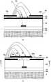
도 8(b)은, 도 6에 있어서의 절단선 D-D'에 따른 소자 기판(93)의 부분 단면도이며, 특히 하나의 소스선(32)과 그 소스선(32)의 양측에 마련된 2개의 서브 화소의 부분에 대응하는 단면도를 나타내고 있다. 한편, 도 8(a)은, 도 8(b)에 대응하는 비교예에 따른 소자 기판(95)의 부분 단면도이다.FIG. 8B is a partial cross-sectional view of the
우선, 비교예에 따른 소자 기판(95)의 구성에 대하여 간단히 설명한다.First, the configuration of the
하측 기판(1)상에는 게이트 절연막(50)이 설치되고, 또한, 게이트 절연막(50)상에는 제 1 절연막(51)이 설치된다. 제 1 절연막(51)상에는 소스선(32)이 지면 전방으로부터 지면 깊이측으로 연재하도록 설치된다. 소스선(32) 및 제 1 절연막(51)상에는 평탄화막으로서의 제 2 절연막(52)이 설치된다. 제 2 절연막(52)상에는 공통 전극(20)이 설치되고, 또한, 공통 전극(20)상에는 유전막으로서의 제 3 절연막(53)이 설치된다. 제 3 절연막(53) 상에 있어서, 소스선(32)의 양측에 대응하는 위치에는, 각각 화소 전극(10)이 설치된다. 또, 이하에서는, 설명의 편의상, 지면 좌측에 위치하는 화소 전극(10)을 「화소 전극(10)」이라 하며, 또한, 지면 우측에 위치하는 화소 전극(10)을 「화소 전극(10R)」이라 각각 칭한다. 이렇게 해서, 비교예에 따른 소자 기판(95)이 형성되어 있다.The
이상의 구성을 갖는 비교예에서는, 그 구동시, 동 도면에 도시하는 바와 같이 화소 전극(10)과 공통 전극(20)사이에서, 소자 기판(95)의 기판면에 대하여 대 략 평행한 방향 및 대략 수직인 방향(지면 상측 방향)으로 강한 전계 성분을 갖는 프린지 필드(전계 E)가 발생한다. 여기서, 예컨대, 화소 전극(10L)을 구동하는 전압이 높은 경우, 그것에 응해서 해당 화소 전극(10L)과 공통 전극(20) 사이에 발생하는 프린지 필드(전계 E)의 세기도 강하게 된다. 이것에 의해, 그 프린지 필드(전계 E)를 구성하는 일부의 전계 Ex가 인접하는 화소 전극(10R)으로까지 및 해당 화소 전극(10R)의 상측에 위치하는 액정 분자(4a)의 배향 상태에 악영향을 줄 가능성이 있다.In the comparative example having the above configuration, at the time of its driving, as shown in the figure, the direction and the direction substantially parallel to the substrate surface of the
이것에 대하여, 실시예 2에서는, 그와 같은 불량은 발생하지 않는다.On the other hand, in Example 2, such a defect does not arise.
즉, 실시예 2에서는, 그 구동시, 도 8(b)에 도시하는 바와 같이, 화소 전극(10)과, 소스선(32)의 상측에 마련되고 또한 평면적으로 겹치는 공통 전극(20)과의 사이에서 프린지 필드(전계 E)가 발생한다. 여기서, 실시예 2에 있어서, 예컨대, 화소 전극(10L)을 구동하는 전압이 높은 경우, 그것에 응해서 해당 화소 전극(10L)과 공통 전극(20) 사이에 발생하는 프린지 필드(전계 E)의 세기도 강하게 되지만, 그 프린지 필드(전계 E)는, 소스선(32)의 상측에 마련되고 또한 평면적으로 겹치는 공통 전극(20)의 존재에 의해서, 인접하는 화소 전극(10R)까지 미치지 않는다. 따라서, 상기한 비교예와 같은 문제점은 발생하지 않기 때문에, 인접하는 화소 전극(10R)의 상측에 위치하는 액정 분자(4a)의 배향 상태에 악영향을 주는 것을 방지할 수 있어, 양호한 표시 품질을 얻을 수 있고, 또한, 보다 고선명화를 실현할 수 있다. 또, 그 밖의 실시예 2의 작용 효과는 실시예 1과 마찬가지다.That is, in the second embodiment, at the time of driving, as shown in FIG. 8B, the
(변형예)(Variation)
상기의 실시예 1 및 실시예 2에서는, 본 발명을 투과형의 액정 장치에 적용하는 것으로 했지만, 이것에 한하지 않고, 본 발명을 반사형 또는 반투과 반사형의 액정 장치에 적용하는 것으로서도 상관없다.In Example 1 and Example 2 mentioned above, although this invention was applied to a transmissive liquid crystal device, it is not limited to this, It does not matter even if it applies to this reflective or semi-transmissive reflective liquid crystal device. .
또한, 상기의 실시예 1 및 실시예 2에서는, 본 발명을, LTPS형 TFT 소자(21)를 갖는 액정 장치에 적용했다. 이것에 한정되지 않고, 본 발명에서는, 그 취지를 일탈하지 않는 범위에 있어서, P-Si 형의 TFT 소자 또는 α-Si 형의 TFT 소자 등으로 대표되는 3단자형 소자, 혹은 TFD 소자에 대표되는 2단자형 비선형 소자에 본 발명을 적용하더라도 상관없다.In addition, in Example 1 and Example 2 mentioned above, this invention was applied to the liquid crystal device which has the LTPS type |
또한, 상기의 실시예 1에서는, 화소 전극(10)에 마련되는 각 슬릿(1Oa)은, 게이트선(33)의 제 2 배선(33b)의 연재 방향에 대하여 반시계 회전 방향으로 소정 각도만큼 회전시킨 방향으로 연재하도록 설치되었다. 이것에 한정되지 않고, 본 발명에서는, 화소 전극(10)에 마련되는 각 슬릿(10a)을, 게이트선(33)의 제 2 배선(33b)의 연재 방향으로 일정한 간격을 두고, 또한 소스선(32)의 연재 방향으로 연재하도록 마련하더라도 상관없다. 또한, 본 발명에서는, 실시예 2에 있어서, 공통 전극(20)에 마련되는 각 슬릿(20a)을, 게이트선(33)의 제 2 배선(33b)의 연재 방향으로 일정한 간격을 두고, 또한 소스선(32)의 연재 방향으로 연재하도록 마련하더라도 상관없다. 이들의 경우, 러빙 방향 R는, 소스선(32)의 연재 방향에 대하여 시계 회전 방향으로 소정 각도 θ, 바람직하게는 약 5°로 설정되어 있는 것이 좋다. 이것에 의해, 액정 분자(4a)를 프린지 필드(전계 E)에 의해서 각 슬릿(1Oa 또는 20a)과 대략 직교하는 방향으로 쉽게 재배향할 수 있다.In addition, in Example 1 mentioned above, each
또한, 실시예 2에서는, 착색층(6R 및 6B)의 각각에 대응하는 각 서브 화소에 대응하는 각 공통 전극(20)이, 소스선(32)과 평면적으로 겹치도록 형성하고, 또한, 착색층(6G)에 대응하는 서브 화소에 대응하는 공통 전극(20)이, 해당 서브 화소의 양측에 마련된 소스선(32)과는 평면적으로 겹치지 않도록 형성되었다. 이것에 한정되지 않고, 본 발명에서는, 공통 전극(20)은, 도 1에 있어서 각 횡방향(X 방향)으로 열을 이루는 서브 화소군과 대향하도록 스트라이프 형상으로 형성하더라도 상관없다. 이것에 의해, 도 1의 횡방향으로 서로 인접하는 화소 전극(10)의 사이에 위치하는 소스선(32)의 부분은 공통 전극(20)과 평면적으로 겹치는 것으로 되기 때문에, 임의의 서브 화소에 발생하는 프린지 필드(전계 E)가, 해당 서브 화소에 인접하는 다른 서브 화소에 주는 영향을 적게 할 수 있다.In addition, in Example 2, each
또한, 본 발명에서는, 실시예 2에 마련한 공통 전극선(20x)을, 수단에 따라 실시예 1에 마련하도록 하더라도 상관없다.In addition, in this invention, you may provide the
기타, 본 발명에서는, 그 취지를 일탈하지 않는 범위에 있어서 여러가지의 변형을 할 수 있다.In addition, in the present invention, various modifications can be made without departing from the spirit thereof.
(전자기기)(Electronics)
다음에, 본 발명의 실시예 1 또는 실시예 2에 따른 액정 장치(100, 200)를 적용가능한 전자기기의 구체예에 대하여 도 9를 참조하여 설명한다.Next, a specific example of the electronic device to which the
우선, 본 발명의 실시예 1 또는 실시예 2에 따른 액정 장치(100, 200)를, 가 반형의 퍼스널 컴퓨터(이른바 노트북 컴퓨터)의 표시부에 적용한 예에 대하여 설명한다. 도 9(a)는, 이 퍼스널 컴퓨터의 구성을 나타내는 사시도이다. 동 도면에 도시하는 바와 같이, 퍼스널 컴퓨터(710)는, 키보드(711)를 구비한 본체부(712)와, 본 발명에 따른 액정 표시 장치를 패널로서 적용한 표시부(713)를 구비하고 있다.First, an example in which the
계속해서, 본 발명의 실시예 1 또는 실시예 2에 따른 액정 장치(100, 200)를, 휴대 전화기의 표시부에 적용한 예에 대하여 설명한다. 도 9(b)는, 이 휴대 전화기의 구성을 나타내는 사시도이다. 동 도면에 도시하는 바와 같이, 휴대 전화기(720)는, 복수의 조작 버튼(721) 외에, 수화구(722), 송화구(723)와 함께, 본 발명의 실시예 1 또는 실시예 2에 따른 액정 장치(100, 200)를 적용한 표시부(724)를 구비한다.Subsequently, an example in which the
또, 본 발명의 실시예 1 또는 실시예 2에 따른 액정 장치(100, 200)를 적용가능한 전자기기로서는, 도 9(a)에 나타낸 퍼스널 컴퓨터나 도 9(b)에 나타낸 휴대 전화기 이외에도, 액정 텔레비젼, 뷰 파인더형·모니터 직시형의 비디오 테이프 레코더, 카네비게이션 장치, 페이저, 전자 수첩, 전자 계산기, 워드 프로세서, 워크 스테이션, 화상 전화, POS 단말, 디지털 스틸 카메라 등을 들 수 있다.In addition, as an electronic device to which the
본 발명에 따르면, 고개구율을 실현하는 것이 가능한 FFS 방식의 액정 장치 등을 제공할 수 있다.According to the present invention, it is possible to provide a FFS type liquid crystal device or the like which can realize a high opening ratio.
Claims (22)
Translated fromKoreanApplications Claiming Priority (4)
| Application Number | Priority Date | Filing Date | Title |
|---|---|---|---|
| JP2006017321 | 2006-01-26 | ||
| JPJP-P-2006-00017321 | 2006-01-26 | ||
| JP2006177829AJP2007226175A (en) | 2006-01-26 | 2006-06-28 | Liquid crystal device and electronic equipment |
| JPJP-P-2006-00177829 | 2006-06-28 |
Related Child Applications (2)
| Application Number | Title | Priority Date | Filing Date |
|---|---|---|---|
| KR1020080023389ADivisionKR20080031241A (en) | 2006-01-26 | 2008-03-13 | Liquid Crystal Devices and Electronics |
| KR1020080023383ADivisionKR20080031240A (en) | 2006-01-26 | 2008-03-13 | Liquid Crystal Devices and Electronics |
Publications (2)
| Publication Number | Publication Date |
|---|---|
| KR20070078389A KR20070078389A (en) | 2007-07-31 |
| KR100841153B1true KR100841153B1 (en) | 2008-06-24 |
Family
ID=37891753
Family Applications (3)
| Application Number | Title | Priority Date | Filing Date |
|---|---|---|---|
| KR1020070007969AActiveKR100841153B1 (en) | 2006-01-26 | 2007-01-25 | Liquid Crystal Devices and Electronics |
| KR1020080023383ACeasedKR20080031240A (en) | 2006-01-26 | 2008-03-13 | Liquid Crystal Devices and Electronics |
| KR1020080023389ACeasedKR20080031241A (en) | 2006-01-26 | 2008-03-13 | Liquid Crystal Devices and Electronics |
Family Applications After (2)
| Application Number | Title | Priority Date | Filing Date |
|---|---|---|---|
| KR1020080023383ACeasedKR20080031240A (en) | 2006-01-26 | 2008-03-13 | Liquid Crystal Devices and Electronics |
| KR1020080023389ACeasedKR20080031241A (en) | 2006-01-26 | 2008-03-13 | Liquid Crystal Devices and Electronics |
Country Status (5)
| Country | Link |
|---|---|
| US (1) | US20070171319A1 (en) |
| EP (2) | EP1983368A1 (en) |
| JP (1) | JP2007226175A (en) |
| KR (3) | KR100841153B1 (en) |
| TW (1) | TW200734735A (en) |
Families Citing this family (86)
| Publication number | Priority date | Publication date | Assignee | Title |
|---|---|---|---|---|
| JP4645488B2 (en)* | 2006-03-15 | 2011-03-09 | ソニー株式会社 | Liquid crystal device and electronic device |
| TWI545380B (en) | 2006-05-16 | 2016-08-11 | 半導體能源研究所股份有限公司 | Liquid crystal display device and semiconductor device |
| JP4932415B2 (en) | 2006-09-29 | 2012-05-16 | 株式会社半導体エネルギー研究所 | Semiconductor device |
| JP2008164787A (en) | 2006-12-27 | 2008-07-17 | Epson Imaging Devices Corp | Liquid crystal display device |
| JP5167780B2 (en)* | 2007-03-13 | 2013-03-21 | セイコーエプソン株式会社 | Electric field driving apparatus and electronic apparatus |
| US8018554B2 (en)* | 2007-03-28 | 2011-09-13 | Sony Corporation | Liquid crystal display device with internal retardation layer at reflection region and electronic apparatus |
| US8619225B2 (en)* | 2007-03-28 | 2013-12-31 | Japan Display West Inc. | Liquid crystal device with pixel electrode under the common electrode and thinner than drain electrode, method of manufacturing liquid crystal device, and electronic apparatus |
| JP4487318B2 (en)* | 2007-07-26 | 2010-06-23 | エプソンイメージングデバイス株式会社 | Liquid crystal display device and manufacturing method thereof |
| US8218116B2 (en)* | 2007-08-01 | 2012-07-10 | Sony Corporation | Liquid crystal display panel and manufacturing method thereof |
| US7903219B2 (en)* | 2007-08-16 | 2011-03-08 | Sony Corporation | Liquid crystal display device |
| JP5235363B2 (en) | 2007-09-04 | 2013-07-10 | 株式会社ジャパンディスプレイイースト | Liquid crystal display |
| JP5519101B2 (en)* | 2007-09-28 | 2014-06-11 | 株式会社ジャパンディスプレイ | Electronics |
| JP5072530B2 (en)* | 2007-10-23 | 2012-11-14 | 株式会社ジャパンディスプレイウェスト | Liquid crystal device and electronic device including the same |
| US8212954B2 (en)* | 2007-11-21 | 2012-07-03 | Sony Corporation | Liquid crystal display device |
| JP4600463B2 (en)* | 2007-11-21 | 2010-12-15 | ソニー株式会社 | Liquid crystal display |
| JP4442684B2 (en) | 2007-11-29 | 2010-03-31 | エプソンイメージングデバイス株式会社 | Liquid crystal display device and manufacturing method thereof |
| JP2009151285A (en)* | 2007-11-30 | 2009-07-09 | Epson Imaging Devices Corp | Liquid crystal display device and method for manufacturing the same |
| JP5285280B2 (en) | 2008-01-07 | 2013-09-11 | 株式会社ジャパンディスプレイウェスト | Liquid crystal display device and method of manufacturing liquid crystal display device |
| JP4678031B2 (en)* | 2008-01-11 | 2011-04-27 | ソニー株式会社 | Liquid crystal device and electronic device |
| JP5255853B2 (en)* | 2008-01-24 | 2013-08-07 | 株式会社ジャパンディスプレイウェスト | Liquid crystal display device and manufacturing method thereof |
| JP5100418B2 (en)* | 2008-01-28 | 2012-12-19 | 株式会社ジャパンディスプレイウェスト | Liquid crystal display |
| JP2009198703A (en)* | 2008-02-20 | 2009-09-03 | Sony Corp | Liquid crystal display device and method of manufacturing the same |
| JP5246782B2 (en) | 2008-03-06 | 2013-07-24 | 株式会社ジャパンディスプレイウェスト | Liquid crystal device and electronic device |
| JP5175127B2 (en)* | 2008-03-28 | 2013-04-03 | 株式会社ジャパンディスプレイウェスト | Liquid crystal display |
| KR100975470B1 (en)* | 2008-04-14 | 2010-08-11 | 하이디스 테크놀로지 주식회사 | FS mode LCD |
| JP2009265512A (en)* | 2008-04-28 | 2009-11-12 | Sony Corp | Liquid crystal display apparatus |
| KR20100005883A (en)* | 2008-07-08 | 2010-01-18 | 삼성전자주식회사 | Array substrate and liquid crystal display apparatus having the same |
| JP2010060967A (en)* | 2008-09-05 | 2010-03-18 | Epson Imaging Devices Corp | Liquid crystal display device and electronic apparatus |
| KR101582947B1 (en)* | 2008-09-17 | 2016-01-08 | 삼성디스플레이 주식회사 | Liquid crystal display |
| JP5392670B2 (en) | 2008-12-01 | 2014-01-22 | 株式会社ジャパンディスプレイ | Liquid crystal display device and manufacturing method thereof |
| JP5389529B2 (en)* | 2009-05-20 | 2014-01-15 | 株式会社ジャパンディスプレイ | Liquid crystal display device and manufacturing method thereof |
| KR101654763B1 (en)* | 2009-06-08 | 2016-09-07 | 엘지디스플레이 주식회사 | Liquid crystal display panel and liquid crystal display device having the same |
| KR101219821B1 (en)* | 2009-08-17 | 2013-01-08 | 하이디스 테크놀로지 주식회사 | Fringe field switching mode liquid crystal display and manufacturing method thereof |
| KR101631620B1 (en)* | 2009-10-13 | 2016-06-17 | 엘지디스플레이 주식회사 | Fringe field switching liquid crystal display device and method of fabricating the same |
| US8804081B2 (en)* | 2009-12-18 | 2014-08-12 | Samsung Display Co., Ltd. | Liquid crystal display device with electrode having opening over thin film transistor |
| KR101695285B1 (en)* | 2009-12-22 | 2017-01-24 | 엘지디스플레이 주식회사 | Liquid Crystal Display Device and Method for Manufacturing the Same |
| WO2011155469A1 (en)* | 2010-06-07 | 2011-12-15 | 株式会社アルバック | Liquid crystal display device and method of manufacturing liquid display device, and electrode substrate for liquid crystal display device |
| WO2011155470A1 (en)* | 2010-06-07 | 2011-12-15 | 株式会社アルバック | Liquid crystal display device and method of manufacturing liquid crystal display device, and electrode substrate for liquid crystal display device |
| WO2012046632A1 (en)* | 2010-10-06 | 2012-04-12 | シャープ株式会社 | Array substrate and display device using said array substrate |
| CN202033562U (en)* | 2011-04-29 | 2011-11-09 | 京东方科技集团股份有限公司 | Liquid crystal display array base plate |
| KR101881277B1 (en)* | 2011-05-18 | 2018-07-24 | 엘지디스플레이 주식회사 | Liquid Crystal Display Device And Method Of Manufacturing The Same |
| CN102262326B (en)* | 2011-08-02 | 2014-08-13 | 深超光电(深圳)有限公司 | In-plane switching LCD panel |
| JP5961876B2 (en)* | 2011-08-04 | 2016-08-02 | 株式会社ジャパンディスプレイ | Liquid crystal display |
| KR101870986B1 (en)* | 2011-09-19 | 2018-06-26 | 엘지디스플레이 주식회사 | Method for fabricating thin film transistor array substrate |
| US8189158B1 (en) | 2011-09-29 | 2012-05-29 | Hannstar Display Corp. | Fringe field switching liquid crystal display apparatus |
| KR101941439B1 (en)* | 2011-10-04 | 2019-01-24 | 엘지디스플레이 주식회사 | Oxide Thin Film Transistor Array Substrate and the method of manufacturing the same |
| US9323112B2 (en) | 2011-10-12 | 2016-04-26 | Japan Display Inc. | Liquid crystal display and electronic apparatus having electrodes with openings therein |
| CN102629055B (en) | 2011-10-24 | 2015-06-03 | 北京京东方光电科技有限公司 | Array substrate and color film substrate of display device and manufacture method thereof |
| KR101900814B1 (en)* | 2011-11-30 | 2018-09-20 | 엘지디스플레이 주식회사 | Array substrate for fringe field switching mode liquid crystal display device |
| KR101953141B1 (en)* | 2011-12-14 | 2019-03-04 | 엘지디스플레이 주식회사 | Array substrate for fringe field switching mode liquid crystal display device and method for fabricating the same |
| KR101524449B1 (en) | 2011-12-22 | 2015-06-02 | 엘지디스플레이 주식회사 | Liquid crystal display device and Method for manufacturing the same |
| KR101279297B1 (en)* | 2011-12-26 | 2013-06-26 | 하이디스 테크놀로지 주식회사 | Ffs mode liquid crystal display and method for manufacturing thereof |
| KR101611923B1 (en) | 2012-02-27 | 2016-04-14 | 엘지디스플레이 주식회사 | Liquid crystal display device and method of fabricating the same |
| KR101622655B1 (en) | 2012-03-14 | 2016-05-19 | 엘지디스플레이 주식회사 | Liquid crystal display device and method of fabricating the same |
| TW201341916A (en) | 2012-04-12 | 2013-10-16 | Innocom Tech Shenzhen Co Ltd | Pixel structure and liquid crystal display structure using same |
| KR101936773B1 (en)* | 2012-07-03 | 2019-01-09 | 엘지디스플레이 주식회사 | Method for manufacturing liquid crystal display device |
| KR102099262B1 (en) | 2012-07-11 | 2020-04-09 | 가부시키가이샤 한도오따이 에네루기 켄큐쇼 | Liquid crystal display device and method for driving the same |
| US9239501B2 (en) | 2012-07-26 | 2016-01-19 | Innocom Technology(Shenzhen) Co., Ltd. | Liquid crystal display device |
| JP2014174402A (en)* | 2013-03-11 | 2014-09-22 | Japan Display Inc | Liquid crystal display device |
| JP6230253B2 (en) | 2013-04-03 | 2017-11-15 | 三菱電機株式会社 | TFT array substrate and manufacturing method thereof |
| JP6173049B2 (en) | 2013-06-04 | 2017-08-02 | 三菱電機株式会社 | Display panel, manufacturing method thereof, and liquid crystal display panel |
| TWI636309B (en)* | 2013-07-25 | 2018-09-21 | 日商半導體能源研究所股份有限公司 | Liquid crystal display device and electronic device |
| TWI511303B (en)* | 2013-08-30 | 2015-12-01 | Ye Xin Technology Consulting Co Ltd | Array substrate of liquid crystal display |
| KR101668381B1 (en) | 2013-09-30 | 2016-10-31 | 삼성디스플레이 주식회사 | Liquid crystal display and method of manufacturing the same |
| KR102198111B1 (en) | 2013-11-04 | 2021-01-05 | 삼성디스플레이 주식회사 | Thin film transistor array panel and manufacturing method thereof |
| JP6308757B2 (en) | 2013-11-20 | 2018-04-11 | 三菱電機株式会社 | Liquid crystal display panel and method for manufacturing liquid crystal display panel |
| KR102051113B1 (en)* | 2013-12-18 | 2019-12-03 | 삼성디스플레이 주식회사 | Liquid crystal display and method of manufacturing the same |
| JP6336762B2 (en) | 2014-01-24 | 2018-06-06 | 株式会社ジャパンディスプレイ | Liquid crystal display |
| JP5809722B2 (en)* | 2014-03-03 | 2015-11-11 | 株式会社半導体エネルギー研究所 | Liquid crystal display |
| KR102174220B1 (en) | 2014-05-02 | 2020-11-05 | 삼성디스플레이 주식회사 | Liquid crystal display |
| KR102261760B1 (en) | 2014-07-29 | 2021-06-07 | 삼성디스플레이 주식회사 | Thin film transistor array panel and manufacturing method thereof |
| CN110262149B (en)* | 2015-02-12 | 2022-06-21 | 群创光电股份有限公司 | display panel |
| TWI548921B (en) | 2015-02-12 | 2016-09-11 | 群創光電股份有限公司 | Display panel |
| JP2016148807A (en)* | 2015-02-13 | 2016-08-18 | 株式会社ジャパンディスプレイ | Liquid crystal display device |
| KR20160114510A (en)* | 2015-03-24 | 2016-10-05 | 가부시키가이샤 한도오따이 에네루기 켄큐쇼 | Touch panel |
| KR102328918B1 (en)* | 2015-05-21 | 2021-11-19 | 엘지디스플레이 주식회사 | Array substrate and liquid cristal display device including thereof |
| KR102563157B1 (en)* | 2015-08-26 | 2023-08-04 | 엘지디스플레이 주식회사 | Thin film transistor and display device |
| KR102346086B1 (en)* | 2015-09-17 | 2022-01-03 | 엘지디스플레이 주식회사 | Liquid crystal display device having a compensting thin film transistor |
| TWI595298B (en)* | 2015-12-14 | 2017-08-11 | 群創光電股份有限公司 | Display panel |
| JP2017215511A (en)* | 2016-06-01 | 2017-12-07 | 株式会社ジャパンディスプレイ | Display device |
| US10777587B2 (en)* | 2016-09-02 | 2020-09-15 | Sharp Kabushiki Kaisha | Active matrix substrate and display device provided with active matrix substrate |
| KR101948717B1 (en)* | 2017-10-23 | 2019-02-18 | 삼성디스플레이 주식회사 | Display substrate, method for manufacturing the same, and display apparatus having the same |
| JP7043297B2 (en)* | 2018-03-09 | 2022-03-29 | 株式会社ジャパンディスプレイ | Display device |
| CN114267776A (en)* | 2021-12-16 | 2022-04-01 | 惠州华星光电显示有限公司 | Display panel, manufacturing method and mobile terminal |
| CN117957489A (en)* | 2022-08-31 | 2024-04-30 | 京东方科技集团股份有限公司 | Array substrate and manufacturing method thereof, liquid crystal panel |
| WO2025065188A1 (en)* | 2023-09-25 | 2025-04-03 | 京东方科技集团股份有限公司 | Array substrate, manufacturing method therefor, and display apparatus |
Citations (7)
| Publication number | Priority date | Publication date | Assignee | Title |
|---|---|---|---|---|
| JP2000111957A (en) | 1998-08-03 | 2000-04-21 | Nec Corp | Liquid crystal display device and its manufacture |
| US20010046027A1 (en)* | 1999-09-03 | 2001-11-29 | Ya-Hsiang Tai | Liquid crystal display having stripe-shaped common electrodes formed above plate-shaped pixel electrodes |
| KR20020070756A (en)* | 2001-02-28 | 2002-09-11 | 가부시키가이샤 히타치세이사쿠쇼 | Liquid crystal display |
| KR20030049986A (en)* | 2001-12-18 | 2003-06-25 | 엘지.필립스 엘시디 주식회사 | transflective liquid crystal display and manufacturing method thereof |
| KR20030079809A (en)* | 2002-04-04 | 2003-10-10 | 엔이씨 엘씨디 테크놀로지스, 엘티디. | In-plane switching mode active matrix type liquid crystal display device and method of fabricating the same |
| KR20040062015A (en)* | 2002-12-31 | 2004-07-07 | 엘지.필립스 엘시디 주식회사 | array substrate for liquid crystal display and fabricating method of the same |
| KR20060117465A (en)* | 2005-05-11 | 2006-11-17 | 비오이 하이디스 테크놀로지 주식회사 | Transflective fringe field switching mode liquid crystal display |
Family Cites Families (98)
| Publication number | Priority date | Publication date | Assignee | Title |
|---|---|---|---|---|
| US3841348A (en)* | 1969-06-12 | 1974-10-15 | Westinghouse Electric Corp | Fluid pressure control apparatus |
| US3734133A (en)* | 1970-12-02 | 1973-05-22 | Rkl Controls | Diverter pinch valve |
| US3698681A (en)* | 1970-12-15 | 1972-10-17 | Illinois Tool Works | On-off clamp for i. v. systems |
| US3938543A (en)* | 1973-05-21 | 1976-02-17 | Sorenson Gerald T | Fluid control system |
| US3823724A (en)* | 1973-05-25 | 1974-07-16 | Med Lab Computer Services Inc | Controlling flow of medical fluids |
| SE383402B (en)* | 1973-10-15 | 1976-03-08 | Saab Scania Ab | SPRINKLE VALVE |
| US3942228A (en)* | 1974-07-19 | 1976-03-09 | Buckman Thomas P | Tubing clamp |
| US4044996A (en)* | 1974-10-16 | 1977-08-30 | Heiichi Kodaira | Valve means |
| US3988001A (en)* | 1975-07-21 | 1976-10-26 | Sybron Corporation | Variable flow control valve for use with dental syringes and the like |
| US4000662A (en)* | 1975-09-05 | 1977-01-04 | Clark Equipment Company | Multiple input transmission |
| DE2558058C3 (en)* | 1975-12-22 | 1979-08-30 | Blasius 7455 Jungingen Speidel | Drain valve for blood pressure meters and the like |
| US4091815A (en)* | 1976-07-06 | 1978-05-30 | Larsen Otis M | Flexible tube clamp |
| US4323173A (en)* | 1976-11-17 | 1982-04-06 | American Beverage Control | Beverage dispenser pumping system to maintain live pressure after shut off |
| US4084786A (en)* | 1977-01-28 | 1978-04-18 | Tom Walters | Valves |
| US4184815A (en)* | 1977-03-14 | 1980-01-22 | Extracorporeal Medical Specialties, Inc. | Roller pump rotor with integral spring arms |
| DE2725575A1 (en)* | 1977-06-07 | 1978-12-21 | Karl Hehl | DEVICE FOR THE ALTERNATE CONNECTION OF A MANOMETER TO DIFFERENT PRESSURE MEASURING POINTS |
| US4186618A (en)* | 1977-08-05 | 1980-02-05 | Eaton Corporation | Transmission input decelerating and reversing mechanism |
| US4340202A (en)* | 1977-10-07 | 1982-07-20 | Emerson Electric Co. | Four way valve |
| US4144774A (en)* | 1977-11-21 | 1979-03-20 | Westran Corporation | Actuator device |
| US4224958A (en)* | 1977-12-19 | 1980-09-30 | Kaplan Stephen J | Valve device for diverting and combining fluid flows |
| US4193174A (en)* | 1978-04-11 | 1980-03-18 | Portex, Inc. | Lever and fulcrum clamping assembly |
| US4230149A (en)* | 1978-05-22 | 1980-10-28 | Eaton Corporation | Fluid flow regulating valve and system |
| GB1605067A (en)* | 1978-05-30 | 1981-12-16 | Massey Ferguson Services Nv | Transmission having a twospeed planetary gear set |
| US4191214A (en)* | 1978-07-07 | 1980-03-04 | Forney Engineering Company | Sequential operating mechanism for valves |
| US4227548A (en)* | 1979-02-27 | 1980-10-14 | Botnick Irlin H | Multiple control valve for mixing fluids |
| US4247076A (en)* | 1979-04-16 | 1981-01-27 | Abbott Laboratories | Toggle action tubing clamp |
| US4282902A (en)* | 1979-05-04 | 1981-08-11 | Becton Dickinson & Company | Valve apparatus for simultaneous control of a plurality of fluid paths |
| US4401626A (en)* | 1979-05-17 | 1983-08-30 | Phillips Petroleum Company | Spray device useful in carbon black reactor |
| US4243063A (en)* | 1979-09-14 | 1981-01-06 | American Standard Inc. | Mixing valve |
| US4253491A (en)* | 1980-02-25 | 1981-03-03 | Eaton Corporation | Fluid flow regulating valve and system |
| EP0052100B1 (en)* | 1980-05-19 | 1984-09-05 | Ipanema Company | Power drive line having a wide range of speed ratios |
| US4474309A (en)* | 1981-10-22 | 1984-10-02 | Oximetrix, Inc. | Stepping motor control procedure for achieving variable rate, quasi-continuous fluid infusion |
| US4445826A (en)* | 1982-01-22 | 1984-05-01 | Polaroid Corporation | Peristaltic pump apparatus |
| US5190071A (en)* | 1982-03-02 | 1993-03-02 | Akos Sule | Pinch valve assembly |
| US4590998A (en)* | 1983-09-27 | 1986-05-27 | Hopper Bobby E | Tubing valve |
| US4563175A (en)* | 1983-12-19 | 1986-01-07 | Lafond Margaret | Multiple syringe pump |
| US4533113A (en)* | 1984-04-24 | 1985-08-06 | Francart Jr Armand | Compact high torque rotary valve operator for simultaneous actuation of multiple rotary valves |
| DE3429660A1 (en)* | 1984-08-11 | 1986-02-13 | Adam Opel AG, 6090 Rüsselsheim | ARRANGEMENT FOR OPERATING A VALVE |
| US4596374A (en)* | 1984-11-29 | 1986-06-24 | Baxter Travenol Laboratories, Inc. | Clamp valve |
| GB8526055D0 (en)* | 1985-10-22 | 1985-11-27 | Ici Plc | Electricity production |
| US4697785A (en)* | 1986-04-14 | 1987-10-06 | Tuseth Robert D | Clamp for regulating flow of parenteral solutions |
| US4946434A (en)* | 1986-07-22 | 1990-08-07 | Haemonetics Corporation | Disposable manifold and valve |
| US5087018A (en)* | 1987-03-20 | 1992-02-11 | Bissell Inc. | Fluid flow control valve |
| US4757598A (en)* | 1987-11-23 | 1988-07-19 | Emerson Electric Co. | Two speed transmission for power driven threading machine |
| US5074756A (en)* | 1988-05-17 | 1991-12-24 | Patient Solutions, Inc. | Infusion device with disposable elements |
| US4903944A (en)* | 1989-01-31 | 1990-02-27 | Snap-On Tools Corporation | Valve assembly and method |
| US4944485A (en)* | 1989-08-28 | 1990-07-31 | Ivac Corporation | Clamp for flexible tubing |
| US4989641A (en)* | 1989-10-11 | 1991-02-05 | Santa Fe Energy Co. | Rotary selector valve |
| SE464747B (en)* | 1990-02-23 | 1991-06-10 | Atlas Copco Tools Ab | TWO SPEED POWER TRANSMISSION FOR A MOTOR POWER TOOL |
| DE4014602A1 (en)* | 1990-05-07 | 1991-11-14 | Max Planck Gesellschaft | DOSING DEVICE WITH RADIAL ARRANGEMENT OF VALVES |
| JPH0810019B2 (en)* | 1990-12-26 | 1996-01-31 | 日本電池株式会社 | Planetary gear shifting mechanism incorporating a one-way clutch |
| US5083741A (en)* | 1991-05-10 | 1992-01-28 | Block Medical, Inc. | IV tube clamp with extended clamping surface |
| US5152497A (en)* | 1991-05-13 | 1992-10-06 | Timberline Northwest, Inc. | Squeeze-off clamp |
| US5300034A (en)* | 1992-07-29 | 1994-04-05 | Minnesota Mining And Manufacturing Company | Iv injection site for the reception of a blunt cannula |
| US5330000A (en)* | 1992-09-22 | 1994-07-19 | Halliburton Company | Squeeze packer latch |
| US5402823A (en)* | 1992-12-07 | 1995-04-04 | George S. Cole & Associates, Incorporated | Pinch valve |
| US5347992A (en)* | 1993-01-22 | 1994-09-20 | Karl Storz Endoscopy America, Inc. | Single axis three way selector valve for endoscopes |
| US5413566A (en)* | 1993-03-16 | 1995-05-09 | Micropump Corporation | Line clamp |
| CA2118979C (en)* | 1993-03-18 | 2003-02-25 | Spencer M. Nimberger | Sampling pump |
| US5419684A (en)* | 1993-06-14 | 1995-05-30 | Minnesota Mining And Manufacturing Company | Infusion pump with reversible motor and method of use |
| US5297773A (en)* | 1993-07-16 | 1994-03-29 | Fluoroware, Inc. | Plastic valve with flexible tube and tube squeezing apparatus |
| US5478290A (en)* | 1994-01-28 | 1995-12-26 | Fairfield Manufacturing Co., Inc. | Two speed high shift transmission |
| US5658133A (en)* | 1994-03-09 | 1997-08-19 | Baxter International Inc. | Pump chamber back pressure dissipation apparatus and method |
| US5630710A (en)* | 1994-03-09 | 1997-05-20 | Baxter International Inc. | Ambulatory infusion pump |
| DE4442352C1 (en)* | 1994-11-29 | 1995-12-21 | Braun Melsungen Ag | Valve arrangement provided in connector for use e.g. with cannula |
| US5620025A (en)* | 1994-12-01 | 1997-04-15 | Associated Universities, Inc. | Multi-port valve |
| JPH09112567A (en)* | 1995-10-23 | 1997-05-02 | Minolta Co Ltd | Sliding joint using coil spring |
| US5723918A (en)* | 1996-03-08 | 1998-03-03 | Honeywell Inc. | Bi-directional actuator using a random direction AC motor |
| US5746251A (en)* | 1996-05-23 | 1998-05-05 | Bullard; Horace | Multi-port fluid valve |
| JP3763166B2 (en)* | 1996-07-10 | 2006-04-05 | 株式会社デンソー | Reduction gear |
| US5865915A (en)* | 1996-08-07 | 1999-02-02 | Spartech Industries, Inc. | Bi-directional anti-slip drive wheel assembly |
| US5735175A (en)* | 1996-10-18 | 1998-04-07 | New Venture Gear, Inc. | Multi-speed manual transaxle |
| US5712548A (en)* | 1997-01-16 | 1998-01-27 | Eti Systems, Inc. | Bi-directional motor actuator |
| US5937980A (en)* | 1997-02-24 | 1999-08-17 | Dana Corporation | Bi-directional one-way clutch |
| US5924324A (en)* | 1997-10-09 | 1999-07-20 | Ut Automotive Dearborn, Inc. | Movable gear drive windshield wiper |
| JP4044187B2 (en)* | 1997-10-20 | 2008-02-06 | 株式会社半導体エネルギー研究所 | Active matrix display device and manufacturing method thereof |
| JP3519310B2 (en)* | 1998-06-12 | 2004-04-12 | シャープ株式会社 | Liquid crystal display |
| KR100325079B1 (en) | 1999-12-22 | 2002-03-02 | 주식회사 현대 디스플레이 테크놀로지 | Method of manufacturing lcd having high aperture ratio and high transmittance |
| KR20020002052A (en)* | 2000-06-29 | 2002-01-09 | 주식회사 현대 디스플레이 테크놀로지 | Method for manufacturing fringe field switching mode lcd |
| KR100482468B1 (en) | 2000-10-10 | 2005-04-14 | 비오이 하이디스 테크놀로지 주식회사 | Fringe field switching mode lcd |
| TW575775B (en)* | 2001-01-29 | 2004-02-11 | Hitachi Ltd | Liquid crystal display device |
| US6784966B2 (en)* | 2001-03-06 | 2004-08-31 | Seiko Epson Corp. | Liquid crystal device, projection type display and electronic equipment |
| KR100471397B1 (en)* | 2001-05-31 | 2005-02-21 | 비오이 하이디스 테크놀로지 주식회사 | Apparatus for fringe field switching liquid crystal display and method for manufacturing the same |
| TWI298110B (en)* | 2001-07-31 | 2008-06-21 | Hitachi Ltd | Liquid crystal display device |
| TWI271573B (en)* | 2001-08-22 | 2007-01-21 | Advanced Display Kk | Liquid crystal display device and method of producing the same |
| KR100507280B1 (en)* | 2001-08-29 | 2005-08-09 | 비오이 하이디스 테크놀로지 주식회사 | Fringe field switching mode liquid crystal display |
| JP2003140188A (en)* | 2001-11-07 | 2003-05-14 | Hitachi Ltd | Liquid crystal display |
| JP4162890B2 (en)* | 2001-12-27 | 2008-10-08 | 株式会社日立製作所 | Liquid crystal display |
| JP4047586B2 (en)* | 2002-01-10 | 2008-02-13 | Nec液晶テクノロジー株式会社 | Horizontal electric field type active matrix liquid crystal display device |
| JP3881248B2 (en)* | 2002-01-17 | 2007-02-14 | 株式会社日立製作所 | Liquid crystal display device and image display device |
| JP2003295207A (en)* | 2002-03-29 | 2003-10-15 | Nec Lcd Technologies Ltd | In-plane switching type active matrix liquid crystal display |
| JP3971778B2 (en)* | 2003-07-14 | 2007-09-05 | 株式会社 日立ディスプレイズ | Display device |
| JP2005057242A (en)* | 2003-07-18 | 2005-03-03 | Seiko Epson Corp | Thin film transistor, active matrix substrate, display device, and electronic device |
| KR20050030788A (en)* | 2003-09-26 | 2005-03-31 | 비오이 하이디스 테크놀로지 주식회사 | Method for fabricating fringe field switching liquid crystal display |
| JP4381782B2 (en)* | 2003-11-18 | 2009-12-09 | 株式会社 日立ディスプレイズ | Liquid crystal display |
| JP4326307B2 (en)* | 2003-11-19 | 2009-09-02 | 株式会社 日立ディスプレイズ | Liquid crystal display |
| JP4572854B2 (en)* | 2006-03-29 | 2010-11-04 | ソニー株式会社 | Liquid crystal device and electronic device |
| JP4404084B2 (en)* | 2006-10-31 | 2010-01-27 | エプソンイメージングデバイス株式会社 | Active matrix liquid crystal display device |
- 2006
- 2006-06-28JPJP2006177829Apatent/JP2007226175A/enactivePending
- 2007
- 2007-01-12USUS11/652,623patent/US20070171319A1/ennot_activeAbandoned
- 2007-01-24EPEP08075565Apatent/EP1983368A1/ennot_activeWithdrawn
- 2007-01-24EPEP07250291Apatent/EP1813979A3/ennot_activeCeased
- 2007-01-25KRKR1020070007969Apatent/KR100841153B1/enactiveActive
- 2007-01-25TWTW096102880Apatent/TW200734735A/enunknown
- 2008
- 2008-03-13KRKR1020080023383Apatent/KR20080031240A/ennot_activeCeased
- 2008-03-13KRKR1020080023389Apatent/KR20080031241A/ennot_activeCeased
Patent Citations (7)
| Publication number | Priority date | Publication date | Assignee | Title |
|---|---|---|---|---|
| JP2000111957A (en) | 1998-08-03 | 2000-04-21 | Nec Corp | Liquid crystal display device and its manufacture |
| US20010046027A1 (en)* | 1999-09-03 | 2001-11-29 | Ya-Hsiang Tai | Liquid crystal display having stripe-shaped common electrodes formed above plate-shaped pixel electrodes |
| KR20020070756A (en)* | 2001-02-28 | 2002-09-11 | 가부시키가이샤 히타치세이사쿠쇼 | Liquid crystal display |
| KR20030049986A (en)* | 2001-12-18 | 2003-06-25 | 엘지.필립스 엘시디 주식회사 | transflective liquid crystal display and manufacturing method thereof |
| KR20030079809A (en)* | 2002-04-04 | 2003-10-10 | 엔이씨 엘씨디 테크놀로지스, 엘티디. | In-plane switching mode active matrix type liquid crystal display device and method of fabricating the same |
| KR20040062015A (en)* | 2002-12-31 | 2004-07-07 | 엘지.필립스 엘시디 주식회사 | array substrate for liquid crystal display and fabricating method of the same |
| KR20060117465A (en)* | 2005-05-11 | 2006-11-17 | 비오이 하이디스 테크놀로지 주식회사 | Transflective fringe field switching mode liquid crystal display |
Also Published As
| Publication number | Publication date |
|---|---|
| TW200734735A (en) | 2007-09-16 |
| EP1813979A3 (en) | 2007-09-05 |
| KR20070078389A (en) | 2007-07-31 |
| KR20080031240A (en) | 2008-04-08 |
| US20070171319A1 (en) | 2007-07-26 |
| EP1983368A1 (en) | 2008-10-22 |
| EP1813979A2 (en) | 2007-08-01 |
| JP2007226175A (en) | 2007-09-06 |
| KR20080031241A (en) | 2008-04-08 |
Similar Documents
| Publication | Publication Date | Title |
|---|---|---|
| KR100841153B1 (en) | Liquid Crystal Devices and Electronics | |
| KR100940416B1 (en) | Liquid Crystal Devices and Electronics | |
| KR100892535B1 (en) | Liquid crystal device and electronic apparatus | |
| JP4717672B2 (en) | Liquid crystal device and electronic device | |
| US7688408B2 (en) | Liquid crystal device and electronic apparatus | |
| CN101008750A (en) | Liquid crystal devices and electronic equipment | |
| TWI381231B (en) | Liquid crystal display device | |
| JP4607158B2 (en) | Liquid crystal display device and electronic device | |
| JP3534097B2 (en) | Liquid crystal device and electronic equipment provided with the liquid crystal device | |
| JP2007226200A (en) | Liquid crystal device, and electronic device | |
| JP2007058007A (en) | Liquid crystal device and electronic apparatus | |
| JP2009075421A (en) | Liquid crystal device and electronic equipment | |
| JP2007094089A (en) | Electrooptical device and electronic equipment | |
| US20150131036A1 (en) | Liquid crystal display | |
| JP2007226199A (en) | Liquid crystal device, and electronic equipment | |
| JP2007094025A (en) | Electrooptic device and electronic equipment | |
| JP2007086506A (en) | Electrooptical device and electronic equipment | |
| JP2008225337A (en) | Liquid crystal device and electronic apparatus | |
| JP4552780B2 (en) | Electro-optical device and electronic apparatus | |
| JP2008233312A (en) | Liquid crystal device and electronic equipment | |
| JP2007094029A (en) | Electrooptical apparatus and electronic device | |
| JP2007286122A (en) | Color filter substrate, liquid crystal device, and electronic apparatus | |
| JP2007114337A (en) | Electrooptical apparatus and electronic apparatus | |
| JP2007279276A (en) | Liquid crystal device and electronic equipment | |
| JP2008203607A (en) | ELECTRO-OPTICAL DEVICE, ITS MANUFACTURING METHOD, AND ELECTRONIC DEVICE |
Legal Events
| Date | Code | Title | Description |
|---|---|---|---|
| A201 | Request for examination | ||
| PA0109 | Patent application | St.27 status event code:A-0-1-A10-A12-nap-PA0109 | |
| PA0201 | Request for examination | St.27 status event code:A-1-2-D10-D11-exm-PA0201 | |
| R18-X000 | Changes to party contact information recorded | St.27 status event code:A-3-3-R10-R18-oth-X000 | |
| PG1501 | Laying open of application | St.27 status event code:A-1-1-Q10-Q12-nap-PG1501 | |
| D13-X000 | Search requested | St.27 status event code:A-1-2-D10-D13-srh-X000 | |
| D14-X000 | Search report completed | St.27 status event code:A-1-2-D10-D14-srh-X000 | |
| E902 | Notification of reason for refusal | ||
| PE0902 | Notice of grounds for rejection | St.27 status event code:A-1-2-D10-D21-exm-PE0902 | |
| T11-X000 | Administrative time limit extension requested | St.27 status event code:U-3-3-T10-T11-oth-X000 | |
| A107 | Divisional application of patent | ||
| E13-X000 | Pre-grant limitation requested | St.27 status event code:A-2-3-E10-E13-lim-X000 | |
| P11-X000 | Amendment of application requested | St.27 status event code:A-2-2-P10-P11-nap-X000 | |
| P13-X000 | Application amended | St.27 status event code:A-2-2-P10-P13-nap-X000 | |
| PA0107 | Divisional application | St.27 status event code:A-0-1-A10-A18-div-PA0107 St.27 status event code:A-0-1-A10-A16-div-PA0107 | |
| E701 | Decision to grant or registration of patent right | ||
| PE0701 | Decision of registration | St.27 status event code:A-1-2-D10-D22-exm-PE0701 | |
| GRNT | Written decision to grant | ||
| PR0701 | Registration of establishment | St.27 status event code:A-2-4-F10-F11-exm-PR0701 | |
| PR1002 | Payment of registration fee | St.27 status event code:A-2-2-U10-U11-oth-PR1002 Fee payment year number:1 | |
| PG1601 | Publication of registration | St.27 status event code:A-4-4-Q10-Q13-nap-PG1601 | |
| PN2301 | Change of applicant | St.27 status event code:A-5-5-R10-R11-asn-PN2301 | |
| PN2301 | Change of applicant | St.27 status event code:A-5-5-R10-R14-asn-PN2301 | |
| PR1001 | Payment of annual fee | St.27 status event code:A-4-4-U10-U11-oth-PR1001 Fee payment year number:4 | |
| PR1001 | Payment of annual fee | St.27 status event code:A-4-4-U10-U11-oth-PR1001 Fee payment year number:5 | |
| PN2301 | Change of applicant | St.27 status event code:A-5-5-R10-R11-asn-PN2301 | |
| PN2301 | Change of applicant | St.27 status event code:A-5-5-R10-R14-asn-PN2301 | |
| FPAY | Annual fee payment | Payment date:20130607 Year of fee payment:6 | |
| PR1001 | Payment of annual fee | St.27 status event code:A-4-4-U10-U11-oth-PR1001 Fee payment year number:6 | |
| FPAY | Annual fee payment | Payment date:20140610 Year of fee payment:7 | |
| PR1001 | Payment of annual fee | St.27 status event code:A-4-4-U10-U11-oth-PR1001 Fee payment year number:7 | |
| FPAY | Annual fee payment | Payment date:20150605 Year of fee payment:8 | |
| PR1001 | Payment of annual fee | St.27 status event code:A-4-4-U10-U11-oth-PR1001 Fee payment year number:8 | |
| FPAY | Annual fee payment | Payment date:20160613 Year of fee payment:9 | |
| PR1001 | Payment of annual fee | St.27 status event code:A-4-4-U10-U11-oth-PR1001 Fee payment year number:9 | |
| FPAY | Annual fee payment | Payment date:20170609 Year of fee payment:10 | |
| PR1001 | Payment of annual fee | St.27 status event code:A-4-4-U10-U11-oth-PR1001 Fee payment year number:10 | |
| PR1001 | Payment of annual fee | St.27 status event code:A-4-4-U10-U11-oth-PR1001 Fee payment year number:11 | |
| PR1001 | Payment of annual fee | St.27 status event code:A-4-4-U10-U11-oth-PR1001 Fee payment year number:12 | |
| PR1001 | Payment of annual fee | St.27 status event code:A-4-4-U10-U11-oth-PR1001 Fee payment year number:13 | |
| PR1001 | Payment of annual fee | St.27 status event code:A-4-4-U10-U11-oth-PR1001 Fee payment year number:14 | |
| PR1001 | Payment of annual fee | St.27 status event code:A-4-4-U10-U11-oth-PR1001 Fee payment year number:15 | |
| PR1001 | Payment of annual fee | St.27 status event code:A-4-4-U10-U11-oth-PR1001 Fee payment year number:16 | |
| PR1001 | Payment of annual fee | St.27 status event code:A-4-4-U10-U11-oth-PR1001 Fee payment year number:17 | |
| PR1001 | Payment of annual fee | St.27 status event code:A-4-4-U10-U11-oth-PR1001 Fee payment year number:18 | |
| PN2301 | Change of applicant | St.27 status event code:A-5-5-R10-R11-asn-PN2301 | |
| PN2301 | Change of applicant | St.27 status event code:A-5-5-R10-R14-asn-PN2301 | |
| PN2301 | Change of applicant | St.27 status event code:A-5-5-R10-R14-asn-PN2301 |