KR100840326B1 - Liquid crystal display device and thin film transistor substrate used therein - Google Patents
Liquid crystal display device and thin film transistor substrate used thereinDownload PDFInfo
- Publication number
- KR100840326B1 KR100840326B1KR1020020036979AKR20020036979AKR100840326B1KR 100840326 B1KR100840326 B1KR 100840326B1KR 1020020036979 AKR1020020036979 AKR 1020020036979AKR 20020036979 AKR20020036979 AKR 20020036979AKR 100840326 B1KR100840326 B1KR 100840326B1
- Authority
- KR
- South Korea
- Prior art keywords
- pixel electrode
- electrode
- gate
- insulating substrate
- liquid crystal
- Prior art date
- Legal status (The legal status is an assumption and is not a legal conclusion. Google has not performed a legal analysis and makes no representation as to the accuracy of the status listed.)
- Expired - Lifetime
Links
Images


Classifications
- G—PHYSICS
- G02—OPTICS
- G02F—OPTICAL DEVICES OR ARRANGEMENTS FOR THE CONTROL OF LIGHT BY MODIFICATION OF THE OPTICAL PROPERTIES OF THE MEDIA OF THE ELEMENTS INVOLVED THEREIN; NON-LINEAR OPTICS; FREQUENCY-CHANGING OF LIGHT; OPTICAL LOGIC ELEMENTS; OPTICAL ANALOGUE/DIGITAL CONVERTERS
- G02F1/00—Devices or arrangements for the control of the intensity, colour, phase, polarisation or direction of light arriving from an independent light source, e.g. switching, gating or modulating; Non-linear optics
- G02F1/01—Devices or arrangements for the control of the intensity, colour, phase, polarisation or direction of light arriving from an independent light source, e.g. switching, gating or modulating; Non-linear optics for the control of the intensity, phase, polarisation or colour
- G02F1/13—Devices or arrangements for the control of the intensity, colour, phase, polarisation or direction of light arriving from an independent light source, e.g. switching, gating or modulating; Non-linear optics for the control of the intensity, phase, polarisation or colour based on liquid crystals, e.g. single liquid crystal display cells
- G02F1/133—Constructional arrangements; Operation of liquid crystal cells; Circuit arrangements
- G02F1/1333—Constructional arrangements; Manufacturing methods
- G02F1/1343—Electrodes
- G02F1/134309—Electrodes characterised by their geometrical arrangement
- G—PHYSICS
- G02—OPTICS
- G02F—OPTICAL DEVICES OR ARRANGEMENTS FOR THE CONTROL OF LIGHT BY MODIFICATION OF THE OPTICAL PROPERTIES OF THE MEDIA OF THE ELEMENTS INVOLVED THEREIN; NON-LINEAR OPTICS; FREQUENCY-CHANGING OF LIGHT; OPTICAL LOGIC ELEMENTS; OPTICAL ANALOGUE/DIGITAL CONVERTERS
- G02F1/00—Devices or arrangements for the control of the intensity, colour, phase, polarisation or direction of light arriving from an independent light source, e.g. switching, gating or modulating; Non-linear optics
- G02F1/01—Devices or arrangements for the control of the intensity, colour, phase, polarisation or direction of light arriving from an independent light source, e.g. switching, gating or modulating; Non-linear optics for the control of the intensity, phase, polarisation or colour
- G02F1/13—Devices or arrangements for the control of the intensity, colour, phase, polarisation or direction of light arriving from an independent light source, e.g. switching, gating or modulating; Non-linear optics for the control of the intensity, phase, polarisation or colour based on liquid crystals, e.g. single liquid crystal display cells
- G02F1/133—Constructional arrangements; Operation of liquid crystal cells; Circuit arrangements
- G02F1/1333—Constructional arrangements; Manufacturing methods
- G02F1/1343—Electrodes
- G—PHYSICS
- G02—OPTICS
- G02F—OPTICAL DEVICES OR ARRANGEMENTS FOR THE CONTROL OF LIGHT BY MODIFICATION OF THE OPTICAL PROPERTIES OF THE MEDIA OF THE ELEMENTS INVOLVED THEREIN; NON-LINEAR OPTICS; FREQUENCY-CHANGING OF LIGHT; OPTICAL LOGIC ELEMENTS; OPTICAL ANALOGUE/DIGITAL CONVERTERS
- G02F1/00—Devices or arrangements for the control of the intensity, colour, phase, polarisation or direction of light arriving from an independent light source, e.g. switching, gating or modulating; Non-linear optics
- G02F1/01—Devices or arrangements for the control of the intensity, colour, phase, polarisation or direction of light arriving from an independent light source, e.g. switching, gating or modulating; Non-linear optics for the control of the intensity, phase, polarisation or colour
- G02F1/13—Devices or arrangements for the control of the intensity, colour, phase, polarisation or direction of light arriving from an independent light source, e.g. switching, gating or modulating; Non-linear optics for the control of the intensity, phase, polarisation or colour based on liquid crystals, e.g. single liquid crystal display cells
- G02F1/133—Constructional arrangements; Operation of liquid crystal cells; Circuit arrangements
- G02F1/1333—Constructional arrangements; Manufacturing methods
- G02F1/1337—Surface-induced orientation of the liquid crystal molecules, e.g. by alignment layers
- G02F1/133707—Structures for producing distorted electric fields, e.g. bumps, protrusions, recesses, slits in pixel electrodes
- G—PHYSICS
- G02—OPTICS
- G02F—OPTICAL DEVICES OR ARRANGEMENTS FOR THE CONTROL OF LIGHT BY MODIFICATION OF THE OPTICAL PROPERTIES OF THE MEDIA OF THE ELEMENTS INVOLVED THEREIN; NON-LINEAR OPTICS; FREQUENCY-CHANGING OF LIGHT; OPTICAL LOGIC ELEMENTS; OPTICAL ANALOGUE/DIGITAL CONVERTERS
- G02F1/00—Devices or arrangements for the control of the intensity, colour, phase, polarisation or direction of light arriving from an independent light source, e.g. switching, gating or modulating; Non-linear optics
- G02F1/01—Devices or arrangements for the control of the intensity, colour, phase, polarisation or direction of light arriving from an independent light source, e.g. switching, gating or modulating; Non-linear optics for the control of the intensity, phase, polarisation or colour
- G02F1/13—Devices or arrangements for the control of the intensity, colour, phase, polarisation or direction of light arriving from an independent light source, e.g. switching, gating or modulating; Non-linear optics for the control of the intensity, phase, polarisation or colour based on liquid crystals, e.g. single liquid crystal display cells
- G02F1/133—Constructional arrangements; Operation of liquid crystal cells; Circuit arrangements
- G02F1/1333—Constructional arrangements; Manufacturing methods
- G02F1/1343—Electrodes
- G02F1/13439—Electrodes characterised by their electrical, optical, physical properties; materials therefor; method of making
- G—PHYSICS
- G02—OPTICS
- G02F—OPTICAL DEVICES OR ARRANGEMENTS FOR THE CONTROL OF LIGHT BY MODIFICATION OF THE OPTICAL PROPERTIES OF THE MEDIA OF THE ELEMENTS INVOLVED THEREIN; NON-LINEAR OPTICS; FREQUENCY-CHANGING OF LIGHT; OPTICAL LOGIC ELEMENTS; OPTICAL ANALOGUE/DIGITAL CONVERTERS
- G02F1/00—Devices or arrangements for the control of the intensity, colour, phase, polarisation or direction of light arriving from an independent light source, e.g. switching, gating or modulating; Non-linear optics
- G02F1/01—Devices or arrangements for the control of the intensity, colour, phase, polarisation or direction of light arriving from an independent light source, e.g. switching, gating or modulating; Non-linear optics for the control of the intensity, phase, polarisation or colour
- G02F1/13—Devices or arrangements for the control of the intensity, colour, phase, polarisation or direction of light arriving from an independent light source, e.g. switching, gating or modulating; Non-linear optics for the control of the intensity, phase, polarisation or colour based on liquid crystals, e.g. single liquid crystal display cells
- G02F1/133—Constructional arrangements; Operation of liquid crystal cells; Circuit arrangements
- G02F1/136—Liquid crystal cells structurally associated with a semi-conducting layer or substrate, e.g. cells forming part of an integrated circuit
- G02F1/1362—Active matrix addressed cells
- G02F1/13624—Active matrix addressed cells having more than one switching element per pixel
- G—PHYSICS
- G02—OPTICS
- G02F—OPTICAL DEVICES OR ARRANGEMENTS FOR THE CONTROL OF LIGHT BY MODIFICATION OF THE OPTICAL PROPERTIES OF THE MEDIA OF THE ELEMENTS INVOLVED THEREIN; NON-LINEAR OPTICS; FREQUENCY-CHANGING OF LIGHT; OPTICAL LOGIC ELEMENTS; OPTICAL ANALOGUE/DIGITAL CONVERTERS
- G02F1/00—Devices or arrangements for the control of the intensity, colour, phase, polarisation or direction of light arriving from an independent light source, e.g. switching, gating or modulating; Non-linear optics
- G02F1/01—Devices or arrangements for the control of the intensity, colour, phase, polarisation or direction of light arriving from an independent light source, e.g. switching, gating or modulating; Non-linear optics for the control of the intensity, phase, polarisation or colour
- G02F1/13—Devices or arrangements for the control of the intensity, colour, phase, polarisation or direction of light arriving from an independent light source, e.g. switching, gating or modulating; Non-linear optics for the control of the intensity, phase, polarisation or colour based on liquid crystals, e.g. single liquid crystal display cells
- G02F1/133—Constructional arrangements; Operation of liquid crystal cells; Circuit arrangements
- G02F1/136—Liquid crystal cells structurally associated with a semi-conducting layer or substrate, e.g. cells forming part of an integrated circuit
- G02F1/1362—Active matrix addressed cells
- G02F1/136286—Wiring, e.g. gate line, drain line
- G—PHYSICS
- G02—OPTICS
- G02F—OPTICAL DEVICES OR ARRANGEMENTS FOR THE CONTROL OF LIGHT BY MODIFICATION OF THE OPTICAL PROPERTIES OF THE MEDIA OF THE ELEMENTS INVOLVED THEREIN; NON-LINEAR OPTICS; FREQUENCY-CHANGING OF LIGHT; OPTICAL LOGIC ELEMENTS; OPTICAL ANALOGUE/DIGITAL CONVERTERS
- G02F1/00—Devices or arrangements for the control of the intensity, colour, phase, polarisation or direction of light arriving from an independent light source, e.g. switching, gating or modulating; Non-linear optics
- G02F1/01—Devices or arrangements for the control of the intensity, colour, phase, polarisation or direction of light arriving from an independent light source, e.g. switching, gating or modulating; Non-linear optics for the control of the intensity, phase, polarisation or colour
- G02F1/13—Devices or arrangements for the control of the intensity, colour, phase, polarisation or direction of light arriving from an independent light source, e.g. switching, gating or modulating; Non-linear optics for the control of the intensity, phase, polarisation or colour based on liquid crystals, e.g. single liquid crystal display cells
- G02F1/133—Constructional arrangements; Operation of liquid crystal cells; Circuit arrangements
- G02F1/136—Liquid crystal cells structurally associated with a semi-conducting layer or substrate, e.g. cells forming part of an integrated circuit
- G02F1/1362—Active matrix addressed cells
- G02F1/1368—Active matrix addressed cells in which the switching element is a three-electrode device
- G—PHYSICS
- G02—OPTICS
- G02F—OPTICAL DEVICES OR ARRANGEMENTS FOR THE CONTROL OF LIGHT BY MODIFICATION OF THE OPTICAL PROPERTIES OF THE MEDIA OF THE ELEMENTS INVOLVED THEREIN; NON-LINEAR OPTICS; FREQUENCY-CHANGING OF LIGHT; OPTICAL LOGIC ELEMENTS; OPTICAL ANALOGUE/DIGITAL CONVERTERS
- G02F1/00—Devices or arrangements for the control of the intensity, colour, phase, polarisation or direction of light arriving from an independent light source, e.g. switching, gating or modulating; Non-linear optics
- G02F1/01—Devices or arrangements for the control of the intensity, colour, phase, polarisation or direction of light arriving from an independent light source, e.g. switching, gating or modulating; Non-linear optics for the control of the intensity, phase, polarisation or colour
- G02F1/13—Devices or arrangements for the control of the intensity, colour, phase, polarisation or direction of light arriving from an independent light source, e.g. switching, gating or modulating; Non-linear optics for the control of the intensity, phase, polarisation or colour based on liquid crystals, e.g. single liquid crystal display cells
- G02F1/133—Constructional arrangements; Operation of liquid crystal cells; Circuit arrangements
- G02F1/1333—Constructional arrangements; Manufacturing methods
- G02F1/133345—Insulating layers
- G—PHYSICS
- G02—OPTICS
- G02F—OPTICAL DEVICES OR ARRANGEMENTS FOR THE CONTROL OF LIGHT BY MODIFICATION OF THE OPTICAL PROPERTIES OF THE MEDIA OF THE ELEMENTS INVOLVED THEREIN; NON-LINEAR OPTICS; FREQUENCY-CHANGING OF LIGHT; OPTICAL LOGIC ELEMENTS; OPTICAL ANALOGUE/DIGITAL CONVERTERS
- G02F1/00—Devices or arrangements for the control of the intensity, colour, phase, polarisation or direction of light arriving from an independent light source, e.g. switching, gating or modulating; Non-linear optics
- G02F1/01—Devices or arrangements for the control of the intensity, colour, phase, polarisation or direction of light arriving from an independent light source, e.g. switching, gating or modulating; Non-linear optics for the control of the intensity, phase, polarisation or colour
- G02F1/13—Devices or arrangements for the control of the intensity, colour, phase, polarisation or direction of light arriving from an independent light source, e.g. switching, gating or modulating; Non-linear optics for the control of the intensity, phase, polarisation or colour based on liquid crystals, e.g. single liquid crystal display cells
- G02F1/133—Constructional arrangements; Operation of liquid crystal cells; Circuit arrangements
- G02F1/1333—Constructional arrangements; Manufacturing methods
- G02F1/1335—Structural association of cells with optical devices, e.g. polarisers or reflectors
- G02F1/133509—Filters, e.g. light shielding masks
- G02F1/133514—Colour filters
- G—PHYSICS
- G02—OPTICS
- G02F—OPTICAL DEVICES OR ARRANGEMENTS FOR THE CONTROL OF LIGHT BY MODIFICATION OF THE OPTICAL PROPERTIES OF THE MEDIA OF THE ELEMENTS INVOLVED THEREIN; NON-LINEAR OPTICS; FREQUENCY-CHANGING OF LIGHT; OPTICAL LOGIC ELEMENTS; OPTICAL ANALOGUE/DIGITAL CONVERTERS
- G02F1/00—Devices or arrangements for the control of the intensity, colour, phase, polarisation or direction of light arriving from an independent light source, e.g. switching, gating or modulating; Non-linear optics
- G02F1/01—Devices or arrangements for the control of the intensity, colour, phase, polarisation or direction of light arriving from an independent light source, e.g. switching, gating or modulating; Non-linear optics for the control of the intensity, phase, polarisation or colour
- G02F1/13—Devices or arrangements for the control of the intensity, colour, phase, polarisation or direction of light arriving from an independent light source, e.g. switching, gating or modulating; Non-linear optics for the control of the intensity, phase, polarisation or colour based on liquid crystals, e.g. single liquid crystal display cells
- G02F1/133—Constructional arrangements; Operation of liquid crystal cells; Circuit arrangements
- G02F1/1333—Constructional arrangements; Manufacturing methods
- G02F1/1335—Structural association of cells with optical devices, e.g. polarisers or reflectors
- G02F1/133528—Polarisers
- G02F1/133531—Polarisers characterised by the arrangement of polariser or analyser axes
- G—PHYSICS
- G02—OPTICS
- G02F—OPTICAL DEVICES OR ARRANGEMENTS FOR THE CONTROL OF LIGHT BY MODIFICATION OF THE OPTICAL PROPERTIES OF THE MEDIA OF THE ELEMENTS INVOLVED THEREIN; NON-LINEAR OPTICS; FREQUENCY-CHANGING OF LIGHT; OPTICAL LOGIC ELEMENTS; OPTICAL ANALOGUE/DIGITAL CONVERTERS
- G02F1/00—Devices or arrangements for the control of the intensity, colour, phase, polarisation or direction of light arriving from an independent light source, e.g. switching, gating or modulating; Non-linear optics
- G02F1/01—Devices or arrangements for the control of the intensity, colour, phase, polarisation or direction of light arriving from an independent light source, e.g. switching, gating or modulating; Non-linear optics for the control of the intensity, phase, polarisation or colour
- G02F1/13—Devices or arrangements for the control of the intensity, colour, phase, polarisation or direction of light arriving from an independent light source, e.g. switching, gating or modulating; Non-linear optics for the control of the intensity, phase, polarisation or colour based on liquid crystals, e.g. single liquid crystal display cells
- G02F1/133—Constructional arrangements; Operation of liquid crystal cells; Circuit arrangements
- G02F1/1333—Constructional arrangements; Manufacturing methods
- G02F1/1343—Electrodes
- G02F1/134309—Electrodes characterised by their geometrical arrangement
- G02F1/134318—Electrodes characterised by their geometrical arrangement having a patterned common electrode
- G—PHYSICS
- G02—OPTICS
- G02F—OPTICAL DEVICES OR ARRANGEMENTS FOR THE CONTROL OF LIGHT BY MODIFICATION OF THE OPTICAL PROPERTIES OF THE MEDIA OF THE ELEMENTS INVOLVED THEREIN; NON-LINEAR OPTICS; FREQUENCY-CHANGING OF LIGHT; OPTICAL LOGIC ELEMENTS; OPTICAL ANALOGUE/DIGITAL CONVERTERS
- G02F1/00—Devices or arrangements for the control of the intensity, colour, phase, polarisation or direction of light arriving from an independent light source, e.g. switching, gating or modulating; Non-linear optics
- G02F1/01—Devices or arrangements for the control of the intensity, colour, phase, polarisation or direction of light arriving from an independent light source, e.g. switching, gating or modulating; Non-linear optics for the control of the intensity, phase, polarisation or colour
- G02F1/13—Devices or arrangements for the control of the intensity, colour, phase, polarisation or direction of light arriving from an independent light source, e.g. switching, gating or modulating; Non-linear optics for the control of the intensity, phase, polarisation or colour based on liquid crystals, e.g. single liquid crystal display cells
- G02F1/133—Constructional arrangements; Operation of liquid crystal cells; Circuit arrangements
- G02F1/1333—Constructional arrangements; Manufacturing methods
- G02F1/1343—Electrodes
- G02F1/134309—Electrodes characterised by their geometrical arrangement
- G02F1/134345—Subdivided pixels, e.g. for grey scale or redundancy
- G—PHYSICS
- G02—OPTICS
- G02F—OPTICAL DEVICES OR ARRANGEMENTS FOR THE CONTROL OF LIGHT BY MODIFICATION OF THE OPTICAL PROPERTIES OF THE MEDIA OF THE ELEMENTS INVOLVED THEREIN; NON-LINEAR OPTICS; FREQUENCY-CHANGING OF LIGHT; OPTICAL LOGIC ELEMENTS; OPTICAL ANALOGUE/DIGITAL CONVERTERS
- G02F1/00—Devices or arrangements for the control of the intensity, colour, phase, polarisation or direction of light arriving from an independent light source, e.g. switching, gating or modulating; Non-linear optics
- G02F1/01—Devices or arrangements for the control of the intensity, colour, phase, polarisation or direction of light arriving from an independent light source, e.g. switching, gating or modulating; Non-linear optics for the control of the intensity, phase, polarisation or colour
- G02F1/13—Devices or arrangements for the control of the intensity, colour, phase, polarisation or direction of light arriving from an independent light source, e.g. switching, gating or modulating; Non-linear optics for the control of the intensity, phase, polarisation or colour based on liquid crystals, e.g. single liquid crystal display cells
- G02F1/133—Constructional arrangements; Operation of liquid crystal cells; Circuit arrangements
- G02F1/136—Liquid crystal cells structurally associated with a semi-conducting layer or substrate, e.g. cells forming part of an integrated circuit
- G02F1/1362—Active matrix addressed cells
- G02F1/136213—Storage capacitors associated with the pixel electrode
- G—PHYSICS
- G02—OPTICS
- G02F—OPTICAL DEVICES OR ARRANGEMENTS FOR THE CONTROL OF LIGHT BY MODIFICATION OF THE OPTICAL PROPERTIES OF THE MEDIA OF THE ELEMENTS INVOLVED THEREIN; NON-LINEAR OPTICS; FREQUENCY-CHANGING OF LIGHT; OPTICAL LOGIC ELEMENTS; OPTICAL ANALOGUE/DIGITAL CONVERTERS
- G02F2201/00—Constructional arrangements not provided for in groups G02F1/00 - G02F7/00
- G02F2201/12—Constructional arrangements not provided for in groups G02F1/00 - G02F7/00 electrode
- G02F2201/121—Constructional arrangements not provided for in groups G02F1/00 - G02F7/00 electrode common or background
- G—PHYSICS
- G02—OPTICS
- G02F—OPTICAL DEVICES OR ARRANGEMENTS FOR THE CONTROL OF LIGHT BY MODIFICATION OF THE OPTICAL PROPERTIES OF THE MEDIA OF THE ELEMENTS INVOLVED THEREIN; NON-LINEAR OPTICS; FREQUENCY-CHANGING OF LIGHT; OPTICAL LOGIC ELEMENTS; OPTICAL ANALOGUE/DIGITAL CONVERTERS
- G02F2201/00—Constructional arrangements not provided for in groups G02F1/00 - G02F7/00
- G02F2201/12—Constructional arrangements not provided for in groups G02F1/00 - G02F7/00 electrode
- G02F2201/123—Constructional arrangements not provided for in groups G02F1/00 - G02F7/00 electrode pixel
Landscapes
- Physics & Mathematics (AREA)
- Nonlinear Science (AREA)
- Mathematical Physics (AREA)
- Chemical & Material Sciences (AREA)
- Crystallography & Structural Chemistry (AREA)
- General Physics & Mathematics (AREA)
- Optics & Photonics (AREA)
- Engineering & Computer Science (AREA)
- Microelectronics & Electronic Packaging (AREA)
- Spectroscopy & Molecular Physics (AREA)
- Liquid Crystal (AREA)
- Geometry (AREA)
- Liquid Crystal Display Device Control (AREA)
- Control Of Indicators Other Than Cathode Ray Tubes (AREA)
Abstract
Translated fromKoreanDescription
Translated fromKorean도 1은 본 발명의 실시예에 따른 액정 표시 장치의 배치도이고,1 is a layout view of a liquid crystal display according to an exemplary embodiment of the present invention.
도 2는 도 1의 II-II'선에 대한 단면도이고,FIG. 2 is a cross-sectional view taken along line II-II 'of FIG. 1,
도 3은 본 발명의 실시예에 따른 액정 표시 장치의 회로도이고,3 is a circuit diagram of a liquid crystal display according to an exemplary embodiment of the present invention.
도 4는 전압 쉬프트와 도메인 비율에 따른 시인성 왜곡량을 나타내는 그래프이고,4 is a graph showing the amount of visibility distortion according to voltage shift and domain ratio,
도 5는 종래의 액정 표시 장치의 측면에서의 감마 곡선 왜곡을 나타내는 그래프이고,5 is a graph illustrating gamma curve distortion in a side of a conventional liquid crystal display device;
도 6은 본 발명에 의하여 측면에서의 감마 곡선 왜곡이 감소하는 것을 나타내는 그래프이고,6 is a graph showing that the gamma curve distortion at the side is reduced according to the present invention,
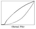
도 7은 종래의 PVA(Patterned Vertically Aligned) 모드 액정 표시 장치를 실측한 감마 곡선이고,7 is a gamma curve measured by a conventional patterned vertically aligned (PVA) mode liquid crystal display device.
도 8은 본 발명의 실시예에 따른 액정 표시 장치를 실측한 감마 곡선이다.8 is a gamma curve measured by the liquid crystal display according to the exemplary embodiment of the present invention.
110 : 절연 기판 121 : 게이트선110: insulated substrate 121: gate line
123 : 게이트 전극 131 : 유지 전극선123: gate electrode 131: sustain electrode line
140 : 게이트 절연막 171 : 데이터 선140: gate insulating film 171: data line
173 : 소스 전극 175a, 175b : 드레인 전극173:
174 : 결합 전극 180 : 보호막174: bonding electrode 180: protective film
190a, 190b : 화소 전극190a, 190b: pixel electrode
191, 192, 193 : 하측 절개부 271, 272, 273, 274 : 상측 절개부191, 192, 193:
본 발명은 액정 표시 장치 및 그에 사용되는 기판에 관한 것이다.The present invention relates to a liquid crystal display device and a substrate used therein.
액정 표시 장치는 일반적으로 공통 전극과 컬러 필터(color filter) 등이 형성되어 있는 상부 기판과 박막 트랜지스터와 화소 전극 등이 형성되어 있는 하부 기판 사이에 액정 물질을 주입해 놓고 화소 전극과 공통 전극에 서로 다른 전압을 인가함으로써 전계를 형성하여 액정 분자들의 배열을 변경시키고, 이를 통해 빛의 투과율을 조절함으로써 화상을 표현하는 장치이다.In general, a liquid crystal display device injects a liquid crystal material between an upper substrate on which a common electrode, a color filter, and the like are formed, and a lower substrate on which a thin film transistor and a pixel electrode are formed. By applying a different voltage to form an electric field to change the arrangement of the liquid crystal molecules, and through this to adjust the transmittance of light to represent the image.
그런데 액정 표시 장치는 시야각이 좁은 것이 중요한 단점이다. 이러한 단점을 극복하고자 시야각을 넓히기 위한 다양한 방안이 개발되고 있는데, 그 중에서도 액정 분자를 상하 기판에 대하여 수직으로 배향하고 화소 전극과 그 대향 전극인 공통 전극에 일정한 개구 패턴을 형성하거나 돌기를 형성하는 방법이 유력시되고 있다.However, it is an important disadvantage that the liquid crystal display device has a narrow viewing angle. In order to overcome these disadvantages, various methods for widening the viewing angle have been developed. Among them, liquid crystal molecules are oriented vertically with respect to the upper and lower substrates, and a method of forming a constant opening pattern or forming protrusions on the pixel electrode and the common electrode opposite thereto is performed. This is becoming potent.
개구 패턴을 형성하는 방법으로는 화소 전극과 공통 전극에 각각 개구 패턴을 형성하여 이들 개구 패턴으로 인하여 형성되는 프린지 필드(fringe field)를 이 용하여 액정 분자들이 눕는 방향을 조절함으로써 시야각을 넓히는 방법이 있다.As a method of forming the opening pattern, an opening pattern is formed in the pixel electrode and the common electrode, respectively, and a fringe field formed by the opening patterns is used to adjust the direction in which the liquid crystal molecules lie, thereby widening the viewing angle. .
돌기를 형성하는 방법은 상하 기판 위에 형성되어 있는 화소 전극과 공통 전극 위에 각각 돌기를 형성해 둠으로써 돌기에 의하여 왜곡되는 전기장을 이용하여 액정 분자의 눕는 방향을 조절하는 방식이다.The method of forming the protrusions is a method of controlling the lying direction of the liquid crystal molecules by using the electric field distorted by the protrusions by forming protrusions on the pixel electrode and the common electrode formed on the upper and lower substrates, respectively.
또 다른 방법으로는, 하부 기판 위에 형성되어 있는 화소 전극에는 개구 패턴을 형성하고 상부 기판에 형성되어 있는 공통 전극 위에는 돌기를 형성하여 개구 패턴과 돌기에 의하여 형성되는 프린지 필드를 이용하여 액정의 눕는 방향을 조절함으로써 도메인을 형성하는 방식이 있다.In another method, an opening pattern is formed on the pixel electrode formed on the lower substrate, and a protrusion is formed on the common electrode formed on the upper substrate, so that the liquid crystal lies down using the fringe field formed by the opening pattern and the protrusion. There is a way to form a domain by controlling.
이러한 다중 도메인 액정 표시 장치는 1:10의 대비비를 기준으로 하는 대비비 기준 시야각이나 계조간의 휘도 반전의 한계 각도로 정의되는 계조 반전 기준 시야각은 전 방향 80°이상으로 매우 우수하다. 그러나 정면의 감마(gamma)곡선과 측면의 감마 곡선이 일치하지 않는 측면 감마 곡선 왜곡 현상이 발생하여 TN(twisted nematic) 모드 액정 표시 장치에 비하여도 좌우측면에서 열등한 시인성을 나타낸다. 예를 들어, 도메인 분할 수단으로 개구부를 형성하는 PVA(patterned vertically aligned) 모드의 경우에는 측면으로 갈수록 전체적으로 화면이 밝게 보이고 색은 흰색 쪽으로 이동하는 경향이 있으며, 심한 경우에는 밝은 계조 사이의 간격 차이가 없어져서 그림이 뭉그러져 보이는 경우도 발생한다. 그런데 최근 액정 표시 장치가 멀티 미디어용으로 사용되면서 그림을 보거나 동영상을 보는 일이 증가하면서 시인성이 점점 더 중요시되고 있다.In such a multi-domain liquid crystal display, the gray scale inversion reference viewing angle defined as a contrast ratio reference viewing angle based on a contrast ratio of 1:10 or a limit angle of luminance inversion between gray scales is excellent, more than 80 ° in all directions. However, the gamma curve of the front side and the gamma curve of the side do not coincide with each other, resulting in inferior visibility in the left and right sides compared to the TN (twisted nematic) mode liquid crystal display. For example, in the patterned vertically aligned (PVA) mode in which openings are formed by domain dividing means, the screen looks brighter toward the side and the color tends to shift toward white. Occasionally, the picture appears clumped and disappears. However, as liquid crystal display devices are used for multimedia in recent years, visibility has become increasingly important as pictures and moving pictures are viewed.
본 발명이 이루고자 하는 기술적 과제는 시인성이 우수한 다중 도메인 액정 표시 장치를 구현하는 것이다. The technical problem to be achieved by the present invention is to implement a multi-domain liquid crystal display device having excellent visibility.
이러한 과제를 해결하기 위하여 본 발명에서는 제1 절연 기판, 상기 제1 절연 기판 위에 제1 방향으로 형성되어 있는 제1 신호선, 상기 제1 절연 기판 위에 제2 방향으로 형성되어 있으며 상기 제1 신호선과 절연되어 교차하고 있는 제2 신호선, 상기 제1 신호선 및 상기 제2 신호선에 연결되어 있는 제1 박막 트랜지스터, 상기 제1 박막 트랜지스터가 연결되어 있는 상기 제1 신호선 및 상기 제2 신호선에 연결되어 있는 제2 박막 트랜지스터, 상기 제1 박막 트랜지스터에 연결되어 있는 제1 화소 전극, 상기 제2 박막 트랜지스터에 연결되어 있는 제2 화소 전극, 상기 제1 절연 기판과 대향하는 제2 절연 기판, 상기 제2 절연 기판 위에 형성되어 있는 기준 전극, 상기 제1 기판과 상기 제2 기판 사이에 주입되어 있는 액정 물질층, 상기 제1 절연 기판과 상기 제2 절연 기판 중의 적어도 어느 한 기판 위에 형성되어 있으며 상기 제1 화소 전극과 상기 제2 화소 전극을 다수의 소 도메인으로 분할하는 도메인 분할 수단을 포함하고, 상기 도메인 분할 수단은 상기 제1 화소 전극과 상기 제2 화소 전극을 각각 제1 방향 도메인과 제2 방향 도메인으로 분할하고, 상기 제1 및 제2 방향 도메인 내의 액정의 평균 방향자는 상기 제1 또는 제2 신호선과 0°보다 크고90°보다 작은 소정의 각도를 이루며, 상기 제1 화소 전극과 상기 제2 화소 전극은 서로 용량성 결합을 이루는 액정 표시 장치를 마련한다.In order to solve this problem, the present invention provides a first insulating substrate, a first signal line formed in a first direction on the first insulating substrate, and a second signal formed on the first insulating substrate in a second direction, and insulated from the first signal line. And a second signal line intersecting with each other, a first thin film transistor connected to the first signal line and the second signal line, a second signal line connected to the first signal line and the second signal line connected to the first thin film transistor. A thin film transistor, a first pixel electrode connected to the first thin film transistor, a second pixel electrode connected to the second thin film transistor, a second insulating substrate facing the first insulating substrate, and on the second insulating substrate A reference electrode formed, a liquid crystal material layer injected between the first substrate and the second substrate, the first insulating substrate and the second insulation A domain dividing means formed on at least one substrate of the plate and dividing the first pixel electrode and the second pixel electrode into a plurality of small domains, wherein the domain dividing means comprises the first pixel electrode and the second pixel; The pixel electrode is divided into a first direction domain and a second direction domain, respectively, and an average director of the liquid crystal in the first and second direction domains is a predetermined angle greater than 0 ° and less than 90 ° with the first or second signal line. A liquid crystal display device having a capacitive coupling between the first pixel electrode and the second pixel electrode is provided.
이 때, 상기 제1 화소 전극이 전체 화소 영역 면적의 50% 내지 80%를 차지하 는 것이 바람직하고, 액정 표시 장치의 구동시 상기 제1 화소 전극의 Vth 전압은 상기 제2 화소 전극의 Vth 전압보다 0.4V 내지 1.0V 낮은 것이 바람직하다. 또, 상기 박막 트랜지스터 기판에 형성되어 있으며 상기 제1 화소 전극 및 상기 제2 화소 전극과의 사이에서 각각 유지 용량을 형성하는 유지 전극선을 더 포함할 수 있고, 상기 제1 및 제2 방향 도메인 내의 액정의 평균 방향자는 상기 제1 또는 제2 신호선과 실질적으로 45°를 이루는 것이 좋다. 또한 상기 제1 기판 외측에 배치되어 있으며 편광축이 상기 제1 신호선 또는 제2 신호선과 나란한 제1 편광판과 상기 제2 기판 외측에 배치되어 있으며 편광축이 상기 제1 편광판과 수직을 이루는 제2 편광판을 더 포함할 수 있다.In this case, it is preferable that the first pixel electrode occupies 50% to 80% of the total pixel area area, and the Vth voltage of the first pixel electrode is Vth voltage of the second pixel electrode when the liquid crystal display is driven. It is preferable that it is 0.4-1.0V lower than. The liquid crystal display may further include a storage electrode line formed on the thin film transistor substrate and forming a storage capacitor between the first pixel electrode and the second pixel electrode, respectively, and the liquid crystal in the first and second directional domains. The average director of may be substantially 45 degrees with the first or second signal line. Further, a first polarizing plate disposed outside the first substrate and having a polarization axis parallel to the first signal line or a second signal line, and a second polarizing plate disposed outside the second substrate and having a polarization axis perpendicular to the first polarizing plate. It may include.
더욱 구체적으로는, 절연 기판, 상기 기판 위에 형성되어 있으며 게이트선 및 게이트 전극을 포함하는 게이트 배선, 상기 게이트선 위에 형성되어 있는 게이트 절연막, 상기 게이트 절연막 위에 형성되어 있는 반도체층, 상기 반도체층 및 상기 게이트 절연막 위에 형성되어 있으며 상기 게이트선과 교차하는 데이터선, 소스 전극, 제1 및 제2 드레인 전극을 포함하는 데이터 배선, 상기 게이트 절연막 위의 상기 데이터선과 상기 게이트선이 교차하여 정의하는 화소 영역마다 형성되어 있는 결합 전극, 상기 데이터 배선 위에 형성되어 있으며 상기 제1 및 제2 드레인 전극과 상기 결합 전극을 각각 노출하는 접촉구를 가지는 보호막, 상기 보호막 위에 형성되어 있으며 상기 제1 드레인 전극 및 상기 결합 전극과 연결되어 있는 제1 화소 전극, 상기 보호막 위에 형성되어 있으며 상기 제2 드레인 전극과 연결되어 있고 상기 결합 전극과 일부가 중첩되어 있는 제2 화소 전극을 포함하고, 상기 제1 화소 전극과 상기 제2 화소 전극 중의 적어도 하나는 사선 방향 절개부를 가지는 박막 트랜지스터 기판을 마련한다.More specifically, an insulating substrate, a gate wiring formed on the substrate and including a gate line and a gate electrode, a gate insulating film formed on the gate line, a semiconductor layer formed on the gate insulating film, the semiconductor layer, and the A data line formed on the gate insulating layer and intersecting the gate line, a data line including a source electrode, a first and second drain electrodes, and a pixel area defined by the data line and the gate line on the gate insulating layer intersecting with each other. A coupling electrode formed on the data line, the passivation layer having a contact hole exposing the first and second drain electrodes and the coupling electrode, respectively, the passivation layer formed on the passivation layer, and the first drain electrode and the coupling electrode; A first pixel electrode connected on the passivation layer And a second pixel electrode formed to be connected to the second drain electrode and partially overlapping the coupling electrode, wherein at least one of the first pixel electrode and the second pixel electrode has a diagonal cutout. Prepare a transistor substrate.
또는, 절연 기판, 상기 기판 위에 형성되어 있으며 게이트선 및 게이트 전극을 포함하는 게이트 배선, 상기 게이트선 위에 형성되어 있는 게이트 절연막, 상기 게이트 절연막 위에 형성되어 있는 반도체층, 상기 반도체층 및 상기 게이트 절연막 위에 형성되어 있으며 상기 게이트선과 교차하는 데이터선, 소스 전극, 제1 및 제2 드레인 전극을 포함하는 데이터 배선, 상기 게이트 절연막 위의 상기 데이터선과 상기 게이트선이 교차하여 정의하는 화소 영역마다 형성되어 있는 결합 전극, 상기 데이터 배선 위에 형성되어 있으며 상기 제1 및 제2 드레인 전극과 상기 결합 전극을 각각 노출하는 접촉구를 가지는 보호막, 상기 보호막 위에 형성되어 있으며 상기 제1 드레인 전극 및 상기 결합 전극과 연결되어 있는 제1 화소 전극, 상기 보호막 위에 형성되어 있으며 상기 제2 드레인 전극과 연결되어 있고 상기 결합 전극과 일부가 중첩되어 있는 제2 화소 전극, 상기 제1 절연 기판과 대향하는 제2 절연 기판, 상기 제2 절연 기판 위에 형성되어 있는 기준 전극, 상기 제1 절연 기판과 상기 제2 절연 기판 중의 적어도 하나의 위에 형성되어 있는 도메인 분할 수단, 상기 제1 절연 기판과 상기 제2 절연 기판 사이에 주입되어 있는 액정 물질을 포함하고, 상기 도메인 분할 수단에 의하여 분할되는 각 도메인의 가장 긴 두 변은 상기 게이트선 또는 상기 데이터선에 대하여 실질적으로 45°를 이루는 액정 표시 장치를 마련한다.Or an insulating substrate, a gate wiring formed on the substrate and including a gate line and a gate electrode, a gate insulating film formed on the gate line, a semiconductor layer formed on the gate insulating film, on the semiconductor layer and the gate insulating film A data line, a data line including a data line, a source electrode, and first and second drain electrodes intersecting the gate line, and a coupling formed in each pixel region defined by the data line and the gate line on the gate insulating layer intersecting with each other. An electrode, a passivation layer formed on the data line and having contact holes exposing the first and second drain electrodes and the coupling electrode, respectively, and formed on the passivation layer and connected to the first drain electrode and the coupling electrode. A first pixel electrode formed on the passivation layer And a second pixel electrode connected to the second drain electrode and partially overlapping with the coupling electrode, a second insulating substrate facing the first insulating substrate, and a reference electrode formed on the second insulating substrate. Domain dividing means formed on at least one of the first insulating substrate and the second insulating substrate, and a liquid crystal material injected between the first insulating substrate and the second insulating substrate, wherein the domain dividing means Two longest sides of each of the divided domains provide a liquid crystal display that is substantially 45 ° with respect to the gate line or the data line.
이 때, 상기 제1 화소 전극이 전체 화소 영역 면적의 50% 내지 80%를 차지하 는 것이 바람직하고, 액정 표시 장치의 구동시 상기 제1 화소 전극의 Vth 전압은 상기 제2 화소 전극의 Vth 전압보다 0.4V 내지 1.0V 낮은 것이 바람직하다.
In this case, it is preferable that the first pixel electrode occupies 50% to 80% of the total pixel area area, and the Vth voltage of the first pixel electrode is Vth voltage of the second pixel electrode when the liquid crystal display is driven. It is preferable that it is 0.4-1.0V lower than.
그러면 도면을 참고로 하여 본 발명의 실시예에 따른 액정 표시 장치에 대하여 설명한다.Next, a liquid crystal display according to an exemplary embodiment of the present invention will be described with reference to the drawings.
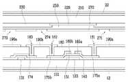
도 1은 본 발명의 실시예에 따른 액정 표시 장치의 배치도이고, 도 2는 도 1의 II-II'선에 대한 단면도이다.1 is a layout view of a liquid crystal display according to an exemplary embodiment of the present invention, and FIG. 2 is a cross-sectional view taken along line II-II 'of FIG. 1.
본 발명의 실시예에 따른 액정 표시 장치는 서로 대향하고 있는 박막 트랜지스터 기판과 색 필터 기판 및 그 사이에 주입되어 있는 액정층으로 이루어진다. 박막 트랜지스터 기판에는 박막 트랜지스터와 절개부를 가지는 화소 전극이 매트릭스 모양으로 반복 배치되어 있고, 색 필터 기판에는 색 필터와 절개부를 가지는 기준 전극이 형성되어 있다. 액정층의 액정 분자는 전계가 인가되지 않은 상태에서 두 기판에 대하여 수직으로 이루도록 배향되어 있다. 이하에서는 이들 각각에 대하여 좀더 구체적으로 살펴본다.The liquid crystal display according to the exemplary embodiment of the present invention includes a thin film transistor substrate and a color filter substrate facing each other, and a liquid crystal layer injected therebetween. The thin film transistor and the pixel electrode having the cutout are repeatedly arranged in a matrix shape on the thin film transistor substrate, and the reference electrode having the color filter and the cutout is formed on the color filter substrate. The liquid crystal molecules of the liquid crystal layer are aligned so as to be perpendicular to the two substrates without an electric field applied thereto. Hereinafter, each of them will be described in more detail.
먼저 박막 트랜지스터 기판에 대하여 설명한다.First, the thin film transistor substrate will be described.
유리 등의 투명한 절연 기판(110) 위에 가로 방향으로 뻗어 있는 게이트선(121)이 형성되어 있고, 게이트선(121)의 일부는 게이트 전극(123)을 이룬다.A
또, 절연 기판(110) 위에는 유지 전극선(131)이 형성되어 있다. 유지 전극선(131)은 전체적으로 가로 방향으로 뻗어 있으나 부분적으로 굴곡을 이루고 있다.In addition, the
게이트 배선(121, 123)과 유지 전극선(131)의 위에는 게이트 절연막(140)이 형성되어 있고, 게이트 전극(123) 상부의 게이트 절연막(140) 위에는 비정질 규소층(151)이 형성되어 있다. 비정질 규소층(151)은 게이트 전극(123)과 중첩하여 박막 트랜지스터의 채널부를 이룬다. 비정질 규소층(151)의 위에는 인(P) 등의 N형 불순물이 고농도로 도핑되어 있는 비정질 규소로 이루어진 드레인부 저항성 접촉층(165a, 165b)이 형성되어 있다. 단면도에 나타나지는 않았으나 드레인부 저항성 접촉층(165a, 165b)과 마주하는 소스부 저항성 접촉층(163)이 형성되어 있다.A
저항성 접촉층(163, 165a, 165b) 및 게이트 절연막(140) 위에는 데이터 배선(171, 173, 175a, 175b) 및 결합 전극(174)이 형성되어 있다. 데이터 배선(171, 173, 175a, 175b)은 세로 방향으로 뻗어 있는 데이터선(171)과 그 일부분인 소스 전극(173) 및 이들과 분리되어 있는 제1 및 제2 드레인 전극(175a, 175b)을 포함한다. 소스 전극(173)은 게이트 전극(123) 상부에서 제1 및 제2 드레인 전극(175a, 175b)과 마주하고 있고, 제1 및 제2 드레인 전극(175a, 175b)의 한쪽 끝은 각각 게이트선(121)을 중심으로 하여 양쪽에 위치하는 제1 및 제2 화소 영역의 안쪽으로 뻗어 있다. 결합 전극(174)은 후술하는 바와 같이, 양쪽으로 분리되어 있는 제1 화소 전극(190a)과 제2 화소 전극(190b)을 전자기적으로 결합하고 있다. 여기에서, 저항성 접촉층(163, 165a, 165b)은 비정질 규소층(151)과 데이터 배선(171, 173, 175a, 175b)이 중첩하는 부분에만 형성되어 있다.The data lines 171, 173, 175a, and 175b and the
데이터 배선(171, 173, 175a, 175b)의 위에는 보호막(180)이 형성되어 있다. 이 때, 보호막(180)은 제1 및 제2 드레인 전극(171, 173, 175a, 175b)의 한쪽 끝을 각각 노출하는 제1 및 제2 접촉구(181, 182)와 결합 전극(174)의 한쪽 끝을 노출하는 제3 접촉구(183)를 가지고 있다.The
보호막(180)의 위에는 제1 접촉구(181)와 제2 접촉구(182)를 통하여 제1 드레인 전극(175a) 및 제2 드레인 전극(175b)과 각각 연결되어 있는 제1 및 제2 화소 전극(190a, 190b)이 형성되어 있다. 여기서 제2 화소 전극(190b)은 결합 전극(174)과 제3 접촉구(183)를 통하여 연결되어 있고, 제1 화소 전극(190a)은 결합 전극(174)과 중첩되어 있어서 전자기적으로 결합(용량성 결합)되어 있다. 결국, 제1 화소 전극(190a)과 제2 화소 전극(190b)은 결합 전극(174)을 매개로 하여 용량성 결합을 이루고 있다. 또한, 제1 및 제2 화소 전극(190a, 190b)은 유지 전극선(131)과 중첩하여 유지 용량을 형성한다. 제1 및 제2 화소 전극(190a, 190b)은 ITO(indium tin oxide) 또는 IZO(indium zinc oxide) 등의 투명한 도전 물질로 이루어진다. 한편, 제1 화소 전극(190a)은 제1 내지 제3 하측 절개부(191, 192, 193)를 가진다. 제3 하측 절개부(193)는 제1 화소 전극(190a)의 상하 중앙에 위치하며 좌에서 우로 파고 들어간 모양으로 형성되어 있고, 제1 및 제2 하측 절개부(191, 192)는 각각 제3 하측 절개부(193)에 의하여 상하로 구분된 제1 화소 전극(190a)의 상부 및 하부에 사선 방향으로 형성되어 있다. 제1 하측 절개부(191)와 제2 하측 절개부(192)는 제3 하측 절개부(193)를 중심으로 하여 서로 대칭을 이루고 있다. 제1 화소 전극(190a)과 제2 화소 전극(190b)이 인접하는 변은 V자 모양으로 꺾여 있다. 이 때, 제1 화소 전극(190a)의 변은 볼록한 V자이고 제2 화소 전극(190b)의 변은 오목한 V자이다.First and second pixel electrodes connected to the
다음 색필터 기판에 대하여 설명한다.Next, the color filter substrate will be described.
유리 등의 투명한 절연 기판(210) 위에 블랙 매트릭스(220)가 형성되어 있고, 블랙 매트릭스(220)에 의하여 정의되는 각 화소 영역에는 적, 녹, 청색의 색필터(230)가 반복적으로 형성되어 있다. 색필터(230) 위에는 오버코트막(250)이 형성되어 있고, 오버코트막(250)의 위에는 ITO 등의 투명한 도전 물질로 이루어진 기준 전극(270)이 형성되어 있다. 기준 전극(270)은 제1 내지 제4 상측 절개부(271, 272, 273, 274)를 가진다. 제1 내지 제3 상측 절개부(271, 272, 273)는 제1 화소 전극(190a)과 중첩하는 위치에 배치되어 제1 내지 제3 하측 절개부(191, 192, 193)와 함께 제1 화소 전극(190a)의 영역을 다수의 소도메인으로 분할하고 있고, 제4 상측 절개부(274)는 제2 화소 전극(190b)의 영역을 상하로 양분하여 4개의 소도메인으로 분할하고 있다.The
이 때, 하측 절개부(191, 192, 193)와 상측 절개부(271, 272, 273, 274)에 의하여 분할되는 각 소도메인은 실질적으로 4각형을 이루고, 그 장변 두 개는 게이트선(121)과 데이터선(171)에 대하여 약 45°를 이룬다.At this time, each of the small domains divided by the
두 기판(110, 210)의 바깥쪽에는 하부 및 상부 편광판(12, 22)이 부착되어 있다. 이 때, 이들 편광판(12, 22)의 편광축은 게이트선(121) 또는 데이터선(171)과 평행하고, 서로간에는 직교하도록 배치된다.Lower and
이러한 구조의 액정 표시 장치에서 제1 화소 전극(190a)과 제2 화소 전극(190b)은 서로 다른 박막 트랜지스터에 의하여 스위칭되므로 서로 다른 전압을 인가받을 수 있다. 또한 화소 행별로 위에서 아래로 순차적으로 구동하는 경우에 는 제1 화소 전극(190a)에 인가되는 전압이 제2 화소 전극(190b)에 인가되는 전압보다 일정 정도 낮게 유지된다. 따라서 각 계조에 따라 제1 화소 전극(190a)에 인가하는 전압은 제2 화소 전극(190b)에 인가하는 전압보다 일정 정도 낮게 설정[전압 쉬프트(shift)]되며, 이로 인하여 감마 곡선의 왜곡이 저감한다. 이 때, 제1 화소 전극(190a)과 제2 화소 전극(190b)의 면적비와 전압 쉬프트의 크기에 의하여 시인성이 크게 달라진다. 따라서 이들 값을 결정함에 있어 신중하여야 한다.In the liquid crystal display of the structure, the
그러면 제1 화소 전극(190a)의 전압이 제2 화소 전극(190b)의 전압보다 낮게 유지되는 이유를 도 3을 참고로 하여 설명한다.Next, the reason why the voltage of the
하나의 화소 영역 내에 배치되어 있는 두 화소 전극[P(n)-a, P(n)-b] 전압{V[P(n)-a], V[P(n)-b)]} 사이의 관계를 도출한다.Between two pixel electrodes P (n) -a, P (n) -b] voltages {V [P (n) -a], V [P (n) -b)] disposed in one pixel region To derive the relationship.
도 3에서 Clca는 a 화소 전극과 기준 전극 사이에서 형성되는 액정 용량, Csta는 유지 전극선과 a 화소 전극 사이에서 형성되는 유지 용량, Clcb는 b 화소 전극과 기준 전극 사이에서 형성되는 액정 용량, Cstb는 유지 전극선과 b 화소 전극 사이에서 형성되는 유지 용량, Cpp는 a 화소 전극과 b 화소 전극 사이에서 형성되는 결합 용량을 나타낸다.In FIG. 3, Clca is a liquid crystal capacitor formed between a pixel electrode and a reference electrode, Csta is a storage capacitor formed between a sustain electrode line and a pixel electrode, Clcb is a liquid crystal capacitor formed between a b pixel electrode and a reference electrode, and Cstb is The storage capacitor formed between the storage electrode line and the b pixel electrode, Cpp, represents the coupling capacitance formed between the a pixel electrode and the b pixel electrode.
도 3을 보면 동일한 게이트선과 데이터선에 제1 및 제2 박막 트랜지스터가 연결되어 있고, 제1 및 제2 박막 트랜지스터에는 각각 제1 화소 전극과 제2 화소 전극이 연결되어 있다. 유지 전극선(131)을 사이에 두고 있는 제1 화소 전극과 제2 화소 전극은 서로 용량성 결합(Cpp)을 이루고 있다.3, the first and second thin film transistors are connected to the same gate line and the data line, and the first pixel electrode and the second pixel electrode are connected to the first and second thin film transistors, respectively. The first pixel electrode and the second pixel electrode having the
하나의 데이터선(171)을 기준으로 볼 때, n 번째 게이트선(121)이 온(on)되 면 두 개의 박막 트랜지스터(TFT) 채널이 온되고 이를 통하여 제1 및 제2 화소 전극[P(n)-a, P(n)-b]에 전압이 인가된다. 그런데 P(n)-b는 P(n+1)-a와 용량성으로 결합되어 있어서 P(n+1)-a가 온될 때 P(n)-b가 영향을 받는다. 따라서 P(n)-a,와 P(n)-b의 전압은 다음과 같이 주어진다.Based on one

수학식 1 및 2에서 Vd(n)은 P(n) 화소를 구동하기 위하여 데이터선에 인가되는 전압을 의미하고, Vd(n+1)은 P(n+1)를 구동하기 위하여 인가된 데이터선 전압을 의미한다. 또, V'd(n+1)은 이전 프레임(frame)의 P(n+1) 화소에 인가되었던 전압을 의미한다.In
수학식 1 및 2에 나타낸 바와 같이, P(n)-b 화소에 인가되는 전압과 P(n)-a에 인가되는 전압은 서로 다르다. 특히, 점 반전 구동 또는 선 반전 구동을 하고, 다음 화소 행이 이전 화소 행과 동일한 계조를 표시하는 경우(실제로 대부분의 화소가 이러한 경우에 해당하는 시간이 많다.)에는 Vd(n)=-Vd(n+1), Vd(n)=-V'd(n)(기준 전극 전압은 접지 전압으로 가정함)이므로 수학식 2는 다음과 같이 정리할 수 있다.As shown in


수학식 3에 의하면, P(n)-b에는 P(n)-a보다 낮은 전압이 인가된다. 따라서 P(n+1) 화소가 P(n) 화소와 동일한 계조를 표시하는 경우에는 P(n+1)-a(제2 화소 전극에 해당)에 인가되는 전압이 P(n)-b(제1 화소 전극에 해당)에 인가되는 전압보다 높게된다.According to Equation 3, a voltage lower than P (n) -a is applied to P (n) -b. Therefore, when the P (n + 1) pixel displays the same gray level as the P (n) pixel, the voltage applied to P (n + 1) -a (corresponding to the second pixel electrode) is P (n) -b ( The voltage applied to the first pixel electrode).
도 4는 전압 쉬프트와 도메인 비율에 따른 시인성 왜곡량을 나타내는 그래프이다.4 is a graph showing visibility distortion amount according to voltage shift and domain ratio.
도 4에서 세로축은 시인성 왜곡량을 정량화한 값이고, 가로축은 제1 화소 전극(190a)과 제2 화소 전극(190b)의 면적비와 전압 쉬프트의 크기를 나타낸다.In FIG. 4, the vertical axis indicates the amount of visibility distortion, and the horizontal axis indicates the area ratio of the
시인성 왜곡량이 0.1~0.2 이면 CRT(cathode ray tube) 수준의 극히 우수한 시인성을 나타냄을 의미하고, 0.2~0.25 이면 매우 우수한 시인성을 나타내는 것이고, 0.25~0.3이면 시인성이 우수한 편이며, 0.3~0.35이면 양호한 정도이다. 0.35 이하는 시인성이 열등하여 표시 품질이 좋지 못하다.Visibility of 0.1 ~ 0.2 means very good visibility at the level of cathode ray tube (CRT), 0.2 ~ 0.25 indicates very good visibility, 0.25 ~ 0.3 is good visibility, and 0.3 ~ 0.35 is good. It is enough. Less than 0.35 is inferior in visibility and the display quality is not good.
도 4를 바탕으로 하여 판단할 때, 제1 화소 전극과 제2 화소 전극의 면적비가 50:50 ~ 80:20일 때 우수한 시인성을 나타내고, 전압 쉬프트량은 Vth 부근에서 0.4에서 1.0V 일 때 우수한 시인성을 나타낸다. 즉, 제1 화소 전극을 제2 화소 전극에 비하여 크게 설계하는 것이 바람직하다. 그러나 킥백(kick-back) 전압 등의 문제로 인하여 제1 화소 전극이 제2 화소 전극보다 80% 이상이 되면 플리커(flicker) 등의 다양한 문제가 발생하여 바람직하지 못하다. 또, 제1 화소 전극의 Vth 전압이 제2 화소 전극의 Vth 전압보다 0.4V~1.0V 낮게 되면 시인성이 향상된다. 제1 화소 전극과 제2 화소 전극의 전압차는 고계조로 가면 더 커질 수 있다.Judging from FIG. 4, excellent visibility is seen when the area ratio of the first pixel electrode and the second pixel electrode is 50:50 to 80:20, and the voltage shift amount is excellent when 0.4 to 1.0V near Vth. It shows visibility. In other words, it is preferable to design the first pixel electrode larger than the second pixel electrode. However, when the first pixel electrode is 80% or more than the second pixel electrode due to a problem such as a kick-back voltage, various problems such as flicker may occur, which is not preferable. In addition, the visibility is improved when the Vth voltage of the first pixel electrode is 0.4V to 1.0V lower than the Vth voltage of the second pixel electrode. The voltage difference between the first pixel electrode and the second pixel electrode may become larger when the gray level is high.
그러면 본 발명에 따른 액정 표시 장치에서 시인성이 개선되는 이유를 도 5와 도 6을 참고로 하여 설명한다.Next, the reason why the visibility is improved in the liquid crystal display according to the present invention will be described with reference to FIGS. 5 and 6.
도 5는 종래의 액정 표시 장치의 측면에서의 감마 곡선 왜곡을 나타내는 그래프이고, 도 6은 본 발명에 의하여 측면에서의 감마 곡선 왜곡이 감소하는 것을 나타내는 그래프이다.FIG. 5 is a graph showing gamma curve distortion at the side of a conventional liquid crystal display, and FIG. 6 is a graph showing the reduction of gamma curve distortion at the side according to the present invention.
도 5를 보면, 종래와 같이 하나의 화소 전극만을 형성하는 경우에는 정면 감마 곡선에 비하여 측면의 감마 곡선이 위쪽으로 크게 왜곡됨을 알 수 있다. 그러나 본 발명과 같이, 화소 전극을 두 개의 서브 전극(제1 화소 전극 및 제2 화소 전극)으로 나누고, 이들 두 서브 전극을 용량성으로 결합하면, 한쪽 서브 전극(제1 화소 전극)에 인가되는 전압이 쉬프트된다. 이 때, 제1 화소 전극에 인가하는 전압이 통상의 계조 전압보다 낮게 되도록 화상 신호 전압을 설정하면, 저계조의 소정 범위에서 제1 화소 전극의 전압이 문턱 전압(Vth) 이하로 유지되므로 제1 화소 전극 부분은 블랙 상태로 유지되고 제2 화소 전극 부분만이 휘도 증가에 기여하게 된다. 그런데 제2 화소 전극 부분의 면적이 작으므로 휘도 증가도 적다(도 6의 '제2 화소 전극만 on' 부분). 일정 계조 이상이 되면 제1 화소 전극의 전압도 문턱 전압 이상으로 올라가게 되므로 제1 화소 전극도 휘도 증가에 기여하게 되어 휘도 증가가 커진다(도 6의 '제1 화소 전극과 제2 화소 전극 on' 부분). 따라서, 도 6에 나타낸 바와 같이, 감마 곡선의 왜곡이 감소하게 된다.Referring to FIG. 5, it can be seen that when only one pixel electrode is formed as in the related art, the gamma curve of the side surface is greatly distorted upward compared to the front gamma curve. However, as in the present invention, when the pixel electrode is divided into two sub-electrodes (the first pixel electrode and the second pixel electrode), and these two sub-electrodes are capacitively coupled, they are applied to one sub-electrode (the first pixel electrode). The voltage is shifted. At this time, when the image signal voltage is set so that the voltage applied to the first pixel electrode is lower than the normal gray voltage, the voltage of the first pixel electrode is kept below the threshold voltage Vth in a predetermined range of low grayscale, so that the first The pixel electrode portion remains black and only the second pixel electrode portion contributes to the increase in luminance. However, since the area of the second pixel electrode portion is small, the luminance increase is also small (the 'only second pixel electrode on' portion of FIG. 6). When the gray level is higher than the predetermined gray level, the voltage of the first pixel electrode also rises above the threshold voltage, so that the first pixel electrode also contributes to the increase in brightness, thereby increasing the brightness ('first pixel electrode and second pixel electrode on' of FIG. 6). part). Therefore, as shown in Fig. 6, the distortion of the gamma curve is reduced.
도 7은 종래의 PVA(Patterned Vertically Aligned) 모드 액정 표시 장치를 실측한 감마 곡선이고, 도 8은 본 발명의 실시예에 따른 액정 표시 장치를 실측한 감마 곡선이다.FIG. 7 is a gamma curve obtained by measuring a conventionally patterned vertically aligned (PVA) mode liquid crystal display, and FIG. 8 is a gamma curve measured by a liquid crystal display according to an exemplary embodiment of the present invention.
도 7과 도 8을 비교하면 본 발명의 실시예에 따른 액정 표시 장치의 감마 곡선 왜곡이 모든 방향에서 종래의 액정 표시 장치에 비하여 적음을 알 수 있다.7 and 8 illustrate that the gamma curve distortion of the liquid crystal display according to the exemplary embodiment of the present invention is smaller than that of the conventional liquid crystal display in all directions.
본 발명에서는 하나의 화소 영역에 두 개의 화소 전극과 박막 트랜지스터를 배치하고, 이들 두 화소 전극을 용량성으로 결합시킴으로써 전방향에서의 시인성을 개선한다. 또한, 액정의 평균 방향자가 게이트선 또는 데이터선에 대하여 45°방향을 향하도록 도메인을 분할하기 때문에 편광축이 게이트선 또는 데이터선과 나란한 편광판을 사용할 수 있다. 따라서 편광판의 제작비용을 절감할 수 있다.In the present invention, two pixel electrodes and a thin film transistor are disposed in one pixel region, and the two pixel electrodes are capacitively coupled to improve visibility in all directions. Further, since the domain is divided so that the average director of the liquid crystal is directed toward the 45 ° direction with respect to the gate line or the data line, a polarizing plate in which the polarization axis is parallel to the gate line or the data line can be used. Therefore, the manufacturing cost of the polarizing plate can be reduced.
Claims (10)
Translated fromKoreanPriority Applications (18)
| Application Number | Priority Date | Filing Date | Title |
|---|---|---|---|
| KR1020020036979AKR100840326B1 (en) | 2002-06-28 | 2002-06-28 | Liquid crystal display device and thin film transistor substrate used therein |
| US10/602,710US6850302B2 (en) | 2002-06-28 | 2003-06-25 | Liquid crystal display and thin film transistor array panel therefor |
| TW092117649ATWI272427B (en) | 2002-06-28 | 2003-06-27 | Liquid crystal display and thin film transistor array panel therefor |
| CN201310104028.5ACN103217834B (en) | 2002-06-28 | 2003-06-28 | Liquid crystal display |
| CN2008101305054ACN101320184B (en) | 2002-06-28 | 2003-06-28 | Liquid crystal display and thin film transistor array panel therefor |
| CN2010102473425ACN101916020B (en) | 2002-06-28 | 2003-06-28 | LCD Monitor |
| CNB031588433ACN100412673C (en) | 2002-06-28 | 2003-06-28 | Liquid crystal display and thin film transistor array panel thereof |
| JP2003186142AJP4550379B2 (en) | 2002-06-28 | 2003-06-30 | Liquid crystal display device and thin film transistor substrate used therefor |
| US11/043,157US7280177B2 (en) | 2002-06-28 | 2005-01-27 | Liquid crystal display and thin film transistor array panel therefor |
| US11/845,438US8743331B2 (en) | 2002-06-28 | 2007-08-27 | Liquid crystal display and thin film transistor array panel therefor |
| JP2008290350AJP5517438B2 (en) | 2002-06-28 | 2008-11-12 | Liquid crystal display device and thin film transistor substrate used therefor |
| JP2010131531AJP5680343B2 (en) | 2002-06-28 | 2010-06-08 | Liquid crystal display device and thin film transistor substrate used therefor |
| US12/820,687US8310643B2 (en) | 2002-06-28 | 2010-06-22 | Liquid crystal display and thin film transistor array panel therefor |
| US13/655,651US8698990B2 (en) | 2002-06-28 | 2012-10-19 | Liquid crystal display and thin film transistor array panel therefor |
| US14/197,781US9477121B2 (en) | 2002-06-28 | 2014-03-05 | Liquid crystal display and thin film transistor array panel therefor |
| US15/333,857US10012875B2 (en) | 2002-06-28 | 2016-10-25 | Liquid crystal display and thin film transistor array panel therefor |
| US16/025,311US10620488B2 (en) | 2002-06-28 | 2018-07-02 | Liquid crystal display and thin film transistor array panel therefor |
| US16/846,484US10969635B2 (en) | 2002-06-28 | 2020-04-13 | Liquid crystal display and thin film transistor array panel therefor |
Applications Claiming Priority (1)
| Application Number | Priority Date | Filing Date | Title |
|---|---|---|---|
| KR1020020036979AKR100840326B1 (en) | 2002-06-28 | 2002-06-28 | Liquid crystal display device and thin film transistor substrate used therein |
Related Child Applications (1)
| Application Number | Title | Priority Date | Filing Date |
|---|---|---|---|
| KR1020080041971ADivisionKR100925473B1 (en) | 2008-05-06 | 2008-05-06 | Liquid crystal display |
Publications (2)
| Publication Number | Publication Date |
|---|---|
| KR20040001687A KR20040001687A (en) | 2004-01-07 |
| KR100840326B1true KR100840326B1 (en) | 2008-06-20 |
Family
ID=31713068
Family Applications (1)
| Application Number | Title | Priority Date | Filing Date |
|---|---|---|---|
| KR1020020036979AExpired - LifetimeKR100840326B1 (en) | 2002-06-28 | 2002-06-28 | Liquid crystal display device and thin film transistor substrate used therein |
Country Status (5)
| Country | Link |
|---|---|
| US (9) | US6850302B2 (en) |
| JP (3) | JP4550379B2 (en) |
| KR (1) | KR100840326B1 (en) |
| CN (4) | CN101320184B (en) |
| TW (1) | TWI272427B (en) |
Families Citing this family (111)
| Publication number | Priority date | Publication date | Assignee | Title |
|---|---|---|---|---|
| JP3872377B2 (en)* | 2002-04-30 | 2007-01-24 | インターナショナル・ビジネス・マシーンズ・コーポレーション | Image display device and image display device |
| JP4248306B2 (en)* | 2002-06-17 | 2009-04-02 | シャープ株式会社 | Liquid crystal display |
| KR100840326B1 (en) | 2002-06-28 | 2008-06-20 | 삼성전자주식회사 | Liquid crystal display device and thin film transistor substrate used therein |
| KR100925463B1 (en)* | 2003-02-17 | 2009-11-06 | 삼성전자주식회사 | Liquid crystal display |
| KR100984345B1 (en)* | 2003-05-30 | 2010-09-30 | 삼성전자주식회사 | Thin film transistor array panel and liquid crystal display including the same |
| KR20040105934A (en)* | 2003-06-10 | 2004-12-17 | 삼성전자주식회사 | Liquid crystal display having multi domain and panel for the same |
| KR101337260B1 (en)* | 2003-08-13 | 2013-12-05 | 삼성디스플레이 주식회사 | Multi-domain liquid crystal display and a thin film transistor substrate of the same |
| US7206048B2 (en)* | 2003-08-13 | 2007-04-17 | Samsung Electronics Co., Ltd. | Liquid crystal display and panel therefor |
| KR101026810B1 (en)* | 2003-12-30 | 2011-04-04 | 삼성전자주식회사 | Multidomain liquid crystal display |
| KR101189267B1 (en) | 2004-12-03 | 2012-10-09 | 삼성디스플레이 주식회사 | A thin film transistor array panel and a liquid crystal display |
| KR20050098631A (en)* | 2004-04-08 | 2005-10-12 | 삼성전자주식회사 | Liquid crystal display and panel for the same |
| US7573551B2 (en) | 2004-05-21 | 2009-08-11 | Sanyo Electric Co., Ltd. | Transflective liquid crystal display device and color liquid crystal display device |
| KR101112537B1 (en)* | 2004-06-03 | 2012-02-29 | 삼성전자주식회사 | Liquid crystal display having multi domain and panel for the same |
| KR101100877B1 (en)* | 2004-07-09 | 2012-01-02 | 삼성전자주식회사 | Multi-domain display device and display panel used for it |
| TWI379113B (en)* | 2004-07-07 | 2012-12-11 | Samsung Display Co Ltd | Array substrate, manufacturing method thereof and display device having the same |
| KR101100878B1 (en)* | 2004-07-07 | 2012-01-02 | 삼성전자주식회사 | Multi-domain liquid crystal display and display panel used therefor |
| KR101189266B1 (en) | 2004-09-24 | 2012-10-09 | 삼성디스플레이 주식회사 | Liquid crystal display |
| KR101018754B1 (en)* | 2004-10-04 | 2011-03-04 | 삼성전자주식회사 | Liquid Crystal Display and Image Signal Correction Method |
| TWI338796B (en)* | 2004-10-29 | 2011-03-11 | Chimei Innolux Corp | Multi-domain vertically alignmentliquid crystal display panel |
| KR101112543B1 (en)* | 2004-11-04 | 2012-03-13 | 삼성전자주식회사 | Multi-domain thin film transistor array panel |
| KR101133757B1 (en)* | 2004-11-25 | 2012-04-09 | 삼성전자주식회사 | Liquid crystal display |
| KR101197044B1 (en) | 2004-12-02 | 2012-11-06 | 삼성디스플레이 주식회사 | Liquid crystal display |
| KR101112544B1 (en)* | 2004-12-03 | 2012-03-13 | 삼성전자주식회사 | Thin film transistor array panel and method for manufacturing the same |
| TWI399598B (en)* | 2004-12-27 | 2013-06-21 | Samsung Display Co Ltd | Liquid crystal display |
| KR101156510B1 (en)* | 2004-12-30 | 2012-06-18 | 엘지디스플레이 주식회사 | In-plain switching liquid crystal display device |
| JP4829501B2 (en)* | 2005-01-06 | 2011-12-07 | シャープ株式会社 | Liquid crystal display |
| KR101232618B1 (en)* | 2005-01-17 | 2013-02-13 | 삼성디스플레이 주식회사 | Array substrate, and liquid crystal display panel and liquid crystal display device having the same |
| KR101133760B1 (en) | 2005-01-17 | 2012-04-09 | 삼성전자주식회사 | Thin film transistor array panel and liquid crystal display including the panel |
| US8049699B2 (en) | 2005-02-07 | 2011-11-01 | Samsung Electronics Co., Ltd. | Liquid crystal display apparatus having storage electrodes overlapping only some sub-pixels |
| KR20060090159A (en)* | 2005-02-07 | 2006-08-10 | 삼성전자주식회사 | Liquid crystal display |
| KR101240642B1 (en) | 2005-02-11 | 2013-03-08 | 삼성디스플레이 주식회사 | Liquid crystal display |
| KR101188601B1 (en) | 2005-04-13 | 2012-10-08 | 삼성디스플레이 주식회사 | Liquid crystal display |
| JP4675677B2 (en)* | 2005-05-26 | 2011-04-27 | シャープ株式会社 | Liquid crystal display device |
| KR101163622B1 (en)* | 2005-07-07 | 2012-07-09 | 삼성전자주식회사 | Thin Film Transistor substrate |
| KR101171180B1 (en) | 2005-07-15 | 2012-08-20 | 삼성전자주식회사 | Liquid crystal display |
| KR101230301B1 (en)* | 2005-07-19 | 2013-02-06 | 삼성디스플레이 주식회사 | Liquid crystal display and driving method thereof |
| KR101153942B1 (en)* | 2005-07-20 | 2012-06-08 | 삼성전자주식회사 | Liquid crystal display |
| JP4466606B2 (en)* | 2005-09-07 | 2010-05-26 | エプソンイメージングデバイス株式会社 | Electro-optical device and electronic apparatus |
| KR101230304B1 (en)* | 2005-09-07 | 2013-02-06 | 삼성디스플레이 주식회사 | Liquid crystal display |
| KR101152135B1 (en)* | 2005-09-12 | 2012-06-15 | 삼성전자주식회사 | Liquid crystal display and driving method thereof |
| KR20070051045A (en)* | 2005-11-14 | 2007-05-17 | 삼성전자주식회사 | Liquid crystal display |
| KR20070051037A (en)* | 2005-11-14 | 2007-05-17 | 삼성전자주식회사 | Liquid crystal display |
| JP2007140089A (en) | 2005-11-18 | 2007-06-07 | Hitachi Displays Ltd | Liquid crystal display |
| KR101247113B1 (en)* | 2005-11-22 | 2013-04-01 | 삼성디스플레이 주식회사 | Display apparatus |
| KR20070063172A (en)* | 2005-12-14 | 2007-06-19 | 삼성전자주식회사 | Liquid Crystal Display and Manufacturing Method Thereof |
| KR101257380B1 (en)* | 2006-04-04 | 2013-04-23 | 삼성디스플레이 주식회사 | Display Apparatus |
| TWI322401B (en)* | 2006-07-13 | 2010-03-21 | Au Optronics Corp | Liquid crystal display |
| US8144291B2 (en)* | 2006-07-20 | 2012-03-27 | Sharp Kabushiki Kaisha | Display device and production method thereof |
| TWI330746B (en)* | 2006-08-25 | 2010-09-21 | Au Optronics Corp | Liquid crystal display and operation method thereof |
| TWI336804B (en)* | 2006-08-25 | 2011-02-01 | Au Optronics Corp | Liquid crystal display and operation method thereof |
| KR101225588B1 (en)* | 2006-09-04 | 2013-01-24 | 삼성디스플레이 주식회사 | Array substrate and display panel having the same |
| TWI312580B (en)* | 2006-09-04 | 2009-07-21 | Taiwan Tft Lcd Associatio | A thin film transistor, manufacturing method of a active layer thereof and liquid crystal display |
| KR101304417B1 (en)* | 2006-11-14 | 2013-09-06 | 삼성디스플레이 주식회사 | Liquid crystal display |
| US7852446B2 (en)* | 2006-09-18 | 2010-12-14 | Samsung Electronics Co., Ltd. | Liquid crystal display and method of driving the same |
| KR20080028572A (en)* | 2006-09-27 | 2008-04-01 | 삼성전자주식회사 | Liquid crystal composition and liquid crystal display comprising the same |
| KR20080030244A (en)* | 2006-09-29 | 2008-04-04 | 삼성전자주식회사 | Liquid crystal display |
| TWI344025B (en)* | 2006-10-11 | 2011-06-21 | Chunghwa Picture Tubes Ltd | Pixel structure and repair method thereof |
| CN101183196B (en)* | 2006-11-13 | 2010-06-16 | 中华映管股份有限公司 | Pixel |
| TWI342428B (en)* | 2006-12-29 | 2011-05-21 | Chimei Innolux Corp | Mva liquid crystal display panel |
| KR101369883B1 (en)* | 2007-02-26 | 2014-03-25 | 삼성디스플레이 주식회사 | Liquid crystal display |
| KR101340054B1 (en)* | 2007-06-05 | 2013-12-11 | 삼성디스플레이 주식회사 | Display apparatus and method of driving the same |
| TWI575293B (en)* | 2007-07-20 | 2017-03-21 | 半導體能源研究所股份有限公司 | Liquid crystal display device |
| JP2009092912A (en) | 2007-10-09 | 2009-04-30 | Hitachi Displays Ltd | Liquid crystal display device |
| KR101427582B1 (en)* | 2007-12-12 | 2014-08-08 | 삼성디스플레이 주식회사 | Panel and liquid crystal display including the same |
| TWI408647B (en)* | 2008-01-04 | 2013-09-11 | Wintek Corp | Liquid crystal display device and pixel structure thereof |
| EP2083314A1 (en)* | 2008-01-24 | 2009-07-29 | TPO Displays Corp. | Liquid crystal display device |
| KR101381348B1 (en)* | 2008-02-14 | 2014-04-17 | 삼성디스플레이 주식회사 | Liquid crystal display |
| TWI382261B (en)* | 2008-05-30 | 2013-01-11 | Chimei Innolux Corp | Liquid crystal display panel and driving method thereof |
| KR101252091B1 (en)* | 2008-10-28 | 2013-04-12 | 엘지디스플레이 주식회사 | Liquid crystal display of horizontal electronic fieldapplying type |
| TWI355260B (en)* | 2008-11-21 | 2012-01-01 | Univ Yuan Ze | Remote sleeping quality detecting system and metho |
| KR101545639B1 (en)* | 2008-12-12 | 2015-08-20 | 삼성디스플레이 주식회사 | Display substrate, method of manufacturing the same, and liquid crystal display device having the same |
| TWI383231B (en)* | 2009-02-27 | 2013-01-21 | Hannstar Display Corp | Pixel structure and driving method thereof |
| CN101866087B (en)* | 2009-04-14 | 2012-03-21 | 群康科技(深圳)有限公司 | Sub-pixel structure and liquid crystal display panel |
| US20110137185A1 (en)* | 2009-05-21 | 2011-06-09 | Starr Life Sciences Corp. | Saddle Faced Small Animal Sensor Clip |
| US20120200481A1 (en)* | 2009-10-16 | 2012-08-09 | Sharp Kabushiki Kaisha | Liquid crystal display |
| CN102472939A (en)* | 2009-10-21 | 2012-05-23 | 夏普株式会社 | Liquid crystal display device circuit, liquid crystal display device board, and liquid crystal display device |
| TWI418904B (en)* | 2009-10-26 | 2013-12-11 | Au Optronics Corp | Pixel structure and display panel having the same |
| KR101695474B1 (en)* | 2009-10-28 | 2017-01-13 | 삼성디스플레이 주식회사 | Liquid crystal display |
| US8878832B2 (en) | 2009-12-14 | 2014-11-04 | Sharp Kabushiki Kaisha | Pixel circuit, display device, and method for driving display device |
| TWI392946B (en)* | 2009-12-18 | 2013-04-11 | Au Optronics Corp | Pixel structure |
| TWI408477B (en)* | 2009-12-30 | 2013-09-11 | Au Optronics Corp | Pixel array, and polymer stablized alignment liquid crystal display panel |
| JP5292320B2 (en)* | 2010-01-12 | 2013-09-18 | シャープ株式会社 | Liquid crystal display |
| TWI407222B (en) | 2010-07-20 | 2013-09-01 | Au Optronics Corp | Pixel array, polymer stablized alignment liquid crystal display panel, and pixel array driving method |
| CN101950108A (en)* | 2010-07-28 | 2011-01-19 | 深圳市华星光电技术有限公司 | Liquid crystal display (LCD) |
| JP5379099B2 (en)* | 2010-09-10 | 2013-12-25 | シャープ株式会社 | Liquid crystal display |
| TWI432856B (en)* | 2010-12-07 | 2014-04-01 | Au Optronics Corp | Pixel structure |
| US7999899B1 (en) | 2011-01-25 | 2011-08-16 | Hannstar Display Corp. | Fringe field switching liquid crystal display apparatus |
| US8189158B1 (en) | 2011-09-29 | 2012-05-29 | Hannstar Display Corp. | Fringe field switching liquid crystal display apparatus |
| KR101230317B1 (en)* | 2011-11-21 | 2013-02-06 | 삼성디스플레이 주식회사 | Liquid crystal display |
| KR101994974B1 (en)* | 2013-01-10 | 2019-07-02 | 삼성디스플레이 주식회사 | Thin film trannsistor array panel and manufacturing method thereof |
| CN103116238B (en)* | 2013-02-05 | 2015-09-09 | 北京京东方光电科技有限公司 | A kind of array base palte and display panels |
| CN103197480B (en)* | 2013-03-22 | 2015-07-01 | 京东方科技集团股份有限公司 | Array substrate and manufacture method thereof and display panel with same |
| US10298073B2 (en)* | 2013-04-12 | 2019-05-21 | Semiconductor Components Industries, Llc | Method and apparatus for controlling wireless induction power supply |
| KR102108505B1 (en)* | 2013-10-23 | 2020-05-08 | 삼성디스플레이 주식회사 | Thin film transistor substrate and liquid crystal display |
| KR102144060B1 (en) | 2013-11-25 | 2020-08-14 | 삼성디스플레이 주식회사 | Display device and driving circuit thereof |
| KR20150099651A (en)* | 2014-02-21 | 2015-09-01 | 삼성디스플레이 주식회사 | Liquid crystal display device |
| KR102167689B1 (en)* | 2014-04-11 | 2020-10-20 | 삼성디스플레이 주식회사 | Display panel and display device having the same |
| US9992436B2 (en) | 2014-08-04 | 2018-06-05 | Invisage Technologies, Inc. | Scaling down pixel sizes in image sensors |
| JP2016085308A (en)* | 2014-10-24 | 2016-05-19 | 株式会社ジャパンディスプレイ | Liquid crystal display device and substrate for display device |
| KR20160087031A (en)* | 2015-01-12 | 2016-07-21 | 삼성디스플레이 주식회사 | Curved liquid crystal display device and method of manufacturing the same |
| US9703151B2 (en) | 2015-03-04 | 2017-07-11 | Apple Inc. | Liquid crystal display with color motion blur compensation structures |
| US9798199B2 (en) | 2015-03-04 | 2017-10-24 | Apple Inc. | Liquid crystal display with color motion blur compensation structures |
| KR20160120839A (en)* | 2015-04-08 | 2016-10-19 | 삼성디스플레이 주식회사 | Liquid crystal display device |
| KR20170039793A (en)* | 2015-10-01 | 2017-04-12 | 삼성디스플레이 주식회사 | Liquid display device |
| TWI579825B (en)* | 2016-08-29 | 2017-04-21 | 友達光電股份有限公司 | Display panel and driving method thereof |
| JP7159536B2 (en)* | 2017-05-30 | 2022-10-25 | 凸版印刷株式会社 | liquid crystal display |
| CN108154863B (en)* | 2018-02-28 | 2019-09-17 | 深圳市华星光电技术有限公司 | Pixel-driving circuit, image element driving method and liquid crystal display device |
| CN108538854B (en)* | 2018-03-30 | 2021-04-06 | 京东方科技集团股份有限公司 | A thin film transistor structure and preparation method thereof, array substrate and display device |
| CN109859705A (en)* | 2019-01-30 | 2019-06-07 | 惠科股份有限公司 | Driving method, display panel and driving module |
| CN110109296A (en)* | 2019-04-12 | 2019-08-09 | 深圳市华星光电半导体显示技术有限公司 | A kind of array substrate and liquid crystal display device |
| CN111880342B (en)* | 2020-07-29 | 2022-09-27 | 北海惠科光电技术有限公司 | Display panel, manufacturing method of display panel and display device |
Citations (11)
| Publication number | Priority date | Publication date | Assignee | Title |
|---|---|---|---|---|
| JPH0519298A (en)* | 1990-11-06 | 1993-01-29 | Honeywell Inc | Flat panel back plane and manufacture thereof |
| KR970005638A (en)* | 1995-07-25 | 1997-02-19 | 요트.게.아.롤페즈 | Ink jet recording device |
| KR970005638B1 (en)* | 1991-10-14 | 1997-04-18 | 호시덴 가부시기가이샤 | Gradation liquid crystal display panel |
| KR19990036740A (en)* | 1997-10-01 | 1999-05-25 | 다카노 야스아키 | Vertically Aligned Liquid Crystal Display |
| KR100196202B1 (en)* | 1994-05-31 | 1999-06-15 | 모리시따 요오이 찌 | Liquid crystal display device with a plurality of subpixels |
| KR100218584B1 (en)* | 1994-09-21 | 1999-09-01 | 모리시타 요이찌 | Liquid crystal display device and driving method thereof |
| JPH11352490A (en)* | 1998-05-19 | 1999-12-24 | Samsung Electronics Co Ltd | Wide viewing angle LCD |
| KR20000011961A (en)* | 1998-07-24 | 2000-02-25 | 마찌다 가쯔히꼬 | Liquid crystal display device and method for producing the same |
| KR20000031955A (en)* | 1998-11-11 | 2000-06-05 | 구본준 | Multi-domain liquid crystal display device |
| US6313899B1 (en)* | 1999-08-05 | 2001-11-06 | Chi Mei Electronics Corporation | Homeotropic liquid crystal display with protrusions comprising additional electrodes |
| US6400440B1 (en)* | 1999-06-23 | 2002-06-04 | International Business Machines Corporation | Passive liquid crystal display having pre-tilt control structure and light absorbent material at a center |
Family Cites Families (105)
| Publication number | Priority date | Publication date | Assignee | Title |
|---|---|---|---|---|
| JP2516197B2 (en)* | 1985-08-23 | 1996-07-10 | 株式会社日立製作所 | Semiconductor element inspection method |
| US4878742A (en) | 1986-08-04 | 1989-11-07 | Canon Kabushiki Kaisha | Liquid crystal optical modulator |
| JPH02204727A (en)* | 1989-02-02 | 1990-08-14 | Sharp Corp | active matrix substrate |
| JPH032731A (en) | 1989-05-31 | 1991-01-09 | Toshiba Corp | Active matrix type liquid crystal display element |
| JP3119709B2 (en) | 1990-12-20 | 2000-12-25 | 旭硝子株式会社 | Liquid crystal display device and projection type liquid crystal display device |
| JP2669954B2 (en) | 1991-05-08 | 1997-10-29 | シャープ株式会社 | Active matrix display |
| JPH07119919B2 (en)* | 1991-05-15 | 1995-12-20 | インターナショナル・ビジネス・マシーンズ・コーポレイション | Liquid crystal display |
| US5473450A (en) | 1992-04-28 | 1995-12-05 | Sharp Kabushiki Kaisha | Liquid crystal display device with a polymer between liquid crystal regions |
| US5309264A (en) | 1992-04-30 | 1994-05-03 | International Business Machines Corporation | Liquid crystal displays having multi-domain cells |
| WO1994008331A1 (en)* | 1992-10-06 | 1994-04-14 | Panocorp Display Systems | Drive system and method for panel displays |
| US5302916A (en) | 1992-12-21 | 1994-04-12 | At&T Bell Laboratories | Wide range digital frequency detector |
| JP3108768B2 (en) | 1992-12-24 | 2000-11-13 | スタンレー電気株式会社 | TN liquid crystal display device |
| JPH06230414A (en) | 1993-01-29 | 1994-08-19 | Toshiba Corp | Liquid crystal display element |
| JPH06273798A (en) | 1993-03-23 | 1994-09-30 | Fujitsu Ltd | LCD display panel |
| JPH06301036A (en) | 1993-04-12 | 1994-10-28 | Sanyo Electric Co Ltd | Liquid crystal display device |
| US5579140A (en) | 1993-04-22 | 1996-11-26 | Sharp Kabushiki Kaisha | Multiple domain liquid crystal display element and a manufacturing method of the same |
| JP2975844B2 (en) | 1993-06-24 | 1999-11-10 | 三洋電機株式会社 | Liquid crystal display |
| JPH0713191A (en) | 1993-06-28 | 1995-01-17 | Casio Comput Co Ltd | Active matrix liquid crystal display device |
| JP2859093B2 (en) | 1993-06-28 | 1999-02-17 | 三洋電機株式会社 | Liquid crystal display |
| JPH0720469A (en) | 1993-06-29 | 1995-01-24 | Tokuo Koma | Liquid crystal display device |
| JP3234357B2 (en) | 1993-07-08 | 2001-12-04 | 三洋電機株式会社 | Liquid crystal display |
| US5777700A (en) | 1993-07-14 | 1998-07-07 | Nec Corporation | Liquid crystal display with improved viewing angle dependence |
| JP2590693B2 (en) | 1993-07-14 | 1997-03-12 | 日本電気株式会社 | Liquid crystal display |
| TW386169B (en) | 1993-07-27 | 2000-04-01 | Tokyo Shibaura Electric Co | Liquid crystal display apparatus |
| DE69413624T2 (en) | 1993-07-27 | 1999-05-06 | Sharp K.K., Osaka | Liquid crystal display device |
| JPH0764089A (en) | 1993-08-31 | 1995-03-10 | Sanyo Electric Co Ltd | Liquid crystal display device |
| JP3294689B2 (en) | 1993-11-09 | 2002-06-24 | 株式会社日立製作所 | Liquid crystal display |
| US6292242B1 (en) | 1993-12-15 | 2001-09-18 | Ois Optical Imaging Systems, Inc. | Normally white twisted nematic LCD with positive uniaxial and negative biaxial retarders |
| JPH07230097A (en) | 1994-02-18 | 1995-08-29 | Sanyo Electric Co Ltd | Liquid crystal display device |
| JPH07261199A (en) | 1994-03-24 | 1995-10-13 | Matsushita Electric Ind Co Ltd | Thin film transistor type liquid crystal display device |
| JP3005418B2 (en) | 1994-05-18 | 2000-01-31 | 三洋電機株式会社 | Liquid crystal display |
| JPH07311390A (en) | 1994-05-18 | 1995-11-28 | Sanyo Electric Co Ltd | Liquid crystal display device |
| JP3311184B2 (en)* | 1995-01-30 | 2002-08-05 | 松下電器産業株式会社 | Liquid crystal display |
| JPH086052A (en) | 1994-06-24 | 1996-01-12 | Dainippon Printing Co Ltd | Liquid crystal optical element |
| JPH0815714A (en) | 1994-06-28 | 1996-01-19 | Casio Comput Co Ltd | Liquid crystal display element |
| JPH0829812A (en) | 1994-07-19 | 1996-02-02 | Toshiba Corp | Liquid crystal display |
| JP3066255B2 (en) | 1994-08-31 | 2000-07-17 | 三洋電機株式会社 | Liquid crystal display |
| JP3011072B2 (en) | 1994-09-21 | 2000-02-21 | 松下電器産業株式会社 | Liquid crystal display |
| JP2943665B2 (en) | 1994-09-21 | 1999-08-30 | 松下電器産業株式会社 | Liquid crystal display |
| JP3081468B2 (en) | 1994-09-30 | 2000-08-28 | 三洋電機株式会社 | Liquid crystal display |
| JP2951853B2 (en) | 1994-09-30 | 1999-09-20 | 松下電器産業株式会社 | Liquid crystal display |
| TW295652B (en)* | 1994-10-24 | 1997-01-11 | Handotai Energy Kenkyusho Kk | |
| JPH08129180A (en) | 1994-11-01 | 1996-05-21 | Fujitsu Ltd | LCD display panel |
| JPH08179341A (en) | 1994-12-22 | 1996-07-12 | Matsushita Electric Ind Co Ltd | Liquid crystal display device and driving method thereof |
| JPH08179343A (en) | 1994-12-22 | 1996-07-12 | Matsushita Electric Ind Co Ltd | Liquid crystal display element |
| JP3448384B2 (en) | 1995-02-20 | 2003-09-22 | 三洋電機株式会社 | Liquid crystal display |
| JPH08220524A (en) | 1995-02-20 | 1996-08-30 | Sanyo Electric Co Ltd | Liquid crystal display device |
| JP3590688B2 (en) | 1995-04-05 | 2004-11-17 | インターナショナル・ビジネス・マシーンズ・コーポレーション | Method and system for constructing an installation plan object for installing an application |
| JPH08338995A (en) | 1995-06-12 | 1996-12-24 | Citizen Watch Co Ltd | Liquid crystal display panel and its production |
| US5796456A (en) | 1995-07-14 | 1998-08-18 | Nec Corporation | Liquid crystal display with optical negative uni-axial compensation layer |
| JPH0943610A (en) | 1995-07-28 | 1997-02-14 | Toshiba Corp | Liquid crystal display |
| JPH0954323A (en) | 1995-08-11 | 1997-02-25 | Toshiba Corp | Liquid crystal display element |
| JPH09155437A (en) | 1995-10-06 | 1997-06-17 | Nisshin Steel Co Ltd | Manufacture of hot rolled steel sheet |
| JPH09160061A (en) | 1995-12-08 | 1997-06-20 | Toshiba Corp | Liquid crystal display device |
| JP3592419B2 (en) | 1995-12-21 | 2004-11-24 | 富士通ディスプレイテクノロジーズ株式会社 | LCD panel |
| KR100234402B1 (en) | 1996-01-19 | 1999-12-15 | 윤종용 | Method for driving a Liquid Crystal Display device and LCD device |
| JPH09230982A (en) | 1996-02-21 | 1997-09-05 | Kokusai Electric Co Ltd | transceiver |
| JPH09230991A (en) | 1996-02-23 | 1997-09-05 | Fuji Xerox Co Ltd | Information processor |
| JP3516370B2 (en) | 1996-03-14 | 2004-04-05 | 株式会社日立製作所 | Display device, video game device, monitor device, and information processing device |
| JP2734444B2 (en) | 1996-03-22 | 1998-03-30 | 日本電気株式会社 | Liquid crystal display |
| US6069600A (en)* | 1996-03-28 | 2000-05-30 | Kabushiki Kaisha Toshiba | Active matrix type liquid crystal display |
| JP3406772B2 (en)* | 1996-03-28 | 2003-05-12 | 株式会社東芝 | Active matrix type liquid crystal display |
| JPH09325373A (en) | 1996-06-04 | 1997-12-16 | Stanley Electric Co Ltd | Liquid crystal display device and method of manufacturing the same |
| JP3317637B2 (en) | 1996-07-30 | 2002-08-26 | シャープ株式会社 | Liquid crystal display device substrate, method of manufacturing the same, and liquid crystal display device using the same |
| JPH1090708A (en) | 1996-09-17 | 1998-04-10 | Toshiba Corp | Liquid crystal display device |
| KR100209281B1 (en)* | 1996-10-16 | 1999-07-15 | 김영환 | Lcd and its fabrication method |
| US6011531A (en) | 1996-10-21 | 2000-01-04 | Xerox Corporation | Methods and applications of combining pixels to the gate and data lines for 2-D imaging and display arrays |
| US6104450A (en)* | 1996-11-07 | 2000-08-15 | Sharp Kabushiki Kaisha | Liquid crystal display device, and methods of manufacturing and driving same |
| JPH10197894A (en) | 1996-12-28 | 1998-07-31 | Casio Comput Co Ltd | Liquid crystal display device and method of driving liquid crystal display device |
| JP3092537B2 (en)* | 1997-01-24 | 2000-09-25 | 日本電気株式会社 | Liquid crystal display |
| JP3231261B2 (en) | 1997-03-26 | 2001-11-19 | 株式会社アドバンスト・ディスプレイ | Liquid crystal display element and liquid crystal display device using the same |
| JP3966614B2 (en) | 1997-05-29 | 2007-08-29 | 三星電子株式会社 | Wide viewing angle LCD |
| US6704083B1 (en) | 1997-05-30 | 2004-03-09 | Samsung Electronics, Co., Ltd. | Liquid crystal display including polarizing plate having polarizing directions neither parallel nor perpendicular to average alignment direction of molecules |
| TW509808B (en) | 1997-06-12 | 2002-11-11 | Sharp Kk | Liquid crystal display device |
| JPH11109335A (en)* | 1997-09-30 | 1999-04-23 | Sharp Corp | Liquid crystal display |
| JP3819561B2 (en) | 1997-10-01 | 2006-09-13 | 三洋電機株式会社 | Liquid crystal display |
| KR100309918B1 (en) | 1998-05-16 | 2001-12-17 | 윤종용 | Liquid crystal display having wide viewing angle and method for manufacturing the same |
| KR100283511B1 (en) | 1998-05-20 | 2001-03-02 | 윤종용 | Wide viewing angle liquid crystal display |
| US6335776B1 (en)* | 1998-05-30 | 2002-01-01 | Lg. Philips Lcd Co., Ltd. | Multi-domain liquid crystal display device having an auxiliary electrode formed on the same layer as the pixel electrode |
| US6879364B1 (en) | 1998-09-18 | 2005-04-12 | Fujitsu Display Technologies Corporation | Liquid crystal display apparatus having alignment control for brightness and response |
| KR100662059B1 (en)* | 1998-10-12 | 2006-12-27 | 샤프 가부시키가이샤 | Liquid crystal display and method for fabricating the same |
| GB2343012B (en)* | 1998-10-19 | 2003-05-28 | Lg Philips Lcd Co Ltd | A multi-domain liquid crystal display device |
| JP2000235371A (en) | 1999-02-15 | 2000-08-29 | Matsushita Electric Ind Co Ltd | Liquid crystal display with built-in peripheral drive circuit |
| US6531993B1 (en)* | 1999-03-05 | 2003-03-11 | Semiconductor Energy Laboratory Co., Ltd. | Active matrix type display device |
| US6266166B1 (en) | 1999-03-08 | 2001-07-24 | Dai Nippon Printing Co., Ltd. | Self-adhesive film for hologram formation, dry plate for photographing hologram, and method for image formation using the same |
| DE19925985A1 (en)* | 1999-06-08 | 2000-12-14 | Bosch Gmbh Robert | Liquid crystal display with changeable viewing angle has electrically driven individual image element zones; different zones of image element can be selected via different column lines |
| CN1133149C (en)* | 1999-08-12 | 2003-12-31 | 友达光电股份有限公司 | Driving method of liquid crystal display |
| TW480722B (en)* | 1999-10-12 | 2002-03-21 | Semiconductor Energy Lab | Manufacturing method of electro-optical device |
| JP2001109018A (en) | 1999-10-12 | 2001-04-20 | Matsushita Electric Ind Co Ltd | Liquid crystal display device and driving method thereof |
| JP2001184012A (en)* | 1999-10-12 | 2001-07-06 | Sharp Corp | Matrix type display device |
| JP2001330852A (en)* | 2000-05-22 | 2001-11-30 | Matsushita Electric Ind Co Ltd | Liquid crystal panel and image display device using the same |
| JP2002122887A (en) | 2000-06-12 | 2002-04-26 | Nec Corp | Liquid crystal display device and its manufacturing method |
| JP3804910B2 (en) | 2000-07-31 | 2006-08-02 | 株式会社日立製作所 | Liquid crystal display |
| JP3712637B2 (en)* | 2000-08-11 | 2005-11-02 | シャープ株式会社 | Liquid crystal display device and defect correcting method thereof |
| KR100720093B1 (en) | 2000-10-04 | 2007-05-18 | 삼성전자주식회사 | Liquid crystal display |
| JP4368515B2 (en) | 2000-10-31 | 2009-11-18 | シャープ株式会社 | LCD panel |
| JP4072332B2 (en)* | 2001-01-09 | 2008-04-09 | シャープ株式会社 | Liquid crystal display device and driving method thereof |
| KR100831229B1 (en)* | 2001-12-10 | 2008-05-22 | 삼성전자주식회사 | High opening ratio liquid crystal display device |
| JP4342200B2 (en)* | 2002-06-06 | 2009-10-14 | シャープ株式会社 | Liquid crystal display |
| KR100840326B1 (en) | 2002-06-28 | 2008-06-20 | 삼성전자주식회사 | Liquid crystal display device and thin film transistor substrate used therein |
| US6922183B2 (en)* | 2002-11-01 | 2005-07-26 | Chin-Lung Ting | Multi-domain vertical alignment liquid crystal display and driving method thereof |
| KR100900541B1 (en) | 2002-11-14 | 2009-06-02 | 삼성전자주식회사 | Thin film transistor substrate for liquid crystal display |
| KR100887669B1 (en)* | 2002-12-28 | 2009-03-11 | 엘지디스플레이 주식회사 | LCD and its manufacturing method |
| US7019805B2 (en)* | 2002-12-31 | 2006-03-28 | Lg.Philips Lcd Co., Ltd. | Liquid crystal display device having a multi-domain structure and a manufacturing method for the same |
| JP2005019298A (en) | 2003-06-27 | 2005-01-20 | Asahi Glass Co Ltd | Membrane / electrode assembly for polymer electrolyte fuel cells |
- 2002
- 2002-06-28KRKR1020020036979Apatent/KR100840326B1/ennot_activeExpired - Lifetime
- 2003
- 2003-06-25USUS10/602,710patent/US6850302B2/ennot_activeExpired - Lifetime
- 2003-06-27TWTW092117649Apatent/TWI272427B/ennot_activeIP Right Cessation
- 2003-06-28CNCN2008101305054Apatent/CN101320184B/ennot_activeExpired - Lifetime
- 2003-06-28CNCN2010102473425Apatent/CN101916020B/ennot_activeExpired - Lifetime
- 2003-06-28CNCNB031588433Apatent/CN100412673C/ennot_activeExpired - Lifetime
- 2003-06-28CNCN201310104028.5Apatent/CN103217834B/ennot_activeExpired - Lifetime
- 2003-06-30JPJP2003186142Apatent/JP4550379B2/ennot_activeExpired - Lifetime
- 2005
- 2005-01-27USUS11/043,157patent/US7280177B2/ennot_activeExpired - Lifetime
- 2007
- 2007-08-27USUS11/845,438patent/US8743331B2/enactiveActive
- 2008
- 2008-11-12JPJP2008290350Apatent/JP5517438B2/ennot_activeExpired - Lifetime
- 2010
- 2010-06-08JPJP2010131531Apatent/JP5680343B2/ennot_activeExpired - Lifetime
- 2010-06-22USUS12/820,687patent/US8310643B2/ennot_activeExpired - Fee Related
- 2012
- 2012-10-19USUS13/655,651patent/US8698990B2/ennot_activeExpired - Lifetime
- 2014
- 2014-03-05USUS14/197,781patent/US9477121B2/ennot_activeExpired - Fee Related
- 2016
- 2016-10-25USUS15/333,857patent/US10012875B2/ennot_activeExpired - Lifetime
- 2018
- 2018-07-02USUS16/025,311patent/US10620488B2/ennot_activeExpired - Fee Related
- 2020
- 2020-04-13USUS16/846,484patent/US10969635B2/ennot_activeExpired - Fee Related
Patent Citations (11)
| Publication number | Priority date | Publication date | Assignee | Title |
|---|---|---|---|---|
| JPH0519298A (en)* | 1990-11-06 | 1993-01-29 | Honeywell Inc | Flat panel back plane and manufacture thereof |
| KR970005638B1 (en)* | 1991-10-14 | 1997-04-18 | 호시덴 가부시기가이샤 | Gradation liquid crystal display panel |
| KR100196202B1 (en)* | 1994-05-31 | 1999-06-15 | 모리시따 요오이 찌 | Liquid crystal display device with a plurality of subpixels |
| KR100218584B1 (en)* | 1994-09-21 | 1999-09-01 | 모리시타 요이찌 | Liquid crystal display device and driving method thereof |
| KR970005638A (en)* | 1995-07-25 | 1997-02-19 | 요트.게.아.롤페즈 | Ink jet recording device |
| KR19990036740A (en)* | 1997-10-01 | 1999-05-25 | 다카노 야스아키 | Vertically Aligned Liquid Crystal Display |
| JPH11352490A (en)* | 1998-05-19 | 1999-12-24 | Samsung Electronics Co Ltd | Wide viewing angle LCD |
| KR20000011961A (en)* | 1998-07-24 | 2000-02-25 | 마찌다 가쯔히꼬 | Liquid crystal display device and method for producing the same |
| KR20000031955A (en)* | 1998-11-11 | 2000-06-05 | 구본준 | Multi-domain liquid crystal display device |
| US6400440B1 (en)* | 1999-06-23 | 2002-06-04 | International Business Machines Corporation | Passive liquid crystal display having pre-tilt control structure and light absorbent material at a center |
| US6313899B1 (en)* | 1999-08-05 | 2001-11-06 | Chi Mei Electronics Corporation | Homeotropic liquid crystal display with protrusions comprising additional electrodes |
Also Published As
| Publication number | Publication date |
|---|---|
| US20050122457A1 (en) | 2005-06-09 |
| US9477121B2 (en) | 2016-10-25 |
| US8310643B2 (en) | 2012-11-13 |
| CN101916020A (en) | 2010-12-15 |
| US20200241367A1 (en) | 2020-07-30 |
| TWI272427B (en) | 2007-02-01 |
| KR20040001687A (en) | 2004-01-07 |
| JP5517438B2 (en) | 2014-06-11 |
| US20140184993A1 (en) | 2014-07-03 |
| CN103217834B (en) | 2016-06-08 |
| US20180307106A1 (en) | 2018-10-25 |
| CN101320184B (en) | 2013-07-10 |
| JP2010191476A (en) | 2010-09-02 |
| US6850302B2 (en) | 2005-02-01 |
| CN1495476A (en) | 2004-05-12 |
| JP2004038165A (en) | 2004-02-05 |
| TW200407627A (en) | 2004-05-16 |
| US20100259703A1 (en) | 2010-10-14 |
| US8698990B2 (en) | 2014-04-15 |
| CN103217834A (en) | 2013-07-24 |
| US20070285589A1 (en) | 2007-12-13 |
| CN101916020B (en) | 2012-05-02 |
| US20040070713A1 (en) | 2004-04-15 |
| US20170038646A1 (en) | 2017-02-09 |
| US10012875B2 (en) | 2018-07-03 |
| JP5680343B2 (en) | 2015-03-04 |
| US20130038808A1 (en) | 2013-02-14 |
| US10969635B2 (en) | 2021-04-06 |
| CN100412673C (en) | 2008-08-20 |
| US7280177B2 (en) | 2007-10-09 |
| CN101320184A (en) | 2008-12-10 |
| US8743331B2 (en) | 2014-06-03 |
| JP2009053718A (en) | 2009-03-12 |
| JP4550379B2 (en) | 2010-09-22 |
| US10620488B2 (en) | 2020-04-14 |
Similar Documents
| Publication | Publication Date | Title |
|---|---|---|
| KR100840326B1 (en) | Liquid crystal display device and thin film transistor substrate used therein | |
| CN1491371B (en) | Thin film transistor array panel for liquid crystal display | |
| JP5345188B2 (en) | Flat panel display | |
| US8279385B2 (en) | Liquid crystal display | |
| KR101702105B1 (en) | Liquid crystal display and driving method thereof | |
| US8259278B2 (en) | Liquid crystal display | |
| KR20080022920A (en) | LCD Display | |
| KR101189267B1 (en) | A thin film transistor array panel and a liquid crystal display | |
| KR101310309B1 (en) | Display panel | |
| KR101327300B1 (en) | Array substrate and display panel having the same | |
| KR20130042242A (en) | Liquid crystal display | |
| KR100840312B1 (en) | Thin film transistor substrate for liquid crystal display | |
| KR100925473B1 (en) | Liquid crystal display | |
| KR100968572B1 (en) | Liquid crystal display | |
| KR101367744B1 (en) | Liquid crystal display | |
| KR101261612B1 (en) | Liquid crystal display | |
| KR20100030646A (en) | Liquid crystal display | |
| KR100895317B1 (en) | Liquid crystal display |
Legal Events
| Date | Code | Title | Description |
|---|---|---|---|
| PA0109 | Patent application | Patent event code:PA01091R01D Comment text:Patent Application Patent event date:20020628 | |
| PG1501 | Laying open of application | ||
| A201 | Request for examination | ||
| PA0201 | Request for examination | Patent event code:PA02012R01D Patent event date:20070628 Comment text:Request for Examination of Application Patent event code:PA02011R01I Patent event date:20020628 Comment text:Patent Application | |
| E902 | Notification of reason for refusal | ||
| PE0902 | Notice of grounds for rejection | Comment text:Notification of reason for refusal Patent event date:20080306 Patent event code:PE09021S01D | |
| A107 | Divisional application of patent | ||
| PA0107 | Divisional application | Comment text:Divisional Application of Patent Patent event date:20080506 Patent event code:PA01071R01D | |
| E701 | Decision to grant or registration of patent right | ||
| PE0701 | Decision of registration | Patent event code:PE07011S01D Comment text:Decision to Grant Registration Patent event date:20080530 | |
| GRNT | Written decision to grant | ||
| PR0701 | Registration of establishment | Comment text:Registration of Establishment Patent event date:20080616 Patent event code:PR07011E01D | |
| PR1002 | Payment of registration fee | Payment date:20080617 End annual number:3 Start annual number:1 | |
| PG1601 | Publication of registration | ||
| PR1001 | Payment of annual fee | Payment date:20110614 Start annual number:4 End annual number:4 | |
| PR1001 | Payment of annual fee | Payment date:20120615 Start annual number:5 End annual number:5 | |
| FPAY | Annual fee payment | Payment date:20130531 Year of fee payment:6 | |
| PR1001 | Payment of annual fee | Payment date:20130531 Start annual number:6 End annual number:6 | |
| FPAY | Annual fee payment | Payment date:20140530 Year of fee payment:7 | |
| PR1001 | Payment of annual fee | Payment date:20140530 Start annual number:7 End annual number:7 | |
| FPAY | Annual fee payment | Payment date:20150601 Year of fee payment:8 | |
| PR1001 | Payment of annual fee | Payment date:20150601 Start annual number:8 End annual number:8 | |
| FPAY | Annual fee payment | Payment date:20160530 Year of fee payment:9 | |
| PR1001 | Payment of annual fee | Payment date:20160530 Start annual number:9 End annual number:9 | |
| FPAY | Annual fee payment | Payment date:20170601 Year of fee payment:10 | |
| PR1001 | Payment of annual fee | Payment date:20170601 Start annual number:10 End annual number:10 | |
| FPAY | Annual fee payment | Payment date:20190529 Year of fee payment:12 | |
| PR1001 | Payment of annual fee | Payment date:20190529 Start annual number:12 End annual number:12 | |
| PR1001 | Payment of annual fee | Payment date:20200527 Start annual number:13 End annual number:13 | |
| PR1001 | Payment of annual fee | Payment date:20210601 Start annual number:14 End annual number:14 | |
| PR1001 | Payment of annual fee | Payment date:20220523 Start annual number:15 End annual number:15 | |
| PC1801 | Expiration of term | Termination date:20221228 Termination category:Expiration of duration |