KR100838387B1 - Floating gate memory cell - Google Patents
Floating gate memory cellDownload PDFInfo
- Publication number
- KR100838387B1 KR100838387B1KR1020077005665AKR20077005665AKR100838387B1KR 100838387 B1KR100838387 B1KR 100838387B1KR 1020077005665 AKR1020077005665 AKR 1020077005665AKR 20077005665 AKR20077005665 AKR 20077005665AKR 100838387 B1KR100838387 B1KR 100838387B1
- Authority
- KR
- South Korea
- Prior art keywords
- source
- region
- recess
- substrate
- memory cell
- Prior art date
- Legal status (The legal status is an assumption and is not a legal conclusion. Google has not performed a legal analysis and makes no representation as to the accuracy of the status listed.)
- Expired - Fee Related
Links
Images


Classifications
- H—ELECTRICITY
- H01—ELECTRIC ELEMENTS
- H01L—SEMICONDUCTOR DEVICES NOT COVERED BY CLASS H10
- H01L21/00—Processes or apparatus adapted for the manufacture or treatment of semiconductor or solid state devices or of parts thereof
- H01L21/02—Manufacture or treatment of semiconductor devices or of parts thereof
- H01L21/04—Manufacture or treatment of semiconductor devices or of parts thereof the devices having potential barriers, e.g. a PN junction, depletion layer or carrier concentration layer
- H01L21/18—Manufacture or treatment of semiconductor devices or of parts thereof the devices having potential barriers, e.g. a PN junction, depletion layer or carrier concentration layer the devices having semiconductor bodies comprising elements of Group IV of the Periodic Table or AIIIBV compounds with or without impurities, e.g. doping materials
- H—ELECTRICITY
- H10—SEMICONDUCTOR DEVICES; ELECTRIC SOLID-STATE DEVICES NOT OTHERWISE PROVIDED FOR
- H10D—INORGANIC ELECTRIC SEMICONDUCTOR DEVICES
- H10D30/00—Field-effect transistors [FET]
- H10D30/01—Manufacture or treatment
- H10D30/021—Manufacture or treatment of FETs having insulated gates [IGFET]
- H10D30/0411—Manufacture or treatment of FETs having insulated gates [IGFET] of FETs having floating gates
Landscapes
- Engineering & Computer Science (AREA)
- Physics & Mathematics (AREA)
- Condensed Matter Physics & Semiconductors (AREA)
- General Physics & Mathematics (AREA)
- Manufacturing & Machinery (AREA)
- Computer Hardware Design (AREA)
- Microelectronics & Electronic Packaging (AREA)
- Power Engineering (AREA)
- Non-Volatile Memory (AREA)
- Semiconductor Memories (AREA)
Abstract
Translated fromKoreanDescription
Translated fromKorean본 발명은 일반적으로 반도체 제조 분야에 관한 것이다. 더욱 구체적으로, 본 발명은 부동 게이트 메모리 디바이스 제조 분야에 관한 것이다.The present invention generally relates to the field of semiconductor manufacturing. More specifically, the present invention relates to the field of floating gate memory device fabrication.
디바이스 치수가 축소함에 따라 NOR 타입 플래시 메모리 디바이스들과 같은 고성능 플래시 메모리 디바이스들은 고밀도와 고속 동작을 필요로 한다. 워드라인들 사이에 위치한 플래시 메모리 셀들의 소스 영역들을 접속하는 저 저항(low resistance) Vss 라인이 메모리 코어 셀 크기를 줄이고, 회로 밀도를 개선시키고, 그리고 플래시 메모리 디바이스 성능을 증강시키는데 사용된다.As device dimensions shrink, high performance flash memory devices, such as NOR type flash memory devices, require high density and high speed operation. Low resistance Vss lines connecting the source regions of flash memory cells located between word lines are used to reduce memory core cell size, improve circuit density, and enhance flash memory device performance.
종래의 플래시 메모리 공정 흐름에서, 상기 Vss 라인은 Vss 접속 주입(connection implant)을 사용하여 반도체 기판을 강하게(heavily) 도핑함으로써 형성될 수 있다. 바람직한 저저항 Vss를 달성하기 위해, 반도체 기판에서 Vss 라인을 따라 충분한 양 및 충분한 깊이의 도핑이 필요하다. 그러나, 충분히 낮은 Vss 저항에 필요한 양 및 깊이의 도핑을 수행함으로써 바람직하지 않게 유효 채널 길이(effective channel length)가 줄어들 수 있다. 결과적으로, 드레인 유발 장벽 저하(DIBL: drain induced barrier lowering)가 부동 게이트 플래시 메모리 셀과 같은 플래시 메모리 셀에서 바람직하지 않게 증가할 수 있다. 배경지식으로서, DIBL은 부동 게이트 플래시 메모리 셀과 같은 메모리 셀의 드레인 상에 주입된 전압이 드레인의 전계로 하여금 직접 메모리 셀의 소스에 영향을 미치도록 할 때 일어난다. DIBL의 결과로서, 메모리 셀의 임계 전압이 낮아지며, 이는 메모리 셀의 성능에 유해한 영향을 미친다. 따라서, NOR 타입 부동 게이트 플래시 메모리 셀과 같은 부동 게이트 플래시 메모리 셀에 대한 기술분야에서 감소된 DIBL을 갖고 충분히 낮은 Vss 저항을 갖도록 하는 기술이 필요하다.In a conventional flash memory process flow, the Vss line may be formed by heavily doping the semiconductor substrate using a Vss connection implant. In order to achieve the desired low resistance Vss, sufficient amount and sufficient depth of doping along the Vss line in the semiconductor substrate is required. However, by performing the amount and depth of doping necessary for a sufficiently low Vss resistance, the effective channel length may be undesirably reduced. As a result, drain induced barrier lowering (DIBL) may undesirably increase in flash memory cells, such as floating gate flash memory cells. As a background note, DIBL occurs when the voltage injected on the drain of a memory cell, such as a floating gate flash memory cell, causes the electric field of the drain to directly affect the source of the memory cell. As a result of DIBL, the threshold voltage of the memory cell is lowered, which has a detrimental effect on the performance of the memory cell. Accordingly, there is a need in the art for floating gate flash memory cells, such as NOR type floating gate flash memory cells, with a technique that allows for a sufficiently low Vss resistance with reduced DIBL.
본 발명은 낮은 DIBL 및 Vss 저항을 갖는 메모리 셀에 관한 것이다. 본 발명은 감소된 DIBL 및 충분히 낮은 Vss를 갖는, NOR 타입 부동 게이트 플래시 메모리 셀과 같은, 부동 게이트 플래시 메모리 셀에 대한 기술분야의 요구에 대처 및 해결한다.The present invention relates to a memory cell having a low DIBL and Vss resistance. The present invention addresses and addresses the needs of the art for floating gate flash memory cells, such as NOR type floating gate flash memory cells, with reduced DIBL and sufficiently low Vss.
예시적인 실시예에 따르는 기판상에 부동 게이트 메모리 셀을 제조하는 방법은 스택(stacked) 게이트 구조의 소스 측벽에 인접한 스페이서를 형성하는 단계를 포함하며, 여기서 상기 스택 게이트 구조는 상기 기판의 채널 영역 위에 존재한다. 상기 부동 게이트 메모리 셀은 예를 들어 NOR 타입 부동 게이트 플래시 메모리 셀일 수 있다. 상기 방법은 상기 기판의 소스 영역 내에 상기 스페이서에 인접한 고 에너지 주입 도핑 영역을 형성하는 단계를 더 포함한다. 상기 방법은 상기 기판의 상기 소스 영역에 오목부(recess)를 형성하는 단계를 더 포함하며, 여기서 상기 오목부는 측벽, 바닥, 및 깊이를 가지며, 그리고 여기서 상기 오목부의 측벽은 상기 부동 게이트 메모리 셀의 소스에 인접하여 위치한다. 상기 스페이서는 상기 오목부를 형성하는 동안에 제거될 수 있다. 상기 오목부의 깊이는 예를 들어 대략 100.0Å과 대략 500.0Å 사이이다.A method of fabricating a floating gate memory cell on a substrate in accordance with an exemplary embodiment includes forming a spacer adjacent a source sidewall of a stacked gate structure, wherein the stack gate structure is over a channel region of the substrate. exist. The floating gate memory cell may be, for example, a NOR type floating gate flash memory cell. The method further includes forming a high energy implanted doped region adjacent the spacer in a source region of the substrate. The method further includes forming a recess in the source region of the substrate, wherein the recess has a sidewall, a bottom, and a depth, wherein the sidewall of the recess is a portion of the floating gate memory cell. It is located adjacent to the source. The spacer can be removed while forming the recess. The depth of the recess is, for example, between about 100.0 kPa and about 500.0 kPa.
상기 예시적인 실시예에 따르면, 상기 스페이서는 상기 소스가 상기 채널 영역에서 작은 측면 흩어짐 및 확산(straggle and diffusion)을 갖도록 할 수 있다. 상기 채널 영역에서 소스의 상기 줄어든 측면 흩어짐으로 인해 부동 게이트 메모리 셀에서 드레인 유발 장벽 저하(DIBL)가 감소된다. 상기 방법은 상기 오목부의 바닥 아래 및 소스 아래에 Vss 접속 영역을 형성하는 단계를 더 포함하며, 여기서 상기 Vss 접속 영역은 상기 소스에 접속된다. 상기 오목부는 부동 게이트 메모리 셀에서 DIBL을 증가시킴이 없이 상기 Vss 접속 영역의 저항이 줄어들도록 할 수 있다. 본 발명의 다른 특징 및 장점들은 하기의 상세한 설명 및 첨부된 도면들을 숙지함으로써 기술분야의 당업자들에게 더욱 용이하게 명백해질 것이다.According to the exemplary embodiment, the spacer may cause the source to have a small side scatter and diffusion in the channel region. The reduced side scatter of the source in the channel region reduces drain induced barrier degradation (DIBL) in floating gate memory cells. The method further includes forming a Vss connection region below the bottom of the recess and below the source, wherein the Vss connection region is connected to the source. The recess may reduce the resistance of the Vss connection region without increasing the DIBL in the floating gate memory cell. Other features and advantages of the present invention will become more readily apparent to those skilled in the art upon reading the following detailed description and the accompanying drawings.
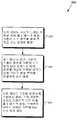
도 1은 본 발명의 일 실시예에 따른 예시적인 방법 단계들에 대응하는 흐름도이다.1 is a flowchart corresponding to exemplary method steps according to an embodiment of the present invention.
도 2A는 도 1의 흐름도의 특정 단계들에 대응하여, 본 발명의 상기 실시예에 따라 처리되는 웨이퍼의 일부분의 단면도이다.2A is a cross-sectional view of a portion of a wafer processed in accordance with the above embodiment of the present invention, corresponding to certain steps of the flowchart of FIG. 1.
도 2B는 도 1의 흐름도의 특정 단계들에 대응하여, 본 발명의 상기 실시예에 따라 처리되는 웨이퍼의 일부분의 단면도이다.2B is a cross-sectional view of a portion of the wafer being processed in accordance with the above embodiment of the present invention, corresponding to certain steps of the flowchart of FIG. 1.
도 2C는 도 1의 흐름도의 특정 단계들에 대응하여, 본 발명의 상기 실시예에 따라 처리되는 웨이퍼의 일부분의 단면도이다.2C is a cross-sectional view of a portion of a wafer being processed in accordance with the above embodiment of the present invention, corresponding to certain steps of the flowchart of FIG. 1.
도 2D는 도 1의 흐름도의 특정 단계들에 대응하여, 본 발명의 상기 실시예에 따라 처리되는 웨이퍼의 일부분의 단면도이다.2D is a cross-sectional view of a portion of a wafer being processed in accordance with the above embodiment of the present invention, corresponding to certain steps of the flowchart of FIG. 1.
도 3은 본 발명의 일 실시예에 따른 예시적인 방법 단계들에 대응하는 흐름도이다.3 is a flowchart corresponding to exemplary method steps in accordance with an embodiment of the present invention.
도 4A는 도 3의 흐름도의 특정 단계들에 대응하여, 본 발명의 상기 실시예에 따라 처리되는 웨이퍼의 일부분의 단면도이다.4A is a cross-sectional view of a portion of a wafer being processed in accordance with the above embodiment of the present invention, corresponding to certain steps of the flowchart of FIG. 3.
도 4B는 도 3의 흐름도의 특정 단계들에 대응하여, 본 발명의 상기 실시예에 따라 처리되는 웨이퍼의 일부분의 단면도이다.4B is a cross-sectional view of a portion of a wafer being processed in accordance with the above embodiment of the present invention, corresponding to certain steps of the flowchart of FIG. 3.
도 4C는 도 3의 흐름도의 특정 단계들에 대응하여, 본 발명의 상기 실시예에 따라 처리되는 웨이퍼의 일부분의 단면도이다.4C is a cross-sectional view of a portion of a wafer being processed in accordance with the above embodiment of the present invention, corresponding to certain steps of the flowchart of FIG. 3.
본 발명은 낮은 DIBL 및 Vss 저항을 갖는 메모리 셀에 관한 것이다. 이하의 상세한 설명은 본 발명의 실시에 적합한 특정 정보를 제시한다. 기술분야의 당업자는 본 발명이 본 출원에서 특정하게 논의된 것과는 다른 방식으로 구현될 수 있음을 인식할 것이다. 게다가, 본 발명의 구체적인 세부사항들 중 일부는 본 발명을 모호하게 하는 것을 방지하기 위해 논의되지 않는다.The present invention relates to a memory cell having a low DIBL and Vss resistance. The following detailed description presents specific information suitable for practicing the present invention. Those skilled in the art will recognize that the present invention may be implemented in a manner different from that specifically discussed in this application. In addition, some of the specific details of the invention are not discussed in order to avoid obscuring the invention.
본 출원의 도면들 및 이에 대응하는 상세한 설명은 단지 본 발명의 예시적인 실시예들에 관한 것이다. 간결성을 위해, 본 발명의 다른 실시예들은 본 출원에서 구체적으로 설명되지 않으며 첨부된 도면들에 의해 상세하게 도시되지 않는다.The drawings in the present application and their corresponding detailed description are directed to merely exemplary embodiments of the invention. For the sake of brevity, other embodiments of the invention are not described in detail in this application and are not shown in detail by the accompanying drawings.
도 1은 본 발명의 일 실시예에 따라 오목한 Vss 주입 영역과, 그리고 감소된 소스 흩어짐 및 확산을 갖는 소스를 구비한 부동 게이트 플래시 메모리 셀을 형성하는 예시적인 방법을 설명하는 흐름도이다. 본 기술 분야의 당업자에게 명백한 특정 세부사항들 및 피처(feature)들은 흐름도(100)에서 고려하지 않았다. 예를 들어, 기술분야에서 공지된 바와 같이, 하나의 단계는 하나 이상의 하위 단계들을 포함하거나 특수 장비 또는 재료들을 포함할 수 있다. 흐름도(100)에 기재된 단계들(170, 172, 174 및 176)은 본 발명의 일 실시예를 기술하기에 충분하며, 본 발명의 다른 실시예들은 흐름도(100)에 도시된 것과 다른 단계들을 이용할 수 있다. 흐름도(100)에 도시된 공정 단계들은, 단계(170) 이전에 기판상에 위치하는 부동 게이트 메모리 셀의 스택 게이트 구조를 포함하는 웨이퍼상에서 수행된다. 상기 스택 게이트는 기판상에 위치한 터널 옥사이드 층과, 상기 터널 옥사이드 층상에 위치한 부동 게이트와, 상기 부동 게이트상에 위치한 옥사이드-나이트라이드-옥사이드(ONO) 스택과, 그리고 상기 ONO 스택상에 위치한 제어 게이트를 또한 포함한다. 도 2A, 2B, 2C 및 2D의 구조들(270, 272, 274 및 276)은, 전술한 바와 같이 기판상에 위치한 스택 게이트 구조를 포함하는 구조상에, 흐름도(100)의 단계들(170, 172, 174 및 76)을 수행한 결과를 도시한다.1 is a flow diagram illustrating an exemplary method of forming a floating gate flash memory cell having a concave Vss implanted region and a source having reduced source scattering and diffusion in accordance with one embodiment of the present invention. Certain details and features that are apparent to those skilled in the art are not considered in the
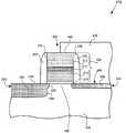
도1의 단계(170)와 도 2A의 구조(270)를 살펴보면, 흐름도(100)의 단계(170)에서는 저에너지 도핑 영역(218)이 소스 영역(222)에 형성되어 있고 저 에너지 도핑 영역(220)이 드레인 영역(224)에 형성되어 있다. 저 에너지 주입 도핑 영역들(218 및 220)은 소스 영역(222)과 드레인 영역(224)에 필요한 양의 적당한 N 타입 도펀트를 적절히 주입하도록 저 에너지/저 도오즈 주입(low energy/low dose implant)을 이용함으로써 형성될 수 있다. 저 에너지 주입 도핑 영역(218)은 측면 흩어짐 및 확산 에지(228)를 가지며, 상기 측면 흩어짐 및 확산 에지(228)는 스택 게이트 구조(208) 아래의 채널 영역(226)을 향해 연장된다. 일 실시예에서, 저 에너지 주입 도핑 영역(218)은 단계(170)에서 소스 영역(222)에 형성되고 저 에너지 주입 도핑 영역(220)은 상기 공정의 후속 단계에서 Vss 접속 영역을 형성한 후에 드레인 영역(224)에 형성된다. 구조(270)는 NOR 타입 플래시 메모리 디바이스와 같은 플래시 메모리 디바이스를 포함할 수 있다. 배경기술로서, NOR 타입 플래시 메모리 디바이스는, 소스 영역들이 전형적으로 워드라인들에 평행한 Vss 라인들에 의해 접속되는 NOR 구조로 구성된 플래시 메모리 디바이스이다. 부동 게이트 메모리 셀(202)은 NOR 타입 부동 게이트 플래시 메모리 셀과 같은 부동 게이트 플래시 메모리 셀일 수 있다. 저 에너지 주입 도핑 영역들(218 및 220)은 스택 게이트 구조(208) 아래의 기판(204)에 위치한 채널(226)로의 접속을 제공한다.Referring to
또한 도 2A에서 도시된 바와 같이, 스택 게이트 구조(208)는 기판(204) 상에 위치하고, 그리고 터널 옥사이드 층(210)과, 부동 게이트(212)와, ONO 스택(214)과, 그리고 제어 게이트(216)를 포함한다. 또한 도 2A에 도시된 바와 같이, 터널 옥사이드 층(210)은 기판(204)의 상부 표면(206) 상의 채널 영역(226) 위에 위치한다. 또한 도2A에 도시된 바와 같이, 부동 게이트(212)는 터널 옥사이드 층(210) 상에 위치하고, 그리고 폴리실리콘(polysilicon)이라고도 불리는 다결정 실리콘을 포함할 수 있으며, 이는 저압 화학 증기 증착(LPCVD: low pressure chemical vapor deposition) 또는 다른 적당한 공정들에 의해 증착될 수 있다. 또한 도 2A에 도시된 바와 같이, ONO 스택(214)은 부동 게이트(212) 상에 위치한다. ONO 스택(214)은 실리콘 옥사이드의 바닥층과, 실리콘 나이트라이드의 중간층과, 그리고 실리콘 옥사이드의 상부층으로 구성된 3층 구조이며, 이는 LPCVD 공정에 의해 순차적으로 증착되거나 또는 열적으로 성장될 수 있다. 또한 도 2A에 도시된 바와 같이, 제어 게이트(216)는 ONO 스택(214) 상에 위치하며 폴리실리콘으로 구성될 수 있고, 이는 LPCVD 공정 또는 다른 적당한 공정들에 의해 ONO 스택(214) 상에 형성될 수 있다. 또한 도 2A에 도시된 바와 같이, 소스 영역(222) 및 드레인 영역(224)은 스택 게이트 구조(208)에 인접하여 기판(204) 내에 위치하며 종래 기술에서 공지된 방식으로 형성될 수 있다. 도 2A에서, 흐름도(100)의 단계(170)의 결과물로서 구조(270)가 예시되어 있다.As also shown in FIG. 2A, the
도 1의 단계(172)와 도2B의 구조(272)를 계속에서 살펴보면, 흐름도(100)의 단계(172)에서, 스페이서들(230 및 232)이 스택 게이트 구조(208)의 소스 및 드레인 측벽들(234 및 236) 각각에 인접하여 형성되며, 마스크가 스택 게이트 구조(208)의 드레인 측 부분(242)의 위 및 드레인 영역(224)의 위에 형성되고, 그리고 고 에너지 주입 도핑 영역(240)이 기판(204)의 소스 영역(222)에 형성된다. 본 실시예에서, 스택 게이트 구조(208)의 소스 및 드레인 측벽들(234 및 236) 각각에 인접하여 위치하는 스페이서들(230 및 232)은 실리콘 옥사이드를 포함할 수 있다. 다른 실시예에서, 스페이서들(230 및 232)은 다른 적당한 유전체 물질(dielectric material)을 포함할 수 있다. 스페이서들(230 및 232)은 LPCVD 공정 또는 다른 적당한 공정들에 의해 스택 게이트 구조 위에 실리콘 옥사이드의 컨포멀층(conformal layer)을 증착함으로써 형성될 수 있다. 상기 증착된 실리콘 옥사이드의 컨포멀층은 적당한 에치(etch) 공정을 사용하여 "에치백(etch back)"되어 스페이서들(230 및 232)을 형성할 수 있다.Continuing with the
도 2B에 도시된 바와 같이, 마스크(238)는 기판(204)의 드레인 영역(224) 위 및 스택 게이트 구조(208)의 드레인측 부분(242) 위에 위치한다. 마스크(238)는 자기정렬 소스(SAS:self-aligned source) 마스크일 수 있으며, 이는 기술분야에 공지된 방식으로 형성될 수 있으며, 그리고 포토레지스트(photoresist)와 같은 적당한 마스크 물질을 포함할 수 있다. 도 2B에 도시된 바와 같이, 고 에너지 주입 도핑 영역(240)은 소스 영역(222)에 위치하며 저 에너지 주입 도핑 영역(218)으로 연장된다. 고 에너지 주입 도핑 영역(240)은 측면 흩어짐 및 확산 에지(244)를 가지며, 그리고 소스 영역(222)에 필요한 양의 적당한 N 타입 도펀트를 적절히 주입하도록 고 에너지/고 도오즈 주입을 사용하여 형성될 수 있다. 도 2B에서, 상기 흐름도(100)의 단계(172)의 결과물로서 구조(272)가 예시된다.As shown in FIG. 2B,
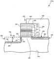
도 1의 단계(174) 및 도 2C의 구조(274)를 계속 살펴보면, 흐름도(100)의 단계(174)에서, 어닐링(anneal) 공정이 수행되고, 스페이서(230)가 제거되고, 그리고 오목부(246)가 기판(204)의 소스 영역(222)에 형성된다. 어닐링 공정 동안에, 고 에너지 주입 도핑 영역(240)을 형성하는데 이용된 고 에너지 주입으로 인해 야기된 손상이 복구될 수 있도록 기판(204)이 충분한 온도까지 가열된다. 상기 어닐링 공정은 고 에너지 주입 도핑 영역(240)을 형성하는데 사용되는 고 에너지 주입의 에너지가 감소되도록 하여, 스택 게이트 구조(208) 아래로의 고 에너지 주입 도핑 영역(240)의 측면 흩어짐 및 확산이 줄어든다. 상기 어닐링 공정은 저 에너지 주입 도핑 영역(218)과 고 에너지 주입 도핑 영역(240) 각각의 측면 흩어짐 및 확산 에지들(228 및 244)(도 2B에 도시됨)을 고르게(smooth out) 할 수 있다. 일 실시예에서, 상기 어닐링 공정은 이용되지 않는다. 이러한 실시예에서, 상기 고 에너지 주입의 에너지는, 상기 측면 흩어짐 및 확산 에지(244)(도 2B에 도시됨)가 기판(204)의 상부 표면(206)에 평행한 방향에서 측정할 때 스택 게이트 구조(208)의 소스 측벽(234)을 넘어 적당한 거리로 연장되는 것을 보장할 수 있도록, 적당히 증가될 수 있다.Continuing with
도 2C에 또한 도시된 바와 같이, 스페이서(234)는 제거되고, 그리고 오목부(246)가 소스 영역(222)에 형성된다. 스페이서(234)는 SAS 에치 공정을 이용하여 제거될 수 있으며, 상기 SAS 에치 공정은 기판(204)에서 저 에너지 주입 도핑 영역(218)과 고 에너지 주입 도핑 영역(240)의 상당 부분을 에치함으로써 오목부(246)를 형성하도록 이용될 수 있다. 오목부(246)는 측벽(248)과, 바닥(250)과, 그리고 깊이(252)를 가지며, 상기 깊이(252)는 오목부(246)의 바닥(250)과 기판(204)의 상부 표면(206) 사이의 거리를 표시한다. 예시로서, 깊이(252)는 대략 100.0Å 내지 대략 500.0Å일 수 있다. 본 실시예에서, 오목부(246)의 측벽(248)은 기판(204)의 상부 표면(206)에 실질적으로 수직일 수 있다. 다른 실시예에서, 오목부(2460의 측벽(248)은 기판(204)의 상부 표면(206)에 대해 대략 90.0℃ 이외의 각도를 형성할 수 있다. SAS 에치 공정 동안에, 옥사이드가 얕은 트렌치 절연(STI:shallow trench isolation) 영역들(도면에 도시되지 않음)로부터 또한 제거 되어 후속 Vss 접속 주입에 대비하여 트렌치들을 노출시킬 수 있다.As also shown in FIG. 2C, the
도 2C에 도시된 바와 같이, 고 에너지 주입 도핑 영역(240) 및 저 에너지 주입 도핑 영역(218)(도2B에 도시됨)의 상당 부분이 제거된 후에, 고 에너지 주입 도핑 영역(240)과 저 에너지 주입 도핑 영역(218)의 나머지 부분들이 부동 게이트 메모리 셀(202)의 소스(254)를 형성한다. 도 2C에 도시된 바와 같이, 소스 접합(256)을 갖는 소스(254)는 오목부(246)의 측벽(248)에 인접하여 위치하고 그리고 또한 스택 게이트 구조(208)의 아래에 위치한다. 또한 도2C에 도시된 바와 같이, 고 에너지 주입 도핑 영역(240)의 부분(258)은 오목부(246)의 형성 후에도 잔존하며 오목부(246)의 바닥 아래에 위치한다. 고 에너지 주입 도핑 영역(240)의 부분(258)은 소스(254)에 접속되어, 후속 공정 단계에서 형성되는 Vss 접속 영역과 소스(254) 사이에 충분한 접속을 보장한다. 도2C에서, 흐름도(100)의 단계(174)의 결과물이 구조(274)로서 예시된다.As shown in FIG. 2C, after a significant portion of the high energy implantation doped
이제 도 1의 단계(176)와 도 2D를 살펴보면, 흐름도(100)의 단계(176)에서, 마스크(238)(도 2C에 도시됨)가 제거되고, 마스크(260)가 드레인 영역(224) 위 및 스택 게이트 구조(208)의 드레인측 부분(242) 위에 형성되고, 그리고 Vss 접속 영역(262)이 오목부(246)의 바닥(250) 아래의 기판(204)에 형성된다. 마스크(238)가 기술분야의 공지된 방식으로 제거될 수 있다. 도2D에 도시된 바와 같이, 마스크(260)는 드레인 영역(224) 위 및 스택 게이트 구조(208)의 드레인측 부분(242) 위에 위치할 수 있으며, SAS 마스크일 수 있다. 마스크(260)는 마스크(238)의 조성 및 형상과 실질적으로 유사하다.Referring now to step 176 and FIG. 2D of FIG. 1, in
또한 도2D에 도시된 바와 같이, Vss 접속 영역(262)이 오목부(254)의 바닥(250) 아래 및 부동 게이트 메모리 셀(202)의 소스(254)에 위치한다. Vss 접속 영역(262)은 고 에너지 주입 도핑 영역(240)(도2B에 도시됨)의 부분(258) 내로 연장되며, 이 부분(258)은 Vss 접속 영역(262)을 부동 게이트 메모리 셀(202)의 소스(254)에 접속된다. Vss 접속 영역(262)은 강하게 도핑된 영역(heavily doped region)이며, Vss 접속 주입에 의해 형성될 수 있으며, 상기 Vss 접속 주입은 적당한 N 타입 도펀트를 포함하는 고 에너지/고 도오즈 주입이다. Vss 접속 영역(262)은 공통 소스 라인을 형성하고, 이는 다른 부동 게이트 메모리 셀들(도면들에 도시되지 않음)의 소스 영역들을 공통 그라운드(common ground)로 접속하는데 이용된다. Vss 접속 영역(262)은 본 출원에서 "Vss 저항"이라고도 지칭되는 저항을 갖는다.Also shown in FIG. 2D, a
도1의 본 발명의 실시예에서, 스페이서(230)는 고 에너지 주입 도핑 영역(240)의 측면 흩어짐 및 확산을 줄이고, 이에 따라 채널 영역(226)으로의 소스(254)의 측면 흩어짐 및 확산을 줄이는데 사용될 수 있으며, 이는 바람직하지 않게 채널 영역(226)의 유효 채널 길이가 축소되는 것을 방지한다. 또한, 도1의 본 발명의 실시예에서, 오목부(246)는 Vss 접속 영역(262)이 소스(254) 아래에 위치하도록 하는데 이용되며, 이는 채널 영역(226)으로의 소스(254)의 측면 흩어짐 및 확산을 줄인다. 따라서, 채널 영역(226)으로의 소스(254)의 측면 흩어짐 및 확산을 줄임으로써, 도1의 본 발명의 실시예는 부동 게이트 메모리 셀(202)에서 DIBL을 유리하게 감소시킬 수 있다. 또한, 채널 영역(226)으로의 고 에너지 주입 도핑 영역(240)의 측면 흩어짐 및 확산을 줄이는데 스페이서(230)를 사용함으로써, 고 에 너지 주입 도핑 영역(240)을 형성하는데 사용되는 고 에너지 주입이 소스(254)와 Vss 접속 영역(262) 사이에 적절한 접속을 보장하는 충분한 에너지 및 도오즈를 가질 수 있도록 하면서, Vss 접속 영역(262)이 기판(204)의 상부 표면(206) 아래로 적당한 거리에 위치될 수 있도록 한다.In the embodiment of the present invention of FIG. 1, the
추가적으로, 도1의 본 발명의 실시예에서, Vss 접속 영역(262)이 기판(204)의 상부 표면(206) 아래 및 소스(254) 아래에 위치하도록 오목부(246)를 사용함으로써, Vss 접속 영역(238)의 저항, 즉 Vss 저항은, DIBL을 바람직하지 않게 증가시킴이 없이 Vss 접속 영역(262)을 강하게 도핑함으로써 감소될 수 있다.Additionally, in the embodiment of the present invention of FIG. 1, by using the
도 3은 본 발명의 일 실시예에 따라 축소된 소스 확산을 갖는 소스와 오목한 Vss 주입 영역을 포함하는 부동 게이트 플래시 메모리 셀을 형성하는 예시적인 방법을 설명하는 흐름도를 도시한다. 기술분야의 당업자에게 명백한 특정 세부사항들 및 피처(feature)들은 흐름도(300)에서 고려하지 않았다. 예를 들어, 기술분야에서 공지된 바와 같이, 하나의 단계는 하나 이상의 하위 단계들을 포함하거나 특수 장비 또는 재료들을 포함할 수 있다. 흐름도(300)에 기재된 단계들(370, 372 및 374)은 본 발명의 일 실시예를 기술하기에 충분하며, 본 발명의 다른 실시예들은 흐름도(300)에 도시된 것과 다른 단계들을 이용할 수 있다. 흐름도(300)에 도시된 공정 단계들은, 단계(370) 이전에 스택 게이트 구조에 인접하여 위치하는 소스 및 드레인 영역들을 갖는 기판상에 위치하는 부동 게이트 메모리 셀의 스택 게이트 구조를 포함하는 웨이퍼 상에서 수행된다. 상기 스택 게이트는 기판상에 위치한 터널 옥사이드 층과, 상기 터널 옥사이드 층상에 위치한 부동 게이트와, 상기 부동 게이트상에 위치한 ONO 스택과, 그리고 상기 ONO 스택상에 위치한 제어 게이트를 또한 포함한다. 도 4A, 4B, 및 4C의 구조들(470, 472 및 474)은, 전술한 바와 같이 기판상에 위치한 스택 게이트 구조를 포함하는 구조상에, 흐름도(300)의 단계들(370, 372 및 374)을 각각 수행한 결과를 도시한다.3 depicts a flow diagram illustrating an exemplary method of forming a floating gate flash memory cell comprising a source with reduced source diffusion and a concave Vss implanted region in accordance with one embodiment of the present invention. Certain details and features that are apparent to those skilled in the art are not considered in the
도 3의 단계(370)과 도4A의 구조(470)를 살펴보면, 흐름도(300)의 단계(370)에서 마스크(438)가 스택 게이트 구조(408)의 드레인측 부분(442)의 위 및 기판(404)의 드레인 영역(424) 위에 형성되고, 그리고 오목부(464)가 기판(404)의 소스 영역(422)에 형성된다. 도4A에서, 구조(470) 내의 부동 게이트 메모리 셀(402)과, 기판(404)과, 상부 표면(406)과, 스택 게이트 구조(408)와, 터널 옥사이드 층(410)과, 부동 게이트(412)와, ONO 스택(414)과, 제어 게이트(416)와, 소스 영역(422)과, 드레인 영역(424)과, 그리고 채널 영역(426)은 각각, 도2A의 구조(270)의 부동 게이트 메모리 셀(202)과, 기판(204)과, 상부 표면(206)과, 스택 게이트 구조(208)와, 터널 옥사이드 층(210)과, 부동 게이트(212)와, ONO 스택(214)과, 제어 게이트(216)와, 소스 영역(222)과, 드레인 영역(224)과, 그리고 채널 영역(226)에 대응한다.Referring to step 370 of FIG. 3 and the
도4A에 도시된 바와 같이, 마스크(438)는 스택 게이트 구조(408)의 드레인측 부분(442) 위 및 기판(404)의 드레인 영역(424) 위에 위치한다. 마스크(438)는 도2B의 마스크(238)와 그 형상 및 조성이 실질적으로 유사하다. 도2A의 구조(270)와 유사하게, 구조(470)는 NOR 타입 플래시 메모리 디바이스와 같은 플래시 메모리 디바이스를 포함할 수 있다. 도 4A에 도시된 바와 같이, 오목부(464)는 소스 영 역(422)에 위치하고, 그리고 경사 측벽(sloped sidewall) (466)과, 바닥(468)과, 그리고 깊이(476)을 가지며, 여기서 상기 깊이(476)는 기판(404)의 상부 표면(406)과 바닥(468) 사이의 거리를 나타낸다. 예시로서, 깊이(476)는 대략 100.0Å 내지 대략 500.0Å일 수 있다. 경사 측벽(466)은 기판(404)의 상부 표면(406)에 대해서 각도(478)를 형성한다. 예시로서, 상기 각도(478)는 대략 85.0°내지 대략 89.0°일 수 있다. 오목부(464)는 소스 영역(422)에서 기판(404)의 일부분을 에치하도록 SAS 에치 공정을 이용함으로써 형성될 수 있다. SAS 에치 공정 동안에, 옥사이드가 얕은 트렌치 절연(STI) 영역들(도면들에 도시되지 않음)로부터 또한 제거되어 후속 Vss 접속 주입을 대비하여 트렌치들을 노출시킨다.As shown in FIG. 4A, a
또한 도4A에 도시된 바와 같이, 스택 게이트 구조(408)가 기판(404) 상에 위치하며, 그리고 터널 옥사이드 층(410)과, 부동 게이트(412)와, ONO 스택(414)과, 그리고 제어 게이트(416)를 포함한다. 또한 도4A에 도시된 바와 같이, 터널 옥사이드 층(410)이 기판(404)의 상부 표면(406) 상의 채널 영역(426) 위에 위치하고, 부동 게이트(412)가 터널 옥사이드 층(410) 상에 위치하며, ONO 스택(414)이 부동 게이트(412) 상에 위치하며, 그리고 제어 게이트(216)가 ONO 스택(414) 상에 위치한다. 또한 도4A에 도시된 바와 같이, 소스 영역(422) 및 드레인 영역(424)은 각각 스택 게이트 구조(408)의 소스 측벽(480)과 드레인 측벽(482)에 인접하여 기판(404)에 위치한다. 도4A에서, 흐름도(300)의 단계(370)의 결과물이 구조(470)로 예시된다.As also shown in FIG. 4A, a
도3의 단계(372)와 도4B의 구조(472)를 계속 살펴보면, 흐름도(300)의 단계(372)에서, 마스크(438)가 제거되고, 가볍게(lightly) 도핑된 영역들(484 및 486)이 각각 소스 영역(422)과 드레인 영역(424)에 형성되고, 그리고 소스(488)가 오목부(464)의 경사 측벽(466)에 인접하여 형성된다. 마스크(438)는 기술분야에서 공지된 적당한 에치 공정을 이용함으로써 제거될 수 있다. 도4B에 도시된 바와 같이, 가볍게 도핑된 영역(484)은 오목부(464)의 바닥(468) 아래에 위치하고 그리고 가볍게 도핑된 영역(486)은 드레인 영역(424)에 위치한다. 일 실시예에서, 가볍게 도핑된 영역(484)이 흐름도(300)의 단계(372)에서 소스 영역(422)에 형성되고 그리고 공정의 후속 단계에서 Vss 접속 영역을 형성한 후에 가볍게 도핑된 영역(486)이 드레인 영역(424)에 형성된다. 또한 도4B에 도시된 바와 같이, 소스(488)는 오목부(464)의 경사 측벽(466)에 인접하게 위치하고, 가볍게 도핑된 영역을 포함한다. 가볍게 도핑된 영역들(484 및 486) 및 소스(488)는 소스 영역(422) 및 드레인 영역(424)에 필요한 양의 적당한 N 타입 도펀트를 적절히 주입하도록 저 에너지/저 도오즈 주입을 이용함으로써 형성될 수 있다. 도4B에서, 흐름도(300)의 단계(372)의 결과물이 구조(472)로서 예시된다.Continuing with
도3의 단계(374) 및 도4C의 구조(474)를 계속 살펴보면, 흐름도(300)의 단계(374)에서, 스페이서들(490 및 492)이 스택 게이트 구조(408)에 인접하여 형성되고, 마스크(494)가 드레인 영역(424)과 스택 게이트 구조(408)의 드레인측 부분(442) 위에 형성되고, 그리고 Vss 접속 영역(496)이 오목부(464)의 바닥(468) 아래의 기판(404)에 형성된다. 도4C에 도시된 바와 같이, 마스크(494)가 스택 게이트 구조(408)의 드레인측 부분(442) 위에 위치하며, 또한 마스크(438)의 조성 및 형상과 실질적으로 유사하다. 또한 도4C에 도시된 바와 같이, 스페이서(490)가 스택 게이트 구조(408)의 소스 측벽(480)에 인접하여 그리고 오목부(464)의 경사 측벽(466)에 인접하여 위치하며, 그리고 스페이서(492)는 스택 게이트 구조(408)의 드레인 측벽(482)에 인접하여 위치한다. 스페이서(490)는 오목부(464)의 바닥(468)까지 연장된다. 스페이서들(490 및 492)은 실리콘 옥사이드를 포함할 수 있고, 그리고 LPCVD 또는 다른 적당한 공정들을 사용하여 스택 게이트 구조(408) 위에 실리콘 옥사이드의 컨포멀층을 증착함으로써 형성될 수 있다. 상기 증착된 실리콘 옥사이드의 컨포멀층은 스페이서들(490 및 492)을 형성하도록 적당한 에치 공정을 통해 "에치백"될 수 있다.Continuing with the
도4C에 또한 도시된 바와 같이, Vss 접속 영역(496)은 오목부(464)의 바닥(468) 아래 및 소스(488) 아래에 위치한다. Vss 접속 영역(496)은 가볍게 도핑된 영역(484) 내로 연장되며, 이 영역(484)은 Vss 접속 영역(494)을 부동 게이트 메모리 셀(402)의 소스(488)로 접속한다. Vss 접속 영역(496)은 도 2D의 Vss 접속 영역(262)의 형상 및 조성과 실질적으로 유사하다. 도2D의 Vss 접속 영역(262)과 유사하게, Vss 접속 영역(496)은 공통 소스 라인을 형성하며, 여기서 상기 공통 소스 라인은 다른 부동 게이트 메모리 셀들(도면들에 도시되지 않음)의 소스 영역들을 공통 그라운드로 접속하는데 이용된다. Vss 접속 영역(496)은 도2D의 Vss 접속 영역(262)과 실질적으로 유사한 저항을 갖는다. 도4C에서, 흐름도(300)의 단계(374)의 결과물이 구조(474)로 예시된다.As also shown in FIG. 4C, the
도3의 본 발명의 실시예에서, 경사 측벽(466)을 갖는 오목부(464)를 형성함으로써, 저 에너지/저 도오즈 주입이 경사 측벽(466)에 인접하게 위치하는 소스(488)와 소스(488)로 접속되는 가볍게 도핑된 영역(484)을 형성하는데 이용될 수 있다. 또한, Vss 접속 영역(496)을 형성하는데 이용되는 고 에너지/고 도오즈 주입으로부터 소스(488)를 보호하는데 스페이서(490)를 이용하고 그리고 소스(488) 아래에 Vss 접속 영역(496)을 형성하는데 오목부(464)를 이용함으로써, 도3의 본 발명의 실시예는 채널 영역(426)으로의 소스(488)의 측벽 흩어짐 및 확산을 유리하게 줄일 수 있다. 채널 영역(426)으로의 소스(488)의 측면 흩어짐 및 확산을 줄임으로써, 도3의 본 발명의 실시예는 부동 게이트 메모리 셀(402)에서 유리하게 DIBL을 줄일 수 있다. 추가적으로, 도3의 본 발명의 실시예에서, 소스(488)의 아래 및 기판(404)의 상부 표면(406) 아래에 Vss 접속 영역(496)을 위치시키는데 오목부(464)를 이용하고 그리고 소스(488)를 보호하는데 스페이서(490)를 이용함으로써, 바람직하지 않게 DIBL을 증가시킴이 없이, Vss 접속 영역(496)을 강하게 도핑하여 Vss 접속 영역(96)의 저항, 즉 Vss 저항이 감소될 수 있다.In the embodiment of FIG. 3, by forming a
전술한 바와 같이, 도1 및 도3의 본 발명의 실시예들은 스페이서 및 오목한 Vss 접속 영역을 가짐으로써 NOR 타입 부동 게이트 플래시 메모리 셀과 같은 부동 게이트 메모리 셀에서 DIBL 및 Vss 저항을 낮출 수 있다.As described above, the embodiments of the present invention of FIGS. 1 and 3 can lower DIBL and Vss resistance in floating gate memory cells such as NOR type floating gate flash memory cells by having spacers and concave Vss connection regions.
본 발명의 상기 예시적인 실시예들로부터, 다양한 기술들이 본 발명의 범위를 벗어남이 없이 본 발명의 사상을 구현하는데 사용될 수 있음이 명백하다. 더욱이, 본 발명이 특정 실시예들을 참조하여 설명되었지만, 기술분야의 당업자라면 본 발명의 사상 및 범위를 벗어남이 없이 형상 및 세부사항들에 수정 및 변경이 가해 질 수 있음을 인식할 것이다. 상술한 예시적인 실시예들은 단지 예시적인 것으로 간주되어야 하며 제한적으로 해석되어서는 아니된다. 또한 본 발명이 본 출원에 개시된 특정 예시적인 실시에들로 제한되지 않고, 본 발명의 범위를 벗어남이 없이 수많은 수정, 변경, 및 치환이 가능함을 이해해야 한다.From the above exemplary embodiments of the present invention, it is apparent that various techniques may be used to implement the spirit of the present invention without departing from the scope of the present invention. Moreover, while the invention has been described with reference to specific embodiments, those skilled in the art will recognize that modifications and changes may be made in shape and details without departing from the spirit and scope of the invention. The illustrative embodiments described above are to be regarded as illustrative only and should not be construed as limiting. It is also to be understood that the invention is not limited to the specific exemplary embodiments disclosed in this application, and that numerous modifications, changes, and substitutions may be made without departing from the scope of the invention.
본 발명에 따르면 DIBL 및 Vss 저항이 감소된 메모리 셀이 획득될 수 있다.According to the present invention, memory cells having reduced DIBL and Vss resistances can be obtained.
Claims (10)
Translated fromKoreanApplications Claiming Priority (2)
| Application Number | Priority Date | Filing Date | Title |
|---|---|---|---|
| US10/915,771 | 2004-08-11 | ||
| US10/915,771US7170130B2 (en) | 2004-08-11 | 2004-08-11 | Memory cell with reduced DIBL and Vss resistance |
Publications (2)
| Publication Number | Publication Date |
|---|---|
| KR20070041782A KR20070041782A (en) | 2007-04-19 |
| KR100838387B1true KR100838387B1 (en) | 2008-06-13 |
Family
ID=34967972
Family Applications (1)
| Application Number | Title | Priority Date | Filing Date |
|---|---|---|---|
| KR1020077005665AExpired - Fee RelatedKR100838387B1 (en) | 2004-08-11 | 2005-04-29 | Floating gate memory cell |
Country Status (7)
| Country | Link |
|---|---|
| US (1) | US7170130B2 (en) |
| EP (1) | EP1782460B1 (en) |
| JP (2) | JP4642077B2 (en) |
| KR (1) | KR100838387B1 (en) |
| CN (1) | CN1993817B (en) |
| TW (1) | TWI382473B (en) |
| WO (1) | WO2006022907A1 (en) |
Families Citing this family (6)
| Publication number | Priority date | Publication date | Assignee | Title |
|---|---|---|---|---|
| US7151028B1 (en)* | 2004-11-04 | 2006-12-19 | Spansion Llc | Memory cell with plasma-grown oxide spacer for reduced DIBL and Vss resistance and increased reliability |
| US7732877B2 (en)* | 2007-04-02 | 2010-06-08 | Taiwan Semiconductor Manufacturing Company, Ltd. | Gated diode with non-planar source region |
| US9412598B2 (en) | 2010-12-20 | 2016-08-09 | Cypress Semiconductor Corporation | Edge rounded field effect transistors and methods of manufacturing |
| US8263458B2 (en) | 2010-12-20 | 2012-09-11 | Spansion Llc | Process margin engineering in charge trapping field effect transistors |
| US8999794B2 (en)* | 2011-07-14 | 2015-04-07 | Taiwan Semiconductor Manufacturing Company, Ltd. | Self-aligned source and drain structures and method of manufacturing same |
| JP7595411B2 (en) | 2019-11-22 | 2024-12-06 | デクセリアルズ株式会社 | Reel parts, adhesive film rolls |
Citations (2)
| Publication number | Priority date | Publication date | Assignee | Title |
|---|---|---|---|---|
| US5502321A (en)* | 1993-11-08 | 1996-03-26 | Sharp Kabushiki Kaisha | Flash memory having inclined channel |
| KR20020070859A (en)* | 2001-03-01 | 2002-09-11 | 주식회사 하이닉스반도체 | Transistor and memory cell with ultra-short gate feature and method of fabricating the same |
Family Cites Families (22)
| Publication number | Priority date | Publication date | Assignee | Title |
|---|---|---|---|---|
| IT1213218B (en) | 1984-09-25 | 1989-12-14 | Ates Componenti Elettron | PROCESS FOR THE MANUFACTURE OF A NON-VOLATILE MEMORY CELL WITH A VERY SMALL SIZE OF THIN OXIDE, AND A CELL OBTAINED BY THE ABOVE PROCESS. |
| JPH0812885B2 (en)* | 1987-03-03 | 1996-02-07 | 日本電気株式会社 | Nonvolatile semiconductor memory device |
| JP2957283B2 (en)* | 1990-12-06 | 1999-10-04 | 株式会社東芝 | Nonvolatile semiconductor memory device, method of manufacturing the same, and semiconductor device |
| JP3065164B2 (en)* | 1992-03-18 | 2000-07-12 | 富士通株式会社 | Semiconductor device and manufacturing method thereof |
| US5424233A (en)* | 1994-05-06 | 1995-06-13 | United Microflectronics Corporation | Method of making electrically programmable and erasable memory device with a depression |
| US6362504B1 (en) | 1995-11-22 | 2002-03-26 | Philips Electronics North America Corporation | Contoured nonvolatile memory cell |
| JP3548834B2 (en)* | 1996-09-04 | 2004-07-28 | 沖電気工業株式会社 | Manufacturing method of nonvolatile semiconductor memory |
| US5990509A (en)* | 1997-01-22 | 1999-11-23 | International Business Machines Corporation | 2F-square memory cell for gigabit memory applications |
| JPH10223868A (en)* | 1997-02-12 | 1998-08-21 | Mitsubishi Electric Corp | Nonvolatile semiconductor memory device and method of manufacturing the same |
| JP2964993B2 (en)* | 1997-05-28 | 1999-10-18 | 日本電気株式会社 | Semiconductor storage device |
| JPH1167937A (en) | 1997-08-12 | 1999-03-09 | Sony Corp | Semiconductor non-volatile storage device and manufacture thereof |
| JP3296415B2 (en)* | 1997-09-03 | 2002-07-02 | 日本電気株式会社 | Manufacturing method of nonvolatile semiconductor memory device |
| JPH11145430A (en)* | 1997-11-10 | 1999-05-28 | Nec Corp | Manufacture of semiconductor device |
| JPH11307744A (en)* | 1998-04-17 | 1999-11-05 | Ricoh Co Ltd | Semiconductor device and manufacturing method thereof |
| JP3246447B2 (en)* | 1998-07-21 | 2002-01-15 | 日本電気株式会社 | Method of manufacturing nonvolatile semiconductor memory device |
| KR100356471B1 (en)* | 1999-12-29 | 2002-10-18 | 주식회사 하이닉스반도체 | Method of manufacturing a flash EEPROM cell |
| KR100381953B1 (en)* | 2001-03-16 | 2003-04-26 | 삼성전자주식회사 | Method of fabricating nor type flash memory device |
| JP2003037193A (en)* | 2001-07-25 | 2003-02-07 | Mitsubishi Electric Corp | Nonvolatile semiconductor memory device and method of manufacturing the same |
| US6753242B2 (en)* | 2002-03-19 | 2004-06-22 | Motorola, Inc. | Integrated circuit device and method therefor |
| JP2004055826A (en)* | 2002-07-19 | 2004-02-19 | Renesas Technology Corp | Method for manufacturing semiconductor device |
| JP2004235399A (en)* | 2003-01-30 | 2004-08-19 | Renesas Technology Corp | Nonvolatile semiconductor memory device |
| JP2006135011A (en)* | 2004-11-04 | 2006-05-25 | Renesas Technology Corp | Semiconductor storage device |
- 2004
- 2004-08-11USUS10/915,771patent/US7170130B2/ennot_activeExpired - Lifetime
- 2005
- 2005-04-29JPJP2007525601Apatent/JP4642077B2/ennot_activeExpired - Fee Related
- 2005-04-29EPEP05742968Apatent/EP1782460B1/ennot_activeCeased
- 2005-04-29CNCN2005800264475Apatent/CN1993817B/ennot_activeExpired - Fee Related
- 2005-04-29WOPCT/US2005/014978patent/WO2006022907A1/enactiveApplication Filing
- 2005-04-29KRKR1020077005665Apatent/KR100838387B1/ennot_activeExpired - Fee Related
- 2005-08-02TWTW094126153Apatent/TWI382473B/ennot_activeIP Right Cessation
- 2010
- 2010-10-07JPJP2010227080Apatent/JP5452441B2/ennot_activeExpired - Fee Related
Patent Citations (2)
| Publication number | Priority date | Publication date | Assignee | Title |
|---|---|---|---|---|
| US5502321A (en)* | 1993-11-08 | 1996-03-26 | Sharp Kabushiki Kaisha | Flash memory having inclined channel |
| KR20020070859A (en)* | 2001-03-01 | 2002-09-11 | 주식회사 하이닉스반도체 | Transistor and memory cell with ultra-short gate feature and method of fabricating the same |
Also Published As
| Publication number | Publication date |
|---|---|
| WO2006022907A1 (en) | 2006-03-02 |
| KR20070041782A (en) | 2007-04-19 |
| JP2008509571A (en) | 2008-03-27 |
| EP1782460A1 (en) | 2007-05-09 |
| US20060035431A1 (en) | 2006-02-16 |
| CN1993817A (en) | 2007-07-04 |
| CN1993817B (en) | 2011-11-02 |
| EP1782460B1 (en) | 2011-06-01 |
| JP2011049576A (en) | 2011-03-10 |
| JP5452441B2 (en) | 2014-03-26 |
| US7170130B2 (en) | 2007-01-30 |
| TWI382473B (en) | 2013-01-11 |
| TW200620482A (en) | 2006-06-16 |
| JP4642077B2 (en) | 2011-03-02 |
Similar Documents
| Publication | Publication Date | Title |
|---|---|---|
| KR100586647B1 (en) | Flash memory device and manufacturing method thereof | |
| US6180980B1 (en) | Trench non-volatile memory cell | |
| JP5452441B2 (en) | Method for manufacturing a floating gate memory cell and floating gate memory cell | |
| KR100564434B1 (en) | Recess gate and manufacturing method thereof | |
| JP3360064B2 (en) | Method for manufacturing semiconductor device | |
| US20050158953A1 (en) | Method for fabricating an NROM memory cell arrangement | |
| KR100791331B1 (en) | Nonvolatile Memory Device and Manufacturing Method Thereof | |
| KR101092010B1 (en) | Structure and Method for Low Vs Resistance and Reduced DI in Floating Gate Memory Cells | |
| CN116419562B (en) | Semiconductor device and method for manufacturing the same | |
| US7151028B1 (en) | Memory cell with plasma-grown oxide spacer for reduced DIBL and Vss resistance and increased reliability | |
| KR100549010B1 (en) | Method of forming a transistor having a channel region on one sidewall of the channel portion hole | |
| KR20040036452A (en) | MOS Transistor and Method of manufacturing the same | |
| CN101355036B (en) | Trench gate semiconductor device and method for fabricating the same | |
| KR100341182B1 (en) | Method of forming mos transistor in semiconductor device | |
| JP5258193B2 (en) | Manufacturing method of floating gate type memory array | |
| CN116435188B (en) | High voltage device forming method and embedded flash memory device forming method | |
| JPH07106557A (en) | Semiconductor device and manufacture of the same | |
| KR100943133B1 (en) | Transistors in semiconductor devices and methods of forming them | |
| CN113948395A (en) | FinFET threshold voltage adjustment method | |
| JP3920383B2 (en) | Method for manufacturing double-thick floating gate oxide flash memory cell | |
| KR100589741B1 (en) | How to fabricate NVRM memory cell components | |
| CN113764349A (en) | Manufacturing method of semiconductor device | |
| KR20000003620A (en) | Fabricating method of semiconductor device | |
| JP2008112784A (en) | Semiconductor memory device and manufacturing method thereof | |
| KR20100033031A (en) | Manufacturing method of semiconductor device |
Legal Events
| Date | Code | Title | Description |
|---|---|---|---|
| E13-X000 | Pre-grant limitation requested | St.27 status event code:A-2-3-E10-E13-lim-X000 | |
| PA0105 | International application | St.27 status event code:A-0-1-A10-A15-nap-PA0105 | |
| A201 | Request for examination | ||
| PA0201 | Request for examination | St.27 status event code:A-1-2-D10-D11-exm-PA0201 | |
| PG1501 | Laying open of application | St.27 status event code:A-1-1-Q10-Q12-nap-PG1501 | |
| E902 | Notification of reason for refusal | ||
| PE0902 | Notice of grounds for rejection | St.27 status event code:A-1-2-D10-D21-exm-PE0902 | |
| E13-X000 | Pre-grant limitation requested | St.27 status event code:A-2-3-E10-E13-lim-X000 | |
| P11-X000 | Amendment of application requested | St.27 status event code:A-2-2-P10-P11-nap-X000 | |
| P13-X000 | Application amended | St.27 status event code:A-2-2-P10-P13-nap-X000 | |
| E701 | Decision to grant or registration of patent right | ||
| PE0701 | Decision of registration | St.27 status event code:A-1-2-D10-D22-exm-PE0701 | |
| GRNT | Written decision to grant | ||
| PR0701 | Registration of establishment | St.27 status event code:A-2-4-F10-F11-exm-PR0701 | |
| PR1002 | Payment of registration fee | St.27 status event code:A-2-2-U10-U12-oth-PR1002 Fee payment year number:1 | |
| PG1601 | Publication of registration | St.27 status event code:A-4-4-Q10-Q13-nap-PG1601 | |
| PR1001 | Payment of annual fee | St.27 status event code:A-4-4-U10-U11-oth-PR1001 Fee payment year number:4 | |
| PR1001 | Payment of annual fee | St.27 status event code:A-4-4-U10-U11-oth-PR1001 Fee payment year number:5 | |
| FPAY | Annual fee payment | Payment date:20130531 Year of fee payment:6 | |
| PR1001 | Payment of annual fee | St.27 status event code:A-4-4-U10-U11-oth-PR1001 Fee payment year number:6 | |
| FPAY | Annual fee payment | Payment date:20140527 Year of fee payment:7 | |
| PR1001 | Payment of annual fee | St.27 status event code:A-4-4-U10-U11-oth-PR1001 Fee payment year number:7 | |
| R18-X000 | Changes to party contact information recorded | St.27 status event code:A-5-5-R10-R18-oth-X000 | |
| LAPS | Lapse due to unpaid annual fee | ||
| PC1903 | Unpaid annual fee | St.27 status event code:A-4-4-U10-U13-oth-PC1903 Not in force date:20150610 Payment event data comment text:Termination Category : DEFAULT_OF_REGISTRATION_FEE | |
| R18-X000 | Changes to party contact information recorded | St.27 status event code:A-5-5-R10-R18-oth-X000 | |
| PC1903 | Unpaid annual fee | St.27 status event code:N-4-6-H10-H13-oth-PC1903 Ip right cessation event data comment text:Termination Category : DEFAULT_OF_REGISTRATION_FEE Not in force date:20150610 | |
| P22-X000 | Classification modified | St.27 status event code:A-4-4-P10-P22-nap-X000 |