KR100838082B1 - OLED display device and manufacturing method - Google Patents
OLED display device and manufacturing methodDownload PDFInfo
- Publication number
- KR100838082B1 KR100838082B1KR1020070026187AKR20070026187AKR100838082B1KR 100838082 B1KR100838082 B1KR 100838082B1KR 1020070026187 AKR1020070026187 AKR 1020070026187AKR 20070026187 AKR20070026187 AKR 20070026187AKR 100838082 B1KR100838082 B1KR 100838082B1
- Authority
- KR
- South Korea
- Prior art keywords
- pad
- pixel
- layer
- area
- insulating layer
- Prior art date
- Legal status (The legal status is an assumption and is not a legal conclusion. Google has not performed a legal analysis and makes no representation as to the accuracy of the status listed.)
- Active
Links
- 238000004519manufacturing processMethods0.000titleabstractdescription6
- 239000010410layerSubstances0.000claimsabstractdescription189
- 239000010408filmSubstances0.000claimsabstractdescription76
- 239000000758substrateSubstances0.000claimsabstractdescription48
- 238000002955isolationMethods0.000claimsabstractdescription37
- 238000000034methodMethods0.000claimsabstractdescription34
- 239000010409thin filmSubstances0.000claimsabstractdescription26
- 238000000926separation methodMethods0.000claimsabstractdescription17
- 239000003566sealing materialSubstances0.000claimsabstractdescription14
- 238000007789sealingMethods0.000claimsabstractdescription12
- 239000012044organic layerSubstances0.000claimsabstractdescription10
- 239000000463materialSubstances0.000claimsabstractdescription9
- 238000005538encapsulationMethods0.000claimsabstractdescription5
- 229910052581Si3N4Inorganic materials0.000claimsdescription9
- HQVNEWCFYHHQES-UHFFFAOYSA-Nsilicon nitrideChemical compoundN12[Si]34N5[Si]62N3[Si]51N64HQVNEWCFYHHQES-UHFFFAOYSA-N0.000claimsdescription9
- 239000004952PolyamideSubstances0.000claimsdescription5
- 239000004642PolyimideSubstances0.000claimsdescription5
- 229920002647polyamidePolymers0.000claimsdescription5
- 229920001721polyimidePolymers0.000claimsdescription5
- 239000000565sealantSubstances0.000claimsdescription4
- 238000000059patterningMethods0.000claims1
- 238000002161passivationMethods0.000abstractdescription8
- 239000011229interlayerSubstances0.000description15
- 229920002120photoresistant polymerPolymers0.000description10
- 229910052782aluminiumInorganic materials0.000description5
- 238000005530etchingMethods0.000description5
- 239000004065semiconductorSubstances0.000description5
- 238000002347injectionMethods0.000description4
- 239000007924injectionSubstances0.000description4
- PQXKHYXIUOZZFA-UHFFFAOYSA-Mlithium fluorideInorganic materials[Li+].[F-]PQXKHYXIUOZZFA-UHFFFAOYSA-M0.000description4
- 150000001875compoundsChemical class0.000description3
- 229910052749magnesiumInorganic materials0.000description3
- 239000002184metalSubstances0.000description3
- 229910052751metalInorganic materials0.000description3
- XUIMIQQOPSSXEZ-UHFFFAOYSA-NSiliconChemical compound[Si]XUIMIQQOPSSXEZ-UHFFFAOYSA-N0.000description2
- 230000000903blocking effectEffects0.000description2
- 239000003990capacitorSubstances0.000description2
- 239000007772electrode materialSubstances0.000description2
- -1for exampleSubstances0.000description2
- 230000005525hole transportEffects0.000description2
- 229910052710siliconInorganic materials0.000description2
- 239000010703siliconSubstances0.000description2
- 239000002356single layerSubstances0.000description2
- 229910052779NeodymiumInorganic materials0.000description1
- 229910021417amorphous siliconInorganic materials0.000description1
- 238000004380ashingMethods0.000description1
- QVGXLLKOCUKJST-UHFFFAOYSA-Natomic oxygenChemical compound[O]QVGXLLKOCUKJST-UHFFFAOYSA-N0.000description1
- 230000005540biological transmissionEffects0.000description1
- 229910052804chromiumInorganic materials0.000description1
- 239000011521glassSubstances0.000description1
- 229910052737goldInorganic materials0.000description1
- PJXISJQVUVHSOJ-UHFFFAOYSA-Nindium(III) oxideInorganic materials[O-2].[O-2].[O-2].[In+3].[In+3]PJXISJQVUVHSOJ-UHFFFAOYSA-N0.000description1
- 229910052741iridiumInorganic materials0.000description1
- 239000011159matrix materialSubstances0.000description1
- 229910052759nickelInorganic materials0.000description1
- 150000004767nitridesChemical class0.000description1
- 229910052760oxygenInorganic materials0.000description1
- 239000001301oxygenSubstances0.000description1
- 229910052763palladiumInorganic materials0.000description1
- 230000000149penetrating effectEffects0.000description1
- 229910052697platinumInorganic materials0.000description1
- 229910021420polycrystalline siliconInorganic materials0.000description1
- 229910052709silverInorganic materials0.000description1
- 239000000126substanceSubstances0.000description1
Images


Classifications
- H—ELECTRICITY
- H10—SEMICONDUCTOR DEVICES; ELECTRIC SOLID-STATE DEVICES NOT OTHERWISE PROVIDED FOR
- H10K—ORGANIC ELECTRIC SOLID-STATE DEVICES
- H10K59/00—Integrated devices, or assemblies of multiple devices, comprising at least one organic light-emitting element covered by group H10K50/00
- H10K59/10—OLED displays
- H10K59/12—Active-matrix OLED [AMOLED] displays
- H10K59/131—Interconnections, e.g. wiring lines or terminals
- H—ELECTRICITY
- H05—ELECTRIC TECHNIQUES NOT OTHERWISE PROVIDED FOR
- H05B—ELECTRIC HEATING; ELECTRIC LIGHT SOURCES NOT OTHERWISE PROVIDED FOR; CIRCUIT ARRANGEMENTS FOR ELECTRIC LIGHT SOURCES, IN GENERAL
- H05B33/00—Electroluminescent light sources
- H05B33/12—Light sources with substantially two-dimensional radiating surfaces
- H05B33/22—Light sources with substantially two-dimensional radiating surfaces characterised by the chemical or physical composition or the arrangement of auxiliary dielectric or reflective layers
- H—ELECTRICITY
- H05—ELECTRIC TECHNIQUES NOT OTHERWISE PROVIDED FOR
- H05B—ELECTRIC HEATING; ELECTRIC LIGHT SOURCES NOT OTHERWISE PROVIDED FOR; CIRCUIT ARRANGEMENTS FOR ELECTRIC LIGHT SOURCES, IN GENERAL
- H05B33/00—Electroluminescent light sources
- H05B33/10—Apparatus or processes specially adapted to the manufacture of electroluminescent light sources
- H—ELECTRICITY
- H10—SEMICONDUCTOR DEVICES; ELECTRIC SOLID-STATE DEVICES NOT OTHERWISE PROVIDED FOR
- H10K—ORGANIC ELECTRIC SOLID-STATE DEVICES
- H10K71/00—Manufacture or treatment specially adapted for the organic devices covered by this subclass
- H10K71/10—Deposition of organic active material
- H10K71/16—Deposition of organic active material using physical vapour deposition [PVD], e.g. vacuum deposition or sputtering
- H10K71/166—Deposition of organic active material using physical vapour deposition [PVD], e.g. vacuum deposition or sputtering using selective deposition, e.g. using a mask
- H—ELECTRICITY
- H10—SEMICONDUCTOR DEVICES; ELECTRIC SOLID-STATE DEVICES NOT OTHERWISE PROVIDED FOR
- H10K—ORGANIC ELECTRIC SOLID-STATE DEVICES
- H10K71/00—Manufacture or treatment specially adapted for the organic devices covered by this subclass
- H10K71/20—Changing the shape of the active layer in the devices, e.g. patterning
- H10K71/231—Changing the shape of the active layer in the devices, e.g. patterning by etching of existing layers
- H—ELECTRICITY
- H10—SEMICONDUCTOR DEVICES; ELECTRIC SOLID-STATE DEVICES NOT OTHERWISE PROVIDED FOR
- H10K—ORGANIC ELECTRIC SOLID-STATE DEVICES
- H10K59/00—Integrated devices, or assemblies of multiple devices, comprising at least one organic light-emitting element covered by group H10K50/00
- H10K59/10—OLED displays
- H10K59/12—Active-matrix OLED [AMOLED] displays
- H10K59/122—Pixel-defining structures or layers, e.g. banks
- H—ELECTRICITY
- H10—SEMICONDUCTOR DEVICES; ELECTRIC SOLID-STATE DEVICES NOT OTHERWISE PROVIDED FOR
- H10K—ORGANIC ELECTRIC SOLID-STATE DEVICES
- H10K71/00—Manufacture or treatment specially adapted for the organic devices covered by this subclass
Landscapes
- Engineering & Computer Science (AREA)
- Manufacturing & Machinery (AREA)
- Microelectronics & Electronic Packaging (AREA)
- Electroluminescent Light Sources (AREA)
- Devices For Indicating Variable Information By Combining Individual Elements (AREA)
Abstract
Translated fromKoreanDescription
Translated fromKorean도 1은 본 발명의 실시예에 따른 유기발광 표시장치의 평면도이다.1 is a plan view of an organic light emitting display device according to an exemplary embodiment of the present invention.
도 2는 본 발명의 유기발광 표시장치의 화소영역, 패드 배선영역 및 패드영역의 요부를 보여주는 단면도이다.2 is a cross-sectional view illustrating main parts of a pixel area, a pad wiring area, and a pad area of the organic light emitting display device of the present invention.
도 3a 내지 도 3g는 본 발명의 유기발광 표시장치의 제조방법을 설명하기 위한 유기발광 표시장치의 화소영역, 패드 배선영역 및 패드영역의 요부를 보여주는 단면도이다.3A to 3G are cross-sectional views illustrating main parts of a pixel area, a pad wiring area, and a pad area of an organic light emitting display device for explaining a method of manufacturing an organic light emitting display device of the present invention.
* 도면의 주요 부분에 대한 부호의 설명 *Explanation of symbols on the main parts of the drawings
100 : 상부기판 110 : 화소영역100: upper substrate 110: pixel area
120 : 게이트 드라이버 130 : 데이터 드라이버120: gate driver 130: data driver
140 : 캐소드전극 150 : 구동전원 배선부140: cathode electrode 150: driving power wiring
160 : 캐소드버스라인 165 : 캐소드콘택160: cathode bus line 165: cathode contact
170 : 패드영역 171 : 패드170: pad area 171: pad
180 : 패드 배선영역 181 : 패드 배선라인180: pad wiring area 181: pad wiring line
200 : 하부기판 300 : 밀봉부200: lower substrate 300: sealing portion
310 : 시일재310: sealing material
본 발명은 평판표시장치에 관한 것으로서, 보다 구체적으로는 화소분리막 하부에 무기 패시베이션막이 배치된 유기발광 표시장치 및 그 제조방법에 관한 것이다.BACKGROUND OF THE INVENTION 1. Field of the Invention The present invention relates to a flat panel display, and more particularly, to an organic light emitting display device having an inorganic passivation layer disposed under a pixel separation layer, and a method of manufacturing the same.
유기발광 표시장치는 자발광형 유기발광 표시장치로서, 표시영역내에 다수의 화소가 배열되는데, 각 화소는 적어도 하나의 스위칭 트랜지스터와 하나의 구동 트랜지스터 그리고 캐패시터와 EL소자를 구비한다. 상기 EL소자는 애노드전극과 캐소드전극 그리고 이들 전극사이에 개재된 발광층을 구비하는 유기박막층을 구비한다.An organic light emitting display device is a self-luminous organic light emitting display device, in which a plurality of pixels are arranged in a display area, each pixel including at least one switching transistor, one driving transistor, a capacitor, and an EL element. The EL element includes an organic thin film layer having an anode electrode, a cathode electrode, and a light emitting layer interposed between these electrodes.
이러한 유기발광 표시장치는 화소영역에 배열된 각 화소의 EL소자의 발광층으로부터 발광되는 광이 방출되는 방향에 따라 배면발광구조와 전면발광구조를 갖는다. 전면발광형 유기발광 표시장치는 화소의 유기발광층으로부터 발광되는 광이 화소가 배열되는 TFT 어레이기판과 반대방향으로 방출되는 소자로서, 화소가 배열된 TFT 어레이기판쪽으로 광이 방출되는 배면발광구조에 비하여 개구율면에서 유리하다.Such an organic light emitting display device has a back light emitting structure and a top light emitting structure according to a direction in which light emitted from the light emitting layer of the EL element of each pixel arranged in the pixel region is emitted. A top emission type organic light emitting display device is a device in which light emitted from an organic light emitting layer of a pixel is emitted in a direction opposite to a TFT array substrate on which pixels are arranged, compared to a rear light emitting structure in which light is emitted toward a TFT array substrate on which pixels are arranged. It is advantageous in terms of aperture ratio.
종래에는 기판상에 게이트, 반도체층 및 소오스/드레인 전극을 구비하는 박막 트랜지스터를 형성하고, 상기 박막 트랜지스터를 포함한 기판상에 패시베이션막 및/또는 평탄화막을 형성하며, 그위에 애노드전극, 유기발광층 및 캐소드전극을 구 비하는 유기 EL 소자를 형성하여 유기발광 표시장치를 제조하였다. 유기 EL 소자는 알정구간 구동되면 발광휘도, 발광의 균일성 등 발광특성이 현저하게 열화되어 신뢰성이 저하된다. 신뢰성을 저하시키는 원인으로는 외부로부터 유기 EL소자로 침투하는 수분 또는 산소 등을 들수 있다.Conventionally, a thin film transistor including a gate, a semiconductor layer, and a source / drain electrode is formed on a substrate, and a passivation film and / or a planarization film are formed on the substrate including the thin film transistor, and an anode electrode, an organic light emitting layer, and a cathode are formed thereon. An organic light emitting display device was manufactured by forming an organic EL device having an electrode. When the organic EL element is driven in a predetermined period, light emission characteristics such as light emission luminance and uniformity of light emission deteriorate remarkably and reliability is lowered. Examples of the lowering of the reliability include moisture or oxygen penetrating into the organic EL device from the outside.
유기발광 표시장치에서 유기 EL 소자의 장수명을 확보하고 패드의 불량을 방지하기 위하여, 봉지부재의 하부에 패시베이션막이 요구된다. 종래에는 패시베이션막을 박막 트랜지스터와 애노드전극사이에 형성하고, 패드부를 노출시키는 개구부를 형성하였다. 그러므로, 패시베이션막에 개구부를 형성하기 위한 마스크공정과 화소분리막에 개구부를 형성하기 위한 마스크공정을 각각 수행하여 공정이 복잡하였다.In the organic light emitting display device, a passivation film is required under the sealing member in order to secure the long life of the organic EL element and to prevent the failure of the pad. In the related art, a passivation film is formed between the thin film transistor and the anode electrode, and an opening for exposing the pad portion is formed. Therefore, the process is complicated by performing a mask process for forming openings in the passivation film and a mask process for forming openings in the pixel separation film, respectively.
본 발명은 상기한 바와 같은 종래기술의 문제점을 해결하기 위한 것으로서, 한번에 마스크공정으로 패시베이션막 및 화소분리막을 형성하여 공정을 단순화하고, 유기 EL 소자의 장수명화 및 패드의 불량을 방지할 수 있는 유기발광 표시장치를 제공하는 데 그 목적이 있다.The present invention is to solve the problems of the prior art as described above, to simplify the process by forming the passivation film and the pixel separation film in a mask process at a time, the organic EL device that can prevent the long life of the organic EL element and the failure of the pad It is an object of the present invention to provide a light emitting display device.
상기 목적을 달성하기 위하여, 본 발명의 유기발광 표시장치는 다수의 화소가 배열되는 화소영역, 외부로부터 소정의 신호를 제공하기 위한 다수의 패드가 배열된 패드영역, 상기 패드영역의 각 패드로부터 제공되는 상기 소정의 신호를 상기 화소에 제공하기 위한 다수의 패드 배선라인을 구비한 패드 배선영역을 포함하는 기판; 상기 화소영역에 배열되는 상기 다수의 화소를 봉지시켜 주기 위한 봉지부재; 및 상기 기판과 상기 봉지부재를 접합시켜 주기 위한 시일재를 포함한다. 상기 각 화소는 상기 기판상에 배열된 박막 트랜지스터 및 상기 박막 트랜지스터에 연결되는 하부전극, 상기 하부전극의 일부분을 노출시켜 주는 화소분리막, 적어도 상기 하부전극의 노출된 부분에 형성된 유기막층 및 상부전극을 포함하는 유기 EL소자를 포함한다. 상기 화소분리막은 하부 화소분리막과 상부 화소분리막의 적층막을 구비한다. 상기 패드 배선영역의 상기 패드 배선라인은 제1절연막에 의해 덮혀지고, 상기 패드영역의 상기 패드는 그의 일부분이 노출되도록 제2절연막에 의해 덮혀진다. 상기 제1절연막과 상기 제2절연막은 상기 하부 화소분리막과 동일한 물질로 이루어진다.In order to achieve the above object, the organic light emitting display device of the present invention provides a pixel area in which a plurality of pixels are arranged, a pad area in which a plurality of pads are arranged to provide a predetermined signal from the outside, and a pad area provided from each pad of the pad area. A substrate including a pad wiring area having a plurality of pad wiring lines for providing the predetermined signal to the pixel; An encapsulation member for encapsulating the plurality of pixels arranged in the pixel area; And a sealing material for bonding the substrate and the sealing member. Each pixel includes a thin film transistor arranged on the substrate, a lower electrode connected to the thin film transistor, a pixel isolation layer exposing a portion of the lower electrode, an organic layer and an upper electrode formed on at least an exposed portion of the lower electrode. An organic EL element is included. The pixel separation layer includes a stacked layer of a lower pixel separation layer and an upper pixel separation layer. The pad wiring line of the pad wiring area is covered by a first insulating film, and the pad of the pad area is covered by a second insulating film to expose a portion thereof. The first insulating layer and the second insulating layer are made of the same material as the lower pixel isolation layer.
상기 하부 화소분리막은 무기 절연막, 예를 들어 실리콘 질화막을 포함할 수 있다. 상기 상부 화소분리막은 유기 절연막, 예를 들어 폴리이미드, 폴리아미드, BCB 또는 SOG를 포함할 수 있다. 상기 시일재는 프릿트 또는 실런트를 포함할 수 있다.The lower pixel isolation layer may include an inorganic insulating layer, for example, a silicon nitride layer. The upper pixel isolation layer may include an organic insulating layer, for example, polyimide, polyamide, BCB, or SOG. The seal member may include frit or sealant.
상기 패드 배선영역에는 적어도 시일재가 배열되되, 상기 패드 배선라인 상부의 제2절연막의 일부분상에 배열될 수 있다.At least a sealing material is arranged in the pad wiring area, and may be arranged on a portion of the second insulating layer on the pad wiring line.
또한, 본 발명은 유기발광 표시장치의 제조방법을 제공한다. 먼저, 다수의 화소가 배열될 화소영역, 패드영역 및 패드 배선영역을 포함하는 기판을 제공한다. 상기 화소영역에 각 화소의 박막 트랜지스터를 형성하고, 상기 패드영역에 패드를 형성하며, 상기 패드 배선영역에 패드 배선라인을 형성한다. 상기 박막 트랜지스터 에 연결되는 하부전극을 상기 화소영역에 형성한다. 한 번의 마스크 공정을 통해 상기 하부전극의 일부분을 노출시켜 주는 제1개구부를 구비하는 화소분리막을 상기 화소영역에 형성하고, 상기 패드 배선라인을 절연시켜 주기 위한 제1절연막을 상기 패드 배선영역에 형성하며, 상기 패드의 일부분을 노출시켜 주는 제2개구부를 구비하며 상기 패드를 절연시켜 주기위한 제2절연막을 상기 패드영역에 형성한다. 상기 화소영역의 상기 노출된 애노드전극에 적어도 유기막층을 형성한다. 상기 화소영역에 상부전극을 형성한다. 시일재를 통해 상기 기판의 다수의 화소를 봉지부재로 밀봉시켜 준다.In addition, the present invention provides a method of manufacturing an organic light emitting display device. First, a substrate including a pixel area, a pad area, and a pad wiring area in which a plurality of pixels are to be arranged is provided. A thin film transistor of each pixel is formed in the pixel region, a pad is formed in the pad region, and a pad wiring line is formed in the pad wiring region. A lower electrode connected to the thin film transistor is formed in the pixel area. Forming a pixel isolation layer in the pixel region having a first opening for exposing a portion of the lower electrode through a single mask process, and forming a first insulating layer in the pad wiring region to insulate the pad wiring line And a second opening for exposing a portion of the pad, and forming a second insulating film in the pad region to insulate the pad. At least an organic layer is formed on the exposed anode electrode of the pixel region. An upper electrode is formed in the pixel region. A plurality of pixels of the substrate is sealed with a sealing member through a sealing material.
상기 화소분리막은 하부 화소분리막과 상부 화소분리막의 적층구조를 갖으며, 상기 제1절연막과 상기 제2절연막은 상기 하부 화소분리막과 동일한 물질로 이루어진다. 상기 상기 제1 및 제2절연막과 하부 화소분리막은 무기절연막, 예를 들어 실리콘 질화막을 포함할 수 있다.The pixel isolation layer has a stacked structure of a lower pixel isolation layer and an upper pixel isolation layer, and the first insulating layer and the second insulating layer are made of the same material as the lower pixel isolation layer. The first and second insulating layers and the lower pixel isolation layer may include an inorganic insulating layer, for example, a silicon nitride layer.
상기 화소분리막과 상기 제1 및 제2절연막을 형성하는 방법은 먼저, 기판상에 하부 절연막과 상부 절연막을 형성한다. 이어서, 하프톤 마스크를 이용하여 상기 상부 절연막을 패터닝하여 상기 화소영역에 개구부를 구비하는 제1상부 절연막 패턴, 상기 패드 배선영역에 제2상부 절연막 패턴 및 상기 패드영역에 개구부를 구비하는 제3상부 절연막 패턴을 형성한다. 상기 제1 내지 제3상부 절연막 패턴을 마스크로 하여 상기 하부 절연막을 식각하여 상기 화소영역에 개구부를 구비하는 제1하부 절연막패턴을 형성하고, 상기 패드 배선영역에 제2하부 절연막 패턴 및 상기 패드영역에 상기 제2개구부를 구비하는 제3하부 절연막 패턴을 각각 형성한다. 상 기 제1상부 절연막 패턴 및 상기 제1하부 절연막 패턴에 형성된 개구부들은 상기 화소분리막의 상기 제1개구부를 형성한다. 상기 제2 및 제3상부 절연막 패턴을 제거한다.In the method of forming the pixel isolation layer and the first and second insulating layers, first, a lower insulating layer and an upper insulating layer are formed on a substrate. Subsequently, the upper insulating layer is patterned using a halftone mask to form a first upper insulating layer pattern having an opening in the pixel area, a second upper insulating layer pattern in the pad wiring area, and a third upper portion having an opening in the pad area. An insulating film pattern is formed. The lower insulating film is etched using the first to third upper insulating film patterns as a mask to form a first lower insulating film pattern having openings in the pixel area, and a second lower insulating film pattern and the pad area are formed in the pad wiring area. Third lower insulating film patterns each having the second openings are formed in the first and second openings. The openings formed in the first upper insulating layer pattern and the first lower insulating layer pattern form the first opening of the pixel isolation layer. The second and third upper insulating film patterns are removed.
이하 본 발명의 실시예를 첨부된 도면을 참조하여 설명하면 다음과 같다.Hereinafter, an embodiment of the present invention will be described with reference to the accompanying drawings.
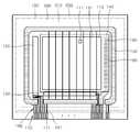
도 1은 본 발명의 실시예에 따른 유기발광 표시장치의 평면구조를 도시한 것이다. 도 1을 참조하면, 유기발광 표시장치는 TFT 어레이가 배열되는 TFT 어레이기판인 하부기판(200)과, 상기 하부기판(200)을 봉지시켜 주기위한 봉지부재인 상부기판(100)을 구비한다. 상기 하부기판(200)과 상부기판(100)은 점선으로 표시된 밀봉부(300)를 따라 도포된 시일재(310)에 의해 접합된다. 상기 시일재(310)는 실런트 또는 프릿트를 포함할 수 있다. 상기 상부기판(100)은 전면발광형 유기발광 표시장치의 경우 투명한 글래스가 사용되고, 배면발광형 유기발광 표시장치의 경우 메탈캡이 사용될 수도 있다. 또한, 상기 상부기판(100)을 사용하지 않고 필름형태의 봉지부재등이 사용될 수도 있다.1 illustrates a planar structure of an organic light emitting display device according to an exemplary embodiment of the present invention. Referring to FIG. 1, an organic light emitting display device includes a
상기 하부기판(200)의 화소영역(110)에는 다수의 화소(111)가 배열되는데, 각각 R, G, B 단위화소를 구비하는 다수의 화소(111)가 매트릭스형태로 배열된다. 화소영역(110)에 배열된 화소(111)의 R, G, B 단위화소는 도면상에는 도시되지 않았으나, 데이터신호를 스위칭 하기 위한 스위칭 트랜지스터, 상기 데이타신호에 대응하는 구동전류를 발생하는 구동 트랜지스터, 상기 데이터신호를 저장하기 위한 캐패시터 및 상기 구동전류에 따라 구동되어 소정의 화상을 표시하는 EL소자를 적어도 구비한다.A plurality of
유기발광 표시장치는 상기 화소(111)로 스캔신호를 제공하기 위한 게이트 드라이버(120)와 상기 화소(111)로 데이터신호를 제공하기 위한 데이터 드라이버(130) 그리고 캐소드버스라인(160)을 구비한다. 상기 캐소드 버스라인(160)은 화소영역(110)에 대응하여 형성된 전면전극형태의 캐소드전극(140)과 콘택(165)을 통해 연결된다. 상기 캐소드 버스라인(160)은 패드영역(170)에 배열된 패드(171)를 통해 외부로부터 제공되는 캐소드전압을 상기 캐소드전극(140)으로 제공하는 역할을 한다.The OLED display includes a
또한, 유기발광 표시장치는 화소영역(110)에 배열된 각 화소로 전원전합(Vdd)과 같은 구동전압을 제공하기 위한 구동전원 배선부(150)를 구비한다. 상기 구동전원 배선부(150)는 화소영역(110)의 외곽부에 배열되어, 각 화소로 구동전압을 제공하기 위한 다수의 구동전원라인(151)을 구비한다.In addition, the organic light emitting display device includes a driving
상기 하부기판(200)의 패드영역(170)에는 다수의 패드(171)가 배열되어, 외부로부터 소정의 신호를 상기 구동전원 배선부(150), 상기 게이트 드라이버(120), 상기 데이터 드라이버(130) 및 상기 캐소드 버스라인(160)으로 각각 제공한다. 또한, 상기 하부기판(200)의 패드 배선영역(180)에는 다수의 패드 배선라인(181)이 배열되어, 상기 패드(171)와 상기 구동전원 배선부(150), 상기 게이트 드라이버(120), 상기 데이터 드라이버(130) 및 상기 캐소드 버스라인(160)를 연결시켜 준다.A plurality of
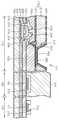
도 2는 본 발명의 실시예에 따른 유기발광 표시장치의 단면도로서, 화소영역, 패드 배선영역 및 패드영역의 요부 단면도를 도시한 것이다. 도 2에서, "110" 은 도 1의 화소영역을 나타내고, "180"은 도 1의 패드 배선영역을 나타내며, "170"은 도 1의 패드영역을 각각 나타낸다. 도 2에는 상기 화소영역(110)에 배열되는 하나의 화소(111)중 하나의 R, G, 또는 B 단위화소, 상기 패드 배선라인부(180)에 배열되는 하나의 패드 배선라인(181) 및 상기 패드부(170)에 배열된 하나의 패드(171)에 대한 단면도를 각각 도시한 것이다.2 is a cross-sectional view of an organic light emitting display device according to an exemplary embodiment of the present invention and illustrates a cross-sectional view of main parts of a pixel area, a pad wiring area, and a pad area. In FIG. 2, "110" represents the pixel region of FIG. 1, "180" represents the pad wiring region of FIG. 1, and "170" represents the pad region of FIG. 2, one R, G, or B unit pixel of one
도 2를 참조하면, 화소영역(110)에서는 하부 기판(200)상에 버퍼층(205)이 형성되고, 상기 버퍼층(205)상에 소오스/드레인영역(212), (214)과 채널영역(216)을 구비하는 반도체층(218)과, 게이트 절연막(220)상에 형성된 게이트(226)과, 층간 절연막(230)상에 상기 소오스/드레인영역(212), (214)과 콘택홀(232), (234)를 통해 연결되도록 형성되는 소오스/드레인 전극(242), (244)을 구비하는 박막 트랜지스터가 형성된다. 상기 반도체층(218)은 비정질 실리콘, 다결정 실리콘 등과 같은 실리콘층을 포함한다. 상기 실시예에서는 상기 박막 트랜지스터로 실리콘 박막 트랜지스터를 예시하였으나, 반도체층으로 유기반도체층을 사용하는 유기 박막 트랜지스터가 사용될 수 있다. 또한, 상기 박막 트랜지스터의 구조는 상기 탑 게이트 구조에 한정되는 것은 아니다.2, in the
평탄화막(250)상에는 유기 EL 소자가 형성된다. 즉, 평탄화막(250)상에는 비어홀(254)을 통해 상기 소오스/드레인 전극(242), (244)중 드레인전극(244)에 연결되는 애노드전극(265)이 형성된다. 상기 평탄화막(250)상에는 상기 애노드전극(265)의 일부분을 노출시키는 개구부(279)를 구비하는 화소분리막(270)이 형성된다. 상기 화소분리막(270)은 하부 화소분리막(271)과 상부 화소분리막(275)을 구비 한다. 상기 하부 화소분리막(271)은 무기절연막, 예를 들어 실리콘 질화막을 포함할 수 있다. 상기 상부 화소분리막(275)는 유기 절연막, 예를 들어 폴리이미드, 폴리아미드, BCB, SOG 등을 포함할 수 있다.An organic EL element is formed on the
상기 유기발광 표시장치가 전면발광구조인 경우 상기 박막 트랜지스터와 애노드 전극(265)사이에 평탄화막(250)을 포함할 수 있다. 배면발광구조인 경우에서는 상기 평탄화막(25)은 형성되지 않을 수도 있다. 따라서, 비어홀(254)를 통하지 않고 상기 드레인 전극(244)과 상기 애노드전극(265)이 직접 연결되도록 상기 층간 절연막(230)상에 상기 애노드 전극(265)이 형성되고, 상기 애노드전극(265)의 일부분이 노출되도록 상기 층간 절연막(230)상에 상기 화소분리막(270)이 형성될 수도 있다.When the organic light emitting diode display has a top emission structure, a
상기 개구부(275)내의 애노드전극(265)상에 유기막층(280)을 형성한다. 상기 유기막층(280)은 정공주입층, 정공수송층, R, G 또는 B 유기발광층, 전자수송층, 전자주입층 및 정공 차단층으로부터 선택되는 유기막층을 포함한다. 상기 유기막층(280)이 상기 화소분리막(270)의 개구부(279)내에 형성되는 것을 예시하였으나, 캐리어 수송층인 정공주입층, 정공수송층, 전자수송층, 전자주입층 및 정공 차단층 등은 화소영역(110)에 걸쳐 형성될 수도 있다. 캐소드 전극(285)이 상기 화소영역(110)에 전면전극 형태로 형성된다.The
예를 들어, 상기 유기발광 표시장치가 배면발광구조를 갖는 경우, 상기 애노드전극(265)은 투과전극을 포함하고, 상기 캐소드전극(285)은 반사전극을 포함하는 것이 바람직하다. 예를 들어, 상기 애노드전극(265)은 ITO, IZO, ZnO, 또는 In2O3 와 같은 투명도전막을 포함하고, 상기 캐소드전극(285)은 Li, Ca, LiF/Ca, LiF/Al, Al, Mg 또는 이들의 화합물 등을 포함할 수 있다. 한편, 전면발광구조를 갖는 경우에는, 상기 애노드전극(265)은 반사전극을 포함하며, 투명도전막과 반사막의 적층구조를 갖는 것이 바람직하다. 상기 애노드전극(265)은 ITO, IZO, ZnO, 또는 In2O3 등을 투명도전막을 포함하고, 반사막으로는 반사율이 우수한 금속으로 Ag, Mg, Al, Pt, Pd, Au, Ni, Nd, Ir, Cr 또는 이들의 화합물 등을 포함할 수 있다. 상기 캐소드전극(285)은 투과전극을 포함하며, 금속막과 투명도전막의 적층구조를 갖는다. 상기 캐소드전극(285)용 금속막은 Li, Ca, LiF/Ca, LiF/Al, Al, Mg 또는 이들의 화합물 등을 포함하고, 투명도전막은 ITO, IZO, ZnO, 또는 In2O3 등을 포함할 수 있다.For example, when the organic light emitting display device has a bottom light emitting structure, the
한편, 패드 배선영역(180)에서는 상기 하부기판(200)상에 버퍼층(205), 게이트 절연막(220) 및 층간 절연막(230)이 형성되고, 상기 층간 절연막(230)상에 패드 배선라인(181)이 형성되고, 상기 패드 배선라인(181)을 덮도록 상기 층간 절연막(230)상에 제1절연막(272)이 형성된다. 상기 패드 배선라인(181)이 상기 층간 절연막(230)상에 배열되는 것을 예시하였으나, 상기 버퍼층(205)이나 상기 게이트 절연막(230)상에 형성될 수도 있다. 상기 패드 배선라인(181)은 상기 박막 트랜지스터의 전극물질중 적어도 하나를 포함할 수 있다. 상기 패드 배선라인(181)이 단일층으로 구성되는 것을 예시하였으나, 다층막을 포함할 수도 있다. 상기 제1절연막(272)은 상기 하부 화소분리막(271)과 동일한 물질로 이루어진다. 상기 제1절연막(272)은 실리콘 질화막과 같은 무기절연막을 포함할 수 있다. 상기 제1절연 막(272)과 상기 층간 절연막(230)상에 시일재(310)가 도포된다.Meanwhile, in the
상기 패드영역(170)에서는 상기 하부기판(200)상에 버퍼층(205), 게이트 절연막(220) 및 층간 절연막(230)이 형성되고, 상기 층간 절연막(230)상에 패드(171)가 형성되고, 상기 패드(171)를 덮도록 상기 층간 절연막(230)상에 제2절연막(273)이 형성된다. 상기 패드(171)가 상기 층간 절연막(230)상에 배열되는 것을 예시하였으나, 상기 버퍼층(205)이나 상기 게이트 절연막(230)상에 형성될 수도 있다. 상기 패드(171)는 상기 박막 트랜지스터의 전극물질중 적어도 하나를 포함할 수 있다. 상기 패드(171)는 단일층으로 구성되는 것을 예시하였으나, 다층막을 포함할 수도 있다. 상기 제2절연막(273)은 상기 하부 화소분리막과 동일한 물질로 이루어진다. 상기 제2절연막(273)은 실리콘 질화막과 같은 무기 절연막을 포함할 수 있다. 상기 제2절연막(274)은 상기 패드(171)의 일부분을 노출시키는 개구부(274)를 구비한다.In the
도 3a 내지 도 3g는 본 발명의 실시예에 따른 유기발광 표시장치의 제조방법을 설명하기 위한 단면도를 도시한 것이다.3A to 3G are cross-sectional views illustrating a method of manufacturing an organic light emitting display device according to an embodiment of the present invention.
도 3a를 참조하면, 하부기판(200)이 마련된다. 상기 하부기판(200)은 화소영역(110), 패드 배선영역(180) 및 패드영역(170)을 구비한다. 도면상에는 도시되지 않았으나, 상기 화소영역(110)에는 도 2에 도시된 바와 같이, 버퍼층(205)상에 형성된 반도체층(218), 게이트 절연막(220)상에 형성된 게이트(226) 및 층간 절연막(230)상에 형성된 소오스 및 드레인 전극(242, 244)을 구비하는 박막 트랜지스터가 형성되어 있다. 상기 박막 트랜지스터를 포함하는 상기 하부기판(200)상에는 평 탄화막(250)이 형성되고, 상기 평탄화막(250)상에 애노드전극(265)이 형성되어 비어홀(254)을 통해 상기 드레인 전극(244)에 연결되어 있다.Referring to FIG. 3A, a
한편, 상기 패드 배선영역(180)에는 상기 박막 트랜지스터의 상기 게이트(226), 상기 소오스 및 드레인 전극(242, 244) 또는/및 상기 애노드전극(265)을 형성할 때 형성되는 패드 배선라인(181)이 상기 하부기판(200)상에 형성된다. 상기 패드 배선라인(181)과 상기 하부기판(200)사이에는 버퍼층(205), 게이트 절연막(220) 및 층간 절연막(230) 등이 배열될 수도 있다.In the
또한, 상기 패드영역(170)에는 상기 박막 트랜지스터의 상기 게이트(226), 상기 소오스 및 드레인 전극(242, 244) 또는/및 상기 애노드전극(265)을 형성할 때 형성되는 패드(171)가 상기 하부기판(200)상에 형성된다. 상기 패드(171)와 상기 하부기판(200)사이에는 버퍼층(205), 게이트 절연막(220) 및 층간 절연막(230) 등이 배열될 수도 있다. 상기 패드(171)는 상기 패드 배선라인(181)과 동일한 물질로 이루어질 수 있다.In the
도 3b를 참조하면, 상기 화소영역(110)의 상기 애노드전극(265), 상기 패드 배선영역(180)의 상기 패드 배선라인(181) 및 상기 패드영역(170)의 상기 패드(171)를 포함하는 상기 하부기판(200)상에 무기 절연막(270a)과 유기 절연막(275a)을 순차 형성한다. 상기 무기 절연막(270a)은 실리콘 질화막을 포함할 수 있다. 상기 유기 절연막(275a)은 폴리이미드, 폴리아미드, BCB, SOG 등을 포함할 수 있다.Referring to FIG. 3B, the
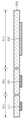
도 3c를 참조하면, 상기 유기 절연막(275a)상에 감광막을 도포한 다음, 하프 톤 마스크(10)를 이용하여 상기 감광막을 패터닝한다. 상기 하프톤 마스크(10)는 기판(11)과 상기 기판(11)상에 배열된 불투과패턴(12), 반투과패턴(13) 및 개구영역(14)을 구비한다. 상기 불투과패턴(12)은 입사되는 광을 전혀 투과시키지 않는 것으로서, 상기 화소영역(110)에 대응하여 배열되고, 상기 반투과패턴(13)은 입사되는 광을 부분적으로 투과시키는 것으로서, 상기 패드 배선영역(180) 및 상기 패드영역(170)의 일부분에 대응하여 배열된다. 상기 개구영역(14)은 입사되는 광을 모두 투과시키는 것으로서, 상기 화소영역(110)의 상기 애노드 전극(165)이 노출될 부분과 상기 패드영역(170)의 상기 패드(171)가 노출될 부분에 대응하여 배열된다.Referring to FIG. 3C, a photoresist film is coated on the organic insulating
따라서, 상기 하프톤 마스크(10)를 이용하여 상기 감광막을 패터닝하면, 제1감광막 패턴(291), 제2감광막 패턴(293) 및 제3감광막 패턴(294)이 형성된다. 상기 제1감광막 패턴(291)은 후속의 식각공정에서 상기 애노드전극(265)에 대응하는 부분에서는 유기 절연막(275a)이 완전히 제거되도록 개구부(292)를 구비하고, 나머지 부분에서는 상기 유기 절연막(275a)이 식각되지 않을 정도로 두꺼운 제1두께를 갖도록 상기 화소영역(110)에 배열된다. 상기 제2감광막 패턴(293)은 후속의 식각공정에서 그 하부의 유기 절연막(275a)이 부분적으로 식각되도록 상기 제1두께보다 얇은 제2두께를 갖도록 상기 패드 배선영역(180)에 배열된다. 상기 제3감광막 패턴(294)은 후속의 식각공정에서 상기 패드(171)가 노출될 부분에서는 상기 유기 절연막(275a)이 완전히 제거되도록 개구부(295)를 구비하고, 나머지 부분에서는 상기 유기절연막(275a)이 부분적으로 식각되도록 상기 제2두께를 갖도록 상기 패드영역(170)에 배열된다.Accordingly, when the photoresist layer is patterned using the
도 3d를 참조하면, 상기 제1 내지 제3감광막 패턴(291, 293, 294)을 이용하여 상기 유기 절연막(275a)을 패터닝하면, 상기 화소영역(110)에서는 상기 애노드전극(265)에 대응하는 상기 무기 절연막(270a)이 노출되도록 개구부(279a)를 구비하는 제1유기절연막 패턴(275)이 형성되고, 상기 패드 배선영역(180)에서는 제2유기 절연막 패턴(276)이 형성되며, 상기 패드영역(170)에서는 상기 패드(171)에 대응하는 상기 무기 절연막(270a)상에 형성하되, 상기 패드(171)가 노출될 부분에 대응하여 개구부(278)를 구비하는 제3유기 절연막 패턴(277)이 형성된다.Referring to FIG. 3D, when the organic insulating
도 3e를 참조하면, 상기 제1 내지 제3유기 절연막 패턴(275, 276, 277)을 마스크로 이용하여 노출된 무기 절연막(270a)을 식각하여 상기 화소영역(110)에는 개구부(279)를 구비하는 화소분리막(270)을 형성한다. 상기 화소분리막(270)은 제1무기 절연막 패턴(271)과 제1유기 절연막 패턴(275)을 구비하되, 상기 개구부(279)가 상기 제1무기 절연막 패턴(271)과 상기 제1유기 절연막 패턴(275)에 걸쳐 형성되어 상기 애노드 전극(265)의 일부분을 노출시켜 준다. 또한, 상기 패드 배선영역(180)에서는 상기 패드 배선라인(181)을 덮도록 제2무기 절연막 패턴(272)이 형성되고, 상기 패드영역(170)에서는 상기 패드(171)의 일부분을 노출시켜 주는 개구부(274)를 구비하는 제3무기 절연막 패턴(273)이 형성된다.Referring to FIG. 3E, the exposed inorganic insulating
도 3f를 참조하면, 상기 패드 배선영역(180)의 제2유기 절연막 패턴(276)과 상기 패드영역(170)의 제3유기 절연막 패턴(277)을 O2 애싱방법, 케미컬을 이용한 식각방법 또는 노광 및 현상 방법 등을 이용하여 제거한다. 이때, 상기 화소영역(110)의 상기 제1유기 절연막 패턴(275)도 부분적을 식각될 수 있다. 따라서, 상 기 도 3b의 유기 절연막 형성공정에서 도 3f의 식각량을 고려하여 상기 유기 절연막(275a)의 두께를 결정할 수 있다.Referring to FIG. 3F, the second organic insulating
도 3g를 참조하면, 상기 화소영역(110)에 유기막(280)을 형성하고 캐소드전극(285)을 형성한다. 이어서, 상기 패드 배선영역(180)의 상기 제2무기절연막 패턴(272)중 밀봉부(300)에 대응하는 부분에 시일재(310)를 도포한 다음 도 1과 같이 상기 상부기판(100)을 접합시켜 상기 상, 하부 기판(100, 200)의 화소영역(110)에 배열된 화소(111)들을 밀봉시켜 준다. 상기 시일재(310)는 실런트 또는 프릿트를 포함할 수 있다. 따라서, 유기발광 표시장치가 얻어진다.Referring to FIG. 3G, an
상기한 바와같은 본 발명의 실시예에 따르면, 무기 절연막과 유기 절연막으로 구성된 화소분리막, 패드 및 패드배선라인을 절연시켜 주기 위한 무기 절연막을 한번의 마스크공정을 통해 형성하여 줌으로써 공정을 단순화하고, 애노드전극과 봉지부재사이에 질화막으로 된 패시베이션막을 형성하여 줌으로써 EL 소자의 장수명화 및 신뢰성 향상을 도모하고, 패드의 불량을 방지할 수 있다.According to the embodiment of the present invention as described above, by simplifying the process by forming an inorganic insulating film for insulating the pixel isolation film, pad and pad wiring line consisting of an inorganic insulating film and an organic insulating film through a single mask process, the anode By forming a passivation film made of a nitride film between the electrode and the sealing member, the life of the EL element can be extended and the reliability can be improved, and the failure of the pad can be prevented.
상기에서는 본 발명의 바람직한 실시예를 참조하여 설명하였지만, 해당 기술분야의 숙련된 당업자는 하기의 특허청구범위에 기재된 본 발명의 사상 및 영역으로부터 벗어나지 않는 범위내에서 본 발명을 다양하게 수정 및 변경시킬 수 있음을 이해할 수 있을 것이다.Although the above has been described with reference to a preferred embodiment of the present invention, those skilled in the art will be able to variously modify and change the present invention without departing from the spirit and scope of the invention as set forth in the claims below. It will be appreciated.
Claims (18)
Translated fromKoreanPriority Applications (2)
| Application Number | Priority Date | Filing Date | Title |
|---|---|---|---|
| KR1020070026187AKR100838082B1 (en) | 2007-03-16 | 2007-03-16 | OLED display device and manufacturing method |
| US11/892,008US7663311B2 (en) | 2007-03-16 | 2007-08-17 | Organic light emitting display (OLED) device and method of fabricating the same |
Applications Claiming Priority (1)
| Application Number | Priority Date | Filing Date | Title |
|---|---|---|---|
| KR1020070026187AKR100838082B1 (en) | 2007-03-16 | 2007-03-16 | OLED display device and manufacturing method |
Publications (1)
| Publication Number | Publication Date |
|---|---|
| KR100838082B1true KR100838082B1 (en) | 2008-06-16 |
Family
ID=39761972
Family Applications (1)
| Application Number | Title | Priority Date | Filing Date |
|---|---|---|---|
| KR1020070026187AActiveKR100838082B1 (en) | 2007-03-16 | 2007-03-16 | OLED display device and manufacturing method |
Country Status (2)
| Country | Link |
|---|---|
| US (1) | US7663311B2 (en) |
| KR (1) | KR100838082B1 (en) |
Cited By (4)
| Publication number | Priority date | Publication date | Assignee | Title |
|---|---|---|---|---|
| US8637333B2 (en) | 2010-12-30 | 2014-01-28 | Samsung Display Co., Ltd. | Organic light emitting diode display and manufacturing method of the same |
| KR20150012203A (en)* | 2013-07-24 | 2015-02-03 | 삼성디스플레이 주식회사 | An organic emitting display apparatus and the manufacturing method thereof |
| KR101873448B1 (en)* | 2011-07-15 | 2018-07-03 | 삼성디스플레이 주식회사 | Organinc light emitting display device and manufacturing method for the same |
| KR20200046196A (en)* | 2018-10-23 | 2020-05-07 | 삼성디스플레이 주식회사 | Display device and method of manufacturing the same |
Families Citing this family (27)
| Publication number | Priority date | Publication date | Assignee | Title |
|---|---|---|---|---|
| KR101582937B1 (en)* | 2008-12-02 | 2016-01-08 | 삼성디스플레이 주식회사 | Organic light emitting diode display and method for manufacturing the same |
| KR20110024531A (en)* | 2009-09-02 | 2011-03-09 | 삼성모바일디스플레이주식회사 | Organic light emitting display device |
| US20110163663A1 (en)* | 2010-01-07 | 2011-07-07 | Samsung Mobile Display Co., Ltd. | Organic Light Emitting Display Device and Method of Making the Same |
| KR101084198B1 (en)* | 2010-02-24 | 2011-11-17 | 삼성모바일디스플레이주식회사 | Organic light emitting display |
| US8460747B2 (en) | 2010-03-04 | 2013-06-11 | Guardian Industries Corp. | Large-area transparent conductive coatings including alloyed carbon nanotubes and nanowire composites, and methods of making the same |
| US8604332B2 (en) | 2010-03-04 | 2013-12-10 | Guardian Industries Corp. | Electronic devices including transparent conductive coatings including carbon nanotubes and nanowire composites, and methods of making the same |
| US8518472B2 (en)* | 2010-03-04 | 2013-08-27 | Guardian Industries Corp. | Large-area transparent conductive coatings including doped carbon nanotubes and nanowire composites, and methods of making the same |
| KR20120032250A (en)* | 2010-09-28 | 2012-04-05 | 삼성모바일디스플레이주식회사 | Flat panel display apparatus and method of manufacturing the same |
| KR101807849B1 (en)* | 2010-12-08 | 2017-12-12 | 삼성디스플레이 주식회사 | Organinc light emitting display device and manufacturing method for the same |
| US20130005139A1 (en) | 2011-06-30 | 2013-01-03 | Guardian Industries Corp. | Techniques for manufacturing planar patterned transparent contact and/or electronic devices including same |
| US8747959B2 (en) | 2011-06-30 | 2014-06-10 | Guardian Industries Corp. | Planar patterned transparent contact, devices with planar patterned transparent contacts, and/or methods of making the same |
| US20130005135A1 (en) | 2011-06-30 | 2013-01-03 | Guardian Industries Corp. | Planar patterned transparent contact, devices with planar patterned transparent contacts, and/or methods of making the same |
| US8497155B1 (en) | 2012-06-05 | 2013-07-30 | Guardian Industries Corp. | Planarized TCO-based anode for OLED devices, and/or methods of making the same |
| US8608525B1 (en) | 2012-06-05 | 2013-12-17 | Guardian Industries Corp. | Coated articles and/or devices with optical out-coupling layer stacks (OCLS), and/or methods of making the same |
| US8524526B1 (en) | 2012-08-14 | 2013-09-03 | Guardian Industries Corp. | Organic light emitting diode with transparent electrode and method of making same |
| US8766245B2 (en) | 2012-08-14 | 2014-07-01 | Guardian Industries Corp. | Organic light emitting diode with transparent electrode and method of making same |
| US9263701B2 (en) | 2013-03-14 | 2016-02-16 | Guardian Industries Corp. | Coated article and/or device with optical out-coupling layer stack (OCLS) including vacuum deposited index match layer over scattering matrix, and/or associated methods |
| EP2963701B1 (en) | 2013-09-30 | 2020-05-06 | LG Display Co., Ltd. | Method for manufacturing an organic electronic device |
| KR102384650B1 (en)* | 2015-04-14 | 2022-04-11 | 삼성디스플레이 주식회사 | Organic light-emitting display apparatus and manufacturing the same |
| KR102500273B1 (en)* | 2015-10-19 | 2023-02-16 | 삼성디스플레이 주식회사 | Ddisplay apparatus |
| US11148228B2 (en) | 2017-07-10 | 2021-10-19 | Guardian Glass, LLC | Method of making insulated glass window units |
| US10987902B2 (en) | 2017-07-10 | 2021-04-27 | Guardian Glass, LLC | Techniques for laser ablation/scribing of coatings in pre- and post-laminated assemblies, and/or associated methods |
| JP6906397B2 (en)* | 2017-08-10 | 2021-07-21 | 株式会社ジャパンディスプレイ | Display device |
| KR102577043B1 (en)* | 2017-12-11 | 2023-09-08 | 엘지디스플레이 주식회사 | Electroluminescent display device |
| JP6983084B2 (en)* | 2018-02-07 | 2021-12-17 | 株式会社ジャパンディスプレイ | Organic EL display device |
| CN109378409B (en)* | 2018-10-18 | 2020-04-14 | 纳晶科技股份有限公司 | Electroluminescent device and manufacturing method thereof |
| CN114758586B (en)* | 2022-04-22 | 2023-12-29 | 京东方科技集团股份有限公司 | Test element group, display panel, manufacturing method of display panel and test method of display panel |
Citations (4)
| Publication number | Priority date | Publication date | Assignee | Title |
|---|---|---|---|---|
| JP2008001003A (en)* | 2006-06-23 | 2008-01-10 | Konica Minolta Holdings Inc | Inkjet image recording method |
| JP2008005004A (en)* | 2006-06-20 | 2008-01-10 | Fujitsu Ltd | Communications system |
| JP2008005005A (en)* | 2006-06-20 | 2008-01-10 | Denso Corp | Sample-and-hold circuit |
| JP2008006003A (en)* | 2006-06-28 | 2008-01-17 | Tiger Vacuum Bottle Co Ltd | Attachment for chopper function of cooking mixer |
Family Cites Families (9)
| Publication number | Priority date | Publication date | Assignee | Title |
|---|---|---|---|---|
| US5294869A (en)* | 1991-12-30 | 1994-03-15 | Eastman Kodak Company | Organic electroluminescent multicolor image display device |
| JP2666103B2 (en)* | 1992-06-03 | 1997-10-22 | カシオ計算機株式会社 | Thin film semiconductor device |
| JP4472056B2 (en) | 1999-07-23 | 2010-06-02 | 株式会社半導体エネルギー研究所 | Electroluminescence display device and manufacturing method thereof |
| KR100441433B1 (en)* | 2001-04-12 | 2004-07-22 | 삼성에스디아이 주식회사 | flat panel display device and method for fabricating thereof |
| KR100552975B1 (en) | 2003-11-22 | 2006-02-15 | 삼성에스디아이 주식회사 | Active matrix organic light emitting display device and manufacturing method thereof |
| KR100611152B1 (en) | 2003-11-27 | 2006-08-09 | 삼성에스디아이 주식회사 | Flat Panel Display |
| KR101035914B1 (en)* | 2004-07-30 | 2011-05-23 | 엘지디스플레이 주식회사 | Flat panel display device and manufacturing method thereof |
| KR100683684B1 (en) | 2004-10-28 | 2007-02-20 | 삼성에스디아이 주식회사 | Organic light emitting display device having organic thin film transistor |
| WO2007114536A1 (en)* | 2006-04-05 | 2007-10-11 | Daewoo Electronics Corporation | Organic electroluminescence device and method for manufacturing same |
- 2007
- 2007-03-16KRKR1020070026187Apatent/KR100838082B1/enactiveActive
- 2007-08-17USUS11/892,008patent/US7663311B2/enactiveActive
Patent Citations (4)
| Publication number | Priority date | Publication date | Assignee | Title |
|---|---|---|---|---|
| JP2008005004A (en)* | 2006-06-20 | 2008-01-10 | Fujitsu Ltd | Communications system |
| JP2008005005A (en)* | 2006-06-20 | 2008-01-10 | Denso Corp | Sample-and-hold circuit |
| JP2008001003A (en)* | 2006-06-23 | 2008-01-10 | Konica Minolta Holdings Inc | Inkjet image recording method |
| JP2008006003A (en)* | 2006-06-28 | 2008-01-17 | Tiger Vacuum Bottle Co Ltd | Attachment for chopper function of cooking mixer |
Non-Patent Citations (4)
| Title |
|---|
| 공개특허 제2001-0039733호 |
| 공개특허 제2005-0049693호 |
| 공개특허 제2005-0051076호 |
| 공개특허 제2006-0037730호 |
Cited By (13)
| Publication number | Priority date | Publication date | Assignee | Title |
|---|---|---|---|---|
| US8637333B2 (en) | 2010-12-30 | 2014-01-28 | Samsung Display Co., Ltd. | Organic light emitting diode display and manufacturing method of the same |
| US9312316B2 (en) | 2010-12-30 | 2016-04-12 | Samsung Display Co., Ltd. | Organic light emitting diode display and manufacturing method of the same |
| KR101873448B1 (en)* | 2011-07-15 | 2018-07-03 | 삼성디스플레이 주식회사 | Organinc light emitting display device and manufacturing method for the same |
| KR20210013636A (en)* | 2013-07-24 | 2021-02-04 | 삼성디스플레이 주식회사 | An organic light emitting display apparatus and the manufacturing method thereof |
| KR102210987B1 (en) | 2013-07-24 | 2021-02-04 | 삼성디스플레이 주식회사 | An organic emitting display apparatus and the manufacturing method thereof |
| KR20150012203A (en)* | 2013-07-24 | 2015-02-03 | 삼성디스플레이 주식회사 | An organic emitting display apparatus and the manufacturing method thereof |
| KR102322017B1 (en) | 2013-07-24 | 2021-11-09 | 삼성디스플레이 주식회사 | An organic light emitting display apparatus and the manufacturing method thereof |
| KR20210135436A (en)* | 2013-07-24 | 2021-11-15 | 삼성디스플레이 주식회사 | An organic light emitting display apparatus and the manufacturing method thereof |
| KR102367275B1 (en) | 2013-07-24 | 2022-02-25 | 삼성디스플레이 주식회사 | An organic light emitting display apparatus and the manufacturing method thereof |
| US11296175B2 (en) | 2013-07-24 | 2022-04-05 | Samsung Display Co., Ltd. | Organic light-emitting display apparatus and manufacturing method thereof |
| KR20200046196A (en)* | 2018-10-23 | 2020-05-07 | 삼성디스플레이 주식회사 | Display device and method of manufacturing the same |
| US12082479B2 (en) | 2018-10-23 | 2024-09-03 | Samsung Display Co., Ltd. | Display device and method of manufacturing the same |
| KR102711652B1 (en)* | 2018-10-23 | 2024-10-02 | 삼성디스플레이 주식회사 | Display device and method of manufacturing the same |
Also Published As
| Publication number | Publication date |
|---|---|
| US20080224600A1 (en) | 2008-09-18 |
| US7663311B2 (en) | 2010-02-16 |
Similar Documents
| Publication | Publication Date | Title |
|---|---|---|
| KR100838082B1 (en) | OLED display device and manufacturing method | |
| US10541288B2 (en) | Flexible organic electroluminescent device and method for fabricating the same | |
| KR100427883B1 (en) | Self light emitting display panel and meth od for manufacturing the same | |
| KR101073552B1 (en) | Organic light emitting diode display and method of manufacturing the same | |
| US8241933B2 (en) | Organic light emitting diode display and method of manufacturing the same | |
| US9312319B2 (en) | Organic light emitting diode device and method for fabricating the same | |
| US7741640B2 (en) | Top-emission organic light-emitting display device | |
| JP5323667B2 (en) | Organic electroluminescent device and manufacturing method thereof | |
| KR101305377B1 (en) | Top emission type organic electroluminescent device and method of fabricating the same | |
| JP4809087B2 (en) | ELECTROLUMINESCENT DEVICE, ELECTRONIC DEVICE, AND METHOD FOR MANUFACTURING ELECTROLUMINESCENT DEVICE | |
| KR101927334B1 (en) | Organic electro luminescence device and method for fabricating the same | |
| KR101525804B1 (en) | Organic light emitting device and manufacturing method thereof | |
| US20090066236A1 (en) | Organic light-emitting display device and method of manufacturing the same | |
| KR20220151137A (en) | Electroluminescent display device | |
| JP2004193129A (en) | Organic light-emitting display panel | |
| KR20100068644A (en) | Top emission type organic electro luminescent device and method of fabricating the same | |
| KR20140146426A (en) | Display device and method for manufacturing display device | |
| KR20150134953A (en) | Organic light emitting diode display device and the emthod fof fabricating the same | |
| KR20100125502A (en) | Organic light emitting display device and manufacturing method | |
| US9911802B2 (en) | Display device and method for manufacturing the same | |
| KR101480005B1 (en) | Organic light emitting display and manufacturing method thereof | |
| KR101996438B1 (en) | Substrate for display device, display device and method of manufacturing the same | |
| JP2001100655A (en) | El display device | |
| JP4127608B2 (en) | Self-luminous display panel | |
| KR20150010037A (en) | Display device and method of fabricating the same |
Legal Events
| Date | Code | Title | Description |
|---|---|---|---|
| A201 | Request for examination | ||
| PA0109 | Patent application | Patent event code:PA01091R01D Comment text:Patent Application Patent event date:20070316 | |
| PA0201 | Request for examination | ||
| E902 | Notification of reason for refusal | ||
| PE0902 | Notice of grounds for rejection | Comment text:Notification of reason for refusal Patent event date:20080131 Patent event code:PE09021S01D | |
| E701 | Decision to grant or registration of patent right | ||
| PE0701 | Decision of registration | Patent event code:PE07011S01D Comment text:Decision to Grant Registration Patent event date:20080423 | |
| GRNT | Written decision to grant | ||
| PR0701 | Registration of establishment | Comment text:Registration of Establishment Patent event date:20080609 Patent event code:PR07011E01D | |
| PR1002 | Payment of registration fee | Payment date:20080610 End annual number:3 Start annual number:1 | |
| PG1601 | Publication of registration | ||
| PR1001 | Payment of annual fee | Payment date:20110527 Start annual number:4 End annual number:4 | |
| PR1001 | Payment of annual fee | Payment date:20120601 Start annual number:5 End annual number:5 | |
| FPAY | Annual fee payment | Payment date:20130530 Year of fee payment:6 | |
| PR1001 | Payment of annual fee | Payment date:20130530 Start annual number:6 End annual number:6 | |
| FPAY | Annual fee payment | Payment date:20140530 Year of fee payment:7 | |
| PR1001 | Payment of annual fee | Payment date:20140530 Start annual number:7 End annual number:7 | |
| FPAY | Annual fee payment | Payment date:20150601 Year of fee payment:8 | |
| PR1001 | Payment of annual fee | Payment date:20150601 Start annual number:8 End annual number:8 | |
| FPAY | Annual fee payment | Payment date:20160530 Year of fee payment:9 | |
| PR1001 | Payment of annual fee | Payment date:20160530 Start annual number:9 End annual number:9 | |
| FPAY | Annual fee payment | Payment date:20170601 Year of fee payment:10 | |
| PR1001 | Payment of annual fee | Payment date:20170601 Start annual number:10 End annual number:10 | |
| FPAY | Annual fee payment | Payment date:20190529 Year of fee payment:12 | |
| PR1001 | Payment of annual fee | Payment date:20190529 Start annual number:12 End annual number:12 | |
| PR1001 | Payment of annual fee | Payment date:20200527 Start annual number:13 End annual number:13 | |
| PR1001 | Payment of annual fee | Payment date:20210601 Start annual number:14 End annual number:14 | |
| PR1001 | Payment of annual fee | Payment date:20220523 Start annual number:15 End annual number:15 | |
| PR1001 | Payment of annual fee | Payment date:20240523 Start annual number:17 End annual number:17 |