KR100833596B1 - Semiconductor device and its layout method - Google Patents
Semiconductor device and its layout methodDownload PDFInfo
- Publication number
- KR100833596B1 KR100833596B1KR1020070042244AKR20070042244AKR100833596B1KR 100833596 B1KR100833596 B1KR 100833596B1KR 1020070042244 AKR1020070042244 AKR 1020070042244AKR 20070042244 AKR20070042244 AKR 20070042244AKR 100833596 B1KR100833596 B1KR 100833596B1
- Authority
- KR
- South Korea
- Prior art keywords
- conductive lines
- layer
- lines
- interface
- circuit blocks
- Prior art date
- Legal status (The legal status is an assumption and is not a legal conclusion. Google has not performed a legal analysis and makes no representation as to the accuracy of the status listed.)
- Expired - Fee Related
Links
Images


Classifications
- G—PHYSICS
- G11—INFORMATION STORAGE
- G11C—STATIC STORES
- G11C11/00—Digital stores characterised by the use of particular electric or magnetic storage elements; Storage elements therefor
- G11C11/21—Digital stores characterised by the use of particular electric or magnetic storage elements; Storage elements therefor using electric elements
- G11C11/34—Digital stores characterised by the use of particular electric or magnetic storage elements; Storage elements therefor using electric elements using semiconductor devices
- G11C11/40—Digital stores characterised by the use of particular electric or magnetic storage elements; Storage elements therefor using electric elements using semiconductor devices using transistors
- G11C11/401—Digital stores characterised by the use of particular electric or magnetic storage elements; Storage elements therefor using electric elements using semiconductor devices using transistors forming cells needing refreshing or charge regeneration, i.e. dynamic cells
- G11C11/4063—Auxiliary circuits, e.g. for addressing, decoding, driving, writing, sensing or timing
- G11C11/407—Auxiliary circuits, e.g. for addressing, decoding, driving, writing, sensing or timing for memory cells of the field-effect type
- G11C11/409—Read-write [R-W] circuits
- G11C11/4093—Input/output [I/O] data interface arrangements, e.g. data buffers
- G—PHYSICS
- G11—INFORMATION STORAGE
- G11C—STATIC STORES
- G11C11/00—Digital stores characterised by the use of particular electric or magnetic storage elements; Storage elements therefor
- G11C11/21—Digital stores characterised by the use of particular electric or magnetic storage elements; Storage elements therefor using electric elements
- G11C11/34—Digital stores characterised by the use of particular electric or magnetic storage elements; Storage elements therefor using electric elements using semiconductor devices
- G11C11/40—Digital stores characterised by the use of particular electric or magnetic storage elements; Storage elements therefor using electric elements using semiconductor devices using transistors
- G11C11/401—Digital stores characterised by the use of particular electric or magnetic storage elements; Storage elements therefor using electric elements using semiconductor devices using transistors forming cells needing refreshing or charge regeneration, i.e. dynamic cells
- G11C11/4063—Auxiliary circuits, e.g. for addressing, decoding, driving, writing, sensing or timing
- G11C11/407—Auxiliary circuits, e.g. for addressing, decoding, driving, writing, sensing or timing for memory cells of the field-effect type
- G11C11/409—Read-write [R-W] circuits
- G11C11/4091—Sense or sense/refresh amplifiers, or associated sense circuitry, e.g. for coupled bit-line precharging, equalising or isolating
- G—PHYSICS
- G11—INFORMATION STORAGE
- G11C—STATIC STORES
- G11C11/00—Digital stores characterised by the use of particular electric or magnetic storage elements; Storage elements therefor
- G11C11/21—Digital stores characterised by the use of particular electric or magnetic storage elements; Storage elements therefor using electric elements
- G11C11/34—Digital stores characterised by the use of particular electric or magnetic storage elements; Storage elements therefor using electric elements using semiconductor devices
- G11C11/40—Digital stores characterised by the use of particular electric or magnetic storage elements; Storage elements therefor using electric elements using semiconductor devices using transistors
- G11C11/401—Digital stores characterised by the use of particular electric or magnetic storage elements; Storage elements therefor using electric elements using semiconductor devices using transistors forming cells needing refreshing or charge regeneration, i.e. dynamic cells
- G11C11/4063—Auxiliary circuits, e.g. for addressing, decoding, driving, writing, sensing or timing
- G11C11/407—Auxiliary circuits, e.g. for addressing, decoding, driving, writing, sensing or timing for memory cells of the field-effect type
- G11C11/409—Read-write [R-W] circuits
- G11C11/4097—Bit-line organisation, e.g. bit-line layout, folded bit lines
- G—PHYSICS
- G11—INFORMATION STORAGE
- G11C—STATIC STORES
- G11C5/00—Details of stores covered by group G11C11/00
- G11C5/02—Disposition of storage elements, e.g. in the form of a matrix array
- G11C5/025—Geometric lay-out considerations of storage- and peripheral-blocks in a semiconductor storage device
- G—PHYSICS
- G11—INFORMATION STORAGE
- G11C—STATIC STORES
- G11C7/00—Arrangements for writing information into, or reading information out from, a digital store
- G11C7/06—Sense amplifiers; Associated circuits, e.g. timing or triggering circuits
- G—PHYSICS
- G11—INFORMATION STORAGE
- G11C—STATIC STORES
- G11C7/00—Arrangements for writing information into, or reading information out from, a digital store
- G11C7/18—Bit line organisation; Bit line lay-out
Landscapes
- Engineering & Computer Science (AREA)
- Microelectronics & Electronic Packaging (AREA)
- Computer Hardware Design (AREA)
- Semiconductor Memories (AREA)
- Dram (AREA)
Abstract
Translated fromKoreanDescription
Translated fromKorean도 1은 종래의 반도체 장치의 레이아웃 구조의 일 예를 나타내는 도면.1 is a diagram illustrating an example of a layout structure of a conventional semiconductor device.
도 2는 종래의 반도체 장치의 레이아웃 구조의 다른 예를 나타내는 도면.2 is a diagram showing another example of a layout structure of a conventional semiconductor device.
도 3은 종래의 반도체 장치의 레이아웃 구조의 또 다른 예를 나타내는 도면.3 is a view showing still another example of the layout structure of a conventional semiconductor device.
도 4는 종래의 반도체 장치의 코어 영역의 레이아웃 구조를 나타내는 도면.4 shows a layout structure of a core region of a conventional semiconductor device.
도 5는 본 발명의 제 1 실시 예에 따른 반도체 장치의 레이아웃 구조를 나타내는 도면.5 is a diagram illustrating a layout structure of a semiconductor device in accordance with a first embodiment of the present invention.
도 6은 본 발명의 제 2 실시 예에 따른 반도체 장치의 레이아웃 구조를 나타내는 도면.6 illustrates a layout structure of a semiconductor device in accordance with a second embodiment of the present invention.
도 7은 본 발명의 제 3 실시 예에 따른 반도체 장치의 레이아웃 구조를 나타내는 도면.7 illustrates a layout structure of a semiconductor device in accordance with a third embodiment of the present invention.
도 8은 본 발명의 반도체 장치에서 서로 다른 층에 형성되는 라인들의 배치의 일 예를 나타내는 도면.8 is a view showing an example of arrangement of lines formed in different layers in the semiconductor device of the present invention.
본 발명은 반도체 장치에 관한 것으로, 더욱 상세하게는 다층 구조의 라인 메쉬를 포함하는 반도체 장치에 관한 것이다.The present invention relates to a semiconductor device, and more particularly, to a semiconductor device including a line mesh of a multilayer structure.
일반적으로, 반도체 장치를 설계할 때 회로 배치도 중요하지만 라인 설계도 무척 중요하다. 라인 설계를 어떻게 하느냐에 따라서 라인 간의 로딩 또는 커플링 발생 여부가 결정되므로, 회로 설계에서 요구되는 신호 라인과 같은 라인 설계에 많은 주의가 필요하다.In general, circuit layout is important when designing semiconductor devices, but line design is also very important. How to design a line determines whether loading or coupling between lines occurs, so much care must be taken in line design, such as signal lines required in circuit design.
또한, 반도체 공정이 점점 미세화되면서 회로를 배치를 공간이 점점 부족해지며, 특히, 최근 반도체 공정은 소자들이 차지하는 레이아웃 면적보다 라인이 차지하는 레이아웃 면적이 더 크므로, 레이아웃 면적을 줄이기 위해 라인을 효율적으로 배치하는 것이 중요하다.In addition, as the semiconductor process becomes smaller and smaller, space for arranging circuits becomes increasingly scarce, and in particular, in recent semiconductor processes, since the layout area occupied by the line is larger than the layout area occupied by the devices, the line is efficiently arranged to reduce the layout area. It is important to do.
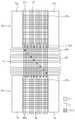
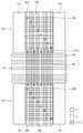
한편, 종래의 반도체 장치는 도 1 내지 도 3과 같이 다양한 라인 레이아웃 구조를 가질 수 있다.Meanwhile, the conventional semiconductor device may have various line layout structures as shown in FIGS. 1 to 3.
도 1 내지 도 3을 참조하면, 종래의 반도체 장치는 다수의 유닛 셀(10a,10b)과 글로벌 입출력 영역(18)을 포함하는 구조를 갖는다. 여기서, 각 유닛 셀(예컨대, 10a)은 두 회로 블럭(12a,14a)과, 두 회로 블럭(12a,14a) 사이에 배치되는 라인 메쉬(16a)를 한정하는 영역을 의미한다.1 to 3, a conventional semiconductor device has a structure including a plurality of
도 1 내지 도 3에서, 도면 부호 'L1~L3'은 서로 다른 층(layer)을 의미하고, 도면 부호 'L1CL2'은 'L1'층에 형성되는 라인과 'L2'층에 형성되는 라인 간을 전기적으로 연결하는 콘택을 의미하며, 도면 부호 'L2CL3'는 'L2'층에 형성되는 라인과 'L3'층에 형성되는 라인 간을 전기적으로 연결하는 콘택을 의미한다.1 to 3, reference numerals 'L1 to L3' denote different layers, and reference numeral 'L1CL2' denotes a line formed between the line formed on the 'L1' layer and the line formed on the 'L2' layer. An electrical connection is a contact, and the reference numeral 'L2CL3' denotes a contact for electrically connecting a line formed in the 'L2' layer and a line formed in the 'L3' layer.
상기 구조에서의 라인 배치를 살펴보면, 우선, 도 1에 도시된 바와 같이, 각 유닛 셀(10a,10b) 사이에 배치되는 라인 메쉬(16a,16b)는 회로 블럭(12a,12b)과 회로 블럭(14a,14b) 간의 신호를 인터페이스(interface)하는 도전성 라인들(M1a,M1b)과, 도전성 라인들(M1a,M1b)과 직교하는 도전성 라인들(M2a,M2b)을 포함한다. 여기서, 도전성 라인들(M1a,M1b)은 각각 'L1'층에 형성되고, 도전성 라인들(M2a,M2b)은 각각 'L2'층에 형성된다.Referring to the line arrangement in the above structure, first, as shown in FIG. 1, the line meshes 16a and 16b disposed between the
그리고, 글로벌 입출력 영역(18)에는, 콘택(L1CL2)을 통해 도전성 라인들(M2a)과 도전성 라인들(M2b) 간의 전기적 연결을 이루는 도전성 라인들(M3)과, 콘택(L1CL2)을 통해 도전성 라인들(M3)과 전기적으로 연결되는 도전성 라인들(M4)이 배치될 수 있다. 여기서, 도전성 라인들(M3)은 'L1'층에 형성되고, 도전성 라인들(M4)은 'L2'층에 형성되며, 도전성 라인들(M3)과 도전성 라인들(M4)은 글로벌 입출력 영역(18)에서 서로 교차하도록 배치될 수 있다.In the global input /
또한, 종래의 반도체 장치는 도 2에 도시된 바와 같이, 도 1과 동일한 라인 레이아웃 구조에서, 글로벌 입출력 영역(18)의 'L1'층에 형성되는 도전성 라인들(M3)이 'L3'층에 형성되는 도전성 라인들(M5)로 대체된 레이아웃 구조를 가질 수 있다. 여기서, 도전성 라인들(M5)은 콘택(L2CL3)을 통해 도전성 라인들(M2a)과 도전성 라인들(M2b) 간의 전기적 연결을 이룬다.In addition, in the conventional semiconductor device, as shown in FIG. 2, in the same line layout structure as in FIG. 1, conductive lines M3 formed in the 'L1' layer of the global input /
아울러, 종래의 반도체 장치는 도 3에 도시된 바와 같이, 도 1과 동일한 라인 레이아웃 구조에서, 도전성 라인들(M1a,M1b)과 도전성 라인들(M2a,M2b)이 콘택(L1CL2)을 통해 서로 전기적으로 연결되고, 글로벌 입출력 영역(18)의 도전성 라 인들(M3)이 도전성 라인들(M4)과 전기적으로 연결되지 않는 레이아웃 구조를 가질 수도 있다.In addition, in the conventional semiconductor device, as shown in FIG. 3, in the same line layout structure as in FIG. 1, the conductive lines M1a and M1b and the conductive lines M2a and M2b are electrically connected to each other through a contact L1CL2. The conductive lines M3 of the global input /
이와 같이, 종래의 반도체 장치는 회로 블럭들 간을 전기적으로 연결하기 위한 다수의 도전성 라인을 포함하며, 상기 도전성 라인들은 앞서 살펴본 바와 같이 다양한 레이아웃 구조를 가질 수 있다.As described above, the conventional semiconductor device includes a plurality of conductive lines for electrically connecting circuit blocks, and the conductive lines may have various layout structures as described above.
하지만, 종래의 반도체 장치에 구비되는 라인 메쉬에서 인접한 두 회로 블럭 사이 및 인접한 두 유닛 셀 사이에서 같은 신호를 인터페이스하는 도전성 라인들은 동일층에 형성된다. 예를 들어, 도 1 내지 도 3과 같이, 회로 블럭(12a)과 회로 블럭(14a) 간을 전기적으로 연결하는 도전성 라인들(M1a)은 모두 동일층에 형성된다.However, in the line mesh provided in the conventional semiconductor device, conductive lines for interfacing the same signal between two adjacent circuit blocks and between two adjacent unit cells are formed on the same layer. For example, as illustrated in FIGS. 1 to 3, conductive lines M1a electrically connecting the
따라서, 같은 신호를 인터페이스하는 도전성 라인의 수가 증가하는 경우, 각 회로 블럭 사이 영역 또는 각 유닛 셀 사이 영역 등 도전성 라인이 형성되는 영역의 면적이 증가할 수 있으며, 그에 따라 반도체 장치의 사이즈(size)가 증가하거나, 사용할 수 있는 도전성 라인의 수가 제한될 수 있는 문제점이 있다.Therefore, when the number of conductive lines for interfacing the same signal is increased, the area of the area where the conductive line is formed, such as the area between circuit blocks or the area between each unit cell, may increase, thereby increasing the size of the semiconductor device. There is a problem that may increase or the number of conductive lines that can be used may be limited.
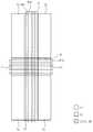
특히, 도 4에 도시된 바와 같이, 종래의 DRAM과 같은 반도체 장치에서 코어(Core) 영역에 배치되는 도전성 라인들(M6,M7,M8) 중 동일층에 형성되는 도전성 라인들(M7,M8)로 인해 레이아웃 면적이 증가할 수 있다.In particular, as shown in FIG. 4, conductive lines M7 and M8 formed on the same layer among conductive lines M6, M7, and M8 disposed in a core region in a semiconductor device such as a conventional DRAM. This can increase the layout area.
즉, 코어 영역에는 셀 어레이 영역들(40), 평면상 X축 방향으로 인접한 두 셀 어레이 영역(40) 사이에 각각 배치되는 서브 워드라인 드라이버 어레이 영역들(42), 평면상 Y축 방향으로 인접한 두 셀 어레이 영역(40) 사이에 각각 배치되는 비트라인 센스앰프 어레이 영역들(44), 서브 워드라인 드라이버 어레이 영역(42)과 비트라인 센스앰프 어레이 영역(44)이 교차하는 영역에 각각 배치되는 서브 홀 영역들(46) 등이 배치된다.That is, in the core region, the sub wordline
그리고, 비트라인 센스앰프 어레이 영역들(44)과 서브 홀 영역들(46)에는 도전성 라인들(M6)이 배치되고, 서브 워드라인 드라이버 어레이 영역들(42)과 서브 홀 영역들(46)에는 도전성 라인들(M7,M8)이 배치된다.Conductive lines M6 are disposed in the bit line sense
여기서, 도전성 라인들(M6)은 'L1'층에 형성되어 비트라인에 연결되는 세그먼트 입출력 라인들(SIO/SIOB)에 대응될 수 있으며, 도전성 라인들(M7)은 'L2'층에 형성되어 각 서브 워드라인 드라이버 어레이 영역(46)에 배치되는 서브 워드라인 드라이버(도시되지 않음)로 로우 어드레스를 전달하는 라인들 등에 대응될 수 있다. 또한, 도전성 라인들(M8)은 'L2'층에 형성되어 세그먼트 입출력 라인들(SIO/SIOB)과 전기적 연결을 이루는 로컬 입출력 라인들(LIO/LIOB)에 대응될 수 있다.The conductive lines M6 may be formed on the 'L1' layer and correspond to the segment input / output lines SIO / SIOB connected to the bit line, and the conductive lines M7 are formed on the 'L2' layer. The sub word line driver may correspond to lines that deliver a row address to a sub word line driver (not shown) disposed in each sub word line
이와 같이 종래의 DRAM과 같은 반도체 장치에서 서브 워드라인 드라이버 어레이 영역들(42)과 서브 홀 영역들(46)을 지나는 도전성 라인들(M7,M8)이 동일층에 형성되는 경우, 도전성 라인들(M7,M8)의 개수 증가에 따라 서브 워드라인 드라이버 어레이 영역들(42)과 서브 홀 영역들(46)의 면적이 증가하므로, 전체 메모리 칩 사이즈가 커질 수 있는 문제점이 있다.As described above, when the conductive lines M7 and M8 passing through the sub word line
또한, 메모리 칩 사이즈가 커짐에 따라 넷 다이(Net Die)의 개수가 작아져서 메모리 칩의 단가가 상승할 수 있는 문제점이 있다.In addition, as the memory chip size increases, the number of net dies decreases, thereby increasing the cost of the memory chip.
본 발명의 목적은 반도체 장치 내의 도전성 라인들을 효과적으로 배치하여 반도체 장치의 레이아웃 면적을 줄이고자 함에 있다.An object of the present invention is to reduce the layout area of a semiconductor device by effectively arranging conductive lines in the semiconductor device.
본 발명의 다른 목적은 서브 워드라인 드라이버 영역과 서브 홀 영역을 지나는 도전성 라인들이 차지하는 레이아웃 면적을 줄이고자 함에 있다.Another object of the present invention is to reduce the layout area occupied by conductive lines passing through the sub word line driver region and the sub hole region.
상기한 바와 같은 목적을 달성하기 위한 본 발명의 일면에 따른 반도체 장치는, 회로 블럭에 연결되며, 같은 신호를 인터페이스하는 복수의 제 1 도전성 라인이 동일층에 형성되는 제 1 라인 메쉬; 및 상기 제 1 도전성 라인이 형성된 층의 상부층과 하부층에 동일한 수의 제 2 도전성 라인들이 분할되어서 상기 제 1 도전성 라인들과 일대일 대응되어 인터페이스를 이루는 제 2 라인 메쉬;를 포함함을 특징으로 한다.In accordance with an aspect of the present invention, a semiconductor device includes: a first line mesh connected to a circuit block and having a plurality of first conductive lines formed on the same layer to interface the same signal; And a second line mesh in which the same number of second conductive lines are divided in an upper layer and a lower layer of the layer on which the first conductive line is formed to interface one-to-one with the first conductive lines to form an interface.
여기서, 상기 제 2 도전성 라인들은 상기 제 1 도전성 라인이 형성된 층의 상부층과 하부층에 오버랩되게 형성됨이 바람직하다.The second conductive lines may be formed to overlap the upper and lower layers of the layer on which the first conductive lines are formed.
그리고, 상기 제 1 라인 메쉬는 두 회로 블럭 사이에 형성되어 상기 두 회로 블럭 간의 신호를 인터페이스함이 바람직하다.The first line mesh may be formed between two circuit blocks to interface signals between the two circuit blocks.
또한, 상기 제 2 라인 메쉬는 상기 두 회로 블럭 사이에서 상기 제 1 라인 메쉬와 직교하게 형성됨이 바람직하다.In addition, the second line mesh is preferably formed orthogonal to the first line mesh between the two circuit blocks.
상기한 바와 같은 목적을 달성하기 위한 본 발명의 다른 일면에 따른 반도체 장치는, 회로 블럭에 연결되며, 같은 신호를 인터페이스하는 복수의 제 1 도전성 라인이 두층으로 분할 형성되는 제 1 라인 메쉬; 및 상기 제 1 라인 메쉬의 사이층에 상기 제 1 도전성 라인들과 동일한 수의 제 2 도전성 라인들이 일대일 대응되어 인터페이스를 이루는 제 2 라인 메쉬;를 포함함을 특징으로 한다.In accordance with another aspect of the present invention, a semiconductor device includes: a first line mesh connected to a circuit block and having a plurality of first conductive lines divided into two layers to interface the same signal; And a second line mesh interposed between the first line mesh and the same number of second conductive lines as the first conductive lines in a one-to-one correspondence to form an interface.
여기서, 상기 제 1 도전성 라인들은 상기 두층에 오버랩되게 분할 형성됨이 바람직하다.Here, the first conductive lines are preferably divided to overlap the two layers.
그리고, 상기 제 1 라인 메쉬는 두 회로 블럭 사이에 형성되어 상기 두 회로 블럭 간을 인터페이스함이 바람직하다.In addition, the first line mesh may be formed between two circuit blocks to interface between the two circuit blocks.
또한, 상기 제 2 라인 메쉬는 상기 두 회로 블럭 사이에서 상기 제 1 라인 메쉬와 직교하게 형성됨이 바람직하다.In addition, the second line mesh is preferably formed orthogonal to the first line mesh between the two circuit blocks.
상기한 바와 같은 목적을 달성하기 위한 본 발명의 또 다른 일면에 따른 반도체 장치는, 비트라인 센스앰프 어레이 영역에 연결되는 복수의 제 1 도전성 라인이 동일층에 형성되는 제 1 라인 메쉬; 및 서브 워드라인 드라이버 어레이 영역에 배치되며, 복수의 제 2 도전성 라인과, 상기 제 1 도전성 라이들과 인터페이스를 이루는 복수의 제 3 도전성 라인이 상기 제 1 도전성 라인들이 형성되는 층의 상부층과 하부층에 각각 형성되는 제 2 라인 메쉬;를 포함함을 특징으로 한다.According to still another aspect of the present invention, there is provided a semiconductor device including: a first line mesh having a plurality of first conductive lines connected to a bit line sense amplifier array region formed on the same layer; And a plurality of second conductive lines and a plurality of third conductive lines interfaced with the first conductive liner in the upper and lower layers of the layer in which the first conductive lines are formed. And a second line mesh to be formed.
여기서, 상기 도전성 라인들과 상기 제 2 및 제 3 도전성 라인들은 상기 제 1 도전성 라인들이 형성되는 층의 상부층과 하부층에 오버랩되게 각각 형성이 바람직하다.Here, the conductive lines and the second and third conductive lines are preferably formed so as to overlap the upper layer and the lower layer of the layer where the first conductive lines are formed.
그리고, 상기 제 1 도전성 라인들은 상기 비트라인 센스앰프 어레이에 데이터를 인터페이스하는 세그먼트 입출력 라인들에 대응되고, 상기 제 2 도전성 라인 들은 상기 서브 워드라인 드라이버 어레이를 선택하는 신호를 전달하는 라인에 대응되며, 상기 제 3 도전성 라인들은 상기 세그먼트 입출력 라인들과 인터페이스를 이루는 로컬 입출력 라인들에 대응됨이 바람직하다.The first conductive lines correspond to segment input / output lines for interfacing data to the bit line sense amplifier array, and the second conductive lines correspond to a line for transmitting a signal for selecting the sub word line driver array. The third conductive lines may correspond to local I / O lines that interface with the segment I / O lines.
또한, 상기 제 1 도전성 라인들은 상기 비트라인 센스앰프 어레이 영역과 상기 서브 워드라인 드라이버 어레이 영역이 교차하는 서브 홀 영역에서 상기 제 2 및 제 3 도전성 라인들과 교차됨이 바람직하다.The first conductive lines may cross the second and third conductive lines in a sub hole area where the bit line sense amplifier array area and the sub word line driver array area cross each other.
이하, 첨부한 도면을 참조하여 본 발명의 바람직한 실시 예를 상세하게 설명하기로 한다.Hereinafter, exemplary embodiments of the present invention will be described in detail with reference to the accompanying drawings.
본 발명의 반도체 장치는 라인 메쉬를 이루는 도전성 라인들 중 같은 신호를 인터페이스하는 도전성 라인들이 두 층에 분할 형성된 구조를 갖는다.The semiconductor device of the present invention has a structure in which conductive lines for interfacing the same signal among the conductive lines constituting the line mesh are divided in two layers.
구체적으로, 본 발명의 반도체 장치는 실시 예로서, 도 5 내지 도 7과 같은 레이아웃 구조를 가질 수 있다.Specifically, the semiconductor device of the present invention may have a layout structure as shown in FIGS. 5 to 7 as an embodiment.
도 5 내지 도 7에서, 도면 부호 'L1~L3'은 서로 다른 층을 의미하며, 바람직하게는 'L2', 'L1', 및 'L3' 순으로 층을 이룬다.5 to 7, reference numerals 'L1 to L3' mean different layers, and are preferably layered in order of 'L2', 'L1', and 'L3'.
또한, 도면 부호 'L1CL2'은 'L1'층에 형성되는 도전성 라인과 'L2'층에 형성되는 도전성 라인 간을 전기적으로 연결하는 콘택을 의미하고, 도면 부호 'L2CL3'는 'L2'층에 형성되는 도전성 라인과 'L3'층에 형성되는 도전성 라인 간을 전기적으로 연결하는 콘택을 의미한다.In addition, the reference numeral 'L1CL2' refers to a contact electrically connecting the conductive lines formed on the 'L1' layer and the conductive lines formed on the 'L2' layer, and the reference numeral 'L2CL3' is formed on the 'L2' layer. The contact means for electrically connecting between the conductive line is formed and the conductive line formed in the 'L3' layer.
아울러, 도면 부호 'L1L3 OVERLAP'은 'L1'층에 형성되는 도전성 라인과 'L3'층에 형성되는 도전성 라인이 오버랩된 것을 의미하고, 도면 부호 'L2L3 OVERLAP' 은 'L2'층에 형성되는 도전성 라인과 'L3'층에 형성되는 도전성 라인이 오버랩된 것을 의미한다.In addition, the reference numeral 'L1L3 OVERLAP' means that the conductive line formed in the 'L1' layer and the conductive line formed in the 'L3' layer overlap, and the reference numeral 'L2L3 OVERLAP' refers to the conductive formed in the 'L2' layer. It means that the line and the conductive line formed in the 'L3' layer overlap.
우선, 본 발명의 반도체 장치는 제 1 실시 예로, 도 5에 도시된 바와 같이, 다수의 유닛 셀(50a,50b)과 글로벌 입출력 영역(58)을 포함하는 구조를 갖는다. 여기서, 유닛 셀(50a)은 두 회로 블럭(52a,54a)과, 두 회로 블럭(52a,54a) 사이에 배치되는 라인 메쉬(56a)를 한정하는 영역을 의미하며, 유닛 셀(50b)은 두 회로 블럭(52b,54b)과, 두 회로 블럭(52b,54b) 사이에 배치되는 라인 메쉬(56b)를 한정하는 영역을 의미한다.First, the semiconductor device of the present invention has a structure including a plurality of
그리고, 라인 메쉬(56a)는 회로 블럭(52a)과 회로 블럭(54a) 간의 신호를 인터페이스하는 도전성 라인들(M9a)과, 도전성 라인들(M9a)에 교차하는 도전성 라인들(M10a)을 포함하며, 라인 메쉬(56b)는 회로 블럭(52b)과 회로 블럭(54b) 간의 신호를 인터페이스하는 도전성 라인들(M9b)과, 도전성 라인들(M9b)에 교차하는 도전성 라인들(M10b)을 포함한다.The
여기서, 도전성 라인들(M9a,M9b)은 'L1'층에 형성되고, 도전성 라인들(M10a,M10b)은 'L2'층와 'L3'층에 각각 분할 형성된다. 그리고, 'L2'층에 형성되는 절반의 도전성 라인들(M10a,M10b)과 'L3'층에 형성되는 나머지 절반의 도전성 라인들(M10a,M10b)은 서로 오버랩되게 배치될 수 있다.Here, the conductive lines M9a and M9b are formed in the 'L1' layer, and the conductive lines M10a and M10b are divided into the 'L2' layer and the 'L3' layer, respectively. The half of the conductive lines M10a and M10b formed in the 'L2' layer and the other half of the conductive lines M10a and M10b formed in the 'L3' layer may overlap each other.
예를 들어, 도전성 라인들(M9a)의 상부층에 도전성 라인들(M10a)의 절반이 교차되게 형성되고, 그 상부층에 나머지 절반의 도전성 라인들(M10a)이 절반의 도전성 라인들(M10a)과 오버랩되게 형성될 수 있다. 그리고, 각 도전성 라인 들(M10a,M10b)은 도면에 도시되지 않은 다른 회로 블럭과 전기적으로 연결될 수 있다.For example, half of the conductive lines M10a are formed to cross the upper layers of the conductive lines M9a, and the other half of the conductive lines M10a overlap the half of the conductive lines M10a on the upper layer. Can be formed. Each of the conductive lines M10a and M10b may be electrically connected to another circuit block not shown in the drawing.
글로벌 입출력 영역(58)에는 도전성 라인들(M10a,M10b)과 인터페이스를 이루는 도전성 라인들(M11)과, 글로벌 입출력 영역(58)을 지나는 도전성 라인들(M12)이 교차하도록 배치된다.In the global input /
여기서, 도전성 라인들(M11)은 'L1'층와 'L3'층에 각각 분할 형성된다. 그리고, 'L1'층에 형성되는 절반의 도전성 라인들(M11)은 콘택(L1CL3)을 통해 'L3'층에 형성되는 도전성 라인들(M10a,M10b)과 일대일 대응되게 전기적으로 연결되고, 'L3'층에 형성되는 나머지 절반의 도전성 라인들(M11)은 콘택(L2CL3)을 통해 'L2'층에 형성되는 도전성 라인들(M10a,M10b)과 일대일 대응되게 전기적으로 연결된다.In this case, the conductive lines M11 are separately formed on the 'L1' layer and the 'L3' layer. The half conductive lines M11 formed in the 'L1' layer are electrically connected to the conductive lines M10a and M10b formed in the 'L3' layer through the contact L1CL3 in a one-to-one correspondence. The other half of the conductive lines M11 formed in the 'layer' are electrically connected in a one-to-one correspondence with the conductive lines M10a and M10b formed in the 'L2' layer through the contact L2CL3.
또한, 도전성 라인들(M12)은 'L2'층에 형성되며, 도전성 라인들(M12)의 절반은 콘택(L1CL2)을 통해 'L1'층에 형성되는 도전성 라인들(M11)과 일대일 대응되게 전기적으로 연결되고, 도전성 라인들(M12)의 나머지 절반은 콘택(L2CL3)을 통해 'L3'층에 형성되는 도전성 라인들(M12)과 일대일 대응되게 전기적으로 연결된다. 그리고, 도전성 라인들(M12)은 일 예로, 최소한 둘 이상의 회로 블럭에 공통으로 연결되어 상기 회로 블럭들 중 어느 하나에서 전달된 신호를 외부로 전달하는 글로벌 라인이 될 수 있다.In addition, the conductive lines M12 are formed in the 'L2' layer, and half of the conductive lines M12 are electrically connected to the conductive lines M11 formed in the 'L1' layer through the contact L1CL2. The other half of the conductive lines M12 is electrically connected to the conductive lines M12 formed in the 'L3' layer through the contact L2CL3 in a one-to-one correspondence. For example, the conductive lines M12 may be connected to at least two circuit blocks in common, and may be global lines that transmit signals transmitted from any one of the circuit blocks to the outside.
이와 같이, 본 발명의 제 1 실시 예에 따른 반도체 장치는 도전성 라인들(M10a,M10b)이 반씩 서로 다른 층에 오버랩되게 배치되고, 도전성 라인들(M10a,M10b)과 전기적으로 연결되는 도전성 라인들(M11)도 마찬가지로 반씩 서로 다른 층에 오버랩되게 배치된 레이아웃 구조를 갖는다.As described above, in the semiconductor device according to the first embodiment of the present invention, conductive lines M10a and M10b are disposed to overlap each other in half, and conductive lines electrically connected to the conductive lines M10a and M10b. Similarly, M11 has a layout structure arranged so as to overlap each other in half.
즉, 두 회로 블럭(예컨대, 52a,54a) 사이를 지나는 도전성 라인들(M10a,M10b)이 반씩 서로 다른 층에 오버랩되게 배치됨으로써, 라인 메쉬(56a)의 레이아웃 면적이 줄어들 수 있으며, 그에 따라, 각 유닛 셀(50a,50b)의 면적이 줄어들 수 있는 효과가 있다.That is, the conductive lines M10a and M10b passing between the two circuit blocks (eg, 52a and 54a) are disposed to overlap each other in half, so that the layout area of the
본 발명의 반도체 장치는 제 2 실시 예로서, 도 6의 레이아웃 구조가 개시될 수 있다.As a second embodiment of the present invention, the layout structure of FIG. 6 may be disclosed.
도 6을 참조하면, 본 발명의 제 2 실시 예에 따른 반도체 장치는 도 5와 마찬가지로 다수의 유닛 셀(60a,60b)과 글로벌 입출력 영역(68)을 포함하는 구조를 갖는다.Referring to FIG. 6, the semiconductor device according to the second exemplary embodiment of the present inventive concept has a structure including a plurality of
유닛 셀(60a)의 두 회로 블럭(62a,64a) 사이에 배치되는 라인 메쉬(66a)는 회로 블럭(62a)과 회로 블럭(64a) 간의 신호를 인터페이스하는 도전성 라인들(M13a)과, 도전성 라인들(M13a)과 인터페이스를 이루는 도전성 라인들(M14a)을 포함한다.The
또한, 유닛 셀(60b)의 두 회로 블럭(62b,64b) 사이에 배치되는 라인 메쉬(66b)는 회로 블럭(62b)과 회로 블럭(64b) 간의 신호를 인터페이스하는 도전성 라인들(M13b)과, 도전성 라인들(M13b)과 인터페이스를 이루는 도전성 라인들(M14b)을 포함한다.In addition, the
여기서, 도전성 라인들(M13a,M13b)은 'L1'층와 'L3'층에 각각 분할 형성되고, 도전성 라인들(M14a,M14b)은 'L2'층에 형성된다. 그리고, 'L1'층에 형성되는 절반의 도전성 라인들(M13a,M13b)과 'L3'층에 형성되는 나머지 절반의 도전성 라인들(M13a,M13b)은 서로 오버랩되게 배치될 수 있다.Here, the conductive lines M13a and M13b are respectively formed in the 'L1' layer and the 'L3' layer, and the conductive lines M14a and M14b are formed in the 'L2' layer. The half conductive lines M13a and M13b formed in the 'L1' layer and the other half conductive lines M13a and M13b formed in the 'L3' layer may overlap each other.
이때, 'L1'층에 형성되는 절반의 도전성 라인들(M13a,M13b)은 콘택(L1CL2)을 통해 도전성 라인들(M14a,M14b)의 절반과 일대일 대응되게 각각 전기적으로 연결되고, 'L3'층에 형성되는 나머지 절반의 도전성 라인들(M13a,M13b)은 콘택(L2CL3)을 통해 도전성 라인들(M14a,M14b)의 나머지 절반과 일대일 대응되게 각각 전기적으로 연결된다.In this case, half of the conductive lines M13a and M13b formed in the 'L1' layer are electrically connected to each other in a one-to-one correspondence with the half of the conductive lines M14a and M14b through the contact L1CL2, and the 'L3' layer. The other half of the conductive lines M13a and M13b formed at are electrically connected to each other in a one-to-one correspondence with the other half of the conductive lines M14a and M14b through the contact L2CL3.
글로벌 입출력 영역(68)에는 도전성 라인들(M14a,M14b)과 인터페이스를 이루는 도전성 라인들(M15)과, 글로벌 입출력 영역(68)을 지나는 도전성 라인들(M12)이 교차하도록 배치된다. 여기서, 도전성 라인들(M15)은 콘택(L1CL2)을 통해 도전성 라인들(M14a,M14b)과 일대일 대응되게 전기적으로 연결된다.In the global input /
이와 같이, 본 발명의 제 2 실시 예에 따른 반도체 장치는 회로 블럭(예컨대, 62a)과 회로 블럭(예컨대, 64a) 간의 신호를 인터페이스하는 도전성 라인들(M13a)이 서로 다른 층에 분할 형성된 레이아웃 구조를 갖는다.As described above, the semiconductor device according to the second embodiment of the present invention has a layout structure in which conductive lines M13a for interfacing a signal between a circuit block (eg, 62a) and a circuit block (eg, 64a) are formed in different layers. Has
따라서, 두 회로 블럭(62a,64a) 사이의 라인 메쉬(66a)에서 도전성 라인들(M14a)이 형성되는 층을 제외한 다른 층에서의 여유 공간이 늘어날 수 있으므로, 라인 영역(66a)에 두 회로 블럭(62a,64a) 간의 신호를 인터페이스하는 도전성 라인들 또는 두 회로 블럭(62a,64a) 사이 영역을 지나는 다른 도전성 라인들이 더 많이 배치될 수 있는 효과가 있다.Therefore, since the free space in the other layer except for the layer in which the conductive lines M14a are formed in the
본 발명의 반도체 장치는 제 3 실시 예로서, 도 7과 같은 메모리 장치의 코 어 영역의 레이아웃 구조를 가질 수 있다.In a third embodiment of the present invention, the semiconductor device may have a layout structure of a core region of the memory device as shown in FIG. 7.
도 7을 참조하면, 본 발명의 제 3 실시 예에 따른 반도체 장치의 코어 영역에는 셀 어레이 영역들(70), 평면상 X축 방향으로 인접한 두 셀 어레이 영역(70) 사이에 각각 배치되는 서브 워드라인 드라이버 어레이 영역들(72), 평면상 Y축 방향으로 인접한 두 셀 어레이 영역(70) 사이에 각각 배치되는 비트라인 센스앰프 어레이 영역들(74), 서브 워드라인 드라이버 어레이 영역(72)과 비트라인 센스앰프 어레이 영역(74)이 교차하는 영역에 각각 배치되는 서브 홀 영역들(76) 등이 배치된다.Referring to FIG. 7, in the core region of the semiconductor device according to the third exemplary embodiment of the present invention, a sub word is disposed between the
여기서, 도면에 도시하지 않았지만, 각 셀 어레이 영역(70)에는 다수의 메모리 셀이 배치될 수 있고, 각 서브 워드라인 드라이버 어레이 영역(72)에는 상기 메모리 셀에 연결된 서브 워드라인을 구동하는 다수의 서브 워드라인 드라이버 등이 배치될 수 있다.Although not shown in the drawings, a plurality of memory cells may be disposed in each
또한, 각 비트라인 센스앰프 어레이 영역(74)에는 상기 메모리 셀에 연결된 비트라인의 전위차를 감지 증폭하는 다수의 비트라인 센스앰프 등이 배치될 수 있으며, 각 서브 홀 영역(76)에는 상기 각 비트라인 센스앰프를 구동하는 센스앰프 드라이버 및 서브 워드라인을 선택하는 로우 어드레스를 구동하는 드라이버 등이 배치될 수 있다.In addition, a plurality of bit line sense amplifiers may be disposed in each bit line sense
비트라인 센스앰프 어레이 영역들(64)과 서브 홀 영역들(76)을 가로질러 도전성 라인들(M16)이 배치되고, 서브 워드라인 드라이버 어레이 영역들(72)과 서브 홀 영역들(66)을 가로질러 도전성 라인들(M17,M18)이 배치된다.Conductive lines M16 are disposed across the bit line sense amplifier array regions 64 and the
여기서, 도전성 라인들(M16)은 세그먼트 입출력 라인들(SIO/SIOB)에 대응될 수 있으며, 도전성 라인들(M17)은 서브 워드라인 드라이버(도시되지 않음)로 로우 어드레스를 전달하는 라인들 등에 대응될 수 있다. 또한, 도전성 라인들(M18)은 세그먼트 입출력 라인들(SIO/SIOB)과 인터페이스를 이루는 로컬 입출력 라인들(LIO/LIOB)에 대응될 수 있다.The conductive lines M16 may correspond to the segment input / output lines SIO / SIOB, and the conductive lines M17 may correspond to lines that deliver row addresses to a sub word line driver (not shown). Can be. In addition, the conductive lines M18 may correspond to local input / output lines LIO / LIOB that interface with the segment input / output lines SIO / SIOB.
아울러, 도전성 라인들(M16)은 'L1'층에 형성되고, 도전성 라인들(M17)은 'L2'층에 형성되며, 도전성 라인들(M18)은 'L3'층에 형성된다. 이때, 도전성 라인들(M16)은 서브 홀 영역(76)에서 도전성 라인들(M17,M18)과 각각 교차하며, 도전성 라인들(M17)과 도전성 라인들(M18)은 서로 다른 층에서 오버랩되거나 평면상 서로 인접하게 배치될 수 있다.In addition, the conductive lines M16 are formed in the 'L1' layer, the conductive lines M17 are formed in the 'L2' layer, and the conductive lines M18 are formed in the 'L3' layer. In this case, the conductive lines M16 cross the conductive lines M17 and M18 in the
이와 같이, 본 발명의 제 3 실시 예에 따른 반도체 장치는 서브 워드라인 드라이버 어레이 영역들(72)과 서브 홀 영역들(66)을 가로질러 배치되는 도전성 라인들(M17,M18)이 서로 다른 층에 오버랩되게(또는 서로 인접하게) 형성된 레이아웃 구조를 갖는다.As described above, in the semiconductor device according to the third exemplary embodiment, the conductive lines M17 and M18 disposed across the sub word line
따라서, 도전성 라인들(M17,M18)이 지나는 서브 워드라인 드라이버 어레이 영역들(72)과 서브 홀 영역들(66)의 레이아웃 면적이 줄어들 수 있으므로, 전체 메모리 칩 사이즈가 줄어들 수 있는 효과가 있다.Therefore, the layout area of the sub word line
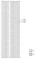
이상에서 살펴본 바와 같이, 본 발명의 반도체 메모리 장치는 한 층에 배치되는 라인들이 최소한 둘 이상의 층에 오버랩되게 분산 배치된 구조를 갖는다. 이때, 서로 다른 층의 라인들이 오버랩되면, 라인들 간의 커플링(coupling)이 발생할 수 있다.As described above, the semiconductor memory device of the present invention has a structure in which lines disposed in one layer are distributed and overlapped with at least two layers. At this time, when lines of different layers overlap, coupling between lines may occur.
이 경우, 본 발명은 도 8에 도시된 바와 같이, 소정 층(예컨대, 'L1' 층)에 형성되는 라인(M19)과 다른 층(예컨대, 'L3' 층)에 형성되는 라인(M20)을 평면상 인접하게 배치함으로써, 라인들 간의 커플링을 효과적으로 개선할 수 있다.In this case, as shown in FIG. 8, the present invention provides a line M20 formed in a layer M19 formed on a predetermined layer (eg, an 'L1' layer) and a layer different from the line M19 formed (eg, an 'L3' layer). By arranging adjacent in plane, it is possible to effectively improve the coupling between the lines.
본 발명은 한 층에 배치되는 라인들을 두 층에 분할 배치함으로써, 라인들이 차지하는 레이아웃 면적을 줄일 수 있으며, 그에 따라, 반도체 장치의 사이즈가 작아져서 넷 다이의 개수가 증가하고 단가도 하강할 수 있는 효과가 있다.According to the present invention, by dividing lines arranged in one layer into two layers, the layout area occupied by the lines can be reduced. Accordingly, the size of the semiconductor device can be reduced, so that the number of net dies can be increased and the cost can be lowered. It works.
또한, 본 발명은 서브 워드라인 드라이버 영역과 서브 홀 영역을 지나는 라인들을 서로 다른 층에 배치함으로써, 상기 서브 워드라인 드라이버 영역과 서브 홀 영역의 레이아웃 면적이 줄어들 수 있는 효과가 있다.In addition, the present invention has an effect that the layout area of the sub word line driver region and the sub hole region can be reduced by arranging lines passing through the sub word line driver region and the sub hole region in different layers.
본 발명을 특정 실시 예에 관련하여 도시하고 설명하였지만, 본 발명이 그에 한정되는 것은 아니며, 이하의 특허청구범위에 의해 마련되는 본 발명의 정신이나 분야를 이탈하지 않는 한도 내에서 본 발명이 다양하게 개조 및 변형될 수 있다는 것을 당업자는 용이하게 알 수 있다.While the invention has been shown and described with reference to specific embodiments, the invention is not limited thereto, and the invention is not limited to the scope of the invention as defined by the following claims. Those skilled in the art will readily appreciate that modifications and variations can be made.
Claims (21)
Translated fromKoreanPriority Applications (1)
| Application Number | Priority Date | Filing Date | Title |
|---|---|---|---|
| KR1020070042244AKR100833596B1 (en) | 2007-04-30 | 2007-04-30 | Semiconductor device and its layout method |
Applications Claiming Priority (1)
| Application Number | Priority Date | Filing Date | Title |
|---|---|---|---|
| KR1020070042244AKR100833596B1 (en) | 2007-04-30 | 2007-04-30 | Semiconductor device and its layout method |
Publications (1)
| Publication Number | Publication Date |
|---|---|
| KR100833596B1true KR100833596B1 (en) | 2008-05-30 |
Family
ID=39665633
Family Applications (1)
| Application Number | Title | Priority Date | Filing Date |
|---|---|---|---|
| KR1020070042244AExpired - Fee RelatedKR100833596B1 (en) | 2007-04-30 | 2007-04-30 | Semiconductor device and its layout method |
Country Status (1)
| Country | Link |
|---|---|
| KR (1) | KR100833596B1 (en) |
Citations (2)
| Publication number | Priority date | Publication date | Assignee | Title |
|---|---|---|---|---|
| KR100541818B1 (en) | 2003-12-18 | 2006-01-10 | 삼성전자주식회사 | Line Arrangement Structure of Semiconductor Memory Device |
| KR20060023866A (en)* | 2004-09-10 | 2006-03-15 | 삼성전자주식회사 | Semiconductor memory device and placement method thereof |
- 2007
- 2007-04-30KRKR1020070042244Apatent/KR100833596B1/ennot_activeExpired - Fee Related
Patent Citations (2)
| Publication number | Priority date | Publication date | Assignee | Title |
|---|---|---|---|---|
| KR100541818B1 (en) | 2003-12-18 | 2006-01-10 | 삼성전자주식회사 | Line Arrangement Structure of Semiconductor Memory Device |
| KR20060023866A (en)* | 2004-09-10 | 2006-03-15 | 삼성전자주식회사 | Semiconductor memory device and placement method thereof |
Similar Documents
| Publication | Publication Date | Title |
|---|---|---|
| US7679985B2 (en) | Semiconductor memory device and arrangement method thereof | |
| JP2008182058A (en) | Semiconductor device and semiconductor device forming method | |
| US8823173B2 (en) | Semiconductor device having plurality of wiring layers and designing method thereof | |
| US8237200B2 (en) | Methods of arranging L-shaped cell blocks in semiconductor devices | |
| US20100328985A1 (en) | Semiconductor device having plural circuit blocks laid out in a matrix form | |
| CN108886020A (en) | semiconductor integrated circuit device | |
| US20120256243A1 (en) | Semiconductor device for reducing interconnect pitch | |
| KR100833596B1 (en) | Semiconductor device and its layout method | |
| US7242602B2 (en) | Semiconductor memory devices having conductive line in twisted areas of twisted bit line pairs | |
| US9379053B2 (en) | Semiconductor device having signal line and power supply line intersecting with each other | |
| US7652904B2 (en) | Semiconductor memory device having plural memory cell arrays | |
| US20030140323A1 (en) | Method of designing semiconductor integrated circuit device and semiconductor integrated circuit device manufactured using the same | |
| CN110176265B (en) | Multilayer memory and method of making the same | |
| JP2009026868A (en) | Semiconductor integrated circuit and design method thereof | |
| US7235855B2 (en) | Semiconductor device having a layout configuration for minimizing crosstalk | |
| JP7385113B2 (en) | semiconductor memory device | |
| JP5571873B2 (en) | Semiconductor device and layout method thereof | |
| US6529406B1 (en) | Semiconductor device with power supply wirings and expanded wirable regions for users | |
| KR20090088262A (en) | Wiring arrangement method of semiconductor memory device | |
| US6596626B2 (en) | Method for arranging wiring line including power reinforcing line and semiconductor device having power reinforcing line | |
| JP5385575B2 (en) | Semiconductor memory device | |
| JP2005332903A (en) | Semiconductor device | |
| US20050248042A1 (en) | Semiconductor memory device | |
| US6833624B2 (en) | System and method for row decode in a multiport memory | |
| JP2003324160A (en) | Semiconductor memory device |
Legal Events
| Date | Code | Title | Description |
|---|---|---|---|
| A201 | Request for examination | ||
| PA0109 | Patent application | St.27 status event code:A-0-1-A10-A12-nap-PA0109 | |
| PA0201 | Request for examination | St.27 status event code:A-1-2-D10-D11-exm-PA0201 | |
| E701 | Decision to grant or registration of patent right | ||
| PE0701 | Decision of registration | St.27 status event code:A-1-2-D10-D22-exm-PE0701 | |
| GRNT | Written decision to grant | ||
| PR0701 | Registration of establishment | St.27 status event code:A-2-4-F10-F11-exm-PR0701 | |
| PR1002 | Payment of registration fee | St.27 status event code:A-2-2-U10-U11-oth-PR1002 Fee payment year number:1 | |
| PG1601 | Publication of registration | St.27 status event code:A-4-4-Q10-Q13-nap-PG1601 | |
| FPAY | Annual fee payment | Payment date:20110429 Year of fee payment:4 | |
| PR1001 | Payment of annual fee | St.27 status event code:A-4-4-U10-U11-oth-PR1001 Fee payment year number:4 | |
| PN2301 | Change of applicant | St.27 status event code:A-5-5-R10-R13-asn-PN2301 St.27 status event code:A-5-5-R10-R11-asn-PN2301 | |
| LAPS | Lapse due to unpaid annual fee | ||
| PC1903 | Unpaid annual fee | St.27 status event code:A-4-4-U10-U13-oth-PC1903 Not in force date:20120524 Payment event data comment text:Termination Category : DEFAULT_OF_REGISTRATION_FEE | |
| PN2301 | Change of applicant | St.27 status event code:A-5-5-R10-R13-asn-PN2301 St.27 status event code:A-5-5-R10-R11-asn-PN2301 | |
| PC1903 | Unpaid annual fee | St.27 status event code:N-4-6-H10-H13-oth-PC1903 Ip right cessation event data comment text:Termination Category : DEFAULT_OF_REGISTRATION_FEE Not in force date:20120524 | |
| PN2301 | Change of applicant | St.27 status event code:A-5-5-R10-R13-asn-PN2301 St.27 status event code:A-5-5-R10-R11-asn-PN2301 | |
| P22-X000 | Classification modified | St.27 status event code:A-4-4-P10-P22-nap-X000 | |
| P22-X000 | Classification modified | St.27 status event code:A-4-4-P10-P22-nap-X000 |