KR100833513B1 - Impedance Matching Device and Method in Sensor Node - Google Patents
Impedance Matching Device and Method in Sensor NodeDownload PDFInfo
- Publication number
- KR100833513B1 KR100833513B1KR1020060125052AKR20060125052AKR100833513B1KR 100833513 B1KR100833513 B1KR 100833513B1KR 1020060125052 AKR1020060125052 AKR 1020060125052AKR 20060125052 AKR20060125052 AKR 20060125052AKR 100833513 B1KR100833513 B1KR 100833513B1
- Authority
- KR
- South Korea
- Prior art keywords
- impedance matching
- impedance
- sensor node
- output signal
- intensity
- Prior art date
- Legal status (The legal status is an assumption and is not a legal conclusion. Google has not performed a legal analysis and makes no representation as to the accuracy of the status listed.)
- Expired - Fee Related
Links
Images


Classifications
- H—ELECTRICITY
- H01—ELECTRIC ELEMENTS
- H01P—WAVEGUIDES; RESONATORS, LINES, OR OTHER DEVICES OF THE WAVEGUIDE TYPE
- H01P1/00—Auxiliary devices
- H01P1/10—Auxiliary devices for switching or interrupting
- H—ELECTRICITY
- H03—ELECTRONIC CIRCUITRY
- H03H—IMPEDANCE NETWORKS, e.g. RESONANT CIRCUITS; RESONATORS
- H03H7/00—Multiple-port networks comprising only passive electrical elements as network components
- H03H7/38—Impedance-matching networks
- H03H7/40—Automatic matching of load impedance to source impedance
- H—ELECTRICITY
- H01—ELECTRIC ELEMENTS
- H01P—WAVEGUIDES; RESONATORS, LINES, OR OTHER DEVICES OF THE WAVEGUIDE TYPE
- H01P5/00—Coupling devices of the waveguide type
- H—ELECTRICITY
- H01—ELECTRIC ELEMENTS
- H01Q—ANTENNAS, i.e. RADIO AERIALS
- H01Q1/00—Details of, or arrangements associated with, antennas
- H—ELECTRICITY
- H04—ELECTRIC COMMUNICATION TECHNIQUE
- H04B—TRANSMISSION
- H04B1/00—Details of transmission systems, not covered by a single one of groups H04B3/00 - H04B13/00; Details of transmission systems not characterised by the medium used for transmission
- H04B1/38—Transceivers, i.e. devices in which transmitter and receiver form a structural unit and in which at least one part is used for functions of transmitting and receiving
- H04B1/40—Circuits
Landscapes
- Engineering & Computer Science (AREA)
- Computer Networks & Wireless Communication (AREA)
- Signal Processing (AREA)
- Transmitters (AREA)
Abstract
Translated fromKoreanDescription
Translated fromKorean도 1은 일반적인 WSN(Wireless Sensor Network)용 센서 노드(Sensor Node)의 구성을 나타내는 도면이다.1 is a diagram illustrating a configuration of a sensor node for a general wireless sensor network (WSN).
도 2는 본 발명의 바람직한 일 실시예에 의한 센서 노드에 있어서의 임피던스 정합장치의 구성을 나타내는 도면이다.2 is a view showing the configuration of the impedance matching device in the sensor node according to an embodiment of the present invention.
도 3은 본 발명의 바람직한 일 실시예에 의한 센서 노드에 있어서의 임피던스 정합방법의 흐름을 보여주는 도면이다.3 is a view showing the flow of the impedance matching method in the sensor node according to an embodiment of the present invention.
본 발명은 센서 노드에 있어서의 임피던스 정합장치 및 그 방법에 관한 것으로, 보다 상세하게는 WSN(Wireless Sensor Network)에 사용되는 센서 노드의 RF(Radio Frequency)전송 효율을 높이기 위한 임피던스 정합장치 및 그 방법에 관한 것이다.The present invention relates to an impedance matching device in a sensor node and a method thereof, and more particularly, to an impedance matching device and a method for increasing RF (Radio Frequency) transmission efficiency of a sensor node used in a WSN (Wireless Sensor Network). It is about.
최근 무선 네트워크 기술이 빠르게 향상됨으로 인하여 이동 무선 컴퓨팅에 대한 응용 범위와 빈도가 급격히 증가하고 있다.Recently, due to the rapid improvement of wireless network technology, the application range and frequency of mobile wireless computing are rapidly increasing.
이동 무선 컴퓨팅 네트워크에서는 각 노드들끼리 데이터를 전달할 수 있어야 한다. 또한, 배터리 유지에 따른 데이터 전송 반경이 제한되며, 낮은 대역폭과 높은 에러율을 가진다.In a mobile wireless computing network, each node must be able to carry data. In addition, the data transmission radius due to battery maintenance is limited, and has a low bandwidth and a high error rate.
이러한 단점에도 불구하고, 이동 무선 컴퓨팅 네트워크는 기반 구조가 없는 전쟁터 및 전시장 등과 같은 장소에서 효과적으로 사용될 수 있다.Despite these drawbacks, mobile wireless computing networks can be effectively used in places such as battlefields and exhibition halls without infrastructure.
재난 구조, 산불 감시, 전시 작전 등을 위하여 사용되는 센서 노드는 현장에 사용될 때 내부 전원을 교체하는 비용이 높거나 불가능한 경우가 많다. 이러한 분야에 사용되는 센서 노드는 센서 노드가 현장에서 사용되기 전에 장착된 내부 전원이 모두 소모되는 기간 동안만 사용이 가능한 경우가 많다.Sensor nodes used for disaster relief, forest fire monitoring and wartime operations are often expensive or impossible to replace internal power when used in the field. Sensor nodes used in these applications are often available only during periods when the installed internal power is exhausted before the sensor node is used in the field.
따라서 센서 노드의 한정된 내부 전원을 효율적으로 이용하여 안테나를 통해 필요한 전파를 방사하기 위하여 전송부와 안테나 사이의 임피던스 정합이 이루어져야 한다.Therefore, the impedance matching between the transmitter and the antenna must be made in order to radiate necessary radio waves through the antenna by efficiently using the limited internal power of the sensor node.
일반적으로 WSN용 센서 노드의 전송부는 주로 모뎀, RF(Radio Frequency) 회로, 임피던스 정합 회로가 포함된 하나의 칩으로 이루어져 있으며 고정된 임피던스 값을 나타낸다. 따라서 센서 노드 내의 안테나는 칩의 고정된 임피던스 값에 맞게 설계되어 장착된다.In general, the transmitter of the WSN sensor node mainly consists of one chip including a modem, a radio frequency (RF) circuit, and an impedance matching circuit, and exhibits a fixed impedance value. Therefore, the antenna within the sensor node is designed and mounted to the fixed impedance value of the chip.
그러나 센서 노드가 실제 현장에 적용되어 사용될 때에는, 안테나의 각도, 주변 사물의 전기적 특성 등에 의해 영향을 받아 안테나의 공진 주파수가 이동하는 현상이 발생된다.However, when the sensor node is applied and used in the actual field, the resonance frequency of the antenna is shifted due to the angle of the antenna and the electrical characteristics of the surrounding objects.
즉, 안테나의 임피던스 값이 달라지는 현상이 발생하여, 전송부와 안테나 사 이의 임피던스 정합 불일치에 따라 전송 효율이 저하된다.That is, the phenomenon that the impedance value of the antenna is changed occurs, the transmission efficiency is reduced due to the impedance mismatch between the transmitter and the antenna.
하지만, WSN에서 사용되는 센서 노드는 애드 혹(Ad-hoc)통신 방식을 이용하여 대등한 장비들 간의 접속을 통하여 통신 회선이 확보되므로, 중앙에서 통신 감도를 조절하는 기지국 등의 장치가 따로 구비되어 있지 않다.However, the sensor node used in the WSN is secured a communication line through the connection between the equivalent equipment using the ad-hoc communication method, so that a device such as a base station for controlling the communication sensitivity is provided separately. Not.
센서 노드의 사용 환경에서 따라 임피던스 값이 변화하여 센서 노드의 통신 성능이 저하되는 취약점을 보완할 필요가 있다.It is necessary to compensate for the vulnerability that the communication performance of the sensor node is degraded by changing the impedance value according to the use environment of the sensor node.
본 발명은 센서 노드의 전송 효율을 높이기 위해서는 센서 노드 내의 전송부와 안테나 사이의 임피던스를 조정하여 센서 노드의 전송 효율을 높이기 위한 임피던스 정합장치 및 그 방법을 제공하는 것을 기술적 과제로 한다.The present invention provides an impedance matching device and a method for improving the transmission efficiency of the sensor node by adjusting the impedance between the transmitter and the antenna in the sensor node in order to increase the transmission efficiency of the sensor node.
상기 기술적 과제를 이루기 위한 본 발명에 따른 임피던스 정합장치의 일 실시예는 송신신호를 변조하여 RF 신호로 출력하는 전송부와 안테나 사이에 위치하며, 서로 다른 임피던스값을 가지는 복수개의 임피던스 정합회로를 포함하는 가변임피던스정합부, 상기 가변임피던스정합부를 거쳐 출력된 출력신호의 세기를 측정하는 신호세기측정부 및 상기 출력신호의 세기가 최대값이 되는 임피던스값을 가지도록 상기 가변임피던스정합부의 상기 임피던스 정합회로를 조절하는 제어부를 가진다.One embodiment of the impedance matching device according to the present invention for achieving the technical problem is located between the antenna and the transmission unit for modulating the transmission signal and outputting the RF signal, and includes a plurality of impedance matching circuit having different impedance values A variable impedance matching unit, a signal strength measuring unit for measuring the intensity of the output signal output through the variable impedance matching unit, and the impedance matching circuit of the variable impedance matching unit such that the intensity of the output signal has a maximum value It has a control unit to adjust.
상기 기술적 과제를 이루기 위한 본 발명에 따른 임피던스 정합방법의 일 실시예는 서로 다른 임피던스값을 가지는 복수개의 임피던스 정합회로 중에서 특정한 임피던스값을 가지는 임피던스 정합회로를 스위치를 이용하여 선택하는 임피던스정합단계, 상기 임피던스정합단계에서 선택된 임피던스 정합회로에서 출력된 출력신호의 세기를 측정하는 신호세기측정단계 및 상기 출력신호의 세기가 최대값이 되는 임피던스값을 가지도록 상기 임피던스 정합회로를 선택하는 신호제어단계를 가진다.An embodiment of the impedance matching method according to the present invention for achieving the technical problem is an impedance matching step of selecting an impedance matching circuit having a specific impedance value from a plurality of impedance matching circuit having a different impedance value by using a switch, A signal strength measuring step of measuring the intensity of the output signal output from the impedance matching circuit selected in the impedance matching step and a signal control step of selecting the impedance matching circuit so that the intensity of the output signal has an impedance value which is the maximum value; .
일반적으로 센서 노드의 전송부의 임피던스는 칩의 구조에 따라 고정되어 있으므로, 센서 노드의 전송부와 안테나 사이의 임피던스를 조정하여야 한다. 본 발명은 센서 노드의 전송기로부터 출력되는 출력신호의 세기를 측정할 수 있는 신호세기측정부를 구비하여 전송부와 안테나 사이의 임피던스를 출력신호가 최대로 출력될 수 있도록 조정하여 센서 노드의 전송 효율을 높인다.In general, since the impedance of the transmitter of the sensor node is fixed according to the structure of the chip, the impedance between the transmitter of the sensor node and the antenna must be adjusted. The present invention includes a signal strength measuring unit that can measure the intensity of the output signal output from the transmitter of the sensor node to adjust the impedance between the transmitter and the antenna so that the output signal to the maximum output efficiency of the sensor node Increase
도 1은 일반적인 WSN(Wireless Sensor Network)용 센서 노드(sensor node)의 구성을 나타내는 도면이다. 도 1을 참조하면, 일반적인 WSN용 센서 노드는 전원(101), 센서(102), ADC(103), 액추에이터(104), 메모리(105), 제어부(106), 전송부(107), 고정임피던스정합부(108) 및 안테나(109)를 포함한다.1 is a diagram illustrating a configuration of a sensor node for a general wireless sensor network (WSN). Referring to FIG. 1, a typical WSN sensor node includes a power supply 101, a
전원(101)은 센서 노드의 정전압 공급 장치이다. 센서 노드 내의 내부 전원(101)은 센서 노드의 각 구성 요소의 동작에 필요한 정전압을 제공하기 위하여 내장될 수 있다.The power supply 101 is a constant voltage supply device of the sensor node. The internal power source 101 in the sensor node may be embedded to provide a constant voltage for the operation of each component of the sensor node.
센서(102)는 센서 노드의 정보 수집용으로 이용된다.The
ADC(103)는 아날로그 신호를 디지털 신호로 변환하는 변환기(Analog-Digital Converter)이다.The
액추에이터(104)는 제어부(106)의 명령에 따라 실제 동작을 수행한다.The actuator 104 performs an actual operation according to the command of the controller 106.
메모리(105)는 센서 노드의 내부 기억장치이다. 명령을 수행하는 프로그램은 내부의 메모리(105)에 내장되어 있다.The memory 105 is the internal storage of the sensor node. The program for performing the instructions is embedded in the internal memory 105.
제어부(106)는 센서 노드의 명령과 제어를 하는 처리장치이다. 제어부(106)는 마이크로 프로세서가 될 수 있다.The control unit 106 is a processing device that commands and controls the sensor node. The controller 106 may be a microprocessor.
일반적으로 센서 노드는 센서(102)에서 주변의 온도, 습도, 밝기 등의 정보를 수집하여, ADC(103)를 통해 주변의 온도, 습도, 밝기 등의 정보를 디지털 정보로 변환하여 제어부(106)에 전달한다. 제어부(106)는 액추에이터(104)로 제어신호를 전달한다.In general, the sensor node collects information such as ambient temperature, humidity, and brightness from the
센서 노드가 주변에 존재하는 다른 센서 노드와 통신하는 경우에는, 전송부(107)를 이용하여 신호를 변조하여 안테나(109)를 통하여 전파를 방사한다.When the sensor node communicates with other sensor nodes in the periphery, the signal is modulated using the transmitter 107 to radiate radio waves through the antenna 109.
전송부(107)과 안테나(109)사이의 임피던스 정합을 위한 고정임피던스정합부(108)는 전송부(107)내에 존재할 수 있다.A fixed impedance matching unit 108 for impedance matching between the transmitting unit 107 and the antenna 109 may be present in the transmitting unit 107.
고정임피던스정합부(108)는 고정임피던스정합회로를 포함하고 있다. 일반적으로 센서 노드의 전송부(107)의 임피던스는 칩의 구조에 따라 고정되어 있다.The fixed impedance matching unit 108 includes a fixed impedance matching circuit. In general, the impedance of the transmitter 107 of the sensor node is fixed according to the structure of the chip.
센서 노드의 전송부(107)는 주로 모뎀, RF 회로, 고정임피던스정합부(108)를 포함하는 하나의 칩으로 이루어져 있으며 고정된 임피던스 값을 가진다.The transmitter 107 of the sensor node mainly consists of one chip including a modem, an RF circuit, and a fixed impedance matching unit 108, and has a fixed impedance value.
따라서 종래의 센서 노드 내의 안테나(109)는 전송부(107)의 고정된 임피던스 값에 맞게 설계되어 장착된다.Therefore, the antenna 109 in the conventional sensor node is designed and mounted in accordance with the fixed impedance value of the transmitter 107.
그러나 센서 노드가 실제 환경에 적용되어 사용될 때에는 센서 노드의 안테 나(109)의 각도, 주변 물체의 전기적 특성 등에 의해 영향을 받아 안테나(109)의 공진 주파수가 이동하는 현상이 생긴다.However, when the sensor node is applied and used in a real environment, the resonance frequency of the antenna 109 may be shifted due to the angle of the antenna 109 of the sensor node and the electrical characteristics of the surrounding object.
안테나(109)의 공진주파수의 이동으로 인하여 안테나(109)의 임피던스 값이 달라지는 현상에 따라 전송부(108)과 안테나(109)사이의 임피던스 정합 불일치에 따라 센서 노드의 전송 효율이 저하된다.As the impedance value of the antenna 109 is changed due to the shift of the resonance frequency of the antenna 109, the transmission efficiency of the sensor node is reduced due to the impedance mismatch between the transmitter 108 and the antenna 109.
도 2는 본 발명의 바람직한 일 실시예에 의한 센서 노드에 있어서의 임피던스 정합장치의 구성을 나타내는 도면이다. 도 2a를 참조하면, 본 발명에 의한 임피던스 정합장치는 제어부(206a), 전송부(207a), 가변인피던스정합부(208a), 안테나(209a) 및 신호세기측정부(210a)를 포함한다.2 is a view showing the configuration of the impedance matching device in the sensor node according to an embodiment of the present invention. Referring to FIG. 2A, the impedance matching device according to the present invention includes a
본 발명은 전송부(207a)와 안테나(209a) 사이에 임피던스의 조절이 가능한 가변인피던스정합부(208a)를 구성한다.The present invention constitutes a variable
가변인피던스정합부(208a)를 거쳐 출력되는 출력신호의 전자기장의 세기를 신호세기측정부(210a)로 측정하여 제어부(206a)로 전달한다.The strength of the electromagnetic field of the output signal output through the variable
가변인피던스정합부(208a)는 서로 다른 임피던스값을 가지는 복수개의 임피던스 정합회로를 포함할 수 있다.The variable
제어부(206a)는 가변인피던스정합부(208a)에 포함된 서로 다른 임피던스값을 가지는 복수개의 임피던스 정합회로에 따라 각각 출력신호의 세기를 저장한다.The
제어부(206a)는 출력신호의 세기가 최대값이 되는 임피던스값을 가지는 가변 임피던스정합부(208a)의 임피던스 정합회로로 RF 신호를 출력한다.The
이처럼, 본 발명에 의하면 가변임피던스정합부(208a)의 임피던스 값을 조정 하면서 전송부(207a)로부터 출력되는 출력신호의 세기를 신호세기측정부(210a)로 측정하여, 출력되는 출력신호의 세기가 가장 큰 경우의 임피던스 값으로 가변임피던스정합부(208a)의 임피던스값을 조정하여 센서 노드의 전송 효율을 높인다.As described above, according to the present invention, the intensity of the output signal output from the
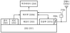
도 2b는 본 발명의 일 실시예에 의한 임피던스 정합장치를 적용한 센서 노드의 구성을 보여준다. 도 2b를 참조하면, 본 발명에 의한 임피던스 정합장치를 적용한 센서 노드는 일반적인 WSN용 센서 노드와 마찬가지로, 전원(201), 센서(202), ADC(203), 액추에이터(204), 메모리(205), 제어부(206), 전송부(207) 및 안테나(209)를 포함한다.Figure 2b shows the configuration of the sensor node applying the impedance matching device according to an embodiment of the present invention. Referring to FIG. 2B, the sensor node to which the impedance matching device according to the present invention is applied is similar to a general WSN sensor node, such as a power supply 201, a
하지만, 본 발명에서는 일반적인 WSN용 센서 노드와 달리 고정임피던스정합부(108)대신에 가변임피던스정합부(208b)를 가지며, 신호세기측정부(210b)를 더 가진다.However, the present invention has a variable impedance matching
본 발명에 의한 임피던스 정합장치를 적용한 센서 노드는 가변임피던스정합부(208b)의 임피던스 값을 조정하면서 전송부(207b)로부터 출력되는 출력 신호의 세기를 신호세기측정부(210b)로 측정한다. 출력 신호의 세기는 전자기장의 크기로 측정할 수 있다.The sensor node to which the impedance matching device according to the present invention is applied measures the intensity of the output signal output from the transmission unit 207b by adjusting the impedance value of the variable impedance matching
제어부(206b)는 출력 신호의 세기가 가장 큰 경우의 임피던스 값을 가지도록 가변임피던스정합부(208b)를 조절한다.The controller 206b adjusts the variable
도 3은 본 발명의 바람직한 일 실시예에 의한 센서 노드에 있어서의 임피던스 정합방법의 흐름을 보여주는 도면이다.3 is a view showing the flow of the impedance matching method in the sensor node according to an embodiment of the present invention.
서로 다른 임피던스값을 가지는 복수개의 임피던스 정합회로 중에서 특정한 임피던스값을 가지는 임피던스 정합회로를 선택하여 임피던스값을 변경(S301)하고, 출력신호의 세기를 측정한다(S302).An impedance matching circuit having a specific impedance value is selected from a plurality of impedance matching circuits having different impedance values to change the impedance value (S301), and the intensity of the output signal is measured (S302).
가능한 모든 임피던스값에 따라 출력신호의 세기 측정을 반복한다(S303).The strength measurement of the output signal is repeated according to all possible impedance values (S303).
임피던스 정합회로가 출력신호의 세기가 최대값이 되는 임피던스값을 가지도록 조절한다(S304).The impedance matching circuit adjusts to have an impedance value at which the intensity of the output signal is the maximum value (S304).
이처럼, 본 발명에 의하면 가변임피던스정합부의 임피던스 값을 조정하면서 전송부로부터 출력되는 출력신호의 세기를 신호세기측정부로 측정하여, 출력되는 출력신호의 세기가 가장 큰 경우의 임피던스 값으로 가변임피던스정합부(208a)의 임피던스값을 조정하여 센서 노드의 전송 효율을 높인다.As described above, according to the present invention, the intensity of the output signal output from the transmitter is measured by the signal intensity measuring unit while adjusting the impedance value of the variable impedance matching unit, and the variable impedance matching unit is set to the impedance value when the intensity of the output signal is the largest. The impedance value of 208a is adjusted to increase the transmission efficiency of the sensor node.
본 발명은 또한 컴퓨터로 읽을 수 있는 기록매체에 컴퓨터가 읽을 수 있는 코드로서 구현하는 것이 가능하다. 컴퓨터가 읽을 수 있는 기록매체는 컴퓨터 시스템에 의하여 읽혀질 수 있는 데이터가 저장되는 모든 종류의 기록장치를 포함한다. 컴퓨터가 읽을 수 있는 기록매체의 예로는 ROM, RAM, CD-ROM, 자기 테이프, 플로피디스크, 광데이터 저장장치 등이 있으며, 또한 캐리어 웨이브(예를 들어 인터넷을 통한 전송)의 형태로 구현되는 것도 포함한다. 또한 컴퓨터가 읽을 수 있는 기록매체는 네트워크로 연결된 컴퓨터 시스템에 분산되어 분산방식으로 컴퓨터가 읽을 수 있는 코드가 저장되고 실행될 수 있다.The invention can also be embodied as computer readable code on a computer readable recording medium. The computer-readable recording medium includes all kinds of recording devices in which data that can be read by a computer system is stored. Examples of computer-readable recording media include ROM, RAM, CD-ROM, magnetic tape, floppy disk, optical data storage, and the like, and may also be implemented in the form of a carrier wave (for example, transmission over the Internet). Include. The computer readable recording medium can also be distributed over network coupled computer systems so that the computer readable code is stored and executed in a distributed fashion.
이제까지 본 발명에 대하여 그 바람직한 실시예들을 중심으로 살펴보았다. 본 발명이 속하는 기술 분야에서 통상의 지식을 가진 자는 본 발명이 본 발명의 본질적인 특성에서 벗어나지 않는 범위에서 변형된 형태로 구현될 수 있음을 이해할 수 있을 것이다. 그러므로 개시된 실시예들은 한정적인 관점이 아니라 설명적인 관점에서 고려되어야 한다. 본 발명의 범위는 전술한 설명이 아니라 특허청구범위에 나타나 있으며, 그와 동등한 범위 내에 있는 모든 차이점은 본 발명에 포함된 것으로 해석되어야 할 것이다.So far I looked at the center of the preferred embodiment for the present invention. Those skilled in the art will appreciate that the present invention can be implemented in a modified form without departing from the essential features of the present invention. Therefore, the disclosed embodiments should be considered in descriptive sense only and not for purposes of limitation. The scope of the present invention is shown in the claims rather than the foregoing description, and all differences within the scope will be construed as being included in the present invention.
본 발명에 의하면 센서 노드의 사용 환경에 따라 달라질 수 있는 전송부와 안테나 사이의 임피던스를 조절하여 센서 노드의 전송 효율을 증대함으로써 센서 노드의 한정된 전원의 사용 시간을 늘리고 주변의 다른 센서 노드들과의 접속 성공률을 높이며, 센서 노드의 통신 신뢰성을 확보된다.According to the present invention, by increasing the transmission efficiency of the sensor node by adjusting the impedance between the transmitter and the antenna, which may vary according to the use environment of the sensor node, the use time of the limited power of the sensor node is increased and other sensor nodes in the vicinity are increased. It increases the connection success rate and secures the communication reliability of the sensor node.
특히, 본 발명은 WSN용 센서 노드가 한정된 전력을 이용하여 저전력 환경에서 사용되는 경우, 안테나와 전송부 사이의 임피던스 정합이 이루어지지 않아 통신 품질이 저하되는 문제를 해결한다.In particular, when the sensor node for the WSN is used in a low power environment using a limited power, the impedance matching between the antenna and the transmission unit is not made to solve the problem of communication quality deterioration.
Claims (7)
Translated fromKoreanPriority Applications (2)
| Application Number | Priority Date | Filing Date | Title |
|---|---|---|---|
| KR1020060125052AKR100833513B1 (en) | 2006-12-08 | 2006-12-08 | Impedance Matching Device and Method in Sensor Node |
| US11/860,388US20080136548A1 (en) | 2006-12-08 | 2007-09-24 | Impedance matching device of sensor node and impedance matching method of sensor node |
Applications Claiming Priority (1)
| Application Number | Priority Date | Filing Date | Title |
|---|---|---|---|
| KR1020060125052AKR100833513B1 (en) | 2006-12-08 | 2006-12-08 | Impedance Matching Device and Method in Sensor Node |
Publications (1)
| Publication Number | Publication Date |
|---|---|
| KR100833513B1true KR100833513B1 (en) | 2008-05-29 |
Family
ID=39497278
Family Applications (1)
| Application Number | Title | Priority Date | Filing Date |
|---|---|---|---|
| KR1020060125052AExpired - Fee RelatedKR100833513B1 (en) | 2006-12-08 | 2006-12-08 | Impedance Matching Device and Method in Sensor Node |
Country Status (2)
| Country | Link |
|---|---|
| US (1) | US20080136548A1 (en) |
| KR (1) | KR100833513B1 (en) |
Cited By (1)
| Publication number | Priority date | Publication date | Assignee | Title |
|---|---|---|---|---|
| KR101041789B1 (en) | 2009-09-22 | 2011-06-17 | 광운대학교 산학협력단 | Operation Method of Wireless Sensor Network Sensor Node to Improve Transmission Efficiency According to Temperature Change |
Families Citing this family (4)
| Publication number | Priority date | Publication date | Assignee | Title |
|---|---|---|---|---|
| US10263572B2 (en)* | 2016-10-05 | 2019-04-16 | Futurewei Technologies, Inc. | Radio frequency apparatus and method with dual variable impedance components |
| KR102314473B1 (en) | 2017-12-12 | 2021-10-19 | 한국전자통신연구원 | Method for controlling transmission signal of communication system on disaster site and apparatus for the same |
| CN114217563A (en)* | 2022-01-14 | 2022-03-22 | 华清科盛(北京)信息技术有限公司 | Terminal resistance adjusting method and device of industrial CAN bus based on sorting system |
| CN115834278A (en)* | 2022-09-22 | 2023-03-21 | 中山水木光华电子信息科技有限公司 | CAN network master station with adjustable matching resistance, system, control method and medium |
Citations (2)
| Publication number | Priority date | Publication date | Assignee | Title |
|---|---|---|---|---|
| KR20050022977A (en)* | 2003-08-28 | 2005-03-09 | 주식회사 팬택앤큐리텔 | Impedence matching apparatus of folder type mobile communication unit |
| KR20060069481A (en)* | 2003-08-29 | 2006-06-21 | 노키아 코포레이션 | Method and apparatus for providing integrated load matching using adaptive power amplifier compensation |
Family Cites Families (9)
| Publication number | Priority date | Publication date | Assignee | Title |
|---|---|---|---|---|
| US4380767A (en)* | 1980-10-27 | 1983-04-19 | Texas Instruments Incorporated | Controlled antenna tuner |
| US6438360B1 (en)* | 1999-07-22 | 2002-08-20 | Motorola, Inc. | Amplifier system with load control to produce an amplitude envelope |
| SE516535C2 (en)* | 1999-10-29 | 2002-01-29 | Allgon Ab | Antenna device switchable between a plurality of configuration modes adapted for use in different operating environments and associated method |
| US6887339B1 (en)* | 2000-09-20 | 2005-05-03 | Applied Science And Technology, Inc. | RF power supply with integrated matching network |
| US7379714B2 (en)* | 2004-04-02 | 2008-05-27 | Interdigital Technology Corporation | Method and apparatus for dynamically adjusting a transmitter's impedance |
| US7528674B2 (en)* | 2005-01-31 | 2009-05-05 | Panasonic Corporation | Mobile radio apparatus capable of adaptive impedance matching |
| US9474564B2 (en)* | 2005-03-31 | 2016-10-25 | Covidien Ag | Method and system for compensating for external impedance of an energy carrying component when controlling an electrosurgical generator |
| US7279979B2 (en)* | 2005-09-12 | 2007-10-09 | Nokia Corporation | Method and arrangement for adjusting an output impedance of a power amplifier |
| US7409245B1 (en)* | 2007-01-30 | 2008-08-05 | Cardiac Pacemakers, Inc. | Variable antenna matching network for an implantable antenna |
- 2006
- 2006-12-08KRKR1020060125052Apatent/KR100833513B1/ennot_activeExpired - Fee Related
- 2007
- 2007-09-24USUS11/860,388patent/US20080136548A1/ennot_activeAbandoned
Patent Citations (2)
| Publication number | Priority date | Publication date | Assignee | Title |
|---|---|---|---|---|
| KR20050022977A (en)* | 2003-08-28 | 2005-03-09 | 주식회사 팬택앤큐리텔 | Impedence matching apparatus of folder type mobile communication unit |
| KR20060069481A (en)* | 2003-08-29 | 2006-06-21 | 노키아 코포레이션 | Method and apparatus for providing integrated load matching using adaptive power amplifier compensation |
Cited By (1)
| Publication number | Priority date | Publication date | Assignee | Title |
|---|---|---|---|---|
| KR101041789B1 (en) | 2009-09-22 | 2011-06-17 | 광운대학교 산학협력단 | Operation Method of Wireless Sensor Network Sensor Node to Improve Transmission Efficiency According to Temperature Change |
Also Published As
| Publication number | Publication date |
|---|---|
| US20080136548A1 (en) | 2008-06-12 |
Similar Documents
| Publication | Publication Date | Title |
|---|---|---|
| US8014802B1 (en) | Transmit power adaptation algorithm using 802.11H | |
| KR101245040B1 (en) | Method for measuring sensitivity of data packet signal receiver | |
| KR100833513B1 (en) | Impedance Matching Device and Method in Sensor Node | |
| US6408193B1 (en) | Cellular telephone | |
| ES2553249T3 (en) | Routing device of a wireless local area access network and its signal transmission method | |
| WO2004082135A2 (en) | Closed loop power control of non-constant envelope waveforms using sample/hold | |
| WO2000025445A1 (en) | Method and apparatus for calibration of a wireless transmitter | |
| US9363130B2 (en) | Dynamic digital predistortion for a microwave radio system | |
| CN112737655A (en) | Communication method, system and device based on intelligent reflecting surface | |
| KR100645427B1 (en) | OPM receiver which forms uneven beam width according to channel characteristics, communication device and method using the same | |
| US7224215B2 (en) | Intelligent RF power control for wireless modem devices | |
| US20010050963A1 (en) | Diversity type transmitter having system for controlling the delay time of each of plural transmission units | |
| JP2005109665A (en) | Load drive device | |
| US7653365B2 (en) | Method for controlling signal power in transmitter of radio system by weighting, and transmitter therefor | |
| JP3643217B2 (en) | System for evaluating electromagnetic field environment characteristics of wireless terminals | |
| WO2025027079A1 (en) | Methods, readers and tags | |
| Varshney | Making Low-Power and Long-Range Wireless Backscatter Transmitters | |
| US20240429969A1 (en) | Reconfigurable intelligent surface, communication method using the reconfigurable intelligent surface, and transceiver device including the reconfigurable intelligent surface | |
| JP7232211B2 (en) | Signal generator and signal generation method | |
| US20210218448A1 (en) | Wireless location-sensing | |
| KR100493211B1 (en) | BTS remote watch-control system and method connected a beacon | |
| Rodriguez | Pushing the Limits of RF and Underwater Backscatter Systems | |
| KR200290690Y1 (en) | BTS remote watch-control system connected a beacon | |
| CN120415523A (en) | A cross-media communication method and device based on passive relay | |
| JP2020036137A (en) | Wireless device |
Legal Events
| Date | Code | Title | Description |
|---|---|---|---|
| A201 | Request for examination | ||
| PA0109 | Patent application | St.27 status event code:A-0-1-A10-A12-nap-PA0109 | |
| PA0201 | Request for examination | St.27 status event code:A-1-2-D10-D11-exm-PA0201 | |
| E902 | Notification of reason for refusal | ||
| PE0902 | Notice of grounds for rejection | St.27 status event code:A-1-2-D10-D21-exm-PE0902 | |
| P11-X000 | Amendment of application requested | St.27 status event code:A-2-2-P10-P11-nap-X000 | |
| P13-X000 | Application amended | St.27 status event code:A-2-2-P10-P13-nap-X000 | |
| E701 | Decision to grant or registration of patent right | ||
| PE0701 | Decision of registration | St.27 status event code:A-1-2-D10-D22-exm-PE0701 | |
| GRNT | Written decision to grant | ||
| PR0701 | Registration of establishment | St.27 status event code:A-2-4-F10-F11-exm-PR0701 | |
| PR1002 | Payment of registration fee | St.27 status event code:A-2-2-U10-U11-oth-PR1002 Fee payment year number:1 | |
| PG1601 | Publication of registration | St.27 status event code:A-4-4-Q10-Q13-nap-PG1601 | |
| PN2301 | Change of applicant | St.27 status event code:A-5-5-R10-R13-asn-PN2301 St.27 status event code:A-5-5-R10-R11-asn-PN2301 | |
| FPAY | Annual fee payment | Payment date:20110511 Year of fee payment:4 | |
| PR1001 | Payment of annual fee | St.27 status event code:A-4-4-U10-U11-oth-PR1001 Fee payment year number:4 | |
| LAPS | Lapse due to unpaid annual fee | ||
| PC1903 | Unpaid annual fee | St.27 status event code:A-4-4-U10-U13-oth-PC1903 Not in force date:20120524 Payment event data comment text:Termination Category : DEFAULT_OF_REGISTRATION_FEE | |
| PC1903 | Unpaid annual fee | St.27 status event code:N-4-6-H10-H13-oth-PC1903 Ip right cessation event data comment text:Termination Category : DEFAULT_OF_REGISTRATION_FEE Not in force date:20120524 | |
| PN2301 | Change of applicant | St.27 status event code:A-5-5-R10-R13-asn-PN2301 St.27 status event code:A-5-5-R10-R11-asn-PN2301 |