KR100833424B1 - Metal wiring manufacturing method of semiconductor memory device - Google Patents
Metal wiring manufacturing method of semiconductor memory deviceDownload PDFInfo
- Publication number
- KR100833424B1 KR100833424B1KR1020060060600AKR20060060600AKR100833424B1KR 100833424 B1KR100833424 B1KR 100833424B1KR 1020060060600 AKR1020060060600 AKR 1020060060600AKR 20060060600 AKR20060060600 AKR 20060060600AKR 100833424 B1KR100833424 B1KR 100833424B1
- Authority
- KR
- South Korea
- Prior art keywords
- film
- metal film
- forming
- memory device
- semiconductor memory
- Prior art date
- Legal status (The legal status is an assumption and is not a legal conclusion. Google has not performed a legal analysis and makes no representation as to the accuracy of the status listed.)
- Expired - Fee Related
Links
Images


Classifications
- H—ELECTRICITY
- H01—ELECTRIC ELEMENTS
- H01L—SEMICONDUCTOR DEVICES NOT COVERED BY CLASS H10
- H01L21/00—Processes or apparatus adapted for the manufacture or treatment of semiconductor or solid state devices or of parts thereof
- H01L21/70—Manufacture or treatment of devices consisting of a plurality of solid state components formed in or on a common substrate or of parts thereof; Manufacture of integrated circuit devices or of parts thereof
- H01L21/71—Manufacture of specific parts of devices defined in group H01L21/70
- H01L21/768—Applying interconnections to be used for carrying current between separate components within a device comprising conductors and dielectrics
- H01L21/76801—Applying interconnections to be used for carrying current between separate components within a device comprising conductors and dielectrics characterised by the formation and the after-treatment of the dielectrics, e.g. smoothing
- H01L21/76829—Applying interconnections to be used for carrying current between separate components within a device comprising conductors and dielectrics characterised by the formation and the after-treatment of the dielectrics, e.g. smoothing characterised by the formation of thin functional dielectric layers, e.g. dielectric etch-stop, barrier, capping or liner layers
- H01L21/76834—Applying interconnections to be used for carrying current between separate components within a device comprising conductors and dielectrics characterised by the formation and the after-treatment of the dielectrics, e.g. smoothing characterised by the formation of thin functional dielectric layers, e.g. dielectric etch-stop, barrier, capping or liner layers formation of thin insulating films on the sidewalls or on top of conductors
- H—ELECTRICITY
- H01—ELECTRIC ELEMENTS
- H01L—SEMICONDUCTOR DEVICES NOT COVERED BY CLASS H10
- H01L21/00—Processes or apparatus adapted for the manufacture or treatment of semiconductor or solid state devices or of parts thereof
- H01L21/02—Manufacture or treatment of semiconductor devices or of parts thereof
- H01L21/04—Manufacture or treatment of semiconductor devices or of parts thereof the devices having potential barriers, e.g. a PN junction, depletion layer or carrier concentration layer
- H01L21/18—Manufacture or treatment of semiconductor devices or of parts thereof the devices having potential barriers, e.g. a PN junction, depletion layer or carrier concentration layer the devices having semiconductor bodies comprising elements of Group IV of the Periodic Table or AIIIBV compounds with or without impurities, e.g. doping materials
- H01L21/30—Treatment of semiconductor bodies using processes or apparatus not provided for in groups H01L21/20 - H01L21/26
- H01L21/31—Treatment of semiconductor bodies using processes or apparatus not provided for in groups H01L21/20 - H01L21/26 to form insulating layers thereon, e.g. for masking or by using photolithographic techniques; After treatment of these layers; Selection of materials for these layers
- H01L21/3205—Deposition of non-insulating-, e.g. conductive- or resistive-, layers on insulating layers; After-treatment of these layers
- H01L21/321—After treatment
- H01L21/3213—Physical or chemical etching of the layers, e.g. to produce a patterned layer from a pre-deposited extensive layer
- H01L21/32139—Physical or chemical etching of the layers, e.g. to produce a patterned layer from a pre-deposited extensive layer using masks
- H—ELECTRICITY
- H01—ELECTRIC ELEMENTS
- H01L—SEMICONDUCTOR DEVICES NOT COVERED BY CLASS H10
- H01L21/00—Processes or apparatus adapted for the manufacture or treatment of semiconductor or solid state devices or of parts thereof
- H01L21/70—Manufacture or treatment of devices consisting of a plurality of solid state components formed in or on a common substrate or of parts thereof; Manufacture of integrated circuit devices or of parts thereof
- H01L21/71—Manufacture of specific parts of devices defined in group H01L21/70
- H01L21/768—Applying interconnections to be used for carrying current between separate components within a device comprising conductors and dielectrics
- H01L21/76801—Applying interconnections to be used for carrying current between separate components within a device comprising conductors and dielectrics characterised by the formation and the after-treatment of the dielectrics, e.g. smoothing
- H01L21/76837—Filling up the space between adjacent conductive structures; Gap-filling properties of dielectrics
Landscapes
- Engineering & Computer Science (AREA)
- Physics & Mathematics (AREA)
- Condensed Matter Physics & Semiconductors (AREA)
- General Physics & Mathematics (AREA)
- Manufacturing & Machinery (AREA)
- Computer Hardware Design (AREA)
- Microelectronics & Electronic Packaging (AREA)
- Power Engineering (AREA)
- Internal Circuitry In Semiconductor Integrated Circuit Devices (AREA)
- Semiconductor Memories (AREA)
Abstract
Translated fromKoreanDescription
Translated fromKorean도 1 내지 도 6은 본 발명의 반도체 메모리 소자의 금속배선 제조방법을 순차적으로 도시한 단면도이다.1 to 6 are cross-sectional views sequentially illustrating a method for manufacturing metal wiring of the semiconductor memory device of the present invention.
<도면의 주요 부분에 대한 부호의 설명><Explanation of symbols for the main parts of the drawings>
101 : 반도체 기판102 : 하부층101
103 : 제 1 층간 절연막104 : 플러그103: first interlayer insulating film 104: plug
105 : 베리어 메탈막106 : 메탈층105: barrier metal film 106: metal layer
107 : 반사 방지막108 : 제 1 질화막107: antireflection film 108: first nitride film
109 : 카본막110 : 제 2 질화막109: carbon film 110: second nitride film
111 : 포토 레지스트 패턴112 : 절연막111: photoresist pattern 112: insulating film
113 : 제 2 층간 절연막113: second interlayer insulating film
본 발명은 반도체 메모리 소자에 관한 것으로 특히, 반도체 메모리 소자의 금속배선 제조방법에 관한 것이다.BACKGROUND OF THE INVENTION 1. Field of the Invention The present invention relates to semiconductor memory devices, and more particularly, to a method for manufacturing metal wiring of semiconductor memory devices.
플래쉬 메모리 소자의 금속배선 형성 방법으로 텅스텐(W)을 플러그로 사용하는 다마신 구조 형성 방법이 사용되어 왔다. 소자의 집적도가 커짐에 따라 디자인 룰(design rule)이 감소되고 이에 따라, 라인을 형성하는 패턴간의 공간이 줄어들어서 캐패시턴스(capacitance) 값 확보에 어려움이 발생한다. 캐패시턴스 문제를 해결하기 위해서는 계면접합 공정에서 메탈(metal)층의 높이를 낮추어 캐패시턴스 값을 줄여주어야 한다. 하지만, 낮아진 메탈층의 높이로 인해 저항값이 증가하게 된다. 따라서, 메탈층의 높이를 줄여 캐패시턴스 값을 확보하면서 저항값의 변화를 주지 않기 위해서는 낮은 비저항 특성을 가진 물질을 계면에 형성하면 된다. 낮은 비저항 특성을 지닌 물질로는 로직(logic)에서 사용중인 구리(Cu) 또는 와이어(wire) 물질로 사용중인 알루미늄(Al) 등이 있다. 하지만, 텅스텐 다마신 공정과 같이 후속 평탄화공정(CMP)의 슬러리(slurry) 문제로 인하여 알루미늄을 사용하기가 어렵다.As a method of forming a metal wiring of a flash memory device, a damascene structure forming method using tungsten (W) as a plug has been used. As the degree of integration of the device increases, a design rule decreases, and thus, a space between patterns forming lines decreases, thereby making it difficult to secure a capacitance value. In order to solve the capacitance problem, it is necessary to reduce the capacitance value by lowering the height of the metal layer in the interfacial bonding process. However, the resistance value is increased due to the lower height of the metal layer. Therefore, in order to reduce the height of the metal layer to secure the capacitance value and not to change the resistance value, a material having a low specific resistance may be formed at the interface. Materials having low resistivity include copper (Cu) used in logic or aluminum (Al) used as a wire material. However, aluminum is difficult to use due to slurry problems in subsequent planarization processes (CMP), such as tungsten damascene process.
이에 대한 방안으로 알루미늄 형성 후 RIE(reactive ion etching) 방식을 사용하여 패턴 형성을 시도하고 있다. 이러한 알루미늄 RIE 방식은 베리어메탈막 형성 후 알루미늄 및 반사방지막이 순차적으로 적층되는 방식으로 형성된다. 그러나, 상기 방식은 후속 식각 공정에서 물질에 따른 식각 비율차이 또는 과도 식각으로 인하여 알루미늄 메탈층의 측벽 손상을 유발한다. 또한, 측벽 손상으로 인해 유전물질 형성시 보이드(void)가 발생하여 신뢰도가 떨어진다.As a solution for this, after the aluminum is formed, an attempt is made to form a pattern using a reactive ion etching (RIE) method. The aluminum RIE method is formed in such a manner that aluminum and an antireflection film are sequentially stacked after the barrier metal film is formed. However, this approach causes sidewall damage of the aluminum metal layer due to etch rate differences or excessive etching depending on the material in subsequent etching processes. In addition, due to sidewall damage, voids are generated when the dielectric material is formed, thereby reducing reliability.
따라서, 본 발명은 메탈막을 보호하는 스페이서층을 형성함으로써 식각 공정시 메탈막의 손실을 방지할 수 있는 반도체 메모리 소자의 금속배선 제조방법을 제공하는 데 있다.Accordingly, an aspect of the present invention is to provide a method for manufacturing a metal wiring of a semiconductor memory device capable of preventing a loss of a metal film during an etching process by forming a spacer layer protecting the metal film.
본 발명은 반도체 메모리 소자의 금속배선 제조방법에 대한 것으로, 반도체 기판 상부의 제 1 층간 절연막에 다마신 구조의 플러그를 형성하는 단계, 결과물 상부에 베리어 메탈막, 메탈막 및 반사 방지막을 순차적으로 형성하는 단계, 반사 방지막, 메탈막 및 베리어 메탈막을 소정의 패턴을 사용하여 식각하는 단계 및 메탈막의 측벽에 절연막을 형성하는 단계를 포함하는 반도체 메모리 소자의 금속배선 제조방법을 포함한다.The present invention relates to a method for manufacturing a metal wiring of a semiconductor memory device, comprising the steps of: forming a plug having a damascene structure in a first interlayer insulating film on a semiconductor substrate, and sequentially forming a barrier metal film, a metal film, and an anti-reflection film on the resultant And etching the anti-reflection film, the metal film, and the barrier metal film by using a predetermined pattern, and forming an insulating film on the sidewall of the metal film.
이하, 첨부된 도면을 참조하여 본 발명의 바람직한 실시예를 설명하기로 한다. 그러나, 본 발명은 이하에서 개시되는 실시예에 한정되는 것이 아니라 서로 다른 다양한 형태로 구현될 수 있으며, 단지 본 실시예는 본 발명의 개시가 완전하도록 하며 통상의 지식을 가진자에게 발명의 범주를 완전하게 알려주기 위해 제공되는 것이다.Hereinafter, with reference to the accompanying drawings will be described a preferred embodiment of the present invention. However, the present invention is not limited to the embodiments disclosed below, but can be implemented in various forms, and only the present embodiments are intended to complete the disclosure of the present invention and to those skilled in the art. It is provided for complete information.
도 1 내지 도 6은 본 발명의 반도체 메모리 소자의 금속배선 제조방법을 순 차적으로 도시한 단면도이다.1 to 6 are cross-sectional views sequentially illustrating a method for manufacturing metal wiring of a semiconductor memory device of the present invention.
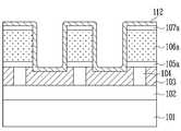
도 1을 참조하면, 반도체 기판(101) 상부에 게이트 등을 포함하는 하부층(102)을 형성한다. 하부층(102) 상부에 제 1 층간 절연막(103)을 형성하고, 다마신 구조의 플러그(104)를 형성한다. 전체구조 상부에 베리어 메탈막(105), 메탈층(106) 및 반사 방지막(107)을 순차적으로 형성한다. 베리어 메탈막(105)은 스퍼터(sputtering) 방식으로 형성하고, 형성 물질은 Ti 및 TiN을 사용한다. 금속배선을 위한 메탈층(106) 물질은 알루미늄(Al)을 사용하여 형성한다. 반사 방지막(107) 형성 물질은 Ti 및 TiN을 사용하여 인시추(in-situ)로 형성한다.Referring to FIG. 1, a
도 2를 참조하면, 반사 방지막(107) 상부에 제 1 질화막(108), α-카본막(109), 제 2 질화막(110) 및 포토 레지스트 패턴(111)을 순차적으로 형성한다. 제 1 및 제 2 질화막(108 및 110) 형성 물질은 SiON을 사용하여 형성한다. 포토레지스트 패턴(111)에 따라 식각 공정을 실시한다.Referring to FIG. 2, the
도 3을 참조하면, 소정의 식각 공정을 통해 베리어 메탈 패턴(105a) 까지 형성하고, 제 1 질화막(108), 카본막(109), 제 2 질화막(110) 및 포토 레지스트 패턴(111)을 제거한다.Referring to FIG. 3, the
도 4를 참조하면, 전체구조의 표면을 따라 절연막(112)을 형성한다. 절연막(112) 형성 물질은 질화막 또는 산화막을 사용하여 형성할 수 있다. 두께는 20 내지 200Å으로 형성하는 것이 바람직하다.Referring to FIG. 4, an
도 5를 참조하면, 패턴간 브릿지(bridge) 현상을 방지하기 위해 절연막(112)을 식각 하는데 패턴 측벽에 스페이서용으로 절연막(112a)을 남긴다. 이때, 제1 층간 절연막(103)이 드러나도록 오버식각(over etching) 공정을 실시하는 것이 바람직하며, 식각되는 깊이는 50Å 내지 500Å 가 되도록 하는 것이 바람직하다.Referring to FIG. 5, the
도 6을 참조하면, 전체구조 상부에 제 2 층간 절연막(113)을 형성하는 갭필(gap-fill) 공정을 실시한다. 제 2 층간 절연막(113)은 HDP(high density plasma) 산화막으로 형성할 수 있다. 특히, 제 2 층간 절연막(113)을 형성하는 공정 시, 잔류된 절연막(112a)이 메탈층 패턴(106a)의 측벽을 보호하므로 플라즈마(plasma)로 인한 금속배선의 저항증가를 억제할 수 있다.Referring to FIG. 6, a gap-fill process of forming a second
상기에서 설명한 본 발명의 기술적 사상은 바람직한 실시예에서 구체적으로 기술되었으나, 상기한 실시예는 그 설명을 위한 것이며 그 제한을 위한 것이 아님을 주의하여야 한다. 또한, 본 발명은 본 발명의 기술 분야의 통상의 전문가라면 본 발명의 기술적 사상의 범위 내에서 다양한 실시예가 가능함을 이해할 수 있을 것이다.Although the technical spirit of the present invention described above has been described in detail in a preferred embodiment, it should be noted that the above-described embodiment is for the purpose of description and not of limitation. In addition, the present invention will be understood by those skilled in the art that various embodiments are possible within the scope of the technical idea of the present invention.
이상에서 설명한 바와 같이, 본 발명에 따른 반도체 메모리 소자의 금속배선 제조방법은 메탈막을 보호하는 스페이서층을 형성하여 식각 공정시 메탈막의 손실을 방지함으로써 금속배선 프로파일을 개선하고 후속 갭필 공정시 보이드 발생을 방지할 수 있다.As described above, the metallization manufacturing method of the semiconductor memory device according to the present invention forms a spacer layer to protect the metal layer to prevent the loss of the metal layer during the etching process to improve the metallization profile and to generate voids during the subsequent gap fill process. You can prevent it.
Claims (7)
Translated fromKoreanPriority Applications (2)
| Application Number | Priority Date | Filing Date | Title |
|---|---|---|---|
| KR1020060060600AKR100833424B1 (en) | 2006-06-30 | 2006-06-30 | Metal wiring manufacturing method of semiconductor memory device |
| US11/647,087US7557033B2 (en) | 2006-06-30 | 2006-12-27 | Method of forming metal line of semiconductor memory device |
Applications Claiming Priority (1)
| Application Number | Priority Date | Filing Date | Title |
|---|---|---|---|
| KR1020060060600AKR100833424B1 (en) | 2006-06-30 | 2006-06-30 | Metal wiring manufacturing method of semiconductor memory device |
Publications (2)
| Publication Number | Publication Date |
|---|---|
| KR20080002043A KR20080002043A (en) | 2008-01-04 |
| KR100833424B1true KR100833424B1 (en) | 2008-05-29 |
Family
ID=38877242
Family Applications (1)
| Application Number | Title | Priority Date | Filing Date |
|---|---|---|---|
| KR1020060060600AExpired - Fee RelatedKR100833424B1 (en) | 2006-06-30 | 2006-06-30 | Metal wiring manufacturing method of semiconductor memory device |
Country Status (2)
| Country | Link |
|---|---|
| US (1) | US7557033B2 (en) |
| KR (1) | KR100833424B1 (en) |
Families Citing this family (2)
| Publication number | Priority date | Publication date | Assignee | Title |
|---|---|---|---|---|
| CN115241072B (en)* | 2021-04-23 | 2025-02-21 | 长鑫存储技术有限公司 | Semiconductor packaging structure and method for forming the same |
| US11978698B2 (en)* | 2021-04-23 | 2024-05-07 | Changxin Memory Technologies, Inc. | Method for forming a semiconductor package structure |
Citations (3)
| Publication number | Priority date | Publication date | Assignee | Title |
|---|---|---|---|---|
| KR20020078623A (en) | 2001-04-06 | 2002-10-19 | 주식회사 하이닉스반도체 | Method for forming the line in semiconductor device |
| KR20040001855A (en) | 2002-06-29 | 2004-01-07 | 주식회사 하이닉스반도체 | Method for fabricating of Memory device with Hydrogen barrier |
| KR20060072217A (en)* | 2004-12-22 | 2006-06-28 | 동부일렉트로닉스 주식회사 | Metal wiring formation method of semiconductor device |
Family Cites Families (3)
| Publication number | Priority date | Publication date | Assignee | Title |
|---|---|---|---|---|
| JP2001250867A (en)* | 2000-03-07 | 2001-09-14 | Fujitsu Ltd | Semiconductor device and manufacturing method thereof |
| JP3485110B2 (en)* | 2001-07-25 | 2004-01-13 | セイコーエプソン株式会社 | Semiconductor device |
| KR100519799B1 (en)* | 2004-03-25 | 2005-10-10 | 삼성전자주식회사 | fuse rigion of semiconductor device and method of fabricating the same |
- 2006
- 2006-06-30KRKR1020060060600Apatent/KR100833424B1/ennot_activeExpired - Fee Related
- 2006-12-27USUS11/647,087patent/US7557033B2/ennot_activeExpired - Fee Related
Patent Citations (3)
| Publication number | Priority date | Publication date | Assignee | Title |
|---|---|---|---|---|
| KR20020078623A (en) | 2001-04-06 | 2002-10-19 | 주식회사 하이닉스반도체 | Method for forming the line in semiconductor device |
| KR20040001855A (en) | 2002-06-29 | 2004-01-07 | 주식회사 하이닉스반도체 | Method for fabricating of Memory device with Hydrogen barrier |
| KR20060072217A (en)* | 2004-12-22 | 2006-06-28 | 동부일렉트로닉스 주식회사 | Metal wiring formation method of semiconductor device |
Also Published As
| Publication number | Publication date |
|---|---|
| US7557033B2 (en) | 2009-07-07 |
| KR20080002043A (en) | 2008-01-04 |
| US20080003814A1 (en) | 2008-01-03 |
Similar Documents
| Publication | Publication Date | Title |
|---|---|---|
| CN106935544B (en) | Semiconductor device and method for forming the same | |
| CN100576494C (en) | Method for forming dual damascene wiring of semiconductor device using protective via capping layer | |
| CN100399542C (en) | Inner wiring structure and method of forming the same | |
| CN105428308A (en) | Methods for Fabricating Semiconductor Devices Using Liner Layers to Avoid Damage to Underlying Patterns | |
| TW200303599A (en) | Manufacturing method of semiconductor device | |
| US7176123B2 (en) | Method for manufacturing metal line of semiconductor device | |
| JP5047504B2 (en) | Method for manufacturing dual damascene wiring of semiconductor device using via capping protective film | |
| JP2008047582A (en) | Semiconductor device manufacturing method and semiconductor device | |
| KR100833424B1 (en) | Metal wiring manufacturing method of semiconductor memory device | |
| JP2006179515A (en) | Method for manufacturing semiconductor element and etching method | |
| KR20080030292A (en) | Metal wiring formation method of semiconductor device | |
| CN104377160B (en) | Metal interconnection structure and its technology | |
| KR20060005176A (en) | Metal wiring formation method of semiconductor device | |
| KR100876532B1 (en) | Manufacturing Method of Semiconductor Device | |
| TWI512894B (en) | Metal interconnect structure and process thereof | |
| KR101081851B1 (en) | Method of forming a dual damascene pattern in a semiconductor device | |
| KR100745058B1 (en) | Self-aligned contact hole formation method of semiconductor device | |
| KR100827483B1 (en) | Metal wiring formation method of semiconductor device | |
| KR101181271B1 (en) | Method for Forming Metal Line of Semiconductor Device | |
| KR100784074B1 (en) | Bit line formation method of semiconductor device | |
| KR100664788B1 (en) | Metal film planarization method of semiconductor device | |
| JP4876231B2 (en) | Manufacturing method of semiconductor device | |
| KR100979245B1 (en) | Method of manufacturing semiconductor device | |
| KR100587140B1 (en) | Dual damascene pattern formation method of semiconductor device | |
| KR100784105B1 (en) | Manufacturing Method of Semiconductor Device |
Legal Events
| Date | Code | Title | Description |
|---|---|---|---|
| PA0109 | Patent application | St.27 status event code:A-0-1-A10-A12-nap-PA0109 | |
| A201 | Request for examination | ||
| PA0201 | Request for examination | St.27 status event code:A-1-2-D10-D11-exm-PA0201 | |
| D13-X000 | Search requested | St.27 status event code:A-1-2-D10-D13-srh-X000 | |
| D14-X000 | Search report completed | St.27 status event code:A-1-2-D10-D14-srh-X000 | |
| PG1501 | Laying open of application | St.27 status event code:A-1-1-Q10-Q12-nap-PG1501 | |
| E902 | Notification of reason for refusal | ||
| PE0902 | Notice of grounds for rejection | St.27 status event code:A-1-2-D10-D21-exm-PE0902 | |
| P11-X000 | Amendment of application requested | St.27 status event code:A-2-2-P10-P11-nap-X000 | |
| P13-X000 | Application amended | St.27 status event code:A-2-2-P10-P13-nap-X000 | |
| E701 | Decision to grant or registration of patent right | ||
| PE0701 | Decision of registration | St.27 status event code:A-1-2-D10-D22-exm-PE0701 | |
| GRNT | Written decision to grant | ||
| PR0701 | Registration of establishment | St.27 status event code:A-2-4-F10-F11-exm-PR0701 | |
| PR1002 | Payment of registration fee | St.27 status event code:A-2-2-U10-U11-oth-PR1002 Fee payment year number:1 | |
| PG1601 | Publication of registration | St.27 status event code:A-4-4-Q10-Q13-nap-PG1601 | |
| PR1001 | Payment of annual fee | St.27 status event code:A-4-4-U10-U11-oth-PR1001 Fee payment year number:4 | |
| PN2301 | Change of applicant | St.27 status event code:A-5-5-R10-R13-asn-PN2301 St.27 status event code:A-5-5-R10-R11-asn-PN2301 | |
| FPAY | Annual fee payment | Payment date:20120424 Year of fee payment:5 | |
| PR1001 | Payment of annual fee | St.27 status event code:A-4-4-U10-U11-oth-PR1001 Fee payment year number:5 | |
| PN2301 | Change of applicant | St.27 status event code:A-5-5-R10-R13-asn-PN2301 St.27 status event code:A-5-5-R10-R11-asn-PN2301 | |
| LAPS | Lapse due to unpaid annual fee | ||
| PC1903 | Unpaid annual fee | St.27 status event code:A-4-4-U10-U13-oth-PC1903 Not in force date:20130523 Payment event data comment text:Termination Category : DEFAULT_OF_REGISTRATION_FEE | |
| PC1903 | Unpaid annual fee | St.27 status event code:N-4-6-H10-H13-oth-PC1903 Ip right cessation event data comment text:Termination Category : DEFAULT_OF_REGISTRATION_FEE Not in force date:20130523 | |
| PN2301 | Change of applicant | St.27 status event code:A-5-5-R10-R13-asn-PN2301 St.27 status event code:A-5-5-R10-R11-asn-PN2301 | |
| P22-X000 | Classification modified | St.27 status event code:A-4-4-P10-P22-nap-X000 | |
| P22-X000 | Classification modified | St.27 status event code:A-4-4-P10-P22-nap-X000 |