KR100832298B1 - Pattern forming resist and soft mold manufacturing method using the same - Google Patents
Pattern forming resist and soft mold manufacturing method using the sameDownload PDFInfo
- Publication number
- KR100832298B1 KR100832298B1KR1020060059968AKR20060059968AKR100832298B1KR 100832298 B1KR100832298 B1KR 100832298B1KR 1020060059968 AKR1020060059968 AKR 1020060059968AKR 20060059968 AKR20060059968 AKR 20060059968AKR 100832298 B1KR100832298 B1KR 100832298B1
- Authority
- KR
- South Korea
- Prior art keywords
- pattern
- pattern forming
- resist
- forming resist
- soft mold
- Prior art date
- Legal status (The legal status is an assumption and is not a legal conclusion. Google has not performed a legal analysis and makes no representation as to the accuracy of the status listed.)
- Active
Links
Images


Classifications
- B—PERFORMING OPERATIONS; TRANSPORTING
- B29—WORKING OF PLASTICS; WORKING OF SUBSTANCES IN A PLASTIC STATE IN GENERAL
- B29C—SHAPING OR JOINING OF PLASTICS; SHAPING OF MATERIAL IN A PLASTIC STATE, NOT OTHERWISE PROVIDED FOR; AFTER-TREATMENT OF THE SHAPED PRODUCTS, e.g. REPAIRING
- B29C33/00—Moulds or cores; Details thereof or accessories therefor
- B29C33/38—Moulds or cores; Details thereof or accessories therefor characterised by the material or the manufacturing process
- B29C33/40—Plastics, e.g. foam or rubber
- B—PERFORMING OPERATIONS; TRANSPORTING
- B29—WORKING OF PLASTICS; WORKING OF SUBSTANCES IN A PLASTIC STATE IN GENERAL
- B29C—SHAPING OR JOINING OF PLASTICS; SHAPING OF MATERIAL IN A PLASTIC STATE, NOT OTHERWISE PROVIDED FOR; AFTER-TREATMENT OF THE SHAPED PRODUCTS, e.g. REPAIRING
- B29C33/00—Moulds or cores; Details thereof or accessories therefor
- B29C33/38—Moulds or cores; Details thereof or accessories therefor characterised by the material or the manufacturing process
- B29C33/3842—Manufacturing moulds, e.g. shaping the mould surface by machining
- B29C33/3857—Manufacturing moulds, e.g. shaping the mould surface by machining by making impressions of one or more parts of models, e.g. shaped articles and including possible subsequent assembly of the parts
- G—PHYSICS
- G02—OPTICS
- G02F—OPTICAL DEVICES OR ARRANGEMENTS FOR THE CONTROL OF LIGHT BY MODIFICATION OF THE OPTICAL PROPERTIES OF THE MEDIA OF THE ELEMENTS INVOLVED THEREIN; NON-LINEAR OPTICS; FREQUENCY-CHANGING OF LIGHT; OPTICAL LOGIC ELEMENTS; OPTICAL ANALOGUE/DIGITAL CONVERTERS
- G02F1/00—Devices or arrangements for the control of the intensity, colour, phase, polarisation or direction of light arriving from an independent light source, e.g. switching, gating or modulating; Non-linear optics
- G02F1/01—Devices or arrangements for the control of the intensity, colour, phase, polarisation or direction of light arriving from an independent light source, e.g. switching, gating or modulating; Non-linear optics for the control of the intensity, phase, polarisation or colour
- G02F1/13—Devices or arrangements for the control of the intensity, colour, phase, polarisation or direction of light arriving from an independent light source, e.g. switching, gating or modulating; Non-linear optics for the control of the intensity, phase, polarisation or colour based on liquid crystals, e.g. single liquid crystal display cells
- G02F1/1303—Apparatus specially adapted to the manufacture of LCDs
- G—PHYSICS
- G02—OPTICS
- G02F—OPTICAL DEVICES OR ARRANGEMENTS FOR THE CONTROL OF LIGHT BY MODIFICATION OF THE OPTICAL PROPERTIES OF THE MEDIA OF THE ELEMENTS INVOLVED THEREIN; NON-LINEAR OPTICS; FREQUENCY-CHANGING OF LIGHT; OPTICAL LOGIC ELEMENTS; OPTICAL ANALOGUE/DIGITAL CONVERTERS
- G02F1/00—Devices or arrangements for the control of the intensity, colour, phase, polarisation or direction of light arriving from an independent light source, e.g. switching, gating or modulating; Non-linear optics
- G02F1/01—Devices or arrangements for the control of the intensity, colour, phase, polarisation or direction of light arriving from an independent light source, e.g. switching, gating or modulating; Non-linear optics for the control of the intensity, phase, polarisation or colour
- G02F1/13—Devices or arrangements for the control of the intensity, colour, phase, polarisation or direction of light arriving from an independent light source, e.g. switching, gating or modulating; Non-linear optics for the control of the intensity, phase, polarisation or colour based on liquid crystals, e.g. single liquid crystal display cells
- G02F1/133—Constructional arrangements; Operation of liquid crystal cells; Circuit arrangements
- G02F1/1333—Constructional arrangements; Manufacturing methods
- G02F1/1339—Gaskets; Spacers; Sealing of cells
- G02F1/13394—Gaskets; Spacers; Sealing of cells spacers regularly patterned on the cell subtrate, e.g. walls, pillars
- G—PHYSICS
- G02—OPTICS
- G02F—OPTICAL DEVICES OR ARRANGEMENTS FOR THE CONTROL OF LIGHT BY MODIFICATION OF THE OPTICAL PROPERTIES OF THE MEDIA OF THE ELEMENTS INVOLVED THEREIN; NON-LINEAR OPTICS; FREQUENCY-CHANGING OF LIGHT; OPTICAL LOGIC ELEMENTS; OPTICAL ANALOGUE/DIGITAL CONVERTERS
- G02F1/00—Devices or arrangements for the control of the intensity, colour, phase, polarisation or direction of light arriving from an independent light source, e.g. switching, gating or modulating; Non-linear optics
- G02F1/01—Devices or arrangements for the control of the intensity, colour, phase, polarisation or direction of light arriving from an independent light source, e.g. switching, gating or modulating; Non-linear optics for the control of the intensity, phase, polarisation or colour
- G02F1/13—Devices or arrangements for the control of the intensity, colour, phase, polarisation or direction of light arriving from an independent light source, e.g. switching, gating or modulating; Non-linear optics for the control of the intensity, phase, polarisation or colour based on liquid crystals, e.g. single liquid crystal display cells
- G02F1/133—Constructional arrangements; Operation of liquid crystal cells; Circuit arrangements
- G02F1/136—Liquid crystal cells structurally associated with a semi-conducting layer or substrate, e.g. cells forming part of an integrated circuit
- G—PHYSICS
- G03—PHOTOGRAPHY; CINEMATOGRAPHY; ANALOGOUS TECHNIQUES USING WAVES OTHER THAN OPTICAL WAVES; ELECTROGRAPHY; HOLOGRAPHY
- G03F—PHOTOMECHANICAL PRODUCTION OF TEXTURED OR PATTERNED SURFACES, e.g. FOR PRINTING, FOR PROCESSING OF SEMICONDUCTOR DEVICES; MATERIALS THEREFOR; ORIGINALS THEREFOR; APPARATUS SPECIALLY ADAPTED THEREFOR
- G03F7/00—Photomechanical, e.g. photolithographic, production of textured or patterned surfaces, e.g. printing surfaces; Materials therefor, e.g. comprising photoresists; Apparatus specially adapted therefor
- G03F7/0005—Production of optical devices or components in so far as characterised by the lithographic processes or materials used therefor
- G03F7/0007—Filters, e.g. additive colour filters; Components for display devices
- G—PHYSICS
- G03—PHOTOGRAPHY; CINEMATOGRAPHY; ANALOGOUS TECHNIQUES USING WAVES OTHER THAN OPTICAL WAVES; ELECTROGRAPHY; HOLOGRAPHY
- G03F—PHOTOMECHANICAL PRODUCTION OF TEXTURED OR PATTERNED SURFACES, e.g. FOR PRINTING, FOR PROCESSING OF SEMICONDUCTOR DEVICES; MATERIALS THEREFOR; ORIGINALS THEREFOR; APPARATUS SPECIALLY ADAPTED THEREFOR
- G03F7/00—Photomechanical, e.g. photolithographic, production of textured or patterned surfaces, e.g. printing surfaces; Materials therefor, e.g. comprising photoresists; Apparatus specially adapted therefor
- G03F7/0017—Photomechanical, e.g. photolithographic, production of textured or patterned surfaces, e.g. printing surfaces; Materials therefor, e.g. comprising photoresists; Apparatus specially adapted therefor for the production of embossing, cutting or similar devices; for the production of casting means
- G—PHYSICS
- G03—PHOTOGRAPHY; CINEMATOGRAPHY; ANALOGOUS TECHNIQUES USING WAVES OTHER THAN OPTICAL WAVES; ELECTROGRAPHY; HOLOGRAPHY
- G03F—PHOTOMECHANICAL PRODUCTION OF TEXTURED OR PATTERNED SURFACES, e.g. FOR PRINTING, FOR PROCESSING OF SEMICONDUCTOR DEVICES; MATERIALS THEREFOR; ORIGINALS THEREFOR; APPARATUS SPECIALLY ADAPTED THEREFOR
- G03F7/00—Photomechanical, e.g. photolithographic, production of textured or patterned surfaces, e.g. printing surfaces; Materials therefor, e.g. comprising photoresists; Apparatus specially adapted therefor
- G03F7/004—Photosensitive materials
- G03F7/027—Non-macromolecular photopolymerisable compounds having carbon-to-carbon double bonds, e.g. ethylenic compounds
- G03F7/032—Non-macromolecular photopolymerisable compounds having carbon-to-carbon double bonds, e.g. ethylenic compounds with binders
- G03F7/033—Non-macromolecular photopolymerisable compounds having carbon-to-carbon double bonds, e.g. ethylenic compounds with binders the binders being polymers obtained by reactions only involving carbon-to-carbon unsaturated bonds, e.g. vinyl polymers
- H—ELECTRICITY
- H01—ELECTRIC ELEMENTS
- H01L—SEMICONDUCTOR DEVICES NOT COVERED BY CLASS H10
- H01L21/00—Processes or apparatus adapted for the manufacture or treatment of semiconductor or solid state devices or of parts thereof
- B—PERFORMING OPERATIONS; TRANSPORTING
- B29—WORKING OF PLASTICS; WORKING OF SUBSTANCES IN A PLASTIC STATE IN GENERAL
- B29L—INDEXING SCHEME ASSOCIATED WITH SUBCLASS B29C, RELATING TO PARTICULAR ARTICLES
- B29L2031/00—Other particular articles
- B29L2031/34—Electrical apparatus, e.g. sparking plugs or parts thereof
- B29L2031/3475—Displays, monitors, TV-sets, computer screens
- C—CHEMISTRY; METALLURGY
- C09—DYES; PAINTS; POLISHES; NATURAL RESINS; ADHESIVES; COMPOSITIONS NOT OTHERWISE PROVIDED FOR; APPLICATIONS OF MATERIALS NOT OTHERWISE PROVIDED FOR
- C09K—MATERIALS FOR MISCELLANEOUS APPLICATIONS, NOT PROVIDED FOR ELSEWHERE
- C09K2323/00—Functional layers of liquid crystal optical display excluding electroactive liquid crystal layer characterised by chemical composition
- C09K2323/02—Alignment layer characterised by chemical composition
Landscapes
- Physics & Mathematics (AREA)
- Engineering & Computer Science (AREA)
- General Physics & Mathematics (AREA)
- Nonlinear Science (AREA)
- Manufacturing & Machinery (AREA)
- Chemical & Material Sciences (AREA)
- Optics & Photonics (AREA)
- Crystallography & Structural Chemistry (AREA)
- Mechanical Engineering (AREA)
- Mathematical Physics (AREA)
- Microelectronics & Electronic Packaging (AREA)
- Computer Hardware Design (AREA)
- Spectroscopy & Molecular Physics (AREA)
- Chemical Kinetics & Catalysis (AREA)
- Power Engineering (AREA)
- Condensed Matter Physics & Semiconductors (AREA)
- Optical Filters (AREA)
- Liquid Crystal (AREA)
- Moulds For Moulding Plastics Or The Like (AREA)
- Photosensitive Polymer And Photoresist Processing (AREA)
- Exposure And Positioning Against Photoresist Photosensitive Materials (AREA)
- Casting Or Compression Moulding Of Plastics Or The Like (AREA)
Abstract
Translated fromKoreanDescription
Translated fromKorean도 1은 일반적인 액정표시소자의 분해도.1 is an exploded view of a typical liquid crystal display device.
도 2a 내지 도 2c는 본 발명에 의한 박막형성 방법을 나타낸 단면도.Figure 2a to 2c is a cross-sectional view showing a thin film forming method according to the present invention.
도 3a 내지 도 3e는 본 발명에 의한 소프트몰드(soft mold)의 제조방법을 나타낸 단면도.3A to 3E are cross-sectional views illustrating a method of manufacturing a soft mold according to the present invention.
** 도면의 주요부분에 대한 부호의 설명 **** Explanation of symbols for main parts of drawings **
201 : 기판203 : 박막패턴201: substrate 203: thin film pattern
203a: 박막 205a : 에치 레지스트203a:
207a : 소프트몰드301 : 기판207a: soft mold 301: substrate
305 : 패턴형성용 레지스트305: resist for pattern formation
307 : 마스터몰드307: master mold
본 발명은 액정표시장치의 제조방법에 있어서 소프트리소그래피(soft-lithography)에 사용되는 패턴 형성용 레지스트와 이를 이용한 소프트몰드 제조방법에 관한 것이다.BACKGROUND OF THE INVENTION 1. Field of the Invention The present invention relates to a pattern forming resist used in soft lithography and a method of manufacturing a soft mold using the same.
최근 디스플레이소자는 시각정보 전달매체로서 그 중요성이 한층 더 강조되고 있으며, 여러 가지 종류의 경쟁력 있는 디스플레이소자들이 많이 개발 되어지고 있다. 그러한 여러 가지 종류의 디스플레이소자 중에서 향후 주요한 위치를 점하기 위해서는 저소비전력화, 박형화, 경량화, 고화질화 등의 요건을 충족시켜야 한다.Recently, the importance of the display device as a visual information transmission medium has been further emphasized, and many kinds of competitive display devices have been developed. Among such various types of display devices, in order to occupy a major position in the future, it is necessary to satisfy requirements such as low power consumption, thinness, light weight, and high quality.
현재 평판 디스플레이(FPD: Flat Panel Display)의 주력 제품인 액정표시소자(LCD: Liquid Crystal Display)는 디스플레이의 이러한 조건들을 만족시킬 수 있는 성능뿐만 아니라 양산성까지 갖추었기 때문에, TV나 자동차용 네비게이션시스템 등 여러 응용분야에 널리 사용되고 있으며, 기존의 음극선관(Cathode Ray Tube; CRT)이 지배하고 있던 시장을 대체할 수 있는 핵심 디스플레이소자로서 자리 잡고 있다. Liquid crystal display (LCD), the flagship product of flat panel displays (FPDs), is not only capable of satisfying these conditions but also mass-produced. It is widely used in various applications and is positioned as a core display device that can replace the market dominated by a conventional cathode ray tube (CRT).
일반적으로, 액정표시소자는 매트릭스(matrix) 형태로 배열된 액정셀들에 화상정보에 따른 데이터신호를 개별적으로 공급하여, 상기 액정셀들의 광투과율을 조절함으로써 원하는 화상을 표시할 수 있도록 한 표시장치이다.In general, a liquid crystal display device displays a desired image by individually supplying data signals according to image information to liquid crystal cells arranged in a matrix, thereby adjusting a light transmittance of the liquid crystal cells. to be.
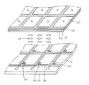
일반적인 액정표시소자의 분해도인 도 1을 참조하여, 액정표시소자의 대략적인 구성에 대하여 살펴보면 다음과 같다.Referring to FIG. 1, which is an exploded view of a general liquid crystal display device, a general configuration of the liquid crystal display device is as follows.
도 1에 도시된 바와 같이, 일반적인 액정표시소자는 일반적으로 상판이라 불리우는 컬러필터 기판(113)과 하판인 박막트랜지스터 어레이 기판(101)과 액정 층(109)으로 구성된다.As shown in FIG. 1, a general liquid crystal display device includes a
상기 컬러필터 기판은, 기판(113) 위에 컬러필터(117), 상기 각 컬러필터(117) 사이에 형성된 블랙매트릭스(BM : black matrix, 115) 및 상기 컬러필터(117)와 블랙매트릭스(115) 위에 형성된 공통전극(111)으로 구성된다.The color filter substrate may include a
상기 박막트랜지스터 어레이 기판(101) 상에는 서로 교차하는 게이트배선(103)과 데이터배선(105)이 형성되어 화소영역(P)이 정의되며, 기 게이트배선(103)과 데이터배선(105)의 교차점에는 박막트랜지스터(TFT)가 형성되어 있다. 상기 화소영역(P)상에는 전술한 바와 같이, 투명한 도전층으로 구성된 화소전극(107)이 형성된다.The
액정층은 상기 상판과 하판 사이에 형성되며, 광굴절률 이방성 성질을 가지는 액정물질(109)로 구성된다.The liquid crystal layer is formed between the upper plate and the lower plate, and is composed of a
그리고, 도 1에 도시되지는 않았지만 액정패널을 제외한 액정표시소자의 나머지 구성요소들을 살펴보면, 상기 액정패널의 양면에는 상판 및 하판에 각각 접촉하여 형성된 편광판이 구비되고, 상기 하판의 편광판 하부에는 램프 및 광학시트로 구성된 백라이트 유닛과 상기 액정패널을 지지하기 위한 탑 케이스 및 보텀 케이스 등이 구비되어 있다.Although not shown in FIG. 1, the remaining components of the liquid crystal display device other than the liquid crystal panel will be described. Both surfaces of the liquid crystal panel may include polarizing plates formed in contact with the upper and lower plates, respectively, under the polarizing plate of the lower plate. A backlight unit composed of an optical sheet, and a top case and a bottom case for supporting the liquid crystal panel are provided.
상기한 액정표시소자를 포함한 대부분의 평판표시장치의 제조방법에 있어서 기판 상에 적층되는 박막물질은 포토리소그래피(photolithography) 공정으로 패터 닝된다.In the manufacturing method of most flat panel display devices including the liquid crystal display device, the thin film material deposited on the substrate is patterned by a photolithography process.
포토리소그래피 공정은 일종의 사진식각공정의 하나이다. 포토리소그래피를 이용하여 패터닝하는 방법은 다음과 같다.The photolithography process is one kind of photolithography process. The patterning method using photolithography is as follows.
먼저 패터닝을 하려 하는 박막 상에 감광물질인 포토레지스트를 도포한 후 , 패턴이 형성된 포토마스크를 정렬하고 노광공정을 진행한다. 이때 사용하는 포토마스크는 투과영역과 차단영역으로 구성되며, 투과영역을 통과한 빛은 포토레지스트를 화학적으로 변화시킨다. 상기 포토레지스트의 화학적 변화는 포토레지스트의 종류에 따라 달라지는 데, 포지티브 포토레지스트는 빛을 받은 부분이 현상액에 의하여 용해되는 성질로 변화되며, 네거티브 포토레지스트는 반대로 빛을 받은 부분이 현성액에 용해되지 않는 성질로 변화된다.(이하 포지티브 포토레지스트를 예로 설명한다.)First, a photoresist as a photosensitive material is applied onto the thin film to be patterned, and then the photomask on which the pattern is formed is aligned and an exposure process is performed. At this time, the photomask used is composed of a transmission region and a blocking region, and light passing through the transmission region chemically changes the photoresist. The chemical change of the photoresist varies depending on the type of photoresist. The positive photoresist is changed to a property in which the lighted part is dissolved by the developer, and the negative photoresist does not dissolve the lighted part in the suspension. (Positive photoresist is exemplified below).
상기 노광공정에 이어서 포토레지스트의 노광된 부분을 현상액을 이용하여 제거하게 되면 박막 상에 포토레지스트 패턴이 형성된다. 상기 포토레지스트 패턴으로 상기 박막을 식각하고, 남픈 포토레지스트 패턴을 제거하면 소정 패턴의 박막이 형성된다.After the exposure process, the exposed portion of the photoresist is removed using a developer to form a photoresist pattern on the thin film. When the thin film is etched with the photoresist pattern and the remaining photoresist pattern is removed, a thin film having a predetermined pattern is formed.
상기 포토리소그래피 공정은 게이트전극 형성, 활성층 패턴 형성, 소스/드레인전극 형성, 콘택트홀 형성 및 화소전극 형성 단계에서 총 3회에서 5회 이용되는 것이 보통이다.The photolithography process is generally used three to five times in the steps of forming a gate electrode, forming an active layer pattern, forming a source / drain electrode, forming a contact hole, and forming a pixel electrode.
그런데 상기에서 살펴본 바와 같이 포토리소그래피 공정에는 고가의 포토마스크가 필요하며, 노광 및 현상과 같은 복잡한 공정이 요구되므로 공정비용이 과다 하고 수율관리가 어려운 문제점이 있다.However, as described above, an expensive photomask is required for the photolithography process, and complicated processes such as exposure and development are required, resulting in excessive process cost and difficulty in yield management.
본 발명은 상기한 문제를 해결하기 위한 것으로, 본 발명에서는 사진식각기술을 대체하여 소프트리소그래피(soft lithography)라는 방법이 사용되며, 본 발명은 상기 소프트리소그래피(soft lithography)에 사용되는 소프트몰드(soft mold)를 만들기 위한 패턴형성용 레지스트와 그 제조방법을 제공하여 소프트 리소그래피에 의한 패턴 형성 방법을 제공하는 데 그 목적이 있다.The present invention is to solve the above problems, in the present invention, a method called soft lithography is used in place of the photolithography technique, the present invention is a soft mold (soft lithography) used in the soft lithography (soft lithography) It is an object of the present invention to provide a pattern forming method by soft lithography by providing a pattern forming resist for manufacturing a mold and a method of manufacturing the same.
삭제delete
상기한 목적을 달성하기 위한 본 발명에 따른 패턴형성용 레지스트는, 친수성 액체 고분자전구체와, 광개시제 및 계면활성제를 포함하는 것을 특징으로 한다.The pattern forming resist according to the present invention for achieving the above object is characterized in that it comprises a hydrophilic liquid polymer precursor, a photoinitiator and a surfactant.
본 발명은 상기 패턴형성용 레지스트를 이용하여 소프트몰드를 제조하는 방법을 포함하며, 본 발명에 따른 소프트몰드 제조방법은, 기판에 제1항에 의한 패턴형성용 레지스트를 도포하는 단계와, 일면에 패턴이 형성된 마스터몰드를 준비하여 상기 패턴형성용 레지스트의 상부에 접촉시키는 단계와, 상기 패턴형성용 레지스트에 광을 조사하여 경화시켜 폴리머로 구성된 소프트몰드를 형성하는 단계 및 상기 소프트몰드를 마스터몰드에서 분리하는 단계를 포함하는 것을 특징으로 한다.The present invention includes a method of manufacturing a soft mold using the pattern forming resist, the soft mold manufacturing method according to the present invention, the step of applying the pattern forming resist according to claim 1 to a substrate, and Preparing a patterned master mold and contacting an upper portion of the pattern forming resist; irradiating and curing the pattern forming resist to light to form a soft mold made of a polymer; and forming the soft mold in the master mold. Characterized in that it comprises a step of separating.
삭제delete
이하 도면을 참조하여 우선 소프트리소그래피에 대해 설명한 다음, 본 발명에 대한 설명을 하기로 한다.Hereinafter, soft lithography will first be described with reference to the drawings, and then the present invention will be described.
도2a 내지 도 2j는 사진식각 공정을 사용하지 않고 패턴을 형성할 수 있는 방법인 소프트리소그라피(soft lithography)를 이용한 액정표시소자의 박막트랜지스터 어레이 기판 제조방법의 일 실시예에 대하여 나타낸 것이다.2A to 2J illustrate an embodiment of a method of manufacturing a thin film transistor array substrate of a liquid crystal display using soft lithography, which is a method of forming a pattern without using a photolithography process.
소프트리소그래피에서는 먼저 도 2a에 도시한 바와 같이, 기판(201) 위에 제박막(203a)을 형성하고 그 위에 액상의 수지 등으로 에치 레지스트(etch resist : 205a)을 형성한다.In soft lithography, first, as shown in FIG. 2A, the
상기 박막(203a)과 에치 레지스트(205a)가 형성된 기판(201)의 이격된 상부로부터 음각(B)과 양각(A)으로 패턴된 소프트몰드(soft mold, 207a)를 상기 에치 레지스트(205a)에 접촉시킨다. 이때, 상기 소프트몰드(207a)는 패턴형성용 레지스트를 경화시켜 만들어진다.A
상기 소프트몰드(207a)는 패턴이 형성될 부분에 대응되도록 위치하며, 상기 양각 패턴(A)을 에치 레지스트(205a)에 접촉한 후 가압하면, 상기 에치 레지스 트(205a)은 액상의 수지이므로 모세관힘과 소프트몰드와 에치레지스트와의 반발력에 의해 상기 소프트몰드(207a)의 음각패턴(B)으로 이동하게 된다.The
따라서, 일정 시간이 경과한 후에 상기 소프트몰드(207a)를 기판과 분리시키면, 도 2b에 도시한 바와 같이 상기 음각패턴(B)의 형상과 동일한 소정 형상의 에치 레지스트(206a) 패턴이 상기 박막(203a) 위에 남게 된다.Accordingly, when the
다음 단계의 공정으로, 도 2c에 도시된 바와 같이. 상기 에치 레지스트(206a) 패턴을 마스크로 하여 박막(203a)을 식각한 후, 에치 레지스트(206a) 패턴을 제거하여, 박막 패턴(203)을 형성한다.In the next step of the process, as shown in Figure 2c. After etching the
전술한 바와 같은, 소프트리소그래피(soft lithography) 공정은 이후 공정에서도 계속 적용되며, 이하에서는 소프트리소그래피(soft lithography)에 대한 자세한 설명은 생략한다.As described above, the soft lithography process continues to be applied to subsequent processes, and detailed description of soft lithography is omitted below.
상기한 바와 같이 소프트리소그래피 공정에는 에치 레지스트와 소프트몰드를 접촉하여 가압하는 에치 레지스트 패턴을 형성하는 단계가 포함되어 있다. 에치 레지스트는 소프트몰드의 패턴 내에 음각에 이동하여 소프트몰드에 형성된 패턴에 대응하는 패턴이 형성되게 된다.
그런데, 에치 레지스트와 소프트몰드의 표면의 반발력이 큰 경우, 즉, 에치 레지스트와 소프트몰드 간의 접착력이 작은 경우에는 에치 레지스트가 소프트몰드의 패턴으로 충분히 이동하지 않아 충분한 패턴의 형성이 어렵게 된다. 이 상태에서 이후 공정을 진행하는 경우 패턴에 불량이 발생할 가능성이 있다.As described above, the soft lithography process includes forming an etch resist pattern for contacting and pressing the etch resist and the soft mold. The etch resist is moved intaglio in the pattern of the soft mold to form a pattern corresponding to the pattern formed on the soft mold.
By the way, when the repelling force of the surface of the etch resist and the soft mold is large, that is, when the adhesion between the etch resist and the soft mold is small, the etch resist does not sufficiently move to the pattern of the soft mold, making it difficult to form a sufficient pattern. If the process is carried out in this state, there is a possibility that a defect occurs in the pattern.
따라서, 소프트몰드와 에치 레지스트간에 접착되면 상기 두 물질간에 컨택(contact)이 양호해지므로 양질의 패턴의 형성이 가능하다.Therefore, when the contact between the soft mold and the etch resist is a good contact (contact) between the two materials it is possible to form a good pattern.
일반적으로 접촉하는 두 물질간의 접착력 및 퍼짐성은 표면에너지에 의존하는데, 소프트몰드의 표면에너지가 클수록 에치 레지스트와 접착력 및 퍼짐성이 좋아진다. 또한 두 물질 간의 접착력은 두 물질의 친수성(hydrophilicity)에 의존하는데, 친수성이 큰 물질일수록 접착력은 커지고, 소수성이 큰 물질일수록 접착력이 작아지는 경향이 있다.In general, the adhesion and spreadability between the two materials in contact depend on the surface energy. The greater the surface energy of the soft mold, the better the adhesion and spreadability of the etch resist. In addition, the adhesion between the two materials depends on the hydrophilicity of the two materials, the higher the hydrophilic material, the greater the adhesion, the more hydrophobic material tends to decrease the adhesion.
본 발명에서는 광경화성 재료를 이용하여 친수성을 띠며 표면에너지가 높은 소프트몰드를 형성하고 이를 이용하여 액정표시소자를 제조하는 방법을 포함한다.The present invention includes a method of forming a soft mold having a hydrophilic property and high surface energy using a photocurable material and manufacturing a liquid crystal display device using the same.
이하 도 3a 내지 도 3e를 참조하여 본 발명에 따른 소프트몰드(soft mold)의 제조방법에 대하여 설명한다.Hereinafter, a method of manufacturing a soft mold according to the present invention will be described with reference to FIGS. 3A to 3E.
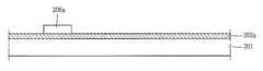
첫 번째 단계의 공정으로 도 3a에 도시된 바와 같이 기판(201 ; back plane)에 소프트몰드를 형성할 재료인 패턴형성용 레지스트(205)를 도포한다.
이때 소프트몰드를 형성할 재료는 패턴을 형성하기 위한 감광성 액체 물질로, 이하 패턴형성용 레지스트라고 한다.In the first step, as shown in FIG. 3A, a pattern forming resist 205, which is a material for forming a soft mold, is applied to a substrate 201 (back plane).
At this time, the material for forming the soft mold is a photosensitive liquid material for forming a pattern, hereinafter referred to as a pattern forming resist.
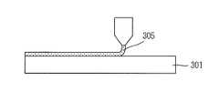
다음 단계의 공정으로 도 3b와 도 3c에 도시된 바와 같이 소프트몰드에 형성하고자 하는 패턴과 대응하는 영역에 소정의 패턴이 형성된 마스터몰드(master mold ; 307)를 준비하여 상기 패턴형성용 레지스트(305)의 상부에 접촉시킨다. 이때 필요한 경우 가압하거나 열을 가하여 패턴형성용 레지스트(305)의 이동성을 증 가시킬 수도 있을 것이다.As a next step, as shown in FIGS. 3B and 3C, a
이때 상기 마스터몰드(307)는 본체와 본체 위에 형성된 소정의 패턴(홈이나 돌출면 등)으로 구성되며, 상기 본체는 유리판이나 유리판 위에 금속이 적층된 것일 수 있다. 그리고 상기 소정의 패턴을 구성하는 물질은 금속, 산화/질화실리콘, 포토레지스트, 왁스 중 어느 하나로 이루어질 수 있다.At this time, the
상기 마스터몰드(307)가 패턴형성용 레지스트(305)와 접촉하게 되면 상기 패턴형성용 레지스트(305)는 액상이므로 도 3c와 같이 상기 마스터몰드(307)의 홈과 돌출면에 대응하여 이동하게 된다.When the
그 다음, 도 3d와 같이, 상기 패턴형성용 레지스트(307)를 소프트몰드로 만들기 위해 경화시키는 과정을 진행한다.
본 발명에 의한 패턴형성용 레지스트(307)는 광이 조사되면 경화되는 물질을 사용한다. 특히 자외선영역의 빛을 사용하여 패턴형성용 레지스트를 경화시키게 되며, 300~500nm의 광을 사용하는 것이 바람직하다.Then, as shown in Figure 3d, the process for curing the pattern forming resist 307 to make a soft mold.
The pattern forming resist 307 according to the present invention uses a material that is cured when light is irradiated. In particular, it is preferable to use a light in the ultraviolet region to cure the resist for pattern formation, and to use a light of 300 ~ 500nm.
마지막으로, 도 3e와 같이, 패턴형성용 레지스트가 경화되어 소프트몰드(305)가 형성되면 마스터몰드(307)를 분리한다.
이때 소프트몰드의 하부의 기판(301)도 분리할 수 있다. 상기 포스트몰드의 하부의 기판(back plane)은 유리 또는 PET(polyethylene terephthalate) 등으로 형성이 가능하다.Finally, as shown in FIG. 3E, when the pattern forming resist is cured to form the
At this time, the
상기한 바와 같이 본 발명에 의한 소프트몰드를 제조하는 방법에서 사용되는 패턴형성 레지스트는 광경화성을 띠는 물질인 것이 바람직하다. 또한 이후 액정표시소자 등을 형성할 때 에치 레지스트와의 접촉성을 좋게 하기 위해 친수성을 가지는 것이 바람직하다.As described above, the patterning resist used in the method for producing a soft mold according to the present invention is preferably a material having photocurability. In addition, when forming a liquid crystal display device or the like, it is preferable to have hydrophilicity in order to improve contact with the etch resist.
이에 따라 본 발명에 의한 소프트몰드의 재료, 즉 패턴형성 레지스트에 대해 이하 설명한다.Accordingly, the material of the soft mold according to the present invention, that is, the pattern forming resist will be described below.
본 발명에 의한 패턴형성 레지스트는 90wt% 이상의 친수성(hydrophilic) 액체 고분자전구체(prepolymer)와, 1~3wt% 정도의 광개시제(photoinitiator) 및 0.01~1wt% 정도의 계면활성제(surfactant)를 포함하며, 마스터몰드 및 광의 조사에 의해 경화되어 성형되는 것을 특징으로 한다.The patterning resist according to the present invention comprises at least 90 wt% of a hydrophilic liquid polymer precursor, a photoinitiator of about 1 to 3 wt%, and a surfactant of about 0.01 to 1 wt%, and a master It is characterized in that it is cured and molded by irradiation of a mold and light.
상기 친수성 액체 고분자전구체는 광경화가 가능한 전구체로서, 바람직하게는 아크릴레이트 전구체(acrylate prepolymer)인 것을 포함한다. 아크릴레이트 전구체로는 HEA(2-hydroxyethyl acrylate), EGDMA(ethyleneglycol dimethacrylate), EGPEA(ethyleneglycol phenyltheracrylate), HPA(hydroxypropyl acrylate), HPPA(hydroxyphenoxypropyl acrylate) 등을 들 수 있으며, 광경화가 가능한고 친수성의 아크릴레이트 전구체를 포함한다.
상기 전구체는 필요에 따라 상기한 전구체 중 어느 한 가지만을 사용할 수도 있으며 두 개 이상의 상기 전구체를 혼합하여 사용하는 것도 가능하다.The hydrophilic liquid polymer precursor is a photocurable precursor, and preferably includes an acrylate precursor. Examples of acrylate precursors include HEA (2-hydroxyethyl acrylate), EGDMA (ethyleneglycol dimethacrylate), EGPEA (ethyleneglycol phenyltheracrylate), HPA (hydroxypropyl acrylate), HPPA (hydroxyphenoxypropyl acrylate), and the like. Precursors.
The precursor may be used only one of the above-described precursors, if necessary, may be used by mixing two or more of the precursors.
상기 광개시제는 빛을 받아 래디컬(radical)을 형성하여 고분자화(polymerization)을 시작시키는 물질로, Irgacure 369, Irgacure 184, Irgacure 819 등의 광경화가 가능한 개시제를 포함한다. 상기 개시제는 상기한 것 중 어느 하나만을 사용할 수 있으며 필요에 따라 복수 가지를 혼합하여 사용하는 것도 가능하다.The photoinitiator is a material that initiates polymerization by receiving radicals to form radicals and includes photocurable initiators such as Irgacure 369, Irgacure 184, and Irgacure 819. The initiator may use only any one of the above, and may be used by mixing a plurality of kinds as necessary.
상기 계면활성제는 표면장력이나 표면에너지를 변화시키기 위해 첨가하는 것 으로 듀퐁(DuPont)사의 FSO-100 등을 사용할 수 있다.The surfactant may be added to change the surface tension or surface energy can be used DuPont's FSO-100 and the like.
본 발명에 의한 상기 패턴형성용 레지스트는 빛을 받아 광개시제에 의해 광반응이 일어나 래디칼이 형성되고 고분자화되어 경화된다. 특히 UV 영역의 광의 조사에 의해 경화되어 성형되는 것을 특징으로 한다. 상기 UV 영역 중 300~500nm의 광을 상기 패턴형성용 레지스트의 경화에 사용할 수 있다.The pattern-forming resist according to the present invention receives light and undergoes photoreaction with a photoinitiator, whereby radicals are formed, polymerized and cured. In particular, it is hardened | cured and shape | molded by irradiation of the light of UV region, It is characterized by the above-mentioned. Light of 300 to 500 nm in the UV region may be used to cure the pattern forming resist.
이상으로 본 발명에 의한 패턴형성용 레지스트와, 패턴형성용 레지스트를 이용하여 소프트몰드를 형성하는 방법 및 상기 소프트몰드를 이용하여 박막의 패턴을 형성하는 방법에 대해 살펴보았다.
상기 설명에서는 박막의 패턴을 형성하는 단계를 나타내었으나 상기 박막 패터닝 단계는 액정표시소자의 게이트전극, 활성층패턴, 소스/드레인전극 및 화소전극 형성 단계, 컬러필터나 블랙매트릭스 형성단계 등에서 사용될 수 있다. 또한 상기 박막의 형성과정은 액정표시소자뿐만 아니라 OLED(Organic Light Emitting Diode)나 기타 평판표시소자를 제조하는 과정에서 사용될 수 있다. 따라서 본 발명은 상기 설명에 국한되지 않으며 다양한 패턴형성 단계에서 사진식각기술과 같은 방법과 함께 사용될 수 있다.The method of forming a soft mold using the pattern forming resist and the pattern forming resist according to the present invention and the method of forming a thin film pattern using the soft mold have been described.
In the above description, a step of forming a thin film pattern is illustrated, but the thin film patterning step may be used in a gate electrode, an active layer pattern, a source / drain electrode and a pixel electrode forming step, a color filter or a black matrix forming step of a liquid crystal display device. In addition, the formation process of the thin film may be used in the process of manufacturing organic light emitting diode (OLED) or other flat panel display devices as well as liquid crystal display devices. Therefore, the present invention is not limited to the above description and can be used with methods such as photolithography in various pattern forming steps.
상기한 설명에 많은 사항이 구체적으로 기재되어 있으나 이것은 발명의 범위를 한정하는 것이라기보다 바람직한 실시예의 예시로서 해석되어야 한다. 따라서 발명은 설명된 실시예에 의하여 정할 것이 아니고 특허청구범위와 특허청구범위에 균등한 것에 의하여 정하여져야 한다.Many details are set forth in the foregoing description but should be construed as illustrative of preferred embodiments rather than to limit the scope of the invention. Therefore, the invention should not be defined by the described embodiments, but should be defined by the claims and their equivalents.
상술한 바와 같이, 본 발명의 액정표시소자의 제조방법에는 소프트 리쏘스라피(soft lithography)가 이용된다. 따라서 사진식각기술을 대체하여 공정비용을 감소시킬 수 있고, 생산수율을 증가시킬 수 있다.As described above, soft lithography is used in the method of manufacturing the liquid crystal display device of the present invention. Therefore, it is possible to reduce the process cost and increase the production yield by replacing the photolithography technique.
또한, 본 발명에 의한 소프트몰드는 친수성을 띠므로 에치 레지스트와 접촉성이 좋아 패턴의 형성시 불량이 감소시킬 수 있는 유리한 효과를 가진다.In addition, since the soft mold according to the present invention has hydrophilicity, the soft mold has a favorable effect of having good contact with the etch resist and reducing defects in forming the pattern.
Claims (12)
Translated fromKoreanPriority Applications (6)
| Application Number | Priority Date | Filing Date | Title |
|---|---|---|---|
| KR1020060059968AKR100832298B1 (en) | 2006-06-29 | 2006-06-29 | Pattern forming resist and soft mold manufacturing method using the same |
| US11/821,161US7838196B2 (en) | 2006-06-29 | 2007-06-22 | Resist for soft mold and method for fabricating liquid crystal display using the same |
| GB0712298AGB2439639B (en) | 2006-06-29 | 2007-06-25 | Resist for soft mould and method for fabricating liquid crystal display using same |
| TW096123249ATWI359328B (en) | 2006-06-29 | 2007-06-27 | A method of fabricating a soft mold and the method |
| JP2007171037AJP4800266B2 (en) | 2006-06-29 | 2007-06-28 | Soft mold and method of manufacturing liquid crystal display device using the same |
| CN2007101268915ACN101097403B (en) | 2006-06-29 | 2007-06-29 | Resist for soft mold and method for fabricating liquid crystal display using the same |
Applications Claiming Priority (1)
| Application Number | Priority Date | Filing Date | Title |
|---|---|---|---|
| KR1020060059968AKR100832298B1 (en) | 2006-06-29 | 2006-06-29 | Pattern forming resist and soft mold manufacturing method using the same |
Publications (2)
| Publication Number | Publication Date |
|---|---|
| KR20080001498A KR20080001498A (en) | 2008-01-03 |
| KR100832298B1true KR100832298B1 (en) | 2008-05-26 |
Family
ID=38352877
Family Applications (1)
| Application Number | Title | Priority Date | Filing Date |
|---|---|---|---|
| KR1020060059968AActiveKR100832298B1 (en) | 2006-06-29 | 2006-06-29 | Pattern forming resist and soft mold manufacturing method using the same |
Country Status (6)
| Country | Link |
|---|---|
| US (1) | US7838196B2 (en) |
| JP (1) | JP4800266B2 (en) |
| KR (1) | KR100832298B1 (en) |
| CN (1) | CN101097403B (en) |
| GB (1) | GB2439639B (en) |
| TW (1) | TWI359328B (en) |
Families Citing this family (10)
| Publication number | Priority date | Publication date | Assignee | Title |
|---|---|---|---|---|
| US7854858B2 (en)* | 2006-12-29 | 2010-12-21 | Lg Display Co., Ltd. | UV curable liquid pre-polymer, and liquid crystal display device using the same and manufacturing method thereof |
| KR101319325B1 (en)* | 2006-12-29 | 2013-10-16 | 엘지디스플레이 주식회사 | Method for Forming Pattern |
| KR20140022890A (en)* | 2011-05-17 | 2014-02-25 | 다이니폰 인사츠 가부시키가이샤 | Three-dimensional display pattern phase difference film and three-dimensional display pattern orientation film master manufacturing method |
| JP6583713B2 (en)* | 2015-04-16 | 2019-10-02 | 大日本印刷株式会社 | Imprint master mold and manufacturing method thereof, imprint film mold and manufacturing method thereof, and manufacturing method of wire grid polarizer |
| CN106802511A (en)* | 2017-04-11 | 2017-06-06 | 京东方科技集团股份有限公司 | A kind of color membrane substrates, its preparation method and relevant apparatus |
| CN108363235B (en)* | 2018-03-02 | 2024-02-09 | 京东方科技集团股份有限公司 | Anti-reflection film and preparation method thereof, array substrate, display device |
| CN109314061A (en)* | 2018-09-11 | 2019-02-05 | 深圳市汇顶科技股份有限公司 | Production method, living things feature recognition mould group and the terminal device of via devices |
| CN113934108B (en)* | 2021-09-06 | 2024-05-03 | 南昌光澜半导体有限公司 | Composite PET soft film and preparation method thereof |
| CN113934109B (en)* | 2021-09-06 | 2024-05-03 | 南昌光澜半导体有限公司 | Composite PET soft film and preparation method thereof |
| CN114815340A (en)* | 2022-05-19 | 2022-07-29 | 豪威半导体(上海)有限责任公司 | LCOS display and manufacturing method thereof |
Citations (2)
| Publication number | Priority date | Publication date | Assignee | Title |
|---|---|---|---|---|
| KR20050120380A (en)* | 2004-06-18 | 2005-12-22 | 엘지.필립스 엘시디 주식회사 | Resist for forming pattern and method for fabricating pattern using the same |
| KR20060045261A (en)* | 2004-11-12 | 2006-05-17 | 엘지.필립스 엘시디 주식회사 | Method and apparatus for manufacturing flat panel display device |
Family Cites Families (34)
| Publication number | Priority date | Publication date | Assignee | Title |
|---|---|---|---|---|
| US4439600A (en)* | 1983-06-03 | 1984-03-27 | Loctite Corporation | Cure to elastomers compositions |
| JPH08203125A (en)* | 1995-01-31 | 1996-08-09 | Pioneer Electron Corp | Laminated optical disk and its production |
| JPH09304757A (en)* | 1996-03-11 | 1997-11-28 | Sharp Corp | Liquid crystal display device and method of manufacturing the same |
| JP2001106765A (en)* | 1999-10-08 | 2001-04-17 | Dainippon Printing Co Ltd | Highly sensitive curable resin, curable resin composition, method for producing them, color filter, and liquid crystal panel |
| JP2004163904A (en) | 2002-09-30 | 2004-06-10 | Rohm & Haas Electronic Materials Llc | Improved photoinitiator |
| KR100870020B1 (en)* | 2002-10-04 | 2008-11-21 | 삼성전자주식회사 | Photosensitive resin composition for controlling dissolution characteristics and pattern formation method of double layer structure using same |
| US20060131784A1 (en)* | 2003-01-10 | 2006-06-22 | Takaki Sugimoto | Flexible mold, method of manufacturing same and method of manufacturing fine structures |
| US7078157B2 (en) | 2003-02-27 | 2006-07-18 | Az Electronic Materials Usa Corp. | Photosensitive composition and use thereof |
| KR100568581B1 (en) | 2003-04-14 | 2006-04-07 | 주식회사 미뉴타텍 | Composition for micropattern forming mold and mold made therefrom |
| KR100911421B1 (en)* | 2003-05-16 | 2009-08-11 | 엘지디스플레이 주식회사 | Color filter forming method using mold and liquid crystal display device manufacturing method including the same |
| JP2007503120A (en)* | 2003-08-19 | 2007-02-15 | ナノオプト コーポレーション | Submicron scale patterning method and system |
| EP3242318A1 (en)* | 2003-12-19 | 2017-11-08 | The University of North Carolina at Chapel Hill | Monodisperse micro-structure or nano-structure product |
| KR101117437B1 (en)* | 2003-12-27 | 2012-02-29 | 엘지디스플레이 주식회사 | Method and Apparatus for Fabricating Flat Panel Display |
| KR101050292B1 (en)* | 2003-12-27 | 2011-07-19 | 엘지디스플레이 주식회사 | Method of manufacturing thin film transistor array substrate |
| KR101010431B1 (en)* | 2003-12-27 | 2011-01-21 | 엘지디스플레이 주식회사 | Method and apparatus for manufacturing flat panel display device |
| KR101076423B1 (en) | 2004-02-06 | 2011-10-25 | 엘지디스플레이 주식회사 | Etch Resist and Method and Apparatus for Fabricating Flat Panel Display Using The Same |
| US7168939B2 (en)* | 2004-02-26 | 2007-01-30 | Hitachi Global Storage Technologies Netherlands Bv | System, method, and apparatus for multilevel UV molding lithography for air bearing surface patterning |
| KR101024650B1 (en)* | 2004-04-13 | 2011-03-25 | 엘지디스플레이 주식회사 | LCD panel and manufacturing method |
| KR101086476B1 (en)* | 2004-04-14 | 2011-11-25 | 엘지디스플레이 주식회사 | LCD panel and manufacturing method |
| JP4696661B2 (en) | 2004-04-26 | 2011-06-08 | 三菱化学株式会社 | Blue composition for color filter, color filter and color image display device |
| KR100641002B1 (en) | 2004-04-30 | 2006-11-02 | 엘지.필립스 엘시디 주식회사 | Liquid crystal display |
| US7401552B2 (en)* | 2004-09-16 | 2008-07-22 | Agfa Graphics N.V. | Method for manufacturing a flexographic printing master |
| US7785504B2 (en)* | 2004-11-11 | 2010-08-31 | Lg Display Co., Ltd. | Thin film patterning apparatus and method of fabricating color filter array substrate using the same |
| GB2436009B (en) | 2004-11-11 | 2008-11-12 | Lg Philips Lcd Co Ltd | Thin Film Patterning Apparatus and Method of Fabricating Color Filter Array Substrate Using the Same |
| KR101137862B1 (en)* | 2005-06-17 | 2012-04-20 | 엘지디스플레이 주식회사 | Fabricating method for flat display device |
| KR101137845B1 (en)* | 2005-06-24 | 2012-04-20 | 엘지디스플레이 주식회사 | method for fabricating soft mold |
| JP4876261B2 (en)* | 2005-10-25 | 2012-02-15 | 国立大学法人北海道大学 | Method for producing patterned material |
| KR101212142B1 (en)* | 2005-11-28 | 2012-12-14 | 엘지디스플레이 주식회사 | Liquid Crystal Display Device And Method For Fabricating The Same |
| KR100705641B1 (en)* | 2006-04-10 | 2007-04-17 | 이화여자대학교 산학협력단 | Mold processing method |
| KR101261606B1 (en)* | 2006-05-09 | 2013-05-09 | 삼성디스플레이 주식회사 | Apparatus for manufacturing a display panel and method for manufacturing the same |
| US7998651B2 (en)* | 2006-05-15 | 2011-08-16 | Asml Netherlands B.V. | Imprint lithography |
| KR100857521B1 (en)* | 2006-06-13 | 2008-09-08 | 엘지디스플레이 주식회사 | Manufacturing method of mold for manufacturing thin film transistor and equipment therefor |
| US20080000373A1 (en)* | 2006-06-30 | 2008-01-03 | Maria Petrucci-Samija | Printing form precursor and process for preparing a stamp from the precursor |
| US7875313B2 (en)* | 2007-04-05 | 2011-01-25 | E. I. Du Pont De Nemours And Company | Method to form a pattern of functional material on a substrate using a mask material |
- 2006
- 2006-06-29KRKR1020060059968Apatent/KR100832298B1/enactiveActive
- 2007
- 2007-06-22USUS11/821,161patent/US7838196B2/enactiveActive
- 2007-06-25GBGB0712298Apatent/GB2439639B/enactiveActive
- 2007-06-27TWTW096123249Apatent/TWI359328B/enactive
- 2007-06-28JPJP2007171037Apatent/JP4800266B2/enactiveActive
- 2007-06-29CNCN2007101268915Apatent/CN101097403B/enactiveActive
Patent Citations (2)
| Publication number | Priority date | Publication date | Assignee | Title |
|---|---|---|---|---|
| KR20050120380A (en)* | 2004-06-18 | 2005-12-22 | 엘지.필립스 엘시디 주식회사 | Resist for forming pattern and method for fabricating pattern using the same |
| KR20060045261A (en)* | 2004-11-12 | 2006-05-17 | 엘지.필립스 엘시디 주식회사 | Method and apparatus for manufacturing flat panel display device |
Also Published As
| Publication number | Publication date |
|---|---|
| GB2439639A (en) | 2008-01-02 |
| CN101097403A (en) | 2008-01-02 |
| US20080003511A1 (en) | 2008-01-03 |
| KR20080001498A (en) | 2008-01-03 |
| GB0712298D0 (en) | 2007-08-01 |
| TWI359328B (en) | 2012-03-01 |
| US7838196B2 (en) | 2010-11-23 |
| JP2008006821A (en) | 2008-01-17 |
| CN101097403B (en) | 2011-04-20 |
| TW200809397A (en) | 2008-02-16 |
| JP4800266B2 (en) | 2011-10-26 |
| GB2439639B (en) | 2009-06-03 |
Similar Documents
| Publication | Publication Date | Title |
|---|---|---|
| KR100832298B1 (en) | Pattern forming resist and soft mold manufacturing method using the same | |
| CN112074784B (en) | Method and apparatus for producing seamless large-area embossing | |
| KR100848559B1 (en) | Soft Mold Manufacturing Method and Pattern Forming Method Using the Same | |
| CN100409034C (en) | Microlens array substrate, method of manufacturing the same, and display | |
| TWI398902B (en) | Soft mold and method of fabricating the same | |
| TWI395026B (en) | Liquid crystal display device and method of fabricating the same | |
| US7361285B2 (en) | Method for fabricating cliche and method for forming pattern using the same | |
| US8291820B2 (en) | Intaglio printing plate, production method for intaglio printing plate, production method for electronic substrate, and production method for display device | |
| JPH11326603A (en) | Microlens array, method of manufacturing the same, and display device | |
| KR20060099885A (en) | Flexible liquid crystal display and its manufacturing method | |
| CN101089731B (en) | Soft mold manufacturing device and method for manufacturing soft mold using the same | |
| KR100675632B1 (en) | Pattern Forming Method and Manufacturing Method of Liquid Crystal Display Using The Same | |
| CN100385267C (en) | Thin film patterning device and method for manufacturing color filter array substrate using same | |
| US6811458B2 (en) | Method for manufacturing liquid crystal display | |
| KR100911421B1 (en) | Color filter forming method using mold and liquid crystal display device manufacturing method including the same | |
| KR20070072181A (en) | Manufacturing method of master mold and master mold and manufacturing method of liquid crystal display device using same | |
| KR20060044263A (en) | Manufacturing Method of Color Filter Array Substrate | |
| CN101192003B (en) | Photocurable organic material and method of fabricating array substrate for liquid crystal display device using the same | |
| KR20080110377A (en) | Etch resist composition and pattern formation method of liquid crystal display device using same | |
| US20070224354A1 (en) | Mold for manufacturing display device and manufacturing method of display device using the same | |
| TWI325080B (en) | ||
| TWI383224B (en) | Manufacturing method of lcd panel and substrate thereof, and lcd apparatus, lcd panel and substrate thereof | |
| KR101117985B1 (en) | Fabricating apparatus for flat display device and method threrby | |
| KR101432574B1 (en) | Liquid crystal display device and manufacturing method thereof | |
| KR20120025731A (en) | In-plane switching mode liquid crystal display device and method of fabricating color filter substrate for in-plane switching mode liquid crystal display device |
Legal Events
| Date | Code | Title | Description |
|---|---|---|---|
| PA0109 | Patent application | Patent event code:PA01091R01D Comment text:Patent Application Patent event date:20060629 | |
| A201 | Request for examination | ||
| PA0201 | Request for examination | Patent event code:PA02012R01D Patent event date:20070321 Comment text:Request for Examination of Application Patent event code:PA02011R01I Patent event date:20060629 Comment text:Patent Application | |
| E902 | Notification of reason for refusal | ||
| PE0902 | Notice of grounds for rejection | Comment text:Notification of reason for refusal Patent event date:20071214 Patent event code:PE09021S01D | |
| PG1501 | Laying open of application | ||
| E701 | Decision to grant or registration of patent right | ||
| PE0701 | Decision of registration | Patent event code:PE07011S01D Comment text:Decision to Grant Registration Patent event date:20080425 | |
| GRNT | Written decision to grant | ||
| PR0701 | Registration of establishment | Comment text:Registration of Establishment Patent event date:20080520 Patent event code:PR07011E01D | |
| PR1002 | Payment of registration fee | Payment date:20080521 End annual number:3 Start annual number:1 | |
| PG1601 | Publication of registration | ||
| PR1001 | Payment of annual fee | Payment date:20110329 Start annual number:4 End annual number:4 | |
| FPAY | Annual fee payment | Payment date:20120330 Year of fee payment:5 | |
| PR1001 | Payment of annual fee | Payment date:20120330 Start annual number:5 End annual number:5 | |
| FPAY | Annual fee payment | Payment date:20130329 Year of fee payment:6 | |
| PR1001 | Payment of annual fee | Payment date:20130329 Start annual number:6 End annual number:6 | |
| FPAY | Annual fee payment | Payment date:20150429 Year of fee payment:8 | |
| PR1001 | Payment of annual fee | Payment date:20150429 Start annual number:8 End annual number:8 | |
| FPAY | Annual fee payment | Payment date:20160428 Year of fee payment:9 | |
| PR1001 | Payment of annual fee | Payment date:20160428 Start annual number:9 End annual number:9 | |
| FPAY | Annual fee payment | Payment date:20170413 Year of fee payment:10 | |
| PR1001 | Payment of annual fee | Payment date:20170413 Start annual number:10 End annual number:10 | |
| FPAY | Annual fee payment | Payment date:20180416 Year of fee payment:11 | |
| PR1001 | Payment of annual fee | Payment date:20180416 Start annual number:11 End annual number:11 | |
| FPAY | Annual fee payment | Payment date:20190417 Year of fee payment:12 | |
| PR1001 | Payment of annual fee | Payment date:20190417 Start annual number:12 End annual number:12 | |
| PR1001 | Payment of annual fee | Payment date:20200422 Start annual number:13 End annual number:13 | |
| PR1001 | Payment of annual fee | Payment date:20210415 Start annual number:14 End annual number:14 | |
| PR1001 | Payment of annual fee | Payment date:20230417 Start annual number:16 End annual number:16 | |
| PR1001 | Payment of annual fee | Payment date:20240415 Start annual number:17 End annual number:17 | |
| PR1001 | Payment of annual fee | Payment date:20250415 Start annual number:18 End annual number:18 |