KR100832021B1 - Semiconductor memory device and driving method thereof - Google Patents
Semiconductor memory device and driving method thereofDownload PDFInfo
- Publication number
- KR100832021B1 KR100832021B1KR1020060059735AKR20060059735AKR100832021B1KR 100832021 B1KR100832021 B1KR 100832021B1KR 1020060059735 AKR1020060059735 AKR 1020060059735AKR 20060059735 AKR20060059735 AKR 20060059735AKR 100832021 B1KR100832021 B1KR 100832021B1
- Authority
- KR
- South Korea
- Prior art keywords
- output
- data
- parameter
- response
- delay
- Prior art date
- Legal status (The legal status is an assumption and is not a legal conclusion. Google has not performed a legal analysis and makes no representation as to the accuracy of the status listed.)
- Active
Links
- 238000000034methodMethods0.000titleclaimsabstractdescription37
- 239000004065semiconductorSubstances0.000titleclaimsabstractdescription16
- 238000005259measurementMethods0.000claimsabstractdescription15
- 230000008569processEffects0.000claimsabstractdescription9
- 230000004044responseEffects0.000claimsdescription44
- 230000003111delayed effectEffects0.000claimsdescription19
- 238000012544monitoring processMethods0.000claimsdescription13
- 238000012360testing methodMethods0.000claimsdescription11
- 230000001360synchronised effectEffects0.000abstractdescription5
- 238000013461designMethods0.000abstractdescription2
- 238000010586diagramMethods0.000description10
- 238000004891communicationMethods0.000description2
- 230000008901benefitEffects0.000description1
- 230000005540biological transmissionEffects0.000description1
- 230000002950deficientEffects0.000description1
- 230000001934delayEffects0.000description1
- 238000011161developmentMethods0.000description1
- 230000000694effectsEffects0.000description1
- 230000006870functionEffects0.000description1
- 230000009467reductionEffects0.000description1
- 238000012795verificationMethods0.000description1
Images


Classifications
- G—PHYSICS
- G11—INFORMATION STORAGE
- G11C—STATIC STORES
- G11C11/00—Digital stores characterised by the use of particular electric or magnetic storage elements; Storage elements therefor
- G11C11/21—Digital stores characterised by the use of particular electric or magnetic storage elements; Storage elements therefor using electric elements
- G11C11/34—Digital stores characterised by the use of particular electric or magnetic storage elements; Storage elements therefor using electric elements using semiconductor devices
- G11C11/40—Digital stores characterised by the use of particular electric or magnetic storage elements; Storage elements therefor using electric elements using semiconductor devices using transistors
- G11C11/401—Digital stores characterised by the use of particular electric or magnetic storage elements; Storage elements therefor using electric elements using semiconductor devices using transistors forming cells needing refreshing or charge regeneration, i.e. dynamic cells
- G11C11/4063—Auxiliary circuits, e.g. for addressing, decoding, driving, writing, sensing or timing
- G11C11/407—Auxiliary circuits, e.g. for addressing, decoding, driving, writing, sensing or timing for memory cells of the field-effect type
- G11C11/4076—Timing circuits
- G—PHYSICS
- G11—INFORMATION STORAGE
- G11C—STATIC STORES
- G11C7/00—Arrangements for writing information into, or reading information out from, a digital store
- G11C7/10—Input/output [I/O] data interface arrangements, e.g. I/O data control circuits, I/O data buffers
- G11C7/1051—Data output circuits, e.g. read-out amplifiers, data output buffers, data output registers, data output level conversion circuits
- G—PHYSICS
- G11—INFORMATION STORAGE
- G11C—STATIC STORES
- G11C11/00—Digital stores characterised by the use of particular electric or magnetic storage elements; Storage elements therefor
- G11C11/21—Digital stores characterised by the use of particular electric or magnetic storage elements; Storage elements therefor using electric elements
- G11C11/34—Digital stores characterised by the use of particular electric or magnetic storage elements; Storage elements therefor using electric elements using semiconductor devices
- G11C11/40—Digital stores characterised by the use of particular electric or magnetic storage elements; Storage elements therefor using electric elements using semiconductor devices using transistors
- G11C11/401—Digital stores characterised by the use of particular electric or magnetic storage elements; Storage elements therefor using electric elements using semiconductor devices using transistors forming cells needing refreshing or charge regeneration, i.e. dynamic cells
- G11C11/4063—Auxiliary circuits, e.g. for addressing, decoding, driving, writing, sensing or timing
- G11C11/407—Auxiliary circuits, e.g. for addressing, decoding, driving, writing, sensing or timing for memory cells of the field-effect type
- G—PHYSICS
- G11—INFORMATION STORAGE
- G11C—STATIC STORES
- G11C29/00—Checking stores for correct operation ; Subsequent repair; Testing stores during standby or offline operation
- G11C29/02—Detection or location of defective auxiliary circuits, e.g. defective refresh counters
- G—PHYSICS
- G11—INFORMATION STORAGE
- G11C—STATIC STORES
- G11C29/00—Checking stores for correct operation ; Subsequent repair; Testing stores during standby or offline operation
- G11C29/02—Detection or location of defective auxiliary circuits, e.g. defective refresh counters
- G11C29/023—Detection or location of defective auxiliary circuits, e.g. defective refresh counters in clock generator or timing circuitry
- G—PHYSICS
- G11—INFORMATION STORAGE
- G11C—STATIC STORES
- G11C29/00—Checking stores for correct operation ; Subsequent repair; Testing stores during standby or offline operation
- G11C29/02—Detection or location of defective auxiliary circuits, e.g. defective refresh counters
- G11C29/028—Detection or location of defective auxiliary circuits, e.g. defective refresh counters with adaption or trimming of parameters
- G—PHYSICS
- G11—INFORMATION STORAGE
- G11C—STATIC STORES
- G11C7/00—Arrangements for writing information into, or reading information out from, a digital store
- G11C7/10—Input/output [I/O] data interface arrangements, e.g. I/O data control circuits, I/O data buffers
- G11C7/1051—Data output circuits, e.g. read-out amplifiers, data output buffers, data output registers, data output level conversion circuits
- G11C7/1069—I/O lines read out arrangements
- G—PHYSICS
- G11—INFORMATION STORAGE
- G11C—STATIC STORES
- G11C7/00—Arrangements for writing information into, or reading information out from, a digital store
- G11C7/22—Read-write [R-W] timing or clocking circuits; Read-write [R-W] control signal generators or management
- G—PHYSICS
- G11—INFORMATION STORAGE
- G11C—STATIC STORES
- G11C7/00—Arrangements for writing information into, or reading information out from, a digital store
- G11C7/22—Read-write [R-W] timing or clocking circuits; Read-write [R-W] control signal generators or management
- G11C7/222—Clock generating, synchronizing or distributing circuits within memory device
- G—PHYSICS
- G11—INFORMATION STORAGE
- G11C—STATIC STORES
- G11C11/00—Digital stores characterised by the use of particular electric or magnetic storage elements; Storage elements therefor
- G11C11/21—Digital stores characterised by the use of particular electric or magnetic storage elements; Storage elements therefor using electric elements
- G11C11/34—Digital stores characterised by the use of particular electric or magnetic storage elements; Storage elements therefor using electric elements using semiconductor devices
- G11C11/40—Digital stores characterised by the use of particular electric or magnetic storage elements; Storage elements therefor using electric elements using semiconductor devices using transistors
- G11C11/401—Digital stores characterised by the use of particular electric or magnetic storage elements; Storage elements therefor using electric elements using semiconductor devices using transistors forming cells needing refreshing or charge regeneration, i.e. dynamic cells
- G—PHYSICS
- G11—INFORMATION STORAGE
- G11C—STATIC STORES
- G11C2207/00—Indexing scheme relating to arrangements for writing information into, or reading information out from, a digital store
- G11C2207/22—Control and timing of internal memory operations
- G11C2207/2254—Calibration
Landscapes
- Engineering & Computer Science (AREA)
- Microelectronics & Electronic Packaging (AREA)
- Computer Hardware Design (AREA)
- Dram (AREA)
Abstract
Translated fromKoreanDescription
Translated fromKorean도 1은 동기식 DRAM과 칩셋의 통신 방식을 나타낸 도면.1 is a diagram illustrating a communication scheme of a synchronous DRAM and a chipset.
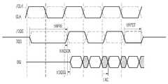
도 2는 DDR SDRAM의 리드시의 AC 파라미터를 나타낸 도면2 is a diagram showing an AC parameter at the time of reading of a DDR SDRAM;
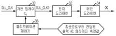
도 3은 본 발명의 제1 실시예에 따른 DRAM의 블럭 다이어그램.3 is a block diagram of a DRAM according to the first embodiment of the present invention;
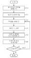
도 4는 본 발명의 제1 실시예에 따른 DRAM의 캘리브레이션 과정을 나타낸 흐름도.4 is a flowchart illustrating a calibration process of a DRAM according to a first embodiment of the present invention.
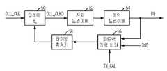
도 5는 본 발명의 제2 실시예에 따른 DRAM의 블럭 다이어그램.5 is a block diagram of a DRAM according to a second embodiment of the present invention;
도 6은 본 발명의 제3 실시예에 따른 DRAM의 블럭 다이어그램.6 is a block diagram of a DRAM according to a third embodiment of the present invention.
* 도면의 주요 부분에 대한 부호의 설명* Explanation of symbols for the main parts of the drawings
30: 가변 딜레이30: variable delay
32: 전치 드라이버32: Pre-driver
34: 메인 드라이버34: main driver
36: 캘리브레이션 제어기36: Calibration Controller
본 발명은 반도체 설계 기술에 관한 것으로, 특히 동기식 반도체 메모리 소자의 출력 AC 파라미터 제어 기술에 관한 것이다.BACKGROUND OF THE INVENTION 1. Field of the Invention The present invention relates to semiconductor design techniques, and more particularly to output AC parameter control techniques for synchronous semiconductor memory devices.
동기식 반도체 메모리 소자는 클럭 발생기에서 생성되는 시스템 클럭을 칩셋(chipset)과 공유하면서 커맨드, 어스레스, 데이터를 그 클럭에 동기화시켜 통신을 수행한다.A synchronous semiconductor memory device communicates by synchronizing a system clock generated by a clock generator with a chipset while synchronizing commands, addresses, and data with the clock.
도 1은 동기식 DRAM과 칩셋의 통신 방식을 나타낸 도면이다.1 is a diagram illustrating a communication method between a synchronous DRAM and a chipset.
도 1을 참조하면, 라이트 동작시 칩셋은 DRAM에 커맨드(CMD), 어드레스(ADD), 데이터(DQ)를 전달하는데, 데이터(DQ)와 함께 데이터 스트로브 신호(DQS)를 DRAM에 보낸다.Referring to FIG. 1, during a write operation, the chipset transmits a command CMD, an address ADD, and data DQ to a DRAM, and sends a data strobe signal DQS to the DRAM along with the data DQ.
한편, 리드 동작시 DRAM은 칩셋으로부터 커맨드(CMD), 어드레스(ADD)를 전달 받고, 그에 대응하는 데이터(DQ)를 데이터 스트로브 신호(DQS)와 함께 칩셋으로 보낸다.In the read operation, the DRAM receives a command CMD and an address ADD from the chipset, and transmits the data DQ corresponding thereto along with the data strobe signal DQS to the chipset.
즉, 라이트시에는 칩셋이 데이터 스트로브 신호(DQS)를 DRAM에 보내고, 리드시에는 DRAM이 데이터 스트로브 신호(DQS)를 칩셋에 보낸다.That is, during writing, the chipset sends the data strobe signal DQS to the DRAM, and at the time of reading, the DRAM sends the data strobe signal DQS to the chipset.
데이터 스트로브 신호(DQS)는 소오스 동기화(source synchronization)를 위한 것으로, 흔히 에코 클럭(echo clock)으로 불리우기도 한다. 데이터 스트로브 신호(DQS)에 맞춰 데이터(DQ)를 스트로빙하면 클럭(CLK)과 데이터(DQ)의 스큐차를 줄 일 수 있다.The data strobe signal (DQS) is for source synchronization and is often referred to as an echo clock. Strobing the data DQ according to the data strobe signal DQS may reduce the skew difference between the clock CLK and the data DQ.
도 2는 DDR SDRAM의 리드시의 AC 파라미터를 나타낸 도면이다.2 is a diagram showing an AC parameter at the time of reading the DDR SDRAM.
도 2를 참조하면 데이터(DQ)와 데이터 스트로브 신호(DQS)의 타이밍을 쉽게 알 수 있다. tDQSQ는 데이터 스트로브 신호(DQS)와 데이터(DQ)의 스큐를 나타내는 파라미터이며, tDQSCK는 데이터 스트로브 신호(DQS)와 클럭(CLK)의 스큐를 나타내는 파라미터이며, tAC는 데이터(DQ)와 클럭(CLK)의 스큐를 나타내는 파라미터이다.Referring to FIG. 2, the timing of the data DQ and the data strobe signal DQS can be easily known. tDQSQ is a parameter representing the skew of the data strobe signal DQS and data DQ, tDQSCK is a parameter representing the skew of the data strobe signal DQS and the clock CLK, and tAC is a parameter representing the data DQ and clock CLK. ) Parameter.
DRAM은 칩셋이 데이터(DQ)를 받아들이는 준비 자세를 취하기 위하여 tRPRE(리드 DQS 프리앰블 시간) 동안 데이터 스트로브 신호(DQS)를 로우-Z(Low-Z) 상태로 만들어 주고, 데이터(DQ) 송신을 완료했을 때에는 tRPST(리드 DQS 포스트앰블 시간) 이후 데이터 스트로브 신호(DQS)를 하이-Z(Hi-Z) 상태로 만들어 주면서 리드 동작을 완료하게 된다.The DRAM puts the data strobe signal (DQS) low-Z during tRPRE (lead DQS preamble time) to prepare the chipset for readiness to accept data (DQ), and allows data (DQ) transmissions. When completed, the read operation is completed by making the data strobe signal DQS high-Z (Hi-Z) after tRPST (lead DQS postamble time).
한편, 앞에서 열거한 AC 파라미터들 중 어느 하나라도 스펙(Spec.)을 벗어나게 되면 칩셋이 데이터(DQ)를 잘못 받아들이게 되어 동작 오류를 유발하게 된다. 그런데, 기존의 DRAM 모듈과 칩셋은 능동적으로 tDQSQ, tDQSCK 등의 출력 AC 파라미터를 조절하는 기능이 없기 때문에 보드 공급 전원의 출렁임(fluctuation)이나 주위 온도 특성 등에 의해 출력 AC 파라미터가 왜곡되는 경우 시스템은 다운될 수밖에 없다. 또한, DRAM의 동작 속도가 빨라질수록 AC 파라미터들의 스펙 만족 구간은 더 작아질 수밖에 없어 고속 DRAM 개발이 점점 더 어려워지고 있다.On the other hand, if any of the AC parameters listed above are out of specification, the chipset will incorrectly accept the data (DQ) and cause an operation error. However, since existing DRAM modules and chipsets do not have a function of actively adjusting output AC parameters such as tDQSQ and tDQSCK, when the output AC parameters are distorted due to fluctuation of the board supply power or ambient temperature characteristics, the system may be down. It must be. In addition, the faster the DRAM operation speed, the smaller the specification satisfying range of the AC parameters becomes, making it difficult to develop high-speed DRAM.
본 발명은 상기와 같은 종래기술의 문제점을 해결하기 위하여 제안된 것으로, 능동적으로 출력 AC 파라미터를 조절할 수 있는 반도체 메모리 소자 및 그 구동방법을 제공하는데 그 목적이 있다.The present invention has been proposed to solve the above problems of the prior art, and an object thereof is to provide a semiconductor memory device capable of actively adjusting the output AC parameter and a driving method thereof.
상기의 기술적 과제를 달성하기 위한 본 발명의 제1 측면에 따르면, 지연고정루프 클럭을 지연시키기 위한 가변 지연 수단; 상기 가변 지연 수단에서 지연 제어된 DLL 클럭에 응답하여 데이터를 출력하기 위한 출력 구동 수단; 및 칩셋으로부터 전달된 출력 AC 파라미터 측정값에 응답하여 상기 가변 지연 수단의 지연시간을 제어하기 위한 캘리브레이션 제어 수단을 구비하는 반도체 메모리 소자가 제공된다.According to a first aspect of the present invention for achieving the above technical problem, variable delay means for delaying the delay locked loop clock; Output driving means for outputting data in response to the DLL clock delayed by the variable delay means; And calibration control means for controlling the delay time of the variable delay means in response to an output AC parameter measurement value transmitted from the chipset.
또한, 본 발명의 제2 측면에 따르면, 지연고정루프 클럭을 지연시키기 위한 가변 지연 수단; 상기 가변 지연 수단에서 지연 제어된 DLL 클럭에 응답하여 데이터를 출력하기 위한 출력 구동 수단; 캘리브레이션 커맨드를 받아 생성된 캘리브레이션 테스트 모드 신호에 응답하여 칩셋으로 전달되는 데이터 및 데이터 스트로브 신호를 피드백 입력하기 위한 피드백 입력 수단; 및 상기 피드백 입력 수단으로부터 출력된 상기 데이터 및 상기 데이터 스트로브 신호를 입력받아 출력 AC 파라미터를 측정하고, 그 측정값에 응답하여 상기 가변 지연 수단의 지연시간을 제어하기 위한 타이밍 측정 수단을 구비하는 반도체 메모리 소자가 제공된다.According to a second aspect of the present invention, there is provided an apparatus, comprising: variable delay means for delaying a delay locked loop clock; Output driving means for outputting data in response to the DLL clock delayed by the variable delay means; Feedback input means for feedback input of data and data strobe signals transmitted to the chipset in response to a calibration test mode signal generated in response to a calibration command; And timing measuring means for receiving the data and the data strobe signal output from the feedback input means to measure an output AC parameter and controlling the delay time of the variable delay means in response to the measured value. An element is provided.
또한, 본 발명의 제3 측면에 따르면, 지연고정루프 클럭을 지연시키기 위한 가변 지연 수단; 상기 가변 지연 수단에서 지연 제어된 DLL 클럭에 응답하여 데이터를 출력하기 위한 출력 구동 수단; 칩셋으로 전달되는 데이터 및 데이터 스트로브 신호를 모니터링하기 위한 실시간 모니터링 수단; 및 상기 실시간 모니터링 수단으로부터 출력된 상기 데이터 및 상기 데이터 스트로브 신호를 입력받아 출력 AC 파라미터를 측정하고, 그 측정값에 응답하여 상기 가변 지연 수단의 지연시간을 제어하기 위한 타이밍 측정 수단을 구비하는 반도체 메모리 소자가 제공된다.According to a third aspect of the present invention, there is provided an apparatus comprising: variable delay means for delaying a delay locked loop clock; Output driving means for outputting data in response to the DLL clock delayed by the variable delay means; Real time monitoring means for monitoring data and data strobe signals delivered to the chipset; And timing measuring means for receiving the data and the data strobe signal outputted from the real time monitoring means, measuring an output AC parameter, and controlling a delay time of the variable delay means in response to the measured value. An element is provided.
또한, 본 발명의 제4 측면에 따르면, 캘리브레이션 커맨드에 응답하여 데이터 스트로브 신호와 데이터를 칩셋으로 전송하는 단계; 상기 데이터 스트로브 신호와 상기 데이터를 이용하여 상기 칩셋에서 측정된 출력 AC 파라미터 측정값을 수신하는 단계; 상기 출력 AC 파라미터 측정값에 응답하여 지연고정루프 클럭에 대한 지연값을 설정하는 단계; 상기 지연고정루프 클럭을 상기 지연값만큼 지연시키는 단계; 및 지연된 상기 지연고정루프 클럭에 응답하여 출력 AC 파라미터가 제어된 데이터 스트로브 신호 및 데이터를 출력하는 단계를 포함하는 반도체 메모리 소자의 구동방법이 제공된다.According to a fourth aspect of the present invention, there is provided a method comprising: transmitting a data strobe signal and data to a chipset in response to a calibration command; Receiving an output AC parameter measurement measured at the chipset using the data strobe signal and the data; Setting a delay value for a delay locked loop clock in response to the output AC parameter measurement; Delaying the delay locked loop clock by the delay value; And outputting a data strobe signal and data whose output AC parameter is controlled in response to the delayed delay locked loop clock.
여기서, 상기 출력 AC 파라미터가 제어된 데이터 스트로브 신호 및 데이터를 출력하는 단계 수행 후, 상기 AC 파라미터가 제어된 데이터 스트로브 신호 및 데이터를 근간으로 상기 칩셋에서 재측정된 출력 AC 파라미터가 스펙에 부합되지 않음에 따라 상기 칩셋에서 측정된 출력 AC 파라미터 측정값을 수신하는 단계로 복귀하는 것이 바람직하다.Here, after performing the step of outputting the data strobe signal and data controlled the output AC parameter, the output AC parameter measured by the chipset based on the data strobe signal and data controlled by the AC parameter does not meet the specification It is preferable to return to the step of receiving the output AC parameter measurement measured in the chipset according to.
또한, 본 발명의 제5 측면에 따르면, 캘리브레이션 커맨드를 받아 캘리브레 이션 테스트 모드 신호를 생성하는 단계; 상기 캘리브레이션 테스트 모드 신호에 응답하여 칩셋으로 전송되는 데이터 스트로브 신호와 데이터를 피드백 입력하는 단계; 피드백 입력된 상기 데이터 스트로브 신호와 상기 데이터를 이용하여 출력 AC 파라미터를 측정하는 단계; 출력 AC 파라미터 측정값에 응답하여 지연고정루프 클럭에 대한 지연값을 설정하는 단계; 상기 지연고정루프 클럭을 상기 지연값만큼 지연시키는 단계; 및 지연된 상기 지연고정루프 클럭에 응답하여 출력 AC 파라미터가 제어된 데이터 스트로브 신호 및 데이터를 출력하는 단계를 포함하는 반도체 메모리 소자의 구동방법이 제공된다.Also, according to a fifth aspect of the present invention, there is provided a method of generating a calibration test mode signal by receiving a calibration command; Feedback inputting data strobe signals and data transmitted to a chipset in response to the calibration test mode signal; Measuring an output AC parameter using the input data strobe signal and the data; Setting a delay value for the delay locked loop clock in response to the output AC parameter measurement; Delaying the delay locked loop clock by the delay value; And outputting a data strobe signal and data whose output AC parameter is controlled in response to the delayed delay locked loop clock.
또한, 본 발명의 제6 측면에 따르면, 칩셋으로 전송되는 데이터 스트로브 신호와 데이터를 실시간 모니터링 하는 단계; 상기 데이터 스트로브 신호와 상기 데이터를 이용하여 출력 AC 파라미터를 측정하는 단계; 출력 AC 파라미터 측정값에 응답하여 지연고정루프 클럭에 대한 지연값을 설정하는 단계; 상기 지연고정루프 클럭을 상기 지연값만큼 지연시키는 단계; 지연된 상기 지연고정루프 클럭에 응답하여 출력 AC 파라미터가 제어된 데이터 스트로브 신호 및 데이터를 출력하는 단계를 포함하는 반도체 메모리 소자의 구동방법이 제공된다.In addition, according to a sixth aspect of the invention, the step of real-time monitoring the data strobe signal and data transmitted to the chipset; Measuring an output AC parameter using the data strobe signal and the data; Setting a delay value for the delay locked loop clock in response to the output AC parameter measurement; Delaying the delay locked loop clock by the delay value; A method of driving a semiconductor memory device, the method comprising: outputting a data strobe signal and data whose output AC parameter is controlled in response to the delayed delay locked loop clock.
본 발명에서는 메모리가 능동적으로 출력 AC 파라미터를 조절하는 타이밍 제어 방식을 제안한다. 첫 번째 방식은 칩셋이 캘리브레이션 커맨드와 출력 AC 파라미터 측정값을 메모리에 전달하고 메모리가 캘리브레이션 과정을 수행하는 것이고, 두 번째 방식은 칩셋이 캘리브레이션 커맨드를 주면 메모리가 출력 AC 파라미터를 측정하여 캘리브레이션 과정을 수행하는 것이고, 세 번째 방식은 칩셋의 캘리브레 이션 커맨드 없이 메모리가 실시간으로 모니터링하면서 데이터 스트로브 신호(DQS)와 데이터(DQ)를 출력하는 것이다.The present invention proposes a timing control scheme in which a memory actively adjusts output AC parameters. In the first method, the chipset passes calibration commands and output AC parameter measurements to the memory, and the memory performs the calibration process. In the second method, the chipset performs a calibration command and the memory measures the output AC parameters to perform the calibration process. The third method is to output the data strobe signal (DQS) and data (DQ) while the memory is monitored in real time without the calibration command of the chipset.
이하, 본 발명이 속한 기술분야에서 통상의 지식을 가진 자가 본 발명을 보다 용이하게 실시할 수 있도록 하기 위하여 본 발명의 바람직한 실시예를 소개하기로 한다.Hereinafter, preferred embodiments of the present invention will be introduced in order to enable those skilled in the art to more easily carry out the present invention.
도 3은 본 발명의 제1 실시예에 따른 DRAM의 블럭 다이어그램이다.3 is a block diagram of a DRAM according to the first embodiment of the present invention.
도 3을 참조하면, 본 실시예에 따른 DRAM은, 지연고정루프(DLL) 클럭(DLL_CLK)을 지연시키기 위한 가변 딜레이(30)와, 가변 딜레이(30)에서 지연 제어된 DLL 클럭(DLL_CLKD)에 응답하여 출력 데이터 신호를 전치 구동하기 위한 전치 드라이버(32)와, 전치 드라이버(32)의 출력신호에 응답하여 데이터 출력단(DQ)을 구동하기 위한 메인 드라이버(34)와, 칩셋으로부터 전달된 출력 AC 파라미터 측정값에 응답하여 가변 딜레이(30)의 지연시간(τd)을 제어하기 위한 캘리브레이션 제어기(36)를 구비한다.Referring to FIG. 3, a DRAM according to the present embodiment includes a
도 4는 본 발명의 제1 실시예에 따른 DRAM의 캘리브레이션 과정을 나타낸 흐름도이다.4 is a flowchart illustrating a calibration process of a DRAM according to a first embodiment of the present invention.
도 4를 참조하면, 우선 칩셋이 캘리브레이션 커맨드를 DRAM에 인가하면(S10), DRAM은 데이터 스트로브 신호(DQS)와 데이터(DQ)를 칩셋으로 보낸다(S12). Referring to FIG. 4, first, when a chipset applies a calibration command to a DRAM (S10), the DRAM sends a data strobe signal DQS and data DQ to the chipset (S12).
이어서, 칩셋은 DRAM으로부터 전달된 데이터 스트로브 신호(DQS)와 데이터(DQ)로 출력 AC 파라미터(예컨대, tDQSCK나 tDQSQ)를 측정하여 그 값을 DRAM에 전달하고(S14), DRAM의 캘리브레이션 제어기(36)가 그 측정값에 응답하여 가변 딜레이(30)의 지연시간(τd)을 설정한다(S16).The chipset then measures the output AC parameters (e.g., tDQSCK or tDQSQ) with the data strobe signal (DQS) and data (DQ) transferred from the DRAM and transfers the values to the DRAM (S14), the DRAM's calibration controller 36 ) Sets the delay time taud of the
이 경우, 가변 딜레이(30)는 DLL 클럭(DLL_CLK)을 +τd 혹은 -τd만큼 지연시키게 되고, 지연된 DLL 클럭(DLL_CLKD)에 의해 전치 드라이버(32)가 구동되어(S18), 결국 AC 파라미터가 제어된 데이터 스트로브 신호(DQS)와 데이터(DQ)가 칩셋에 전달된다(S20).In this case, the
한편, 칩셋은 데이터 스트로브 신호(DQS)와 데이터(DQ)를 근간으로 출력 AC 파라미터를 재측정하여 스펙에 부합되는지를 판단한다(S22). 판단 결과, 스펙에 부합하면 캘리브레이션 과정을 종료하고, 스펙에 부합하지 않으면 다시 그 값을 DRAM에 전달하는 단계(S14)로 돌아가 스펙에 부합할 때까지 루프를 반복한다. 물론, S22 단계 이후는 검증 절차이므로 경우에 따라 이후 단계를 생략할 수 있다.Meanwhile, the chipset re-measures the output AC parameter based on the data strobe signal DQS and the data DQ to determine whether the chip satisfies the specification (S22). As a result of the determination, the calibration process is terminated if the specification is met, and if the specification is not met, the process returns to the step S14 of transferring the value back to the DRAM and the loop is repeated until the specification is met. Of course, since step S22 is a verification procedure, a subsequent step may be omitted in some cases.
도 5는 본 발명의 제2 실시예에 따른 DRAM의 블럭 다이어그램이다.5 is a block diagram of a DRAM according to a second embodiment of the present invention.
도 5를 참조하면, 본 실시예에 따른 DRAM은, 지연고정루프(DLL) 클럭(DLL_CLK)을 지연시키기 위한 가변 딜레이(50)와, 가변 딜레이(50)에서 지연 제어된 DLL 클럭(DLL_CLKD)에 응답하여 출력 데이터 신호를 전치 구동하기 위한 전치 드라이버(52)와, 전치 드라이버(52)의 출력신호에 응답하여 데이터 출력단(DQ)을 구동하기 위한 메인 드라이버(54)와, 캘리브레이션 테스트 모드 신호(TM_CAL)에 응 답하여 데이터(DQ) 및 데이터 스트로브 신호(DQS)를 피드백 입력하기 위한 피드백 입력 버퍼(56)와, 피드백 입력 버퍼(56)로부터 전달된 데이터(DQ)와 데이터 스트로브 신호(DQS)를 입력받아 출력 AC 파라미터(예컨대, tDQSCK나 tDQSQ)를 측정하고, 그 값에 응답하여 가변 딜레이(50)의 지연시간(τd)을 제어하기 위한 타이밍 측정기(58)를 구비한다.Referring to FIG. 5, a DRAM according to the present exemplary embodiment includes a
칩셋으로부터 캘리브레이션 커맨드가 인가되면 DRAM은 이 커맨드를 받아 캘리브레이션 테스트 모드 신호(TM_CAL)를 활성화시킨다. 캘리브레이션 테스트 모드 신호(TM_CAL)가 활성화되면 피드백 입력 버퍼(56)가 인에이블 상태가 되어 데이터(DQ)와 데이터 스트로브 신호(DQS)를 받아들인다. 타이밍 측정기(58)는 데이터(DQ)와 데이터 스트로브 신호(DQS)로 스큐를 측정하여 그 측정값을 기준으로 DLL 클럭(DLL_CLK)에 대한 지연시간(τd)을 제어한다. 이와 같이 DRAM이 캘리브레이션 동작을 수행한 후 캘리브레이션 테스트 모드 신호(TM_CAL)가 비활성화되면 DRAM은 칩셋에 캘리브레이션 테스트 모드 탈출 정보를 전달하여 이후 정상적인 동작을 수행할 수 있도록 한다.When a calibration command is applied from the chipset, the DRAM receives this command to activate the calibration test mode signal TM_CAL. When the calibration test mode signal TM_CAL is activated, the
도 6은 본 발명의 제3 실시예에 따른 DRAM의 블럭 다이어그램이다.6 is a block diagram of a DRAM according to a third embodiment of the present invention.
도 6을 참조하면, 본 실시예에 따른 DRAM은, 지연고정루프(DLL) 클럭(DLL_CLK)을 지연시키기 위한 가변 딜레이(60)와, 가변 딜레이(60)에서 지연 제어된 DLL 클럭(DLL_CLKD)에 응답하여 출력 데이터 신호를 전치 구동하기 위한 전치 드라이버(62)와, 전치 드라이버(52)의 출력신호에 응답하여 데이터 출력단(DQ)을 구동하기 위한 메인 드라이버(64)와, 칩셋으로 전송되는 데이터(DQ) 및 데이터 스트로브 신호(DQS)를 모니터링하기 위한 실시간 모니터링 버퍼(66)와, 실시간 모니터링 버퍼(66)로부터 전달된 데이터(DQ)와 데이터 스트로브 신호(DQS)를 입력받아 출력 AC 파라미터(예컨대, tDQSCK나 tDQSQ)를 측정하고, 그 값에 응답하여 가변 딜레이(60)의 지연시간(τd)을 제어하기 위한 타이밍 측정기(68)를 구비한다.Referring to FIG. 6, a DRAM according to the present embodiment includes a
본 실시예가 전술한 제2 실시예와 달리 칩셋의 캘리브레이션 커맨드 없이 DRAM 자체적으로 캘리브레이션을 수행한다. 출력신호를 모니터링하기 위한 실시간 모니터링 버퍼(66)가 내장되어야 하는 단점이 있지만, DRAM이 칩셋과 통신하면서 캘리브레이션을 수행하는데 소요되는 시간을 생략할 수 있다는 장점이 있다.Unlike the second embodiment described above, the present embodiment performs calibration of the DRAM itself without the calibration command of the chipset. Although there is a disadvantage in that the real-
만일 DRAM 동작 중 어느 순간에 원치 않는 스큐가 발생하게 되면, DRAM이 스큐를 실시간으로 모니터링하고 있기 때문에 시간의 손실 없이 바로 스펙에 부합되도록 스큐를 조절할 수 있다.If an unwanted skew occurs at any moment during DRAM operation, the DRAM monitors the skew in real time, so the skew can be adjusted to meet specifications without losing time.
본 발명의 기술 사상은 상기 바람직한 실시예에 따라 구체적으로 기술되었으나, 상기한 실시예는 그 설명을 위한 것이며 그 제한을 위한 것이 아님을 주의하여야 한다. 또한, 본 발명의 기술 분야의 통상의 전문가라면 본 발명의 기술 사상의 범위 내에서 다양한 실시예가 가능함을 이해할 수 있을 것이다.Although the technical idea of the present invention has been described in detail according to the above preferred embodiment, it should be noted that the above-described embodiment is for the purpose of description and not of limitation. In addition, those skilled in the art will understand that various embodiments are possible within the scope of the technical idea of the present invention.
예컨대, 전술한 실시예에서는 DRAM의 경우를 일례로 들어 설명하였으나, 데이터 스트로브 신호를 사용하여 칩셋과 통신하는 방식을 가진 메모리라면 꼭 DRAM 이 아니어도 본 발명의 적용이 가능하다.For example, in the above-described embodiment, a case of DRAM has been described as an example, but a memory having a method of communicating with a chipset using a data strobe signal may be applicable to the present invention even if the memory is not DRAM.
전술한 본 발명은 메모리가 출력 AC 파라미터를 능동적으로 제어할 수 있도록 함으로써 메모리의 불량률을 낮추고 신뢰도를 향상시키는 효과가 있다. 또한, AC 파라미터들의 스펙 만족 구간의 축소에 대한 대응이 가능하여 고속 메모리 개발에 기여할 수 있다.The present invention described above has the effect of lowering the defective rate of the memory and improving reliability by allowing the memory to actively control the output AC parameters. In addition, it is possible to respond to the reduction of the specification satisfaction interval of the AC parameters can contribute to high-speed memory development.
Claims (10)
Translated fromKoreanPriority Applications (5)
| Application Number | Priority Date | Filing Date | Title |
|---|---|---|---|
| KR1020060059735AKR100832021B1 (en) | 2006-06-29 | 2006-06-29 | Semiconductor memory device and driving method thereof |
| US11/647,402US7489586B2 (en) | 2006-06-29 | 2006-12-29 | Semiconductor memory device and driving method thereof |
| US12/354,158US7746723B2 (en) | 2006-06-29 | 2009-01-15 | Semiconductor memory device and driving method thereof |
| US13/538,130USRE44632E1 (en) | 2006-06-29 | 2012-06-29 | Semiconductor memory device and driving method thereof |
| US14/100,793USRE48341E1 (en) | 2006-06-29 | 2013-12-09 | Semiconductor memory device and driving method thereof |
Applications Claiming Priority (1)
| Application Number | Priority Date | Filing Date | Title |
|---|---|---|---|
| KR1020060059735AKR100832021B1 (en) | 2006-06-29 | 2006-06-29 | Semiconductor memory device and driving method thereof |
Publications (2)
| Publication Number | Publication Date |
|---|---|
| KR20080001339A KR20080001339A (en) | 2008-01-03 |
| KR100832021B1true KR100832021B1 (en) | 2008-05-26 |
Family
ID=38876482
Family Applications (1)
| Application Number | Title | Priority Date | Filing Date |
|---|---|---|---|
| KR1020060059735AActiveKR100832021B1 (en) | 2006-06-29 | 2006-06-29 | Semiconductor memory device and driving method thereof |
Country Status (2)
| Country | Link |
|---|---|
| US (4) | US7489586B2 (en) |
| KR (1) | KR100832021B1 (en) |
Families Citing this family (13)
| Publication number | Priority date | Publication date | Assignee | Title |
|---|---|---|---|---|
| KR100832021B1 (en)* | 2006-06-29 | 2008-05-26 | 주식회사 하이닉스반도체 | Semiconductor memory device and driving method thereof |
| KR100862233B1 (en)* | 2007-01-04 | 2008-10-09 | 한국과학기술원 | Pre-emphasis output circuit with tap delay line with variable delay time |
| US8379459B2 (en) | 2010-07-21 | 2013-02-19 | International Business Machines Corporation | Memory system with delay locked loop (DLL) bypass control |
| KR20130125036A (en)* | 2012-05-08 | 2013-11-18 | 삼성전자주식회사 | System on chip (soc), method of operating the soc, and system having the soc |
| US9304530B1 (en) | 2012-08-28 | 2016-04-05 | Rambus Inc. | Skew-tolerant strobe-to-clock domain crossing |
| KR102298815B1 (en)* | 2015-01-05 | 2021-09-06 | 삼성전자주식회사 | Semiconductor device and semiconductor system |
| US10048357B2 (en) | 2015-06-15 | 2018-08-14 | Microsoft Technology Licensing, Llc | Time-of-flight (TOF) system calibration |
| US9640278B1 (en) | 2015-12-10 | 2017-05-02 | Integrated Device Technology, Inc. | Testability/manufacturing method to adjust output skew timing |
| KR102472123B1 (en)* | 2016-03-16 | 2022-11-30 | 에스케이하이닉스 주식회사 | Semiconductor system and operating method thereof |
| US10115480B1 (en)* | 2017-07-03 | 2018-10-30 | Qualcomm Incorporated | Double data rate synchronous dynamic random access memory (“DDR SDRAM”) data strobe signal calibration |
| KR102273191B1 (en)* | 2017-09-08 | 2021-07-06 | 삼성전자주식회사 | Storage device and data training method thereof |
| KR102493268B1 (en)* | 2021-03-11 | 2023-01-27 | 연세대학교 산학협력단 | Skew Compensation Circuit and method for High Bandwidth Memory |
| KR20240045649A (en)* | 2022-09-30 | 2024-04-08 | 삼성전자주식회사 | Memory device, memory system and method for operating memory system |
Citations (3)
| Publication number | Priority date | Publication date | Assignee | Title |
|---|---|---|---|---|
| KR20050020359A (en)* | 2003-08-22 | 2005-03-04 | 삼성전자주식회사 | Memory device for itself compensating clock skew occurring centering error and clock skew compensating method |
| KR20050048755A (en)* | 2003-11-20 | 2005-05-25 | 주식회사 하이닉스반도체 | Delay locked loop |
| KR20050109813A (en)* | 2004-05-17 | 2005-11-22 | 주식회사 하이닉스반도체 | Memory device having delay locked loop(dll) |
Family Cites Families (13)
| Publication number | Priority date | Publication date | Assignee | Title |
|---|---|---|---|---|
| US6108793A (en)* | 1997-07-18 | 2000-08-22 | Fujitsu Limited | Semiconductor device having timing-stabilization circuit and method of testing such semiconductor device |
| US6489819B1 (en)* | 1998-10-27 | 2002-12-03 | Mitsubishi Denki Kabushiki Kaisha | Clock synchronous semiconductor memory device allowing testing by low speed tester |
| US6646953B1 (en)* | 2000-07-06 | 2003-11-11 | Rambus Inc. | Single-clock, strobeless signaling system |
| US6519188B2 (en)* | 2000-12-18 | 2003-02-11 | Hynix Semiconductor Inc. | Circuit and method for controlling buffers in semiconductor memory device |
| KR100513806B1 (en)* | 2000-12-30 | 2005-09-13 | 주식회사 하이닉스반도체 | Semiconductor Device |
| US6889336B2 (en)* | 2001-01-05 | 2005-05-03 | Micron Technology, Inc. | Apparatus for improving output skew for synchronous integrate circuits has delay circuit for generating unique clock signal by applying programmable delay to delayed clock signal |
| DE10320792B3 (en)* | 2003-04-30 | 2004-10-07 | Infineon Technologies Ag | Arrangement for synchronizing clock signals has phase comparison devices whose output signals control delay time of first delay device, delay time of variable part of second delay device respectively |
| KR100543923B1 (en)* | 2003-08-21 | 2006-01-23 | 주식회사 하이닉스반도체 | Phase Delay Compensation Apparatus and Method in Semiconductor Devices |
| US7171321B2 (en)* | 2004-08-20 | 2007-01-30 | Rambus Inc. | Individual data line strobe-offset control in memory systems |
| US7130226B2 (en)* | 2005-02-09 | 2006-10-31 | Micron Technology, Inc. | Clock generating circuit with multiple modes of operation |
| US8121237B2 (en)* | 2006-03-16 | 2012-02-21 | Rambus Inc. | Signaling system with adaptive timing calibration |
| KR100832021B1 (en)* | 2006-06-29 | 2008-05-26 | 주식회사 하이닉스반도체 | Semiconductor memory device and driving method thereof |
| JP2010122842A (en)* | 2008-11-19 | 2010-06-03 | Nec Electronics Corp | Delay adjustment device, semiconductor device and delay adjustment method |
- 2006
- 2006-06-29KRKR1020060059735Apatent/KR100832021B1/enactiveActive
- 2006-12-29USUS11/647,402patent/US7489586B2/enactiveActive
- 2009
- 2009-01-15USUS12/354,158patent/US7746723B2/ennot_activeCeased
- 2012
- 2012-06-29USUS13/538,130patent/USRE44632E1/enactiveActive
- 2013
- 2013-12-09USUS14/100,793patent/USRE48341E1/enactiveActive
Patent Citations (3)
| Publication number | Priority date | Publication date | Assignee | Title |
|---|---|---|---|---|
| KR20050020359A (en)* | 2003-08-22 | 2005-03-04 | 삼성전자주식회사 | Memory device for itself compensating clock skew occurring centering error and clock skew compensating method |
| KR20050048755A (en)* | 2003-11-20 | 2005-05-25 | 주식회사 하이닉스반도체 | Delay locked loop |
| KR20050109813A (en)* | 2004-05-17 | 2005-11-22 | 주식회사 하이닉스반도체 | Memory device having delay locked loop(dll) |
Also Published As
| Publication number | Publication date |
|---|---|
| US20090122623A1 (en) | 2009-05-14 |
| US7489586B2 (en) | 2009-02-10 |
| US20140098621A1 (en) | 2014-04-10 |
| USRE48341E1 (en) | 2020-12-01 |
| US7746723B2 (en) | 2010-06-29 |
| US20080002514A1 (en) | 2008-01-03 |
| USRE44632E1 (en) | 2013-12-10 |
| KR20080001339A (en) | 2008-01-03 |
Similar Documents
| Publication | Publication Date | Title |
|---|---|---|
| KR100832021B1 (en) | Semiconductor memory device and driving method thereof | |
| US6940768B2 (en) | Programmable data strobe offset with DLL for double data rate (DDR) RAM memory | |
| US8976620B2 (en) | Apparatus and method to adjust clock duty cycle of memory | |
| US10332575B2 (en) | Signal training for prevention of metastability due to clocking indeterminacy | |
| JP6434161B2 (en) | Calibration of control device received from source synchronous interface | |
| KR20100068670A (en) | Interfacing circuit having a channel skew compensating function, communication system including the same, and method of compensating channel skew | |
| US8436641B2 (en) | Circuit and method for generating on-die termination signal and semiconductor apparatus using the same | |
| US10482946B2 (en) | Management of strobe/clock phase tolerances during extended write preambles | |
| US10892032B1 (en) | Write and read common leveling for 4-bit wide DRAMS | |
| CN113223576B (en) | write leveling | |
| CN108009372B (en) | A method of DDR memory virtual write level calibration response | |
| US20190228808A1 (en) | Internal write adjust for a memory device | |
| US8300496B2 (en) | Semiconductor memory apparatus and test method thereof | |
| JP2007134029A (en) | Clock circuit for semiconductor memory | |
| CN113257302B (en) | Write equalization for memory devices | |
| KR20120109958A (en) | Memory device employing command/address calibration | |
| CN106297889B (en) | memory test system and test method thereof | |
| KR100624261B1 (en) | Device and method of data entry | |
| US6452849B1 (en) | Semiconductor device with test mode for performing efficient calibration of measuring apparatus | |
| KR102424896B1 (en) | Data training device and semiconductor device including the same | |
| KR20110130883A (en) | Memory device including write levelization scheme | |
| TWI401695B (en) | Signal adjusting system and signal adjusting method | |
| KR102006239B1 (en) | Data Output Circuit | |
| KR101034036B1 (en) | Semiconductor memory test board, semiconductor memory test system and semiconductor memory test method comprising the same | |
| KR20070069616A (en) | Device test apparatus and method, and its interface apparatus |
Legal Events
| Date | Code | Title | Description |
|---|---|---|---|
| A201 | Request for examination | ||
| PA0109 | Patent application | Patent event code:PA01091R01D Comment text:Patent Application Patent event date:20060629 | |
| PA0201 | Request for examination | ||
| E902 | Notification of reason for refusal | ||
| PE0902 | Notice of grounds for rejection | Comment text:Notification of reason for refusal Patent event date:20070816 Patent event code:PE09021S01D | |
| PG1501 | Laying open of application | ||
| E90F | Notification of reason for final refusal | ||
| PE0902 | Notice of grounds for rejection | Comment text:Final Notice of Reason for Refusal Patent event date:20080108 Patent event code:PE09021S02D | |
| E701 | Decision to grant or registration of patent right | ||
| PE0701 | Decision of registration | Patent event code:PE07011S01D Comment text:Decision to Grant Registration Patent event date:20080429 | |
| GRNT | Written decision to grant | ||
| PR0701 | Registration of establishment | Comment text:Registration of Establishment Patent event date:20080519 Patent event code:PR07011E01D | |
| PR1002 | Payment of registration fee | Payment date:20080520 End annual number:3 Start annual number:1 | |
| PG1601 | Publication of registration | ||
| PR1001 | Payment of annual fee | Payment date:20110429 Start annual number:4 End annual number:4 | |
| PR1001 | Payment of annual fee | Payment date:20120515 Start annual number:5 End annual number:5 | |
| FPAY | Annual fee payment | Payment date:20130513 Year of fee payment:6 | |
| PR1001 | Payment of annual fee | Payment date:20130513 Start annual number:6 End annual number:6 | |
| FPAY | Annual fee payment | Payment date:20140418 Year of fee payment:7 | |
| PR1001 | Payment of annual fee | Payment date:20140418 Start annual number:7 End annual number:7 | |
| FPAY | Annual fee payment | ||
| PR1001 | Payment of annual fee | ||
| FPAY | Annual fee payment | Payment date:20160419 Year of fee payment:9 | |
| PR1001 | Payment of annual fee | Payment date:20160419 Start annual number:9 End annual number:9 | |
| FPAY | Annual fee payment | Payment date:20170420 Year of fee payment:10 | |
| PR1001 | Payment of annual fee | Payment date:20170420 Start annual number:10 End annual number:10 | |
| FPAY | Annual fee payment | Payment date:20180417 Year of fee payment:11 | |
| PR1001 | Payment of annual fee | Payment date:20180417 Start annual number:11 End annual number:11 | |
| FPAY | Annual fee payment | Payment date:20190417 Year of fee payment:12 | |
| PR1001 | Payment of annual fee | Payment date:20190417 Start annual number:12 End annual number:12 | |
| PR1001 | Payment of annual fee | Payment date:20200417 Start annual number:13 End annual number:13 | |
| PR1001 | Payment of annual fee | Payment date:20230418 Start annual number:16 End annual number:16 | |
| PR1001 | Payment of annual fee | Payment date:20240402 Start annual number:17 End annual number:17 |