KR100831436B1 - Cvd method - Google Patents
Cvd methodDownload PDFInfo
- Publication number
- KR100831436B1 KR100831436B1KR1020010011430AKR20010011430AKR100831436B1KR 100831436 B1KR100831436 B1KR 100831436B1KR 1020010011430 AKR1020010011430 AKR 1020010011430AKR 20010011430 AKR20010011430 AKR 20010011430AKR 100831436 B1KR100831436 B1KR 100831436B1
- Authority
- KR
- South Korea
- Prior art keywords
- film
- gas
- forming
- chamber
- supplying
- Prior art date
- Legal status (The legal status is an assumption and is not a legal conclusion. Google has not performed a legal analysis and makes no representation as to the accuracy of the status listed.)
- Expired - Lifetime
Links
- 238000000034methodMethods0.000titleclaimsabstractdescription50
- 238000002161passivationMethods0.000claimsabstractdescription80
- 238000005229chemical vapour depositionMethods0.000claimsdescription34
- 238000012545processingMethods0.000claimsdescription34
- 229910052731fluorineInorganic materials0.000claimsdescription24
- 238000004140cleaningMethods0.000claimsdescription22
- YCKRFDGAMUMZLT-UHFFFAOYSA-NFluorine atomChemical compound[F]YCKRFDGAMUMZLT-UHFFFAOYSA-N0.000claimsdescription21
- 239000011737fluorineSubstances0.000claimsdescription21
- 229910052719titaniumInorganic materials0.000claimsdescription17
- 229910001512metal fluorideInorganic materials0.000claimsdescription14
- 238000000151depositionMethods0.000claimsdescription10
- 230000008021depositionEffects0.000claimsdescription10
- 239000000126substanceSubstances0.000claimsdescription10
- 229910052751metalInorganic materials0.000claimsdescription9
- 239000002184metalSubstances0.000claimsdescription9
- 229910052759nickelInorganic materials0.000claimsdescription9
- 238000005498polishingMethods0.000claimsdescription8
- 229910000990Ni alloyInorganic materials0.000claimsdescription6
- 229910001510metal chlorideInorganic materials0.000claimsdescription6
- 229910045601alloyInorganic materials0.000claimsdescription4
- 239000000956alloySubstances0.000claimsdescription4
- 239000011248coating agentSubstances0.000claimsdescription4
- 238000000576coating methodMethods0.000claimsdescription4
- 229910052804chromiumInorganic materials0.000claimsdescription3
- 229910010293ceramic materialInorganic materials0.000claimsdescription2
- 229910052742ironInorganic materials0.000claimsdescription2
- 150000002902organometallic compoundsChemical class0.000claimsdescription2
- 229910052709silverInorganic materials0.000claimsdescription2
- RTAQQCXQSZGOHL-UHFFFAOYSA-NTitaniumChemical compound[Ti]RTAQQCXQSZGOHL-UHFFFAOYSA-N0.000claims14
- 239000010936titaniumSubstances0.000claims14
- PXHVJJICTQNCMI-UHFFFAOYSA-NnickelSubstances[Ni]PXHVJJICTQNCMI-UHFFFAOYSA-N0.000claims11
- 238000010438heat treatmentMethods0.000claims4
- 239000007769metal materialSubstances0.000claims2
- 238000003754machiningMethods0.000claims1
- 230000015572biosynthetic processEffects0.000abstractdescription11
- 239000012528membraneSubstances0.000abstractdescription2
- 238000000926separation methodMethods0.000abstractdescription2
- 239000010408filmSubstances0.000description114
- 239000007789gasSubstances0.000description99
- 239000010409thin filmSubstances0.000description13
- 235000012431wafersNutrition0.000description13
- 239000004065semiconductorSubstances0.000description11
- 239000000463materialSubstances0.000description8
- KRHYYFGTRYWZRS-UHFFFAOYSA-MFluoride anionChemical compound[F-]KRHYYFGTRYWZRS-UHFFFAOYSA-M0.000description7
- 238000012360testing methodMethods0.000description6
- 238000005259measurementMethods0.000description5
- 239000002244precipitateSubstances0.000description5
- 229910001000nickel titaniumInorganic materials0.000description4
- VEXZGXHMUGYJMC-UHFFFAOYSA-MChloride anionChemical compound[Cl-]VEXZGXHMUGYJMC-UHFFFAOYSA-M0.000description3
- 101100258315Neurospora crassa (strain ATCC 24698 / 74-OR23-1A / CBS 708.71 / DSM 1257 / FGSC 987) crc-1 geneProteins0.000description3
- PWHVEHULNLETOV-UHFFFAOYSA-NNic-1Natural productsC12OC2C2(O)CC=CC(=O)C2(C)C(CCC2=C3)C1C2=CC=C3C(C)C1OC(O)C2(C)OC2(C)C1PWHVEHULNLETOV-UHFFFAOYSA-N0.000description3
- 229910052782aluminiumInorganic materials0.000description3
- 150000001875compoundsChemical class0.000description3
- 230000000694effectsEffects0.000description3
- 238000005240physical vapour depositionMethods0.000description3
- 238000002441X-ray diffractionMethods0.000description2
- 230000002411adverseEffects0.000description2
- 239000007795chemical reaction productSubstances0.000description2
- 229910052802copperInorganic materials0.000description2
- 230000007797corrosionEffects0.000description2
- 238000005260corrosionMethods0.000description2
- 238000004519manufacturing processMethods0.000description2
- 239000011159matrix materialSubstances0.000description2
- 150000002736metal compoundsChemical class0.000description2
- 150000002739metalsChemical class0.000description2
- 238000010926purgeMethods0.000description2
- 239000000758substrateSubstances0.000description2
- OKTJSMMVPCPJKN-UHFFFAOYSA-NCarbonChemical compound[C]OKTJSMMVPCPJKN-UHFFFAOYSA-N0.000description1
- 229910003902SiCl 4Inorganic materials0.000description1
- 229910004337Ti-NiInorganic materials0.000description1
- 229910008484TiSiInorganic materials0.000description1
- ATJFFYVFTNAWJD-UHFFFAOYSA-NTinChemical compound[Sn]ATJFFYVFTNAWJD-UHFFFAOYSA-N0.000description1
- 229910011209Ti—NiInorganic materials0.000description1
- -1WSiChemical class0.000description1
- 238000005275alloyingMethods0.000description1
- PNEYBMLMFCGWSK-UHFFFAOYSA-Naluminium oxideInorganic materials[O-2].[O-2].[O-2].[Al+3].[Al+3]PNEYBMLMFCGWSK-UHFFFAOYSA-N0.000description1
- 238000004458analytical methodMethods0.000description1
- 230000004888barrier functionEffects0.000description1
- 229910052799carbonInorganic materials0.000description1
- 239000012159carrier gasSubstances0.000description1
- 238000005137deposition processMethods0.000description1
- 238000013461designMethods0.000description1
- 230000006866deteriorationEffects0.000description1
- 239000006185dispersionSubstances0.000description1
- 229910000856hastalloyInorganic materials0.000description1
- KHYBPSFKEHXSLX-UHFFFAOYSA-NiminotitaniumChemical compound[Ti]=NKHYBPSFKEHXSLX-UHFFFAOYSA-N0.000description1
- 238000011065in-situ storageMethods0.000description1
- 238000009413insulationMethods0.000description1
- 230000010354integrationEffects0.000description1
- 238000011835investigationMethods0.000description1
- 238000012986modificationMethods0.000description1
- 230000004048modificationEffects0.000description1
- 238000007747platingMethods0.000description1
- 238000004544sputter depositionMethods0.000description1
- 239000003381stabilizerSubstances0.000description1
Images


Classifications
- C—CHEMISTRY; METALLURGY
- C23—COATING METALLIC MATERIAL; COATING MATERIAL WITH METALLIC MATERIAL; CHEMICAL SURFACE TREATMENT; DIFFUSION TREATMENT OF METALLIC MATERIAL; COATING BY VACUUM EVAPORATION, BY SPUTTERING, BY ION IMPLANTATION OR BY CHEMICAL VAPOUR DEPOSITION, IN GENERAL; INHIBITING CORROSION OF METALLIC MATERIAL OR INCRUSTATION IN GENERAL
- C23C—COATING METALLIC MATERIAL; COATING MATERIAL WITH METALLIC MATERIAL; SURFACE TREATMENT OF METALLIC MATERIAL BY DIFFUSION INTO THE SURFACE, BY CHEMICAL CONVERSION OR SUBSTITUTION; COATING BY VACUUM EVAPORATION, BY SPUTTERING, BY ION IMPLANTATION OR BY CHEMICAL VAPOUR DEPOSITION, IN GENERAL
- C23C16/00—Chemical coating by decomposition of gaseous compounds, without leaving reaction products of surface material in the coating, i.e. chemical vapour deposition [CVD] processes
- C23C16/44—Chemical coating by decomposition of gaseous compounds, without leaving reaction products of surface material in the coating, i.e. chemical vapour deposition [CVD] processes characterised by the method of coating
- C23C16/4401—Means for minimising impurities, e.g. dust, moisture or residual gas, in the reaction chamber
- C23C16/4404—Coatings or surface treatment on the inside of the reaction chamber or on parts thereof
- C—CHEMISTRY; METALLURGY
- C23—COATING METALLIC MATERIAL; COATING MATERIAL WITH METALLIC MATERIAL; CHEMICAL SURFACE TREATMENT; DIFFUSION TREATMENT OF METALLIC MATERIAL; COATING BY VACUUM EVAPORATION, BY SPUTTERING, BY ION IMPLANTATION OR BY CHEMICAL VAPOUR DEPOSITION, IN GENERAL; INHIBITING CORROSION OF METALLIC MATERIAL OR INCRUSTATION IN GENERAL
- C23C—COATING METALLIC MATERIAL; COATING MATERIAL WITH METALLIC MATERIAL; SURFACE TREATMENT OF METALLIC MATERIAL BY DIFFUSION INTO THE SURFACE, BY CHEMICAL CONVERSION OR SUBSTITUTION; COATING BY VACUUM EVAPORATION, BY SPUTTERING, BY ION IMPLANTATION OR BY CHEMICAL VAPOUR DEPOSITION, IN GENERAL
- C23C16/00—Chemical coating by decomposition of gaseous compounds, without leaving reaction products of surface material in the coating, i.e. chemical vapour deposition [CVD] processes
- C23C16/44—Chemical coating by decomposition of gaseous compounds, without leaving reaction products of surface material in the coating, i.e. chemical vapour deposition [CVD] processes characterised by the method of coating
- C23C16/455—Chemical coating by decomposition of gaseous compounds, without leaving reaction products of surface material in the coating, i.e. chemical vapour deposition [CVD] processes characterised by the method of coating characterised by the method used for introducing gases into reaction chamber or for modifying gas flows in reaction chamber
- C23C16/45563—Gas nozzles
- C23C16/45565—Shower nozzles
Landscapes
- Chemical & Material Sciences (AREA)
- General Chemical & Material Sciences (AREA)
- Chemical Kinetics & Catalysis (AREA)
- Engineering & Computer Science (AREA)
- Materials Engineering (AREA)
- Mechanical Engineering (AREA)
- Metallurgy (AREA)
- Organic Chemistry (AREA)
- Chemical Vapour Deposition (AREA)
- Electrodes Of Semiconductors (AREA)
Abstract
Translated fromKoreanDescription
Translated fromKorean도 1은, 본 발명의 실시에 사용되는 CVD 성막장치의 일례를 나타내는 단면도,1 is a cross-sectional view showing an example of a CVD film deposition apparatus used in the practice of the present invention;
도 2는, TiCl4 및 ClF3처리의 싸이클시험시에 있어서의 NC-Ni 샘플표면의 EDAX 측정 프로파일을 나타내는 챠트,Fig. 2 is a chart showing the EDAX measurement profile of the NC-Ni sample surface during the cycle test of TiCl4 and ClF3 treatment;
도 3은, TiCl4 및 ClF3처리의 싸이클시험시에 있어서의 C22 샘플표면의 EDAX 측정 프로파일을 나타내는 챠트,3 is a chart showing an EDAX measurement profile of a C22 sample surface during a cycle test of TiCl4 and ClF3 treatment;
도 4는, TiCl4 및 ClF3처리에 관계하는 염화물 및 불화물의 깁스(Gibbs)의 자유에너지를 나타내는 그래프,4 is a graph showing the free energy of Gibbs of chloride and fluoride related to TiCl4 and ClF3 treatment,
도 5는, TiCl4 및 ClF3처리의 싸이클시험에 있어서, 각 처리시에서의 NC-Ni 샘플의 표면상태를 모식적으로 나타내는 단면도,5 is a cross-sectional view schematically showing the surface state of an NC-Ni sample in each treatment in a cycle test of TiCl4 and ClF3 treatment;
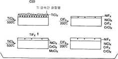
도 6은, TiCl4 및 ClF3처리의 싸이클시험에 있어서, 각 처리시에서의 C22샘플의 표면상태를 모식적으로 나타내는 단면도,6 is a cross-sectional view schematically showing the surface state of a C22 sample in each treatment in a cycle test of TiCl4 and ClF3 treatment;
도 7은, 본 발명의 1실시형태에 관한 CVD 성막처리의 공정을 설명하기 위한 플로우 챠트이다.7 is a flowchart for explaining a step of the CVD film forming process according to the embodiment of the present invention.
<도면의 주요부분에 대한 부호의 설명><Description of the symbols for the main parts of the drawings>
11 : 챔버11a : 천장벽11
11b : 바닥벽12 : 서셉터11b: bottom wall 12: susceptor
13 : 지지부재14 : 히터13
15 : 히터16 : 가이드링15
19 : 절연부재20 : 샤워헤드19: insulation member 20: shower head
20a : 상단블록체20b : 중단블록체20a:
20c : 하단블록체21 : 제 1 도입구20c: lower block 21 21: first inlet
22 : 제 2 도입구23, 25 : TiCl4 통로22: second inlet 23, 25: TiCl4 passage
24, 26 : H2 통로27, 28 : TiCl4 토출구멍24, 26: H2 passage 27, 28: TiCl4 discharge hole
31 : TiCl4원 32, 34, 36, 38 : 배관31: TiCl4
33 : ClF3원 35 : Ar 원33: ClF3 Circle 35: Ar Circle
37 : H2원 39 : 밸브37: H2 circle 39: valve
40 : 질량유량 제어기 41 : 전환밸브40: mass flow controller 41: switching valve
42 : 정합기43 : 고주파전원42: matching device 43: high frequency power supply
44 : 배기관45 : 배기장치44
W : 반도체웨이퍼
W: Semiconductor Wafer
본 발명은, 챔버내에 성막가스를 공급하여 피처리체에 성막처리를 실시하는 화학적 증착 성막방법에 관한 것이다.BACKGROUND OF THE
반도체제조공정에 있어서는, 피처리체인 반도체 웨이퍼(이하, 단순히 "웨이퍼"라 기재함)에 형성된 배선사이의 홀내의 박막을 매설하기 위해서, 혹은 그 박막이 배리어층으로서 기능하도록 하기 위하여, Ti, Al 또는 Cu 등의 금속이나, WSi, TiN 또는 TiSi 등의 금속화합물을 퇴적시켜 박막을 형성하고 있다.In the semiconductor manufacturing process, in order to embed a thin film in a hole between wirings formed in a semiconductor wafer (hereinafter simply referred to as "wafer") which is an object to be processed, or to make the thin film function as a barrier layer, Ti, Al Alternatively, metals such as Cu and metal compounds such as WSi, TiN, or TiSi are deposited to form a thin film.
종래, 이들 금속이나 금속화합물의 박막은 물리적 증착(PVD)을 사용하여 성막되었다. 최근에는 디바이스가 미세화 및 고집적화가 특히 요구되어, 디자인 룰이 특히 엄격하게 되어 있고, 매립성이 나쁜 PVD에서는 충분한 특성을 얻는다는 것이 곤란하게 되었다. 따라서, 이러한 박막을 보다 양질의 막을 형성할 것을 기대할 수 있는 화학적 증착(CVD)으로 성막하는 것이 행하여지고 있다.Conventionally, thin films of these metals and metal compounds have been formed using physical vapor deposition (PVD). In recent years, miniaturization and high integration of devices are particularly required, and design rules are particularly strict, and it is difficult to obtain sufficient characteristics in PVDs with poor embedding properties. Therefore, the film is formed by chemical vapor deposition (CVD) which can be expected to form a higher quality film.
예컨대, Ti 박막을 CVD 로 성막할 때에는, 성막가스로서 예컨대 TiCl4가 사용되고, 환원가스로서 예컨대 H2가 사용되며, 플라즈마 안정제로서 Ar 이 사용된다. 그리고, 이와 같은 가스를 사용하여, 최초에 프리코트처리를 행하고, 이어서, 본 성막처리를 행한다. 그리고, 이와 같은 성막처리후, 정기적으로 또는 필요에 따라 예컨대 ClF3가스에 의해 크리닝을 한다.
For example, when forming a Ti thin film by CVD, for example, TiCl4 is used as the film forming gas, H2 is used as the reducing gas, and Ar is used as the plasma stabilizer. Then, using such a gas, the precoat process is first performed, and then the film forming process is performed. Then, after such a film forming treatment, cleaning is performed periodically or as necessary, for example, by ClF3 gas.
그러나, 이러한 Ti 박막의 성막에 있어서는, 프리코트시에, 예컨대 챔버내에 배치된 가스공급용의 샤워헤드의 표면에 막이 벗겨지는 현상이 발생한다는 문제가 있다. 이러한 문제는 샤워헤드의 표면과 가스공급샤워헤드상에 형성된 박막 사이의 나쁜 고착성에 관련된 것으로 생각된다. 이러한 문제는 샤워헤드에만 일어나는 것은 아니며, 동일한 문제가 챔버내의 다른 부재에도 발생될 가능성이 있다. 또한, 다른 재료의 CVD 성막처리시에도 생길 가능성이 있다.However, in the film formation of such a Ti thin film, there is a problem that a film peels off on the surface of a shower head for gas supply disposed in a chamber, for example, during precoat. This problem is thought to be related to the poor adhesion between the surface of the showerhead and the thin film formed on the gas supply showerhead. This problem does not only occur in the showerhead, but the same problem is likely to occur in other members in the chamber. In addition, there is a possibility that it also occurs during the CVD film-forming of other materials.
본 발명은 상술한 문제점을 해결하하며, 챔버내벽 및/또는 챔버내부재의 막박리를 저비용으로 효과적으로 방지할 수 있는 화학적 증착 성막방법을 제공하는 것을 목적으로 한다.
It is an object of the present invention to solve the above-mentioned problems and to provide a chemical vapor deposition method which can effectively prevent film separation of a chamber inner wall and / or a chamber inner member at low cost.
본 발명자등은, 이러한 프리코트시의 막의 박리에 대하여 조사한 결과, 이러한 박리는 장치내에 신품인 상태에서, 또는 화학세정(화학연마) 등의 처리가 실시된 샤워헤드가 도입되었을 때에 생긴다는 것, 및 한번 ClF3가스에 의해 크리닝된 후에는 발생하지 않는다는 것을 확인하였다. 이 사실을 기초로 더욱 검토한 결과, 챔버내에 소정의 가스를 공급함으로써 챔버내벽 및/또는 챔버내부재표면에 패시베이션(passivation)막을 형성할 수 있게 되고, 이 패시베이션막에 의해 프리코트시에 벗겨지기 쉬운 막의 형성을 방지할 수가 있는 것을 발견하였다. 예컨대, 불소함유가스 등을 공급하여 미리 챔버내벽 및/또는 챔버내 부재표면에 예컨대 금속불화물이나 금속염화물의 패시베이션막을 형성시켜 놓음으로써, 프리코트시에 쉽게 벗겨지지 않는 강고한 막이나 기체의 불화물이 형성되어, 쉽게 벗겨지는 막이 형성되지 않는다.The inventors have investigated such peeling of the film at the time of precoating, and it is found that such peeling occurs when a shower head subjected to a treatment such as chemical cleaning (chemical polishing) or the like is introduced in a new state in the apparatus, And once cleaned by ClF3 gas, it did not occur. As a result of further investigation on the basis of this fact, a passivation film can be formed on the inner wall of the chamber and / or the surface of the inner member of the chamber by supplying a predetermined gas into the chamber, and the passivation film is peeled off during the precoat. It was found that the formation of an easy film can be prevented. For example, by supplying a fluorine-containing gas or the like to form a passivation film of, for example, metal fluoride or metal chloride on the inner wall of the chamber and / or the surface of the member in the chamber, a rigid film or gas fluoride that is not easily peeled off during precoating Formed, no film is easily peeled off.
본 발명은 이러한 지견에 따라서 행해진 것으로서, 본 발명의 제 1 실시형태에 따르면, 화학적 증착 성막처리를 실시하는 챔버내에, 피처리체를 존재시키지 않은 상태로, 패시베이션용가스를 공급하고, 챔버내 벽 및 챔버내 부재표면에 패시베이션막을 형성하는 공정과; 계속해서 상기 챔버안에, 피처리체를 존재시키지 않은 상태로, 프리코트용가스를 공급하여, 상기 패시베이션막의 표면에 프리코트막을 형성하는 공정과; 상기 챔버안에 피처리체를 장입하는 공정; 및, 상기 챔버안에 성막용가스를 공급하여, 피처리체에 대하여 성막처리를 하는 공정을 구비하는 것을 특징으로 하는 화학적증착 성막방법을 제공한다.The present invention has been made in accordance with the above findings. According to the first embodiment of the present invention, a gas for passivation is supplied in a chamber in which a chemical vapor deposition process is performed without a target object, and a wall in the chamber and Forming a passivation film on the surface of the member in the chamber; Subsequently supplying a precoat gas to form a precoat film on the surface of the passivation film in a state in which the object to be processed is not present in the chamber; Charging an object to be processed into the chamber; And supplying a film forming gas into the chamber to perform a film forming process on the object to be treated.
본 발명의 제 2 실시형태에 따르면, 화학적증착 성막처리를 실시하는 챔버내에, 피처리체를 존재시키지 않은 상태로, 패시베이션용가스를 공급하여, 챔버안벽 및 챔버내 부재표면에 패시베이션막을 형성하는 공정; 계속해서 상기 챔버내에, 피처리체를 존재시키지 않은 상태로, 프리코트용가스를 공급하고, 또한 제 1 플라즈마를 생성하고, 상기 패시베이션막의 표면에 프리코트막을 형성하는 공정과; 상기 챔버내에 피처리체를 장입하는 공정; 및, 상기 챔버내에 성막용가스를 공급하고, 또한 제 2 플라즈마를 생성하여, 피처리체에 대하여 성막처리를 하는 공정을 구비하는 것을 특징으로 하는 화학적증착 성막방법을 제공한다.According to a second aspect of the present invention, there is provided a process for forming a passivation film on a chamber inner wall and an inner surface of a chamber by supplying a gas for passivation in a chamber in which a chemical vapor deposition process is performed, without a target object being present; Subsequently supplying a precoat gas, generating a first plasma, and forming a precoat film on the surface of the passivation film in a state in which the object to be processed is not present in the chamber; Charging an object to be processed into the chamber; And a step of supplying a film forming gas into the chamber, generating a second plasma, and performing a film forming process on the object to be treated.
본 발명의 제 3 실시형태에 따르면, 화학적 증착 성막처리를 실시하는 챔버안에, 피처리체를 존재시키지 않은 상태로, 불소함유가스를 공급하여, 챔버내벽 및 챔버내 부재표면에 미리 금속불화물의 패시베이션막을 형성하는 공정; 이어서 상기 챔버안에, 피처리체를 존재시키지 않은 상태로, 성막용가스를 공급하여 패시베이션막의 표면에 프리코트막을 형성하는 공정과; 상기 챔버내에 피처리체를 장입하는 공정; 및, 상기 챔버안에 성막용가스를 공급하여 피처리체에 대하여 성막처리를 하는 공정을 구비하는 것을 특징으로 하는 화학적 증착 성막방법을 제공한다.According to the third embodiment of the present invention, a fluorine-containing gas is supplied in a chamber in which a chemical vapor deposition process is performed without a target object to be present, and a passivation film of a metal fluoride is formed in advance on the inner wall of the chamber and the member surface in the chamber. Forming step; A process of forming a precoat film on the surface of the passivation film by supplying a film forming gas in the chamber without a target object present in the chamber; Charging an object to be processed into the chamber; And supplying a film forming gas into the chamber to perform a film forming process on the object to be treated.
본 발명의 제 4 실시형태에 따르면, 화학적 증착 성막처리를 실시하는 챔버안에, 피처리체를 존재시키지 않은 상태로, 불소함유가스를 공급하여, 챔버내벽 및 챔버내 부재표면에 미리 금속불화물의 패시베이션막을 형성하는 공정과; 이어서 상기 챔버안에, 피처리체를 존재시키지 않은 상태로, 성막용가스를 공급하고, 또한 제 1 플라즈마를 생성하여 패시베이션막의 표면에 프리코트막을 형성하는 공정과; 상기 챔버내에 피처리체를 장입하는 공정과; 상기 챔버내에 성막용가스를 공급하고, 또한 제 2 플라즈마를 생성하여 피처리체에 대하여 성막처리를 하는 공정을 구비하는 것을 특징으로 하는 화학적 증착 성막방법을 제공한다.According to the fourth embodiment of the present invention, a fluorine-containing gas is supplied in a chamber in which a chemical vapor deposition process is performed without a target object to be present, and a passivation film of metal fluoride is formed in advance on the inner wall of the chamber and the member surface in the chamber. Forming step; Then supplying a film forming gas, and generating a first plasma to form a precoat film on the surface of the passivation film in the chamber without a target object present; Charging an object to be processed into the chamber; And a step of supplying a film forming gas into the chamber, and generating a second plasma to perform a film forming process on the object to be treated.
본 발명의 제 5 실시형태에 따르면, 화학적 증착 성막처리를 실시하는 챔버와, 상기 챔버내에 성막가스를 공급하는 성막가스공급계 및 상기 챔버내에 성막후 의 크리닝을 하는 크리닝가스로서 불소함유가스를 공급하는 크리닝가스공급계를 구비하는 화학적 증착 처리장치를 사용하는 성막처리 방법에 있어서, 상기 챔버내에, 피처리체를 존재시키지 않은 상태로, 상기 크리닝가스인 불소함유가스를 공급하고, 상기 챔버내벽 및 챔버내부재에 금속불화물의 패시베이션막을 형성하는 공정과; 이어서, 상기 챔버내에, 피처리체를 존재시키지 않은 상태로, 상기 성막가스공급계에서 성막용가스를 공급하여 패시베이션막의 표면에 프리코트막을 형성하는 공정과; 상기 챔버내에 피처리체를 장입하는 공정; 및, 상기 챔버내에 성막가스공급계에서 성막가스를 공급하여 피처리체에 대하여 성막처리를 하는 공정을 구비하는 것을 특징으로 하는 화학적 증착 성막방법을 제공한다.According to the fifth embodiment of the present invention, a fluorine-containing gas is supplied as a chamber for performing chemical vapor deposition, a film forming gas supply system for supplying film forming gas into the chamber, and a cleaning gas for cleaning after film formation in the chamber. A film forming method using a chemical vapor deposition processing apparatus having a cleaning gas supply system, wherein the fluorine-containing gas, which is the cleaning gas, is supplied to the chamber without a target object being present, and the chamber inner wall and chamber Forming a passivation film of metal fluoride in the inner material; Then forming a precoat film on the surface of the passivation film by supplying the film forming gas from the film forming gas supply system in a state in which the object to be processed is not present in the chamber; Charging an object to be processed into the chamber; And supplying the deposition gas from the deposition gas supply system into the chamber to perform the deposition process on the object to be treated.
본 발명에 의하면, 피처리체가 존재하지 않은 상태의 챔버내에 패시베이션용가스를 도입한다는 간단한 방법으로 챔버내벽 및 챔버내 부재표면에 프리코트시에 막박리를 발생시키지 않는 소정의 패시베이션막을 형성할 수 있다. 따라서, 챔버내벽 및/또는 챔버내부재의 막박리를 저비용이며 효율적으로 방지할 수가 있다.According to the present invention, it is possible to form a predetermined passivation film on the inner wall of the chamber and the surface of the member inside the chamber that does not cause film peeling during precoat by a simple method of introducing the passivation gas into the chamber in the absence of the workpiece. . Therefore, film peeling of the chamber inner wall and / or the chamber inner member can be prevented at low cost and efficiently.
예컨대, 본 발명의 제3 및 제4 실시형태에서와 같이, 챔버내에 불소함유가스를 공급함으로써 챔버내벽 및/또는 챔버내 부재표면에 불화물의 패시베이션막을 형성하는 경우에는, 이 불화물의 패시베이션막은, 가령 그 후에 공급된 성막가스와의 사이에서 반응이 생겼다고 해도 반응생성물을 기체성분으로서 배출하는 것이 가능하며, 막박리를 효율적으로 방지하여 벗겨진 막에 의한 처리 때문에 일어나는 악영향을 방지할 수가 있다.For example, as in the third and fourth embodiments of the present invention, when the fluoride passivation film is formed on the inner wall of the chamber and / or on the member surface within the chamber by supplying the fluorine-containing gas into the chamber, the passivation film of the fluoride is, for example, Thereafter, even if a reaction occurs between the supplied film forming gases, the reaction product can be discharged as a gas component, and the film is effectively prevented from being removed, thereby preventing the adverse effects caused by the treatment with the peeled film.
또한, 본 발명의 제5 실시형태에서와 같이, CVD 성막장치가, 크리닝가스로서 불소함유가스, 예컨대 ClF3를 공급하는 크리닝가스공급계를 구비하는 경우에는, 패시베이션막을 형성할 때에, 원래 CVD 성막장치에 설치되는 크리닝가스공급계에서 미리 크리닝가스를 소정온도의 챔버내에 도입하면 되므로, 지극히 용이하게 챔버내벽 및/또는 챔버내부재표면에 패시베이션막을 형성할 수가 있다.In addition, as in the fifth embodiment of the present invention, when the CVD film forming apparatus includes a cleaning gas supply system for supplying a fluorine-containing gas such as ClF3 as the cleaning gas, the original CVD film is formed when the passivation film is formed. Since the cleaning gas is introduced into the chamber at a predetermined temperature in advance in the cleaning gas supply system installed in the apparatus, it is possible to form a passivation film on the chamber inner wall and / or the surface of the chamber member.
(실시예)(Example)
이하, 본 발명의 실시예에 관해서 구체적으로 설명한다.EMBODIMENT OF THE INVENTION Hereinafter, the Example of this invention is described concretely.
우선, 본 발명에 이른 경위에 대하여, CVD 에 의한 Ti 박막의 성막처리를 예를 들어 설명한다. 도 1은, CVD 성막장치의 일예를 나타내는 단면도이다. 이 성막장치는, 기밀하게 구성된 대략 원통형상의 챔버(11)를 가지고 있으며, 그 중에는 피처리체인 반도체 웨이퍼(W)를 수평으로 지지하기 위한 서셉터(12)가 원통형의 지지부재(13)에 의해 지지된 상태에서 배치되어 있다. 서셉터(12)의 바깥 가장자리부에는 반도체 웨이퍼를 가이드하기 위한 가이드링(16)이 설치되어 있다. 또한, 서셉터(12)에는 히터(14)가 매립되어 있고, 이 히터(14)는 전원(15)으로부터 급전됨으로써 피처리체인 반도체 웨이퍼(W)를 소정의 온도로 가열한다.First, the film forming process of the Ti thin film by CVD will be described with reference to the process according to the present invention. 1 is a cross-sectional view showing an example of a CVD film deposition apparatus. This film forming apparatus has a substantially
챔버(11)의 천장벽(11a)에는, 절연부재(19)를 통해 샤워헤드(20)가 설치되어 있다. 이 샤워헤드(20)는, 상단블록체(20a), 중단블록체(20b), 하단블록체(20c)로 구성되어 있고, 상단블록(20a)의 윗면에는, TiCl4를 도입하기 위한 제 1 도입구(21)와, 환원가스로서의 H2를 도입하기 위한 제 2 도입구(22)가 형성되어 있다. 상단블록체(20a) 내에서는, 제 1 도입구(21)에서 다수의 TiCl4통로(23)가 분기하고 있고, TiCl4통로(23)가 중단블록체(20b)에 형성된 TiCl4통로(25)에 연통하고 있으며, 또한 하단블록체(20c)의 TiCl4토출구멍(27)에 연통하고 있다. 또한, 상단블록체(20a) 안에서는, 제 2 도입구(22)에서 다수의 H2통로(24)가 분기하고 있고, H2통로(24)가 중단블록체(20b)에 형성된 H2통로(26)에 연통하고 있으며, 또한 하단블록체(20c)의 H2토출구멍(28)에 연통하고 있다. 즉, 샤워헤드(20)는, TiCl4과 H2가 완전히 독립하여 챔버(11)내에 공급되는 매트릭스타입의 샤워헤드이고, 이들은 토출후에 혼합되어 반응이 생긴다.The
상기 제 1 도입구(21)에는 TiCl4원(31)으로부터 연장되는 배관(32)이 접속되어 있고, 배관(32)에는 캐리어가스인 Ar원(35)으로부터 연장되는 배관(36)이 접속되어 있고, TiCl4원(31)으로부터의 TiCl4가스가 배관(36)을 지나서 공급된 Ar가스에 캐리어되어 배관(32)을 통해 챔버(11)내에 공급된다. 또한, 배관(32)에는 크리닝가스인 ClF3를 공급하는 ClF3원(33)으로부터 연장되는 배관(34)이 접속되어 있고, 배관(34) 및 배관(32)을 통해 챔버(11)내에 ClF3가스를 공급하는 것이 가능해지고 있다. 상기 제 2 도입구에는 H2원(37)으로부터 뻗어나가는 배관(38)이 접속되어 있고, H2원(37)으로부터의 H2가스가 배관(38)을 통해 챔버(11)내에 공급된다. 또, 각 가스원으로부터의 배관(32,34,36,38)에는, 어느 것이나 밸브(39) 및 질량유량 제어기(40)가 설치되어 있다. 또한, 배관(34)에는 배관(32)의 접속부분근방에 전환밸 브(41)가 설치되어 있다. 또, 도시하지는 않지만, 챔버(11)내에 N2가스를 공급하는 라인도 설치되어 있다.A
샤워헤드(20)에는, 정합기(42)를 통해 고주파전원(43)이 접속되어 있고, 이 고주파전원(43)으로부터 샤워헤드(20)에 고주파전력이 공급됨으로써, 샤워헤드(20)를 통해 챔버(11)내에 공급된 가스가 플라즈마화되어, 이에 따라 성막반응이 진행된다.The high
챔버(11)의 바닥벽(11b)에는, 배기관(44)이 접속되어 있고, 이 배기관(44)에는 배기장치(45)가 접속되어 있다. 그리고 이 배기장치(45)를 작동시킴으로써, 챔버(11)내를 소정의 진공도까지 감압하는 것이 가능해지고 있다.An
이러한 장치에 의해 반도체웨이퍼(W)에 Ti 박막을 성막하기 위해서는, 일반적으로, 우선, 히터(14)에 의해 챔버(11)내를 소정온도에 가열하면서 배기장치(45)에 의해 챔버(11)내를 계속 배기하여, TiCl4 가스와 Ar 가스 및 H2가스를 소정의 유량비로 챔버 (11)내에 도입하고, 챔버(11)내를 소정의 압력으로 함으로써, 고주파전원(43)으로부터 샤워헤드(20)에 고주파전력을 공급하여 챔버(11)내에 플라즈마를 생성시키고, 챔버(11)의 내벽이나 챔버(11)내에 배치되어 있는 샤워헤드(20) 등의 챔버내부재의 표면에 프리코트처리를 한다.In order to form a Ti thin film on the semiconductor wafer W by such an apparatus, generally, first, the
그 후, 챔버내에 반도체웨이퍼(W)를 장입하고, 히터(14)에 의해 웨이퍼를 소정온도로 가열하고, 프리코트와 같은 조건의 가스를 공급하여, Ti 박막의 성막처리를 소정시간 행한다. 이 때의 Ti 박막의 성막처리는, 예컨대 400 내지 1000℃ 정 도의 온도로 행한다.Thereafter, the semiconductor wafer W is charged into the chamber, the
일정한 수의 반도체웨이퍼 W 가 성막후, 챔버(11)로부터 반출되고, 챔버(11)내에 크리닝가스인 ClF3가스가 도입되어 챔버(11)내가 크리닝된다.After a certain number of semiconductor wafers W are formed, they are carried out from the
이러한 장치에 있어서는, 샤워헤드(20)의 상단블록체(20a), 중단블록체(20b)로서 Ni계 합금(헤스텔로이C22), 하단블록(20c)으로서 순Ni[노멀카본(NC)-Ni]를 사용하고 있다. 이러한 샤워헤드로서 신품의 것, 또는 표면을 화학세정(화학연마), 기계연마, 가공성형한 것, 또한 성막으로 사용한 표면을 가공성형한 것을 사용한 경우에는, 프리코트중에 샤워헤드의 표면「하단블록(20c)의 아래면」에서 막박리가 발생한다는 문제가 생겼다.In such a device, pure Ni (normal carbon (NC) -Ni) as the Ni-based alloy (Hestelloy C22) and the
이러한 막박리의 원인을 조사하기 위해서 샤워헤드의 재료인 상술한 NC-Ni 및 C22에 관해서 부식시험을 행하였다. 또, Ti-CVD 프로세스에 있어서 부식성가스는 TiCl4가스 및 ClF3가스이므로, 여기서는 TiCl4가스 및 ClF3가스에 의한 부식시험을 교대로 2회씩 행하였다.In order to investigate the cause of such a film peeling, the corrosion test was done about the above-mentioned NC-Ni and C22 which are materials of a showerhead. In the Ti-CVD process, since the corrosive gas is a TiCl4 gas and a ClF3 gas, the corrosion test by the TiCl4 gas and the ClF3 gas was alternately performed twice.
실험조건은 이하와 같다.Experimental conditions are as follows.
(1)TiCl4(1) TiCl4
Ar 유량 : 0.090 m3/sec (1500 sccm)Ar flow rate: 0.090 m3 / sec (1500 sccm)
TiCl4유량 : 0.003 m3/sec (50 sccm)TiCl4 flow rate: 0.003 m3 / sec (50 sccm)
압력 : 733.2 Pa (5.5 Torr)Pressure: 733.2 Pa (5.5 Torr)
시간 : 400 minTime: 400 min
온도 : 500℃ (히터설정온도)Temperature: 500 ℃ (heater set temperature)
(2)ClF3(2) ClF3
Ar 유량 : 0.030 m3/sec (500 sccm)Ar flow rate: 0.030 m3 / sec (500 sccm)
TiCl4유량 : 0.003 m3/sec (50 sccm)TiCl4 flow rate: 0.003 m3 / sec (50 sccm)
압력 : 173.3 Pa (1.3 Torr)Pressure: 173.3 Pa (1.3 Torr)
시간 : 62 minTime: 62 min
온도 : 200℃(히터설정온도)Temperature: 200 ℃ (heater set temperature)
표면상태를 SEM 관찰하였다. 그 결과, NC-Ni의 경우, 최초의 TiCl4처리에 의해서, 표면에 결정형상의 석출물이 관찰되었다. 다음 ClF3처리에 의해 표면상태는 악화하지만, 2번째의 TiCl4처리후는 석출물은 관찰되지 않았다. 한편, C22의 경우, 최초의 TiCl4처리에 의해서, NC-Ni의 경우와 같은 결정형상석출물이 관찰되었다. 다음 ClF3처리에 의해, Ni 와 같은 표면상태의 악화는 보이지 않지만, 대신에 표면에 박막형상의 물질이 균열되어 있는 상태가 확인되었다. 2회째의 TiCl4처리후는 석출물은 잔존하고 있었지만 막박리는 관찰되지 않았다.The surface state was observed by SEM. As a result, in the case of NC-Ni, crystalline precipitates were observed on the surface by the first TiCl4 treatment. The surface state deteriorated by the next ClF3 treatment, but no precipitate was observed after the second TiCl4 treatment. On the other hand, in the case of C22, the same crystalline precipitates as in the case of NC-Ni were observed by the first TiCl4 treatment. By the next ClF3 treatment, the deterioration of the surface state such as Ni was not observed, but the state in which the thin film-like substance was cracked on the surface was confirmed instead. After the second TiCl4 treatment, precipitates remained but no film peeling was observed.
다음에, 각 처리기의 샘플에 관해서 EDAX (Energy-Dispersion Analysis of X-ray)측정을 행하였다. 그 측정 프로파일을 도 2 및 도 3에 나타낸다.Next, EDAX (Energy-Dispersion Analysis of X-ray) measurement was performed about the sample of each processor. The measurement profile is shown in FIG. 2 and FIG.
도 2는 Ni에 관해서의 결과이지만, 최초의 TiCl4처리후의 샘플로서는 Ni의 그 외에 Ti와 Cl가 검출되었다. 다음 ClF3처리후의 샘플로서는 Ti는 검출되지 않고, 2회째의 TiCl4처리후에 있어서도 Ti는 검출되지 않았다. 즉, ClF3처리에 의해 Ti가 완전히 제거되고, 2회째의 TiCl4처리에서는 Ti는 석출하지 않았다.Figure 2 but the results with regard to Ni, as the handle4 after the first TiCl samples were detected in addition to the Ti and Cl in the Ni. Ti was not detected as a sample after the next ClF3 treatment, and Ti was not detected even after the second TiCl4 treatment. That is, Ti was completely removed by ClF3 treatment, and Ti was not precipitated in the second TiCl4 treatment.
한편, 도 3은 C22의 결과인데, 최초의 TiCl4처리후의 샘플로서는 Ni 및 합금원소 외에도 Ti가 검출되었다. 그러나, 도 2 에서나타낸 NC-Ni 의 경우와 마찬가지로, 다음 ClF3처리후의 샘플로서는 Ti는 검출되지 않고, 2회째의 TiCl4처리후에 있어서도 Ti는 검출되지 않았다.On the other hand, Fig. 3 shows the result of C22. As the sample after the first TiCl4 treatment, Ti was detected in addition to Ni and alloying elements. However, as in the case of NC-Ni shown in FIG. 2, Ti was not detected as a sample after the next ClF3 treatment, and Ti was not detected even after the second TiCl4 treatment.
다음에, 각 처리후의 샘플에 관해서 XRD(X-ray diffraction) 측정을 하였다. 그 결과, NC-Ni에서는, 최초의 TiCl4처리후의 샘플로서는 NiTi가 확인되고, 다음 ClF3처리에 의해 NiTi는 확인되지 않고 NiF3가 확인되었다. 한편, C22에서는, 어떤 처리후에도 면심립방정(面心立方晶)(fcc)합금만이 확인되었다.Next, XRD (X-ray diffraction) measurements were performed on the samples after each treatment. As a result, in Ti-Ni, NiTi was confirmed as the sample after the first TiCl4 treatment, and NiTi was not confirmed by the next ClF3 treatment, but NiF3 was confirmed. On the other hand, in C22, only the surface core grain boundary (fcc) alloy was confirmed after any treatment.
이들 반응계에서 생성될 가능성이 있는 염화물 및 불화물의 깁스의 자유에너지에 있어서는 도 4에 나타낸 바와 같이, 500℃에 있어서,As for the free energy of the cast of chloride and fluoride which may be produced by these reaction systems, as shown in FIG. 4, at 500 degreeC,
ΔG(TiClx)<ΔG(CrC12), ΔG(NiC12)ΔG (TiClx ) <ΔG (CrC12 ), ΔG (NiC12 )
ΔG (TiFx)<ΔG (CrFx)ΔG (TiFx ) <ΔG (CrFx )
이며, Cl분위기하에서는, Cr, Ni보다도 Ti가 염화되기 쉽고, TiClx가 석출하 는 경향이 있다. 마찬가지로 F 분위기하에서도 Ti가 불화되는 쪽에 평형이 기운다. 그러나, TiFx는 증기압이 높기 때문에, 기화하고 석출하지 않는다.In the Cl atmosphere, Ti is more easily chlorided than Cr and Ni, and TiClx tends to precipitate. Similarly, in the F atmosphere, the equilibrium tends to be on the side where Ti is fluorinated. However, since TiFx has a high vapor pressure, it does not vaporize and precipitate.
이상의 결과로부터, 1회째의 TiCl4처리, ClF3처리, 2회째의 TiCl4처리에 관해서 이하의 반응식이 발생한다고 생각된다.From the above results, it is believed that the following reaction formula occurs with respect to the TiCl4 treatment, ClF3 process, TiCl4 the second process of the first time.
(1)순수 Ni (NC-Ni)(1) Pure Ni (NC-Ni)
(1회째의 TiCl4처리)(First TiCl4 Treatment)
Ni + TiCl4→NiTi + NiClx↑+ TiClx↑Ni + TiCl4 → NiTi + NiClx ↑ + TiClx ↑
(ClF3처리)(ClF3 treatment)
NiTi + TiClx+ ClF3 →TiFx↑+ NiFx(PF)+Cl2↑NiTi + TiClx + ClF3 → TiFx ↑ + NiFx (PF) + Cl2 ↑
(2회째의 TiCl4처리)(TiCl4 treatment of the second time)
NiFx + TiCl4→NiC1x↑+ TiFx↑NiFx + TiCl4 → NiC1x ↑ + TiFx ↑
(2)헤스텔로이(C22)(2) Hastelloy (C22)
(1회째의 TiCl4처리 )(The first TiCl4 treatment)
Ni + Cr + TiCl4→ NiC1x↑+ CrC1x(PF) + TiClx↑Ni + Cr + TiCl4 → NiC1x ↑ + CrC1x (PF) + TiClx ↑
(ClF3처리)(ClF3 treatment)
Ni+ CrClx+ ClF3→ NiFx(PF) + CrFx↑+ Cl3↑Ni + CrClx + ClF3 → NiFx (PF) + CrFx ↑ + Cl3 ↑
(2회째의 TiCl4처리)(TiCl4 treatment of the second time)
NiFx+ Cr + TiCl4→ NiClx↑ + CrC1x(PF) + TiFx↑NiFx + Cr + TiCl4 → NiClx ↑ + CrC1x (PF) + TiFx ↑
(이상의 식중, PF는 패시베이션필름을 나타낸다.)(In the above formula, PF represents a passivation film.)
이러한 반응이 생기고 있는 상태를 도 5 및 도 6에 모식적으로 나타낸다. 도 5는 NC-Ni의 경우, 도 6는 C22의 경우 이다. 이와 같이 NC-Ni의 경우 및 C22의 경우 어느 것이나, 최초에 TiCl4처리를 한 경우에는 표면에 박리되기 쉬운 TiClx가 형성되지만, ClF3처리를 함으로써, TiClx는 형성되지 않고 NiFx 패시베이션막이 형성된다. 그리고, 그 후에 다시 TiCl4처리를 했을 때에는, 이 NiFx패시베이션막이 형성되어 있으므로, TiClx 의 박리되기기 쉬운 막은 생성되지 않고, 기체형상의 NiClx나 TiFx, CrFx패시베이션막 등이 생기기 때문에, 막박리는 쉽게 생기지 않는다.5 and 6 schematically show a state in which such a reaction occurs. 5 is a case of NC-Ni, Figure 6 is a case of C22. This would, as each case of the case, and C22 of the NC-Ni, the case where the TiCl4 treatment initially, but forming an easy TiClx is peeled off the surface, by the ClF3 process, TiClx is not formed NiFx passivation film Is formed. When the TiCl4 treatment is performed again later, since the NiFx passivation film is formed, a film that is easily peeled off of TiClx is not formed, and thus a gaseous NiClx , TiFx , CrFx passivation film, or the like is formed. , The peeling does not occur easily.
이상, 본 발명에서는, 예컨대 도 1의 CVD-Ti 성막장치를 사용하여 CVD-Ti 박막을 성막함에 있어서, 예컨대 샤워헤드(20)로서 신품의 것 또는 화학세정된 것이 도입된 경우에, 최초에 챔버(11)내에 ClF3원(33)으로부터 ClF3가스를 도입하고, 현장에서 샤워헤드(20)의 표면에 NiFx패시베이션막을 형성한다(STEP1). 그 후, ClF3가스의 공급을 멈추고, TiCl4원(31)으로부터 TiCl4를 챔버(11)내에 도입하면서, 고주파전원(43)으로부터 샤워헤드(20)에 고주파전력을 인가하여 챔버(11)에 도입한 가스를 플라즈마화시켜, 프리코트막을 형성한다(STEP2). 그 후 챔버내에 반도체웨 이퍼(W)를 장입하고(STEP3), 히터(14)에 의해 웨이퍼를 소정온도에 가열하여, 프리코트와 같은 조건으로 TiCl4를 흘려 성막처리를 한다(STEP4). 이와 같이 ClF3가스에 의한 패시베이션처리를 함으로써, STEP2의 프리코트처리에 있어서, 상술한 바와 같이, TiC1x가 생기지 않으므로, 신품의 샤워헤드 등을 사용하더라도 프리코트 중의 막박리가 쉽게 생기지 않는다.As described above, in the present invention, for example, when a CVD-Ti thin film is formed using, for example, the CVD-Ti film forming apparatus of FIG. ClF3 gas is introduced from ClF3 source 33 into (11), and a NiFx passivation film is formed on the surface of
도 1의 성막장치에 있어서, 이러한 패시베이션처리는, 원래 CVD 성막장치에 설치되어 있는 크리닝가스공급계에서 크리닝가스인 ClF3가스를 챔버내로 도입하여, 현장에서 처리하면 되므로, 지극히 용이하고 또한 저비용으로 패시베이션막을 형성할 수 있다.In the film forming apparatus of FIG. 1, such a passivation process is performed very easily and at low cost since the cleaning gas supply system originally installed in the CVD film forming apparatus introduces ClF3 gas, which is a cleaning gas, into the chamber. A passivation film can be formed.
상기 ClF3가스에 의한 패시베이션은, 예컨대 이하에 나타내는 조건에서 행할 수 있다.Passivation by the ClF3 gas, can for example be carried out under the conditions shown below.
ClF3가스유량: 0.003∼0.030 m3/sec (50∼500 sccm)ClF3 gas flow rate: 0.003 ~ 0.030 m3 / sec (50~ 500 sccm)
Ar 가스유량 : 0.006∼0.060 m3/sec (100∼1000 sccm)Ar gas flow rate: 0.006 ~ 0.060 m3 / sec (100 ~ 1000 sccm)
N2가스유량 :0.003∼0.030 m3/sec (50∼500 sccm)N2 gas flow rate: 0.003 ~ 0.030 m3 / sec (50~ 500 sccm)
Ar 가스(퍼지가스)유량: 0.003 m3/sec(50 sccm)Ar gas (purge gas) flow rate: 0.003 m3 / sec (50 sccm)
압력 :0.67×10²∼ 6.65 ×10² pa(0.5∼5 Torr)Pressure: 0.67 × 10² to 6.65 × 10² pa (0.5 to 5 Torr)
온도 :150∼500℃Temperature: 150 ~ 500 ℃
시간 :100∼2000 secTime: 100-2000 sec
이상의 범위내에서보다 바람직한 조건을 이하에 나타낸다.More preferable conditions are shown below within the above range.
ClF3가스유량:0.012 m3/sec(200 sccm)ClF3 gas flow rate: 0.012 m3 / sec (200 sccm)
Ar 가스유량 :0.024 m3/sec(400 sccm)Ar gas flow rate: 0.024 m3 / sec (400 sccm)
N2가스유량 :0.006 m3/sec(100 sccm)N2 gas flow rate: 0.006 m3 / sec (100 sccm)
Ar 가스(퍼지가스)유량:0.003 m3/sec(50 sccm)Ar gas (purge gas) flow rate: 0.003 m3 / sec (50 sccm)
압력 :1.60×10²∼4.00×10² pa(1.2∼3 Torr)Pressure: 1.60 × 10² to 4.00 × 10² pa (1.2 to 3 Torr)
온도 :200℃Temperature: 200 ℃
시간 : 1000 secTime: 1000 sec
이상의 예와 같이 최초의 패시베이션막형성처리는 크리닝가스인 ClF3가스를 사용하는 것이 바람직하지만, 효과적인 금속불화물의 패시베이션막을 형성할 수 있으면, 다른 불소함유가스를 사용하는 것도 가능하다. 다른 불소함유가스로서는, 예컨대 NF3, HF, F2, C2F6, C4F8를 들 수 있다.As described above, the first passivation film forming treatment preferably uses ClF3 gas, which is a cleaning gas, but other fluorine-containing gases may be used as long as an effective metal fluoride passivation film can be formed. Examples of other fluorine-containing gas, such asNF 3, HF, F 2, C 2 F 6, there may be mentioned a C4 F8.
또한, 재료로서는 상기 Ni 또는 Ni 합금에 한정되지 않고, NiFx 같은 금속불화물의 패시베이션막을 형성하는 재료, 예컨대, Al, Fe, Cr, Cu, Ag의 적어도 1종을 포함하는 금속 또는 합금을 적용할 수도 있다. Al를 예를 들면, ClF3과의 반응 에 의해 AlFx패시베이션막을 형성할 수 있다. 또한, 효과적인 패시베이션막을 형성할 수 있게 되면, 알루미나 등의 세라믹재료이어도 좋다. 또한, 모재의 표면에 이들 재료로 이루어지는 코팅막, 예컨대 도금피막, 용사막, CVD막, 스패터링 등에 의한 PVD막 등을 형성한 것이어도 좋다.In addition, the material is not limited to the Ni or Ni alloy, and a material forming a passivation film of a metal fluoride such as NiFx , for example, a metal or an alloy containing at least one of Al, Fe, Cr, Cu, and Ag can be used. It may be. Al, for example, can form an AlFx passivation film by reaction with ClF3 . In addition, as long as an effective passivation film can be formed, a ceramic material such as alumina may be used. Further, a coating film made of these materials, such as a plating film, a thermal sprayed coating, a CVD film, a sputtering or the like, may be formed on the surface of the base material.
또한, 이러한 막박리가 생길 우려가 있는 것은 샤워헤드뿐만이 아니며, 챔버안에 존재하는 다른 부재, 예컨대 가이드링 등이나 챔버내벽도 마찬가지로 막박리가 생길 우려가 있고, 따라서, 이러한 in-situ 패시베이션은 CVD 성막장치내의 부재의 전반 및 챔버내벽에 대하여 효과적이다. 예컨대 챔버는 통상 Al로 형성되어 있으므로, AlFx 패시베이션막을 형성하여 막박리를 효과적으로 방지할 수 있다.In addition, not only the shower head may cause such film peeling, but also other members existing in the chamber, such as guide rings and the inner wall of the chamber, may similarly cause film peeling. Therefore, such in-situ passivation may cause CVD deposition. It is effective against the first half of the member and the chamber inner wall of the device. For example, since the chamber is usually formed of Al, an AlFx passivation film can be formed to effectively prevent film peeling.
또한, TiCl4를 성막가스로서 사용하고 Ti막을 성막하는 경우를 예로 들어 나타내었으나, 유기Ti화합물의 경우에도 ClF3같은 불소함유가스에 의해 패시베이션처리를 함으로써, 그 후의 성막처리시에 Ti를 F와 반응시켜 기화시킴으로써, 박리하기 쉬운 화합물의 생성을 방지하는 효과를 얻는 것이 가능하다. 같은 원리에 의해, Si, Al 및 Cu 등의 다른 재료의 박막을 형성할 때에 사용하는 염화물이나 유기금속화합물 등의 성막가스, 예컨대, DMAH, Cu(hfac)2, Cu(hfa)vtms, Ta(OC2H5)5, SiCl4또는 WCL4등을 사용한 경우에도 본 발명의 적용이 가능하다. 또한, 패시베이션막으로서는 금속불화물에 한정되지 않고, 금속염화물 등, 다른 화합물이어도 좋고, 패시베이션용 가스는 불소함유가스에 한정되지 않는다.Although TiCl4 is used as a film forming gas and a Ti film is formed as an example, the organic Ti compound is also passivated by a fluorine-containing gas such as ClF3 , whereby Ti and F are formed during subsequent film formation. By making it react and vaporize, it is possible to acquire the effect of preventing generation | occurrence | production of the compound which is easy to peel. By the same principle, film forming gases such as chloride and organometallic compounds used for forming thin films of other materials such as Si, Al, and Cu, for example, DMAH, Cu (hfac)2 , Cu (hfa) vtms, Ta ( Application of the present invention is also possible when OC2 H5 )5 , SiCl4 or WCL4 is used. The passivation film is not limited to a metal fluoride, but may be another compound such as a metal chloride, and the passivation gas is not limited to a fluorine-containing gas.
또, 본 발명의 실시에 있어서, 성막장치의 구조는 상기의 것에 한정되지 않고 어떠한 CVD 성막장치라도 좋다. 예컨대, 상기 장치로는 샤워헤드로서 매트릭스타입의 것을 사용하였지만 그에 한정되는 것은 아니다. 또한, 고주파전원은 플라즈마화가 필요할 때에 사용하면 좋고, 성막반응의 종류에 따라서는 반드시 필요하지는 않다. 사용하는 기판으로서는, 반도체웨이퍼에 한정되지 않으며 다른 것이라도 좋고, 또한, 표면상에 다른 층을 형성한 기판이어도 좋다.
In the practice of the present invention, the structure of the film forming apparatus is not limited to the above, but may be any CVD film forming apparatus. For example, although the matrix type is used as the shower head, the apparatus is not limited thereto. In addition, a high frequency power supply may be used when plasma formation is necessary, and it is not necessarily required depending on the kind of film-forming reaction. As a board | substrate to be used, it is not limited to a semiconductor wafer, A different thing may be sufficient and the board | substrate which provided another layer on the surface may be sufficient.
이상 설명한 바와 같이, 본 발명에 의하면, 피처리체가 존재하지 않은 상태의 챔버내에 패시베이션용가스를 도입한다는 간단한 방법으로 챔버내벽 및/또는 챔버내부재표면에 프리코트시에 막박리를 생기게 하지 않는 소정의 패시베이션막을 형성할 수가 있다. 따라서, 챔버내벽 및/또는 챔버내부재의 막박리를 저비용에 효율적으로 방지할 수가 있다.As described above, according to the present invention, a predetermined method of introducing a passivation gas into a chamber in the absence of an object to be treated does not cause film peeling during precoat on the inner wall of the chamber and / or on the surface of the inner member of the chamber. The passivation film of can be formed. Therefore, film peeling of the chamber inner wall and / or the chamber inner member can be effectively prevented at low cost.
예컨대, 챔버내에 불소함유가스를 공급함으로써 챔버내벽 및/또는 챔버내부재표면에 불화물의 패시베이션막을 형성하는 경우에는, 이 불화물의 패시베이션막은, 가령 그 후에 공급된 성막가스와의 사이에서 반응이 생겼다고 해도 반응생성물을 기체성분으로서 배출하는 것이 가능하며, 막박리를 효율적으로 방지하여 벗겨진 막에 의한 처리 때문에 일어날 악영향을 방지할 수 있다.For example, when a fluoride passivation film is formed on the inner wall of the chamber and / or on the surface of the chamber member by supplying a fluorine-containing gas into the chamber, the passivation film of the fluoride may, for example, react with the film formation gas supplied thereafter. It is possible to discharge the reaction product as a gas component, to effectively prevent the film from being peeled off and to prevent the adverse effects that occur due to the treatment by the peeled film.
또한, CVD 성막장치가, 크리닝가스로서 불소함유가스, 예컨대 ClF3를 공급하 는 크리닝가스공급계를 구비하는 경우에는, 패시베이션막을 형성할 때에, 원래 CVD 성막장치에 설치되는 크리닝가스공급계에서 미리 크리닝가스를 소정온도의 챔버내에 도입하면 되기 때문에, 매우 용이하게 챔버내벽 및/또는 챔버내 부재표면에 패시베이션막을 형성할 수가 있다.In addition, in the case where the CVD film forming apparatus includes a cleaning gas supply system for supplying a fluorine-containing gas such as ClF3 as the cleaning gas, when the passivation film is formed, the CVD film deposition apparatus is originally installed in the cleaning gas supply system originally installed in the CVD film deposition apparatus. Since the cleaning gas may be introduced into the chamber at a predetermined temperature, the passivation film can be formed very easily on the inner wall of the chamber and / or the member surface in the chamber.
본 발명은 그의 보다 용이한 이해를 위하여 바람직한 실시예의 관점에서 기술되었으나, 본 발명의 원리를 벗어나지 않고서 다양한 방식으로 구체화될 수 있음을 알 수 있다. 따라서, 본 발명은 첨부된 특허청구의 범위에서 개진된 본 발명의 원리로부터 벗어나지 않고서 실시될 수 있는 도시된 실시예들에 대한 모든 가능한 변경 및 변형을 포함하는 것으로 이해되어야 할 것이다.Although the invention has been described in terms of preferred embodiments for its easier understanding, it will be appreciated that it may be embodied in various ways without departing from the principles of the invention. Accordingly, it is to be understood that the invention includes all possible modifications and variations of the illustrated embodiments that may be practiced without departing from the spirit of the invention as set forth in the appended claims.
Claims (32)
Translated fromKoreanApplications Claiming Priority (2)
| Application Number | Priority Date | Filing Date | Title |
|---|---|---|---|
| JP2000061705AJP4703810B2 (en) | 2000-03-07 | 2000-03-07 | CVD film forming method |
| JP61705 | 2000-03-07 |
Publications (2)
| Publication Number | Publication Date |
|---|---|
| KR20010088407A KR20010088407A (en) | 2001-09-26 |
| KR100831436B1true KR100831436B1 (en) | 2008-05-21 |
Family
ID=18581808
Family Applications (1)
| Application Number | Title | Priority Date | Filing Date |
|---|---|---|---|
| KR1020010011430AExpired - LifetimeKR100831436B1 (en) | 2000-03-07 | 2001-03-06 | Cvd method |
Country Status (4)
| Country | Link |
|---|---|
| US (1) | US20010021414A1 (en) |
| JP (1) | JP4703810B2 (en) |
| KR (1) | KR100831436B1 (en) |
| TW (1) | TW517293B (en) |
Families Citing this family (39)
| Publication number | Priority date | Publication date | Assignee | Title |
|---|---|---|---|---|
| US6720259B2 (en)* | 2001-10-02 | 2004-04-13 | Genus, Inc. | Passivation method for improved uniformity and repeatability for atomic layer deposition and chemical vapor deposition |
| KR100474535B1 (en)* | 2002-07-18 | 2005-03-10 | 주식회사 하이닉스반도체 | Manufacturing apparatus of semiconductor device |
| US20060124058A1 (en)* | 2002-11-11 | 2006-06-15 | Hitachi Kokusai Electric Inc. | Substrate processing device |
| US20040134427A1 (en)* | 2003-01-09 | 2004-07-15 | Derderian Garo J. | Deposition chamber surface enhancement and resulting deposition chambers |
| US7419702B2 (en)* | 2004-03-31 | 2008-09-02 | Tokyo Electron Limited | Method for processing a substrate |
| KR100799703B1 (en) | 2005-10-31 | 2008-02-01 | 삼성전자주식회사 | Method of film formation and removal of reaction byproducts |
| JP5044931B2 (en)* | 2005-10-31 | 2012-10-10 | 東京エレクトロン株式会社 | Gas supply apparatus and substrate processing apparatus |
| WO2007105432A1 (en)* | 2006-02-24 | 2007-09-20 | Tokyo Electron Limited | METHOD FOR FORMING Ti-BASED FILM AND STORAGE MEDIUM |
| WO2008047838A1 (en)* | 2006-10-19 | 2008-04-24 | Tokyo Electron Limited | Ti FILM FORMING METHOD AND STORAGE MEDIUM |
| DE102007037527B4 (en)* | 2006-11-10 | 2013-05-08 | Schott Ag | Process for coating objects with alternating layers |
| US9112003B2 (en) | 2011-12-09 | 2015-08-18 | Asm International N.V. | Selective formation of metallic films on metallic surfaces |
| CN103794459B (en)* | 2012-10-29 | 2016-04-06 | 中微半导体设备(上海)有限公司 | For gas spray and the coating shaping method thereof of plasma treatment chamber |
| JP6199619B2 (en)* | 2013-06-13 | 2017-09-20 | 株式会社ニューフレアテクノロジー | Vapor growth equipment |
| JP6153401B2 (en)* | 2013-07-02 | 2017-06-28 | 株式会社ニューフレアテクノロジー | Vapor growth apparatus and vapor growth method |
| TWI661072B (en) | 2014-02-04 | 2019-06-01 | 荷蘭商Asm Ip控股公司 | Selective deposition of metals, metal oxides, and dielectrics |
| US10047435B2 (en) | 2014-04-16 | 2018-08-14 | Asm Ip Holding B.V. | Dual selective deposition |
| US9490145B2 (en) | 2015-02-23 | 2016-11-08 | Asm Ip Holding B.V. | Removal of surface passivation |
| JP6193284B2 (en)* | 2015-03-18 | 2017-09-06 | 株式会社東芝 | Channel structure, intake / exhaust member, and processing apparatus |
| US10428421B2 (en) | 2015-08-03 | 2019-10-01 | Asm Ip Holding B.V. | Selective deposition on metal or metallic surfaces relative to dielectric surfaces |
| US10695794B2 (en) | 2015-10-09 | 2020-06-30 | Asm Ip Holding B.V. | Vapor phase deposition of organic films |
| US10814349B2 (en) | 2015-10-09 | 2020-10-27 | Asm Ip Holding B.V. | Vapor phase deposition of organic films |
| WO2017169556A1 (en)* | 2016-03-30 | 2017-10-05 | 東京エレクトロン株式会社 | Plasma electrode and plasma processing device |
| US11081342B2 (en) | 2016-05-05 | 2021-08-03 | Asm Ip Holding B.V. | Selective deposition using hydrophobic precursors |
| US10453701B2 (en) | 2016-06-01 | 2019-10-22 | Asm Ip Holding B.V. | Deposition of organic films |
| US10373820B2 (en) | 2016-06-01 | 2019-08-06 | Asm Ip Holding B.V. | Deposition of organic films |
| US9803277B1 (en)* | 2016-06-08 | 2017-10-31 | Asm Ip Holding B.V. | Reaction chamber passivation and selective deposition of metallic films |
| DE102017100725A1 (en)* | 2016-09-09 | 2018-03-15 | Aixtron Se | CVD reactor and method for cleaning a CVD reactor |
| US11430656B2 (en) | 2016-11-29 | 2022-08-30 | Asm Ip Holding B.V. | Deposition of oxide thin films |
| JP7169072B2 (en) | 2017-02-14 | 2022-11-10 | エーエスエム アイピー ホールディング ビー.ブイ. | Selective passivation and selective deposition |
| US11501965B2 (en) | 2017-05-05 | 2022-11-15 | Asm Ip Holding B.V. | Plasma enhanced deposition processes for controlled formation of metal oxide thin films |
| KR102684628B1 (en) | 2017-05-16 | 2024-07-15 | 에이에스엠 아이피 홀딩 비.브이. | Selective PEALD of oxides on dielectrics |
| US10704141B2 (en)* | 2018-06-01 | 2020-07-07 | Applied Materials, Inc. | In-situ CVD and ALD coating of chamber to control metal contamination |
| JP2020056104A (en) | 2018-10-02 | 2020-04-09 | エーエスエム アイピー ホールディング ビー.ブイ. | Selective passivation and selective deposition |
| US11965238B2 (en) | 2019-04-12 | 2024-04-23 | Asm Ip Holding B.V. | Selective deposition of metal oxides on metal surfaces |
| US11139163B2 (en) | 2019-10-31 | 2021-10-05 | Asm Ip Holding B.V. | Selective deposition of SiOC thin films |
| TWI865747B (en) | 2020-03-30 | 2024-12-11 | 荷蘭商Asm Ip私人控股有限公司 | Simultaneous selective deposition of two different materials on two different surfaces |
| TW202140832A (en) | 2020-03-30 | 2021-11-01 | 荷蘭商Asm Ip私人控股有限公司 | Selective deposition of silicon oxide on metal surfaces |
| TWI862807B (en) | 2020-03-30 | 2024-11-21 | 荷蘭商Asm Ip私人控股有限公司 | Selective deposition of silicon oxide on dielectric surfaces relative to metal surfaces |
| JP7403382B2 (en)* | 2020-05-01 | 2023-12-22 | 東京エレクトロン株式会社 | Precoating method and processing equipment |
Citations (1)
| Publication number | Priority date | Publication date | Assignee | Title |
|---|---|---|---|---|
| US5482749A (en)* | 1993-06-28 | 1996-01-09 | Applied Materials, Inc. | Pretreatment process for treating aluminum-bearing surfaces of deposition chamber prior to deposition of tungsten silicide coating on substrate therein |
Family Cites Families (3)
| Publication number | Priority date | Publication date | Assignee | Title |
|---|---|---|---|---|
| JP3215591B2 (en)* | 1995-02-10 | 2001-10-09 | 東京エレクトロン株式会社 | Gas treatment equipment |
| JP3476638B2 (en)* | 1996-12-20 | 2003-12-10 | 東京エレクトロン株式会社 | CVD film forming method |
| US6635569B1 (en)* | 1998-04-20 | 2003-10-21 | Tokyo Electron Limited | Method of passivating and stabilizing a Ti-PECVD process chamber and combined Ti-PECVD/TiN-CVD processing method and apparatus |
- 2000
- 2000-03-07JPJP2000061705Apatent/JP4703810B2/ennot_activeExpired - Lifetime
- 2001
- 2001-03-06KRKR1020010011430Apatent/KR100831436B1/ennot_activeExpired - Lifetime
- 2001-03-07USUS09/799,531patent/US20010021414A1/ennot_activeAbandoned
- 2001-03-07TWTW090105338Apatent/TW517293B/ennot_activeIP Right Cessation
Patent Citations (1)
| Publication number | Priority date | Publication date | Assignee | Title |
|---|---|---|---|---|
| US5482749A (en)* | 1993-06-28 | 1996-01-09 | Applied Materials, Inc. | Pretreatment process for treating aluminum-bearing surfaces of deposition chamber prior to deposition of tungsten silicide coating on substrate therein |
Also Published As
| Publication number | Publication date |
|---|---|
| JP4703810B2 (en) | 2011-06-15 |
| KR20010088407A (en) | 2001-09-26 |
| US20010021414A1 (en) | 2001-09-13 |
| JP2001247968A (en) | 2001-09-14 |
| TW517293B (en) | 2003-01-11 |
Similar Documents
| Publication | Publication Date | Title |
|---|---|---|
| KR100831436B1 (en) | Cvd method | |
| KR100329515B1 (en) | CD deposition method | |
| US20040134427A1 (en) | Deposition chamber surface enhancement and resulting deposition chambers | |
| US8329576B2 (en) | Method for improving uniformity and adhesion of low resistivity tungsten film | |
| KR20210049053A (en) | Method and system for treatment of deposition reactor | |
| JP4393071B2 (en) | Deposition method | |
| JP2021522407A (en) | Edge exclusion control | |
| US20080044593A1 (en) | Method of forming a material layer | |
| TWI403607B (en) | The Ti-based film deposition method and storage medium | |
| WO2007016013A2 (en) | Unique passivation technique for a cvd blocker plate to prevent particle formation | |
| US5827408A (en) | Method and apparatus for improving the conformality of sputter deposited films | |
| EP2052098A1 (en) | Method of cleaning film forming apparatus and film forming apparatus | |
| WO2011031521A2 (en) | Method of decontamination of process chamber after in-situ chamber clean | |
| US9530627B2 (en) | Method for cleaning titanium alloy deposition | |
| JP2002167673A (en) | Cvd film deposition method and method for removing deposition | |
| JP5001489B2 (en) | Processing equipment | |
| JP2004083983A (en) | Ti film forming method | |
| KR102549555B1 (en) | Part for Process Chamber and Protective Layer Processing Machine | |
| US20250043416A1 (en) | Protected metallic components, reaction chambers including protected metallic components, and methods for forming and utilizing protected metallic components | |
| JP2005068559A (en) | Method and apparatus for film formation | |
| KR100671612B1 (en) | Metal deposition equipment and metal layer formation method using the same | |
| TW202503093A (en) | Fluorinated aluminum coated article for a substrate processing apparatus and method of producing |
Legal Events
| Date | Code | Title | Description |
|---|---|---|---|
| PA0109 | Patent application | Patent event code:PA01091R01D Comment text:Patent Application Patent event date:20010306 | |
| PG1501 | Laying open of application | ||
| A201 | Request for examination | ||
| PA0201 | Request for examination | Patent event code:PA02012R01D Patent event date:20060112 Comment text:Request for Examination of Application Patent event code:PA02011R01I Patent event date:20010306 Comment text:Patent Application | |
| E902 | Notification of reason for refusal | ||
| PE0902 | Notice of grounds for rejection | Comment text:Notification of reason for refusal Patent event date:20061116 Patent event code:PE09021S01D | |
| E701 | Decision to grant or registration of patent right | ||
| PE0701 | Decision of registration | Patent event code:PE07011S01D Comment text:Decision to Grant Registration Patent event date:20080218 | |
| GRNT | Written decision to grant | ||
| PR0701 | Registration of establishment | Comment text:Registration of Establishment Patent event date:20080515 Patent event code:PR07011E01D | |
| PR1002 | Payment of registration fee | Payment date:20080515 End annual number:3 Start annual number:1 | |
| PG1601 | Publication of registration | ||
| PR1001 | Payment of annual fee | Payment date:20110421 Start annual number:4 End annual number:4 | |
| PR1001 | Payment of annual fee | Payment date:20120423 Start annual number:5 End annual number:5 | |
| FPAY | Annual fee payment | Payment date:20130502 Year of fee payment:6 | |
| PR1001 | Payment of annual fee | Payment date:20130502 Start annual number:6 End annual number:6 | |
| FPAY | Annual fee payment | Payment date:20140418 Year of fee payment:7 | |
| PR1001 | Payment of annual fee | Payment date:20140418 Start annual number:7 End annual number:7 | |
| FPAY | Annual fee payment | Payment date:20150416 Year of fee payment:8 | |
| PR1001 | Payment of annual fee | Payment date:20150416 Start annual number:8 End annual number:8 | |
| FPAY | Annual fee payment | Payment date:20160418 Year of fee payment:9 | |
| PR1001 | Payment of annual fee | Payment date:20160418 Start annual number:9 End annual number:9 | |
| FPAY | Annual fee payment | Payment date:20170421 Year of fee payment:10 | |
| PR1001 | Payment of annual fee | Payment date:20170421 Start annual number:10 End annual number:10 | |
| FPAY | Annual fee payment | Payment date:20180502 Year of fee payment:11 | |
| PR1001 | Payment of annual fee | Payment date:20180502 Start annual number:11 End annual number:11 | |
| FPAY | Annual fee payment | Payment date:20190429 Year of fee payment:12 | |
| PR1001 | Payment of annual fee | Payment date:20190429 Start annual number:12 End annual number:12 | |
| PR1001 | Payment of annual fee | Payment date:20200506 Start annual number:13 End annual number:13 | |
| PC1801 | Expiration of term | Termination date:20210906 Termination category:Expiration of duration |