KR100831267B1 - Semiconductor device formation method - Google Patents
Semiconductor device formation methodDownload PDFInfo
- Publication number
- KR100831267B1 KR100831267B1KR1020060137334AKR20060137334AKR100831267B1KR 100831267 B1KR100831267 B1KR 100831267B1KR 1020060137334 AKR1020060137334 AKR 1020060137334AKR 20060137334 AKR20060137334 AKR 20060137334AKR 100831267 B1KR100831267 B1KR 100831267B1
- Authority
- KR
- South Korea
- Prior art keywords
- trench
- metal film
- forming
- film
- semiconductor substrate
- Prior art date
- Legal status (The legal status is an assumption and is not a legal conclusion. Google has not performed a legal analysis and makes no representation as to the accuracy of the status listed.)
- Expired - Fee Related
Links
Images


Classifications
- H—ELECTRICITY
- H01—ELECTRIC ELEMENTS
- H01L—SEMICONDUCTOR DEVICES NOT COVERED BY CLASS H10
- H01L23/00—Details of semiconductor or other solid state devices
- H01L23/544—Marks applied to semiconductor devices or parts, e.g. registration marks, alignment structures, wafer maps
- H—ELECTRICITY
- H01—ELECTRIC ELEMENTS
- H01L—SEMICONDUCTOR DEVICES NOT COVERED BY CLASS H10
- H01L2223/00—Details relating to semiconductor or other solid state devices covered by the group H01L23/00
- H01L2223/544—Marks applied to semiconductor devices or parts
- H01L2223/54426—Marks applied to semiconductor devices or parts for alignment
- H—ELECTRICITY
- H01—ELECTRIC ELEMENTS
- H01L—SEMICONDUCTOR DEVICES NOT COVERED BY CLASS H10
- H01L2223/00—Details relating to semiconductor or other solid state devices covered by the group H01L23/00
- H01L2223/544—Marks applied to semiconductor devices or parts
- H01L2223/54453—Marks applied to semiconductor devices or parts for use prior to dicing
- H01L2223/5446—Located in scribe lines
- H—ELECTRICITY
- H01—ELECTRIC ELEMENTS
- H01L—SEMICONDUCTOR DEVICES NOT COVERED BY CLASS H10
- H01L2924/00—Indexing scheme for arrangements or methods for connecting or disconnecting semiconductor or solid-state bodies as covered by H01L24/00
- H01L2924/0001—Technical content checked by a classifier
- H01L2924/0002—Not covered by any one of groups H01L24/00, H01L24/00 and H01L2224/00
Landscapes
- Physics & Mathematics (AREA)
- Condensed Matter Physics & Semiconductors (AREA)
- General Physics & Mathematics (AREA)
- Engineering & Computer Science (AREA)
- Computer Hardware Design (AREA)
- Microelectronics & Electronic Packaging (AREA)
- Power Engineering (AREA)
- Internal Circuitry In Semiconductor Integrated Circuit Devices (AREA)
- Exposure Of Semiconductors, Excluding Electron Or Ion Beam Exposure (AREA)
Abstract
Translated fromKoreanDescription
Translated fromKorean도 1a 내지 도 1d는 종래 기술에 따른 반도체 소자 형성 방법을 설명하기 위한 단면도.1A to 1D are cross-sectional views illustrating a method of forming a semiconductor device according to the prior art.
도 2a 내지 도 2b은 FIB(focused ion beam)으로 셀 영역 및 스크라이브 레인(Scribe lane) 영역을 촬영한 이미지.2A to 2B are images of a cell region and a scribe lane region with a focused ion beam (FIB).
도 3은 광학 사진으로 스크라이브 레인 영역을 촬영한 이미지.3 is an image photographing a scribe lane area by an optical photograph.
도 4a 내지 도 4d는 본 발명에 따른 반도체 소자 형성 방법을 설명하기 위한 단면도.4A to 4D are cross-sectional views illustrating a method of forming a semiconductor device in accordance with the present invention.
도 5a 내지 도 5b는 FIB(focused ion beam)으로 셀 영역의 트렌치 패턴을 촬영한 이미지.5A through 5B are images of trench patterns in a cell region with a focused ion beam (FIB).
도 6a 내지 도 6b는 FIB으로 셀 영역의 비아 패턴을 촬영한 이미지.6A to 6B are images of via patterns of cell regions by FIB.
도 7a 및 도 7b는 광학 사진으로 스크라이브 레인 영역을 촬영한 이미지.7A and 7B are images obtained by photographing a scribe lane area with an optical photograph.
*** 도면의 주요 부분에 대한 부호의 설명 ****** Explanation of symbols for the main parts of the drawing
400: 셀 영역 401: 스크라브 레인(Scribe lane) 영역400: cell area 401: scrabbe lane area
402:반도체 기판 403: ILD(Inter metal dielectric)막 패턴402: semiconductor substrate 403: intermetal dielectric (ILD) film pattern
406a: 제1 금속막 패턴 407: 제2 금속막406a: first metal film pattern # 407: second metal film
본 발명은 반도체 소자 형성 방법에 관한 것으로, 특히, 얼라인(align) 및 오버레이 키(overlay key) 영역 형성 공정을 줄이는 반도체 소자 형성 방법에 관한것이다.BACKGROUND OF THE
반도체 소자를 완성하기 위하여 수 많은 포토 리소그라피(Photolithography) 공정을 거치게 되며 각각의 과정에서 층과 층간의 오정렬(misalignment)을 최소화하기 위하여는 포토 리소그라피 공정에 있어서 식각공정을 수행하기 전에 포토 마스크와 반도체 기판을 정렬시키는 과정과 정렬정확도를 계측하고 정렬 오차를 보정하는 공정을 수행한다.To complete the semiconductor device, a number of photolithography processes are performed. In order to minimize misalignment between layers in each process, the photomask and the semiconductor substrate are performed before the etching process in the photolithography process. Aligning and measuring alignment accuracy and correcting alignment errors.
이러한 과정을 수행하기 위하여 반도체 기판 상의 소정 영역에 얼라인 키(align key) 및 오버레이 키(overlay key)를 배치한다. 얼라인 키는 포토 리소그라피 공정 중 노광에 앞서 포토 마스크를 웨이퍼와 정렬시키기 위하여 사용하고, 오버레이 키는 노광 및 현상을 진행한 후 포토 마스크 상의 패턴이 반도체 기판 상에 정확하게 중첩되었는지 여부를 계측하기 위하여 사용한다.In order to perform this process, an alignment key and an overlay key are disposed in a predetermined region on the semiconductor substrate. The align key is used to align the photo mask with the wafer prior to exposure during the photolithography process, and the overlay key is used to measure whether the pattern on the photo mask is accurately superimposed on the semiconductor substrate after exposure and development. do.
일반적으로 얼라인 키 및 오버레이 키는 메인 칩들 사이의 스크라이브 레인(Scribe lane) 내에 표면과 단차를 갖는 구조로 형성한다.In general, the alignment key and the overlay key are formed in a structure having a step and a surface in a scribe lane between main chips.
그리고, 0.13㎛ 이하의 반도체 소자에서 구리 공정 소자의 경우 금속배선을 구리(Cu)로 형성하는데 구리막은 와이어 본딩(wire bonding)이 잘 되지 않고 산화(Oxidation)가 쉬워 구리막 상에 알루미늄막을 증착하여 패드(Pad)로 이용한다.In the case of a copper process device, a metal wiring is formed of copper (Cu) in a semiconductor device having a thickness of 0.13 μm or less. However, the copper film is not easily wire bonded and easily oxidized to deposit an aluminum film on the copper film. Used as a pad.
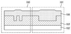
도 1a 내지 도 1d는 종래 기술에 따른 반도체 소자 형성 방법을 설명하기 위한 단면도이다.1A to 1D are cross-sectional views illustrating a method of forming a semiconductor device according to the prior art.
도 1a에서 나타낸 바와 같이, 셀(cell) 영역(100) 및 스크라이브 레인(Scribe lane) 영역(101)을 구비하는 반도체 기판(102) 상에 ILD(Inter-Layer Dielectric) 막(103)을 형성하고 ILD막(103) 상에 적어도 하나 이상의 트렌치(104)(105)를 형성하기 위하여 포토 레지스트 물질을 도포한 후 패터닝하여 포토 레지스트 패턴을 형성한다.As shown in FIG. 1A, an ILD (Inter-Layer Dielectric)
이 후, 포토 레지스트 패턴을 이용하는 식각 공정을 수행하여 셀 영역(100)의 트렌치(104)보다 폭이 넓은 트렌치(105)를 스크라이브 레인 영역(101)에 형성한 후 애싱 및 세정공정을 수행하여 포토 레지스트 패턴을 제거한다.Thereafter, an etching process using a photoresist pattern is performed to form
도 1b 및 도 1c에서 나타낸 바와 같이, 적어도 하나 이상의 트렌치(104)(105)를 포함하는 반도체 기판(102) 전면에 전기도금법(EP:eletro-plating)으로 구리막(106)을 증착하여 트렌치(104)(105)들을 충진하고 구리막(106)에 대하여 화학 기계적 연마(CMP:chemical mechanical polishing) 방법으로 평탄화를 수행하여 구리막 패턴(106a)을 형성한다.As shown in FIGS. 1B and 1C, a
도 1d에서 나타낸 바와 같이, 구리막 패턴(106a) 상에 다마신 공정(damascene) 방법으로 알루미늄 막(107)을 증착한다.As shown in FIG. 1D, the
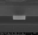
그러나, 도 2a 및 도2b에서 나타낸 바와 같이, 스크라이브 레인(Scribe lane) 영역(101)에 구리막 패턴(106a)과 알루미늄막(107) 간에 토폴로지(topology)가 없어, 도 3에서 나타낸 바와 같이 알루미늄막(107)에 의해 패터닝(patterning) 을 위해 포토 리소그라피(Photolithography) 공정을 위한 얼라인(align) 수행을 할 수 없는 문제점이 있다.However, as shown in FIG. 2A and FIG. 2B, there is no topology between the
본 발명은 상술한 바와 같은 종래 기술의 문제점을 해결하기 위하여 제안된 것으로, 얼라인(align) 및 오버레이 키(overlay key) 영역 형성 공정을 줄이는 반도체 소자 형성 방법을 제공하는 데 목적이 있다.SUMMARY OF THE INVENTION The present invention has been proposed to solve the problems of the prior art as described above, and an object thereof is to provide a method of forming a semiconductor device which reduces an alignment and overlay key area forming process.
전술한 목적을 달성하기 위한 본 발명의 특징은 반도체 기판 위에 ILD(Inter-Layer Dielectric)막을 형성하는 단계와, 상기 ILD막에 셀 영역의 제1 트렌치 또는 비아(via) 보다 폭이 넓은 제2 트렌치를 형성하는 단계와, 상기 제1 트렌치 또는 비아(via) 및 상기 제2 트렌치를 포함하는 반도체 기판에 제1 금속막을 증착하는 단계와, 상기 셀 영역의 제1 트렌치 또는 비아(via)에 상기 제1 금속막이 충진된 경우에 상기 제1 금속막 증착을 중단하는 단계와, 상기 제1 금속막에 대하여 평탄화를 수행하여 상기 제2 트렌치에 토폴로지(topology)를 갖는 제1 금속막 패턴을 형성하는 단계와, 상기 반도체 기판 전면에 제2 금속막을 증착하여 상기 토폴로지(topology)를 갖는 상기 제1 금속막 패턴에 의해 다수의 얼라인 및 오버레이 키 영역을 형성하는 단계를 포함하는 반도체 소자 형성 방법에 관한 것이다.A feature of the present invention for achieving the above object is the step of forming an inter-layer dielectric (ILD) film on a semiconductor substrate, the second trench wider than the first trench or via of the cell region in the ILD film Forming a first metal film on the semiconductor substrate including the first trench or via and the second trench, and forming the first trench or via in the cell region. 1, when the metal film is filled, stopping the deposition of the first metal film, and performing planarization on the first metal film to form a first metal film pattern having a topology in the second trench. And forming a plurality of alignment and overlay key regions by the first metal layer pattern having the topology by depositing a second metal layer on the entire surface of the semiconductor substrate. It is about a method.
본 발명에서 상기 셀 영역의 제1 트렌치는 0.1~0.5㎛의 폭으로 형성하고, 상기 제2 트렌치는 1~10㎛의 폭으로 형성하는 것을 특징으로 한다.In the present invention, the first trench of the cell region is formed in a width of 0.1 ~ 0.5㎛, the second trench is characterized in that it is formed in a width of 1 ~ 10㎛.
본 발명에서 상기 제1 금속막은 구리(Cu), 은(Ag) 및 알루미늄(Al) 중에서 적어도 하나로 형성하는 것을 특징으로 한다.In the present invention, the first metal layer is formed of at least one of copper (Cu), silver (Ag), and aluminum (Al).
본 발명에서 상기 제2 금속막은 알루미늄(Al)막으로 형성하는 것을 특징으로 한다.In the present invention, the second metal film is formed of an aluminum (Al) film.
이하에서 첨부된 도면을 참조하여 본 발명에 따른 반도체 소자 형성 방법에 대해서 상세히 설명한다.Hereinafter, a method of forming a semiconductor device according to the present invention will be described in detail with reference to the accompanying drawings.
도 4a 내지 도 4d는 본 발명에 따른 반도체 형성 방법을 설명하기 위한 단면도들이다.4A to 4D are cross-sectional views illustrating a method of forming a semiconductor in accordance with the present invention.
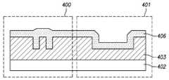
도 4a에서 나타낸 바와 같이, 셀(Cell) 영역(400) 또는 스크라이브 레인(Scribe lane) 영역(401)을 구비한 반도체 기판(402) 위에 ILD((Inter-Layer Dielectric) 막(403)을 형성하고 ILD 막(403) 위에 적어도 하나 이상의 트렌치를 형성하기 위하여 포토 레지스트 물질을 도포한 후 패터닝하여 포토 레지스트 패턴을 형성한다.As shown in FIG. 4A, an ILD (Inter-Layer Dielectric)
이 후, 포토 레지스트 패턴을 마스크로 이용하는 식각 공정을 수행하여 셀 영역(400)의 트렌치(404)보다 폭이 넓은 트렌치(405)를 스크라이브 레인 영역(401)에 형성한 후 애싱 및 세정공정을 수행하여 포토 레지스트 패턴을 제거한다.Subsequently, an etching process using the photoresist pattern as a mask is performed to form
여기서, 셀 영역(400)의 트렌치(404)는 예컨대, 0.1~0.5㎛의 폭으로 형성하고, 스크라이브 라인 영역(401)의 트렌치(405)는 예컨대, 1~10㎛의 폭으로 형성하는 것이 바람직하다.Here, the
도 4b 및 도 4c에서 나타낸 바와 같이, 셀 영역(400) 및 스크라이브 레인 영역(401)의 트렌치(404)(405)를 포함하는 반도체 기판(402) 전면에 전기 도금 법(EP:eletro-plating)으로 제1 금속막(406)을 증착하는 동안에 셀 영역(400)의 트렌치(404) 내에 제1 금속막(406)이 다 충진되는 경우에 제1 금속막(406) 증착을 중단한 후 제1 금속막(406)에 대하여 화학 기계적 연마(CMP:chemical mechanical polishing) 방법으로 평탄화를 수행하여 스크라이브 레인 영역(401)에 토폴로지(topology)를 갖는 제1 금속막 패턴(406a)을 형성한다.As shown in FIGS. 4B and 4C, electro-plating (EP) on the entire surface of the
여기서, 제1 금속막(406)은 구리(Cu), 은(Ag), 알루미늄(Al) 중에서 적어도 하나로 형성할 수 있다.The
이때, 스크라이브 라인 영역(401)의 트렌치(405)에는 셀 영역(400)의 트렌치(404) 보다 폭이 넓어 제1 금속막(406)을 다 충진되지 않는다.In this case, the
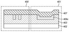
도 4d에서 나타낸 바와 같이, 트렌치(404)(405)를 구비하는 반도체 기판(402) 전면에 제2 금속막(407) 예컨대, 알루미늄(Al)막을 증착한다.As shown in FIG. 4D, a
여기서, 스크라이브 라인 영역(401)의 트렌치(405)에서 제2금속막(407)은 제1 금속막 패턴(406a)의 토폴로지(topology)에 의해 제2 금속막(407)에도 토폴로지(topology)가 형성되어 포토 리소그라피(Photolithography) 공정에서 오버레이(overlay) 또는 얼라인(align)을 수행할 수 있다.Here, in the
또한, 제1 금속막(405)과 제2 금속막 간에 토폴로지(topology)가 형성되어 얼라인 및 오버레이 키 영역 형성 공정을 줄일 수도 있다.In addition, a topology may be formed between the
즉, 도 5a에서 나타낸 바와 같이, 셀 영역의 트렌치 패턴에 제1금속막이 필(fill) 되어 있고, 도 5b에서 나타낸 바와 같이, 스크라이브 레인 영역의 트렌치에 제1 금속막과 제2 금속막 간에 토폴로지가 형성되는 것을 알 수 있으며 트렌치 공정에도 적용이 가능하다.That is, as shown in FIG. 5A, the first metal film is filled in the trench pattern of the cell region, and as shown in FIG. 5B, the topology between the first metal film and the second metal film is formed in the trench of the scribe lane region. It can be seen that is formed and can be applied to the trench process.
또한, 도 6a에서 나타낸 바와 같이, 셀 영역의 비아 패턴에 제1금속막이 필(fill) 되어 있고, 도 6b에서 나타낸 바와 같이, 스크라이브 레인 영역의 트렌치에 제1 금속막과 제2 금속막 간에 토폴로지가 형성되는 것을 알 수 있으며 비아 공정에도 적용이 가능하다.In addition, as shown in FIG. 6A, the first metal film is filled in the via pattern of the cell region, and as shown in FIG. 6B, a topology between the first metal film and the second metal film is formed in the trench of the scribe lane region. It can be seen that is formed and can be applied to the via process.
따라서, 도 7a 내지 도 7b에서 나타낸 바와 같이, 스크라이브 레인 영역의 제1 금속막과 제2 금속막 간에 토폴로지가 형성되어 이전 층의 얼라인 키, 이전 층의 오버 레이 키 및 현재 층의 오버 레이 키를 확인할 수 있다.Thus, as shown in Figs. 7A to 7B, a topology is formed between the first metal film and the second metal film in the scribe lane region so that the alignment key of the previous layer, the overlay key of the previous layer, and the overlay key of the current layer are shown. You can check.
이상과 같이 본 발명은 비록 한정된 실시 예와 도면에 의해 설명되었으나, 본 발명은 상기의 실시 예에 한정되는 것이 아니며, 본 발명이 속하는 분야에서 통상의 지식을 가진 자라면, 이러한 기재로부터 다양한 수정 및 변형이 가능하다.As described above, although the present invention has been described with reference to the limited embodiments and the drawings, the present invention is not limited to the above embodiments, and those skilled in the art to which the present invention pertains can make various modifications and Modifications are possible.
그러므로, 본 발명의 범위는 설명된 실시 예에 국한되어 정해져서는 아니되며, 후술하는 특허청구범위뿐만 아니라 이 특허 청구범위와 균등한 것들에 의해 정해져야 한다.Therefore, the scope of the present invention should not be limited to the described embodiments, but should be determined not only by the claims below but also by the equivalents of the claims.
이상에서 설명한 바와 같이, 본 발명에 따른 반도체 소자 형성 방법에 따라 제1 금속막과 제2 금속막 간에 토폴로지(topology)를 형성함으로써, 패터닝(patterning)을 위해 포토 리소그라피(Photolithography) 위한 얼라인(align)을 수행할 수 있는 효과가 있다.As described above, by forming a topology between the first metal film and the second metal film according to the method of forming a semiconductor device according to the present invention, alignment for photolithography for patterning is performed. ) Is effective.
또한, 본 발명은 스크라이브 레인(Scribe lane) 영역의 얼라인 및 오버레이 키 영역 형성 공정을 줄일 수 있는 효과가 있다.In addition, the present invention has the effect of reducing the alignment and overlay key region forming process of the scribe lane area.
Claims (4)
Translated fromKoreanPriority Applications (2)
| Application Number | Priority Date | Filing Date | Title |
|---|---|---|---|
| KR1020060137334AKR100831267B1 (en) | 2006-12-29 | 2006-12-29 | Semiconductor device formation method |
| US11/944,231US20080160714A1 (en) | 2006-12-29 | 2007-11-21 | Method of forming semiconductor device |
Applications Claiming Priority (1)
| Application Number | Priority Date | Filing Date | Title |
|---|---|---|---|
| KR1020060137334AKR100831267B1 (en) | 2006-12-29 | 2006-12-29 | Semiconductor device formation method |
Publications (1)
| Publication Number | Publication Date |
|---|---|
| KR100831267B1true KR100831267B1 (en) | 2008-05-22 |
Family
ID=39584586
Family Applications (1)
| Application Number | Title | Priority Date | Filing Date |
|---|---|---|---|
| KR1020060137334AExpired - Fee RelatedKR100831267B1 (en) | 2006-12-29 | 2006-12-29 | Semiconductor device formation method |
Country Status (2)
| Country | Link |
|---|---|
| US (1) | US20080160714A1 (en) |
| KR (1) | KR100831267B1 (en) |
Cited By (1)
| Publication number | Priority date | Publication date | Assignee | Title |
|---|---|---|---|---|
| US9911802B2 (en) | 2015-03-27 | 2018-03-06 | Samsung Display Co., Ltd. | Display device and method for manufacturing the same |
Families Citing this family (2)
| Publication number | Priority date | Publication date | Assignee | Title |
|---|---|---|---|---|
| JP5432481B2 (en)* | 2008-07-07 | 2014-03-05 | ルネサスエレクトロニクス株式会社 | Semiconductor device manufacturing method and semiconductor device |
| KR101233947B1 (en)* | 2011-11-28 | 2013-02-15 | 주식회사 동부하이텍 | Semiconductor device and method of fabricatig the same |
Citations (2)
| Publication number | Priority date | Publication date | Assignee | Title |
|---|---|---|---|---|
| KR20020010791A (en)* | 2000-07-31 | 2002-02-06 | 박종섭 | Manufacturing method for semiconductor device |
| KR20060025073A (en)* | 2004-09-15 | 2006-03-20 | 주식회사 하이닉스반도체 | Method of forming a semiconductor device |
Family Cites Families (1)
| Publication number | Priority date | Publication date | Assignee | Title |
|---|---|---|---|---|
| JP3609761B2 (en)* | 2001-07-19 | 2005-01-12 | 三洋電機株式会社 | Manufacturing method of semiconductor device |
- 2006
- 2006-12-29KRKR1020060137334Apatent/KR100831267B1/ennot_activeExpired - Fee Related
- 2007
- 2007-11-21USUS11/944,231patent/US20080160714A1/ennot_activeAbandoned
Patent Citations (2)
| Publication number | Priority date | Publication date | Assignee | Title |
|---|---|---|---|---|
| KR20020010791A (en)* | 2000-07-31 | 2002-02-06 | 박종섭 | Manufacturing method for semiconductor device |
| KR20060025073A (en)* | 2004-09-15 | 2006-03-20 | 주식회사 하이닉스반도체 | Method of forming a semiconductor device |
Cited By (1)
| Publication number | Priority date | Publication date | Assignee | Title |
|---|---|---|---|---|
| US9911802B2 (en) | 2015-03-27 | 2018-03-06 | Samsung Display Co., Ltd. | Display device and method for manufacturing the same |
Also Published As
| Publication number | Publication date |
|---|---|
| US20080160714A1 (en) | 2008-07-03 |
Similar Documents
| Publication | Publication Date | Title |
|---|---|---|
| US9543193B2 (en) | Non-hierarchical metal layers for integrated circuits | |
| US7977237B2 (en) | Fabricating vias of different size of a semiconductor device by splitting the via patterning process | |
| KR100901054B1 (en) | Semiconductor device and manufacturing method of semiconductor device | |
| KR100831267B1 (en) | Semiconductor device formation method | |
| KR100525014B1 (en) | Method for applying adjusting marks on a semiconductor disk | |
| US20080122116A1 (en) | Method of forming metal layer wiring structure on backside of wafer, metal layer wiring structure formed using the method, method of stacking chip package, and chip package stack structure formed using the method | |
| US7575980B2 (en) | Semiconductor device and method for manufacturing the same | |
| KR100849358B1 (en) | Method for Menufaturing Align Key of Semiconductor Divice | |
| JP3408746B2 (en) | Method for manufacturing semiconductor device | |
| KR100800786B1 (en) | Overlay Marks for Forming Multi-layered Metal Wiring in Semiconductor Devices | |
| US20070069387A1 (en) | Semiconductor device and method of forming the same | |
| KR100995142B1 (en) | Contact hole formation method of semiconductor device | |
| JPH1174174A (en) | Method for manufacturing semiconductor device | |
| KR100879885B1 (en) | Manufacturing Method of Semiconductor Device | |
| KR20080070215A (en) | Alignment Marks and Methods for Making the Same | |
| US6383930B1 (en) | Method to eliminate copper CMP residue of an alignment mark for damascene processes | |
| KR100349696B1 (en) | Method of forming damascene structure for metal interconnection of semiconductor device using chemical swelling process | |
| KR100887019B1 (en) | Mask with multiple overlay marks | |
| KR100248809B1 (en) | Method of manufacturing semiconductor device | |
| US20080023736A1 (en) | Semiconductor Device and Method for Manufacturing the Same | |
| KR100702801B1 (en) | Metal wiring formation method using dual damascene process | |
| CN118173502A (en) | Method for improving metal layer alignment precision and semiconductor structure | |
| KR101882851B1 (en) | Method for fabricating semiconductor device | |
| US20080272459A1 (en) | Semiconductor Device and Manufacturing Method of Semiconductor Device | |
| KR19990006078A (en) | Method of forming overlay measurement mark of semiconductor device |
Legal Events
| Date | Code | Title | Description |
|---|---|---|---|
| A201 | Request for examination | ||
| PA0109 | Patent application | St.27 status event code:A-0-1-A10-A12-nap-PA0109 | |
| PA0201 | Request for examination | St.27 status event code:A-1-2-D10-D11-exm-PA0201 | |
| R17-X000 | Change to representative recorded | St.27 status event code:A-3-3-R10-R17-oth-X000 | |
| E902 | Notification of reason for refusal | ||
| PE0902 | Notice of grounds for rejection | St.27 status event code:A-1-2-D10-D21-exm-PE0902 | |
| P11-X000 | Amendment of application requested | St.27 status event code:A-2-2-P10-P11-nap-X000 | |
| P13-X000 | Application amended | St.27 status event code:A-2-2-P10-P13-nap-X000 | |
| E701 | Decision to grant or registration of patent right | ||
| PE0701 | Decision of registration | St.27 status event code:A-1-2-D10-D22-exm-PE0701 | |
| GRNT | Written decision to grant | ||
| PR0701 | Registration of establishment | St.27 status event code:A-2-4-F10-F11-exm-PR0701 | |
| PR1002 | Payment of registration fee | St.27 status event code:A-2-2-U10-U11-oth-PR1002 Fee payment year number:1 | |
| PG1601 | Publication of registration | St.27 status event code:A-4-4-Q10-Q13-nap-PG1601 | |
| PR1001 | Payment of annual fee | St.27 status event code:A-4-4-U10-U11-oth-PR1001 Fee payment year number:4 | |
| FPAY | Annual fee payment | Payment date:20120417 Year of fee payment:5 | |
| PR1001 | Payment of annual fee | St.27 status event code:A-4-4-U10-U11-oth-PR1001 Fee payment year number:5 | |
| LAPS | Lapse due to unpaid annual fee | ||
| PC1903 | Unpaid annual fee | St.27 status event code:A-4-4-U10-U13-oth-PC1903 Not in force date:20130516 Payment event data comment text:Termination Category : DEFAULT_OF_REGISTRATION_FEE | |
| PC1903 | Unpaid annual fee | St.27 status event code:N-4-6-H10-H13-oth-PC1903 Ip right cessation event data comment text:Termination Category : DEFAULT_OF_REGISTRATION_FEE Not in force date:20130516 |