KR100830128B1 - Laser system and method for processing memory links with bursts of laser pulses with very short pulse widths - Google Patents
Laser system and method for processing memory links with bursts of laser pulses with very short pulse widthsDownload PDFInfo
- Publication number
- KR100830128B1 KR100830128B1KR1020027008432AKR20027008432AKR100830128B1KR 100830128 B1KR100830128 B1KR 100830128B1KR 1020027008432 AKR1020027008432 AKR 1020027008432AKR 20027008432 AKR20027008432 AKR 20027008432AKR 100830128 B1KR100830128 B1KR 100830128B1
- Authority
- KR
- South Korea
- Prior art keywords
- laser
- link
- laser output
- output pulses
- abandoned
- Prior art date
- Legal status (The legal status is an assumption and is not a legal conclusion. Google has not performed a legal analysis and makes no representation as to the accuracy of the status listed.)
- Expired - Fee Related
Links
Images


Classifications
- H—ELECTRICITY
- H01—ELECTRIC ELEMENTS
- H01S—DEVICES USING THE PROCESS OF LIGHT AMPLIFICATION BY STIMULATED EMISSION OF RADIATION [LASER] TO AMPLIFY OR GENERATE LIGHT; DEVICES USING STIMULATED EMISSION OF ELECTROMAGNETIC RADIATION IN WAVE RANGES OTHER THAN OPTICAL
- H01S5/00—Semiconductor lasers
- H01S5/06—Arrangements for controlling the laser output parameters, e.g. by operating on the active medium
- H—ELECTRICITY
- H01—ELECTRIC ELEMENTS
- H01L—SEMICONDUCTOR DEVICES NOT COVERED BY CLASS H10
- H01L23/00—Details of semiconductor or other solid state devices
- H01L23/52—Arrangements for conducting electric current within the device in operation from one component to another, i.e. interconnections, e.g. wires, lead frames
- H01L23/522—Arrangements for conducting electric current within the device in operation from one component to another, i.e. interconnections, e.g. wires, lead frames including external interconnections consisting of a multilayer structure of conductive and insulating layers inseparably formed on the semiconductor body
- H01L23/525—Arrangements for conducting electric current within the device in operation from one component to another, i.e. interconnections, e.g. wires, lead frames including external interconnections consisting of a multilayer structure of conductive and insulating layers inseparably formed on the semiconductor body with adaptable interconnections
- H01L23/5256—Arrangements for conducting electric current within the device in operation from one component to another, i.e. interconnections, e.g. wires, lead frames including external interconnections consisting of a multilayer structure of conductive and insulating layers inseparably formed on the semiconductor body with adaptable interconnections comprising fuses, i.e. connections having their state changed from conductive to non-conductive
- H01L23/5258—Arrangements for conducting electric current within the device in operation from one component to another, i.e. interconnections, e.g. wires, lead frames including external interconnections consisting of a multilayer structure of conductive and insulating layers inseparably formed on the semiconductor body with adaptable interconnections comprising fuses, i.e. connections having their state changed from conductive to non-conductive the change of state resulting from the use of an external beam, e.g. laser beam or ion beam
- B—PERFORMING OPERATIONS; TRANSPORTING
- B23—MACHINE TOOLS; METAL-WORKING NOT OTHERWISE PROVIDED FOR
- B23K—SOLDERING OR UNSOLDERING; WELDING; CLADDING OR PLATING BY SOLDERING OR WELDING; CUTTING BY APPLYING HEAT LOCALLY, e.g. FLAME CUTTING; WORKING BY LASER BEAM
- B23K26/00—Working by laser beam, e.g. welding, cutting or boring
- B23K26/02—Positioning or observing the workpiece, e.g. with respect to the point of impact; Aligning, aiming or focusing the laser beam
- B23K26/04—Automatically aligning, aiming or focusing the laser beam, e.g. using the back-scattered light
- B—PERFORMING OPERATIONS; TRANSPORTING
- B23—MACHINE TOOLS; METAL-WORKING NOT OTHERWISE PROVIDED FOR
- B23K—SOLDERING OR UNSOLDERING; WELDING; CLADDING OR PLATING BY SOLDERING OR WELDING; CUTTING BY APPLYING HEAT LOCALLY, e.g. FLAME CUTTING; WORKING BY LASER BEAM
- B23K26/00—Working by laser beam, e.g. welding, cutting or boring
- B23K26/02—Positioning or observing the workpiece, e.g. with respect to the point of impact; Aligning, aiming or focusing the laser beam
- B23K26/06—Shaping the laser beam, e.g. by masks or multi-focusing
- B23K26/062—Shaping the laser beam, e.g. by masks or multi-focusing by direct control of the laser beam
- B23K26/0622—Shaping the laser beam, e.g. by masks or multi-focusing by direct control of the laser beam by shaping pulses
- B23K26/0624—Shaping the laser beam, e.g. by masks or multi-focusing by direct control of the laser beam by shaping pulses using ultrashort pulses, i.e. pulses of 1ns or less
- G—PHYSICS
- G03—PHOTOGRAPHY; CINEMATOGRAPHY; ANALOGOUS TECHNIQUES USING WAVES OTHER THAN OPTICAL WAVES; ELECTROGRAPHY; HOLOGRAPHY
- G03F—PHOTOMECHANICAL PRODUCTION OF TEXTURED OR PATTERNED SURFACES, e.g. FOR PRINTING, FOR PROCESSING OF SEMICONDUCTOR DEVICES; MATERIALS THEREFOR; ORIGINALS THEREFOR; APPARATUS SPECIALLY ADAPTED THEREFOR
- G03F7/00—Photomechanical, e.g. photolithographic, production of textured or patterned surfaces, e.g. printing surfaces; Materials therefor, e.g. comprising photoresists; Apparatus specially adapted therefor
- G03F7/70—Microphotolithographic exposure; Apparatus therefor
- G03F7/70008—Production of exposure light, i.e. light sources
- G03F7/70041—Production of exposure light, i.e. light sources by pulsed sources, e.g. multiplexing, pulse duration, interval control or intensity control
- G—PHYSICS
- G03—PHOTOGRAPHY; CINEMATOGRAPHY; ANALOGOUS TECHNIQUES USING WAVES OTHER THAN OPTICAL WAVES; ELECTROGRAPHY; HOLOGRAPHY
- G03F—PHOTOMECHANICAL PRODUCTION OF TEXTURED OR PATTERNED SURFACES, e.g. FOR PRINTING, FOR PROCESSING OF SEMICONDUCTOR DEVICES; MATERIALS THEREFOR; ORIGINALS THEREFOR; APPARATUS SPECIALLY ADAPTED THEREFOR
- G03F7/00—Photomechanical, e.g. photolithographic, production of textured or patterned surfaces, e.g. printing surfaces; Materials therefor, e.g. comprising photoresists; Apparatus specially adapted therefor
- G03F7/70—Microphotolithographic exposure; Apparatus therefor
- G03F7/70691—Handling of masks or workpieces
- G03F7/70716—Stages
- G03F7/70725—Stages control
- H—ELECTRICITY
- H01—ELECTRIC ELEMENTS
- H01L—SEMICONDUCTOR DEVICES NOT COVERED BY CLASS H10
- H01L21/00—Processes or apparatus adapted for the manufacture or treatment of semiconductor or solid state devices or of parts thereof
- H01L21/70—Manufacture or treatment of devices consisting of a plurality of solid state components formed in or on a common substrate or of parts thereof; Manufacture of integrated circuit devices or of parts thereof
- H01L21/71—Manufacture of specific parts of devices defined in group H01L21/70
- H01L21/768—Applying interconnections to be used for carrying current between separate components within a device comprising conductors and dielectrics
- H01L21/76838—Applying interconnections to be used for carrying current between separate components within a device comprising conductors and dielectrics characterised by the formation and the after-treatment of the conductors
- H01L21/76886—Modifying permanently or temporarily the pattern or the conductivity of conductive members, e.g. formation of alloys, reduction of contact resistances
- H01L21/76892—Modifying permanently or temporarily the pattern or the conductivity of conductive members, e.g. formation of alloys, reduction of contact resistances modifying the pattern
- H01L21/76894—Modifying permanently or temporarily the pattern or the conductivity of conductive members, e.g. formation of alloys, reduction of contact resistances modifying the pattern using a laser, e.g. laser cutting, laser direct writing, laser repair
- H—ELECTRICITY
- H01—ELECTRIC ELEMENTS
- H01L—SEMICONDUCTOR DEVICES NOT COVERED BY CLASS H10
- H01L2924/00—Indexing scheme for arrangements or methods for connecting or disconnecting semiconductor or solid-state bodies as covered by H01L24/00
- H01L2924/0001—Technical content checked by a classifier
- H01L2924/0002—Not covered by any one of groups H01L24/00, H01L24/00 and H01L2224/00
Landscapes
- Physics & Mathematics (AREA)
- Optics & Photonics (AREA)
- Engineering & Computer Science (AREA)
- General Physics & Mathematics (AREA)
- Plasma & Fusion (AREA)
- Mechanical Engineering (AREA)
- Condensed Matter Physics & Semiconductors (AREA)
- Microelectronics & Electronic Packaging (AREA)
- Computer Hardware Design (AREA)
- Power Engineering (AREA)
- Manufacturing & Machinery (AREA)
- Electromagnetism (AREA)
- Lasers (AREA)
- Laser Beam Processing (AREA)
- Design And Manufacture Of Integrated Circuits (AREA)
- Semiconductor Memories (AREA)
- Manufacturing Of Printed Wiring (AREA)
Abstract
Translated fromKoreanDescription
Translated fromKorean본 발명은 메모리 또는 다른 IC 링크의 레이저 처리에 관한 것으로, 특히, IC 링크를 절단하기 위해서 초단 펄스 폭을 가진 레이저 펄스의 버스트를 사용하는 레이저 시스템 및 방법에 관한 것이다.TECHNICAL FIELD The present invention relates to laser processing of memory or other IC links, and more particularly, to laser systems and methods that use bursts of laser pulses with ultra short pulse widths to cut IC links.
IC 디바이스 제작 공정에서의 수율(yield)은 종종 하부표면 층이나 패턴의 정렬 변동 또는 미립자 오염물질로 인해 발생하는 결함의 영향을 받는다. 도 1, 2a 및 2b는 메모리 셀(20)의 예비 행(16) 및 열(18)과 같은 중복 회로 소자(14)의 다중 반복을 포함하도록 일반적으로 행 또는 열로 제작되는 IC 디바이스나 워크피스(12)의 반복 전자 회로(10)를 도시하고 있다. 도 1, 2a 및 2b를 참조하면, 회로(10)는 또한 예컨대 결함이 있는 메모리 셀(20)을 연결해제시키기 위해서 제거될 수 있는 전기적인 접촉부(24) 사이에 특별한 레이저 절단가능 회로 링크(22)를 포함하고 DRAM, SRAM, 또는 삽입된 메모리와 같은 메모리 디바이스에서 교체 중복 셀(26)을 교체하도록 설계된다. 유사한 기술이 논리곱, 게이트 어레이, 또는 ASICs를 프로그램하기 위해 링크를 절단하는데 또한 사용된다.Yields in IC device fabrication processes are often affected by defects caused by misalignment of the subsurface layer or pattern or particulate contaminants. 1, 2A and 2B illustrate IC devices or workpieces typically fabricated in rows or columns to include multiple iterations of
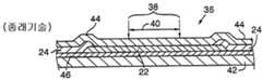
링크(22)는, 링크 구조(36)와 같이, 대략 0.5 내지 2 미크론(㎛)의 두께를 갖고, 대략 0.8 내지 2.5 ㎛의 종래 링크 폭(28), 링크 길이(30) 및 인접한 회로 구조나 소자(34)로부터 대략 2 내지 8 ㎛의 소자간 이격거리(중심간 떨어진 간격)(32)를 갖도록 설계된다. 비록 가장 일반적으로 사용되는 링크 물질은 폴리실리콘 및 그와 유사한 혼합물이지만, 메모리 제작자들은 더욱 최근에는, 알루미늄, 구리, 금 니켈, 티타늄, 텅스텐, 백금뿐만 아니라 다른 금속들, 금속 합금, 티타늄이나 탄탈 질화물과 같은 금속 질화물, 텅스텐 실리사이드와 같은 금속 실리사이드, 또는 다른 금속-유사 물질을 포함할 수 있지만 그러한 물질들로 제한되지는 않는 다양한 종류의 더욱 전도적인 금속 링크 물질을 채택하고 있다.The
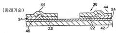
회로(10), 회로 소자(14), 또는 셀(20)은 결함 여부에 대해서 테스트되고, 그것들의 위치는 데이터베이스나 프로그램에 매핑될 수 있다. 전통적인 1.047 ㎛ 또는 1.064 ㎛의 적외선(IR) 레이저 파장이 회로 링크(22)를 폭발적으로 제거하기 위해서 20년 이상 사용되어 오고 있다. 종래의 메모리 링크 처리 시스템은 대략 4 내지 20 ㎱의 펄스 폭을 갖는 레이저 출력의 단일 펄스를 각각의 링크(22)에 집속시킨다. 도 2a 및 2b는, 실리콘 기판(42) 위에 위치하면서 위에 있는 보호막 층(44)(도 2a에는 도시되어 있지만 도 2b에는 도시되어 있지 않음)(전형적으로 2000 내지 10,000 Å의 두께를 가짐)을 포함하는 보호막 층 스택의 소자 층과 아래에 있는 보호막 층(46) 사이에 위치하는 폴리실리콘 또는 금속 링크(22)로 구성된 링크 구조(36)에 충돌하는 스폿 크기 직경(40)의 레이저 스폿(38)을 도시하고 있다. 실리콘 기판(42)은 IR 방사의 비교적 작은 비례적인 양을 흡수하고, 이산화 규 소나 질화 규소와 같은 종래의 보호막 층(44 및 46)은 IR 방사에 대해서 비교적 투명하다. 도 2c는 링크(22)가 종래의 레이저 펄스에 의해서 제거된 이후에 도 2b의 링크 구조에 대한 단편적인 단면도이다.
금속 또는 비금속 링크(22)를 처리하기에 충분한 에너지를 유지하면서 기판(42)에 손상을 주는 것을 회피하기 위해서, 선(Sun) 등에 의한 미국 특허 제 5,265,114호 및 제 5,473,624호에서는 실리콘 웨이퍼 상의 메모리 링크(22)를 처리하기 위해 1.3 ㎛와 같은 더 긴 레이저 파장에서 단일의 9 내지 25 ㎱ 펄스를 사용하는 것을 제안하였다. 1.3 ㎛ 레이저 파장에서, 링크 물질과 실리콘 기판(42) 사이의 흡수 대비(absorption contrast)는 전통적인 1 ㎛ 레이저 파장에서의 흡수 대비 보다 훨씬 더 크다. 이러한 기술에 의해서 제공되는 훨씬 더 넓은 레이저 처리 윈도우 및 더 나은 처리 품질은 대략 3년 동안에 산업계에서 큰 성과를 이루면서 사용되어 왔다.In order to avoid damaging the
그러나, 1.0 ㎛ 및 1.3 ㎛ 레이저 파장은 단점을 가지고 있다. 매우 전기 전도적인 금속 링크(22)로의 그러한 IR 레이저 빔의 연결 효율은 비교적 나쁘고, 링크 절단을 위한 IR 레이저 빔의 실제로 획득가능한 스폿 크기(38)는 비교적 크며, 링크 폭(28), 접촉부(24) 사이의 링크 길이(30), 및 링크 이격거리(32)의 임계치수를 제한한다. 이러한 종래의 레이저 링크 처리는 링크(22)를 가열, 용해, 및 증착(evaporate)시키는 것과, 위에 있는 보호막 층(44)을 폭발적으로 오픈시키기 위해서 기계적인 응력 증강을 생성하는 것에 의지한다. 그러한 종래의 링크 처리용 레이저 펄스는 절단된 링크를 포함하는 디바이스의 품질을 저하시키는 큰 열영향 구역(HAZ : Heat Affected Zone)을 생성한다.However, 1.0 μm and 1.3 μm laser wavelengths have disadvantages. The efficiency of coupling such an IR laser beam to a highly electrically
열-응력 폭발 작용은 또한 링크(22)의 폭에 다소 의지한다. 링크 폭이 대략 1 ㎛ 보다 더 좁아졌을 때, 보호막 층(44)의 폭발 패턴은 불규칙적으로 되고, 용인가능하지 않은 회로 밀도를 제한하는 일관성 없는 링크 처리 품질을 초래한다. 따라서, 열-응력 작용은 링크(22)의 임계치수를 제한하고 더 큰 회로 밀도를 저지한다.The thermal stress explosion action also depends somewhat on the width of the
선(Sun) 등의 미국 특허 제 6,057,180호 및 스웬손(Swenson) 등의 미국 특허 제 6,025,256호에서는 더욱 최근에 다른 물질 제거 메커니즘에 의해서 위에 있는 보호막을 "오픈"시키고 더 작은 빔 스폿 크기의 이점을 갖는 링크를 절단하거나 노출시키기 위해서 자외선(UV) 레이저 출력을 사용하는 방법이 설명되어 있다. 그러나, 그러한 UV 레이저 펄스에 의한 링크 자체의 절개는 보호막 물질이 UV 흡수되는 것을 필요로 하고, 또한 "열" 처리이다.In US Pat. No. 6,057,180 to Sun et al. And US Pat. No. 6,025,256 to Swenson et al. More recently, other material removal mechanisms have “opened” the overcoat and benefit from smaller beam spot sizes. A method of using an ultraviolet (UV) laser power to cut or expose a link having is described. However, the incision of the link itself by such a UV laser pulse requires the protective film material to be UV absorbed and is also a "heat" treatment.
무로우(Mourou) 등의 미국 특허 제 5,656,186호에서는 높은 반복 속도의 초고속 레이저 펄스에 의한 레이저 유도 브레이크다운 및 제거(ablation)의 일반적인 방법을 개시하고 있다.U.S. Patent No. 5,656,186 to Mourou et al. Discloses a general method of laser induced breakdown and ablation by high repetition rate ultrafast laser pulses.
미요우치(Miyauchi) 등의 미국 특허 제 5,208,437호에서는 링크를 처리하기 위해서 나노세컨드 이하의 펄스 폭(subnanosecond pulse width)을 갖는 단일 펄스를 사용하는 방법을 개시하고 있다.U.S. Patent No. 5,208,437 to Miyauchi et al. Discloses a method of using a single pulse having a subnanosecond pulse width of less than nanoseconds to process a link.
리저(Rieger) 등의 미국 특허 제 5,742,634호에서는 다이오드 펌핑을 통해 일시에 Q-스위칭되고 모드-동기되는(simultaneously Q-switched and mode-locked) 네오디뮴(Nd) 레이저 디바이스를 개시하고 있다. 상기 레이저는 100 ㎱의 지속기간의 엔벌로프 하에서 60 내지 300 ㎰의 지속기간을 각각 갖는 일련의 펄스를 방출한다. 60 내지 300 ㎰의 지속기간을 갖는 펄스는 물질 처리의 "열" 메커니즘을 나타낸다.U.S. Patent No. 5,742,634 to Riger et al. Discloses a Q-switched and mode-locked neodymium (Nd) laser device that is instantaneously via diode pumping. The laser emits a series of pulses each having a duration of 60 to 300 Hz under an envelope of duration of 100 Hz. Pulses with a duration of 60 to 300 Hz represent a "heat" mechanism of material processing.
본 발명의 목적은 IC 링크의 레이저 처리 품질을 향상시키기 위한 방법이나 장치를 제공하는데 있다.It is an object of the present invention to provide a method or apparatus for improving the laser processing quality of an IC link.
본 발명의 또 다른 목적은 위에 있는 보호막 층 및 링크 물질과의 비-열적인 상호작용을 갖는 초단 레이저 펄스의 버스트로 링크를 처리하는데 있다.Yet another object of the present invention is to treat a link with a burst of ultrashort laser pulses having non-thermal interaction with the overlying protective layer and link material.
본 발명의 다른 목적은 진행 중에 링크를 처리하기 위해서 초단 레이저 펄스의 버스트를 사용하는데 있다.Another object of the present invention is to use a burst of ultrashort laser pulses to process the link in progress.
본 발명은 종래 링크 처리 시스템의 단일 다중-나노세컨드 레이저 펄스를 사용하는 대신에 IC 링크를 절단하기 위해서 초단 레이저 펄스의 버스트를 사용한다. 버스트의 지속기간은 바람직하게는 10 내지 500 ㎱의 범위에 있고, 버스트 내의 각 레이저 펄스의 펄스 폭은 일반적으로 25 ㎰ 보다 더 짧은데, 바람직하게는 10 ㎰ 보다 더 짧거나 그와 동일하고, 가장 바람직하게는 대략 10 ㎰ 내지 100 fs(femtoseconds)이다. 버스트 내의 각 레이저 펄스는 극히 짧기 때문에, 타겟 물질(보호막 층 및 금속 링크)과의 상호작용은 열적이지 않다. 각각의 레이저 펄스는, 링크가 절단될 때까지, 레이저 에너지, 레이저 파장 및 물질의 타입에 따라 물질의 대략 100 내지 2,000Å의 얇은 하부층을 절단한다. 버스트 내의 초단 레이저 펄스의 수는, 마지막 펄스가 밑에 있는 보호막 층과 기판이 손상되지 않도록 하면서 링크의 하단을 깨끗이 제거하도록 제어된다. 버스트의 전체 지속기간은 10 ㎱ 내지 500 ㎱의 범위에 있기 때문에, 버스트는 종래의 링크-절단용 레이저 위치지정 시스템에 의해서 단일 "펄스"인 것으로 간주된다. 따라서, 레이저 시스템은 여전히 진행 중에 링크를 처리할 수 있다. 즉 위치지정 시스템은 레이저 시스템이 각각의 링크에 레이저 펄스의 버스트를 발사할 때 이동하는 것을 멈출 필요가 없다.The present invention uses a burst of ultrashort laser pulses to cut the IC link instead of using a single multi-nanosecond laser pulse of a conventional link processing system. The duration of the burst is preferably in the range of 10 to 500 ms, and the pulse width of each laser pulse in the burst is generally shorter than 25 ms, preferably shorter or equal to 10 ms and most preferred. Preferably from about 10 μs to 100 fs (femtoseconds). Since each laser pulse in the burst is extremely short, the interaction with the target material (protective layer and metal link) is not thermal. Each laser pulse cuts a thin lower layer of approximately 100 to 2,000 microns of material, depending on the laser energy, laser wavelength, and type of material, until the link is cut. The number of ultrashort laser pulses in the burst is controlled to clean the bottom of the link without damaging the protective layer and substrate underneath the last pulse. Since the total duration of the burst is in the range of 10 Hz to 500 Hz, the burst is considered to be a single "pulse" by conventional link-cutting laser positioning systems. Thus, the laser system can still process the link in progress. That is, the positioning system does not need to stop moving when the laser system fires a burst of laser pulses on each link.
초단 펄스 레이저 처리의 "비-열적"이고 수월하게-제어가능한 특성 외에도, 가장 일반적인 초단-펄스 레이저 소스는 대략 800 ㎚의 파장에서 방출하고, 작은 크기의 레이저 스폿의 전달을 용이하게 한다. 바람직하게는, 다이오드-펌핑된, 즉 다이오드-펌핑된 고체-상태의 지속파(CW : Continuous Wave) 녹색 펌핑되고(green pumped) 모드-동기된 고체-상태 레이저가 종래의 파장이나 그것들의 고조파에서 초단 펄스를 생성하기 위해 사용된다.In addition to the "non-thermal" and easily-controllable nature of ultrashort pulsed laser processing, the most common ultrashort pulse sources emit at wavelengths of approximately 800 nm and facilitate the delivery of small size laser spots. Preferably, diode-pumped, ie diode-pumped, solid-state continuous wave (CW) green pumped and mode-synchronized solid-state lasers are used at conventional wavelengths or at their harmonics. Used to generate ultrashort pulses.
본 발명의 추가적인 목적 및 장점은 첨부 도면과 관련하여 시작될 본 발명의 바람직한 실시예에 대한 다음의 상세한 설명으로부터 자명해질 것이다.Further objects and advantages of the present invention will become apparent from the following detailed description of the preferred embodiments of the invention which will be taken in conjunction with the accompanying drawings.
도 1은 총체적인 회로 셀의 중복 배열 및 예비 행에서의 프로그램가능한 링크를 나타내는 DRAM의 부분에 대한 개략도.1 is a schematic diagram of a portion of a DRAM showing a redundant arrangement of overall circuit cells and programmable links in a spare row;
도 2a는 종래의 펄스 파라미터에 의해서 특징되는 레이저 펄스를 수신하는 종래의 대형 반도체 링크 구조에 대한 단편적인 단면도.2A is a fragmentary cross-sectional view of a conventional large semiconductor link structure that receives a laser pulse characterized by conventional pulse parameters.
도 2b는 인접한 회로 구조와 함께, 도 2a의 레이저 펄스 및 링크 구조에 대한 단편적인 평면도.FIG. 2B is a fragmentary plan view of the laser pulse and link structure of FIG. 2A, with adjacent circuit structures. FIG.
도 2c는 링크가 종래의 레이저 펄스에 의해서 제거된 이후의 도 2b의 링크 구조에 대한 단편적인 단면도.FIG. 2C is a fragmentary cross sectional view of the link structure of FIG. 2B after the link has been removed by a conventional laser pulse. FIG.
도 3은 본 발명에 따라 링크를 절단하기 위해서 사용되는 초단 레이저 펄스의 예시적인 버스트에 대한 전력 대 시간 그래프.3 is a power versus time graph for an exemplary burst of ultrashort laser pulses used to cut a link in accordance with the present invention.
도 4는 본 발명에 따라 링크를 절단하기 위해서 사용되는 초단 레이저 펄스의 대안적인 예시적 버스트의 전력 대 시간 그래프.4 is a power versus time graph of an alternative exemplary burst of ultrashort laser pulses used to cut a link in accordance with the present invention.
도 5는 본 발명에 따라 링크를 절단하기 위해서 사용되는 초단 레이저 펄스의 다른 대안적인 예시적 버스트의 전력 대 시간 그래프.5 is a power versus time graph of another alternative exemplary burst of ultrashort laser pulses used to cut a link in accordance with the present invention.
도 6은 본 발명의 방법을 실행하기 위해 레이저 처리 제어 시스템과 협력하는 워크피스 위치지정기를 포함하는 바람직한 UV 레이저 시스템의 일실시예를 부분적으로 나타내는 개략적인 간략도.FIG. 6 is a schematic simplified diagram partially illustrating one embodiment of a preferred UV laser system including a workpiece positioner that cooperates with a laser processing control system to implement the method of the present invention. FIG.
도 7은 본 발명에 따라 사용될 수 있는 한 레이저 구성의 개략도.7 is a schematic representation of one laser configuration that may be used in accordance with the present invention.
도 8은 본 발명에 따라 사용될 수 있는 또 다른 레이저 구성의 개략도.8 is a schematic representation of another laser configuration that may be used in accordance with the present invention.
도 3 내지 5는 본 발명에 따라 링크(22)를 절단하기 위해서 사용되는 초단 레이저 펄스(52a, 52b, 52c){총칭적으로 레이저 펄스(52)}의 예시적인 버스트(50a, 50b, 50c){총칭적으로 버스트(50)}에 대한 전력 대 시간 그래프를 도시하고 있다. 각 버스트(50)의 지속기간은 바람직하게는 500 ㎱ 보다 작고, 더욱 바람직하게는 10 ㎱ 내지 200 ㎱의 범위 내에 있다. 버스트(50) 내의 각 레이저 펄스(52)의 펄스 폭은 일반적으로 25 ㎰ 보다 더 짧고, 바람직하게는 10 ㎰ 보다 더 짧거나 그와 동일하며, 가장 바람직하게는 대략 10 ㎰ 내지 100 fs 이하의 범위에 있다. 레이저 펄스 폭은, 그러한 레이저 펄스(52)의 물질 처리는 더 긴 펄스 폭의 레이저 펄스로의 물질 처리와는 다른 비-열적인(nonthermal) 처리로 여겨지기 때문에, 바람직하게는 10 ㎰ 보다 더 짧다.3 to 5 show
레이저 펄스(52)의 버스트(50) 중에, 각각의 레이저 펄스(52)는 링크 구조(36)나 IC 디바이스(12)에서 상당한 열을 발생시키지 않으면서 제거될 필요가 있는 링크 물질 및/또는 보호막 층(passivation layer)(44)의 작은 부분이나 하부층에 구멍을 판다. 바람직하게는, 레이저 스폿(38)은 위에 있는 보호막 층(44)에 집속된다. 레이저의 극히 짧은 펄스 폭으로 인해서, 각각의 펄스는 종래의 투명한 보호막 물질에서 유전체 브레이크다운(breakdown)을 야기하는 높은 레이저 에너지 강도를 나타낸다. 각각의 레이저 펄스는 위에 있는 보호막 층(44)이 제거될 때까지 위에 있는 보호막 층(44)의 예컨대 대략 1,000 내지 2,000 Å의 얇은 하부층을 절단한다. 연속적인 초단 레이저 펄스는 유사한 층마다의 방식으로 금속 링크(22)를 절개한다. 종래의 불투명한 물질에 대해서, 각각의 초단 펄스는 사용되는 파장에서 물질의 흡수 깊이에 필적하는 두께를 갖는 하부층을 절개한다. 근자외선, 가시광선, 및 근적외선의 파장에서, 대부분의 금속에 대한 단일 초단 레이저 펄스마다의 흡수 또는 절개 깊이는 대략 100 내지 300 Å이다.During burst 50 of
레이저 출력의 파장 및 링크 물질의 특징에 따라, 링크(22)에 적용되는 펄스(52)의 절단 깊이는 정확하게 계산될 수 있고, 아래에 있는 보호막 층(46)과 기판(42)을 손상시키지 않으면서 임의의 정해진 링크(22)의 하단을 깨끗하게 제거하기 위해서 각 버스트에 있는 레이저 펄스의 수와 각 펄스(52)의 에너지를 선택함으로써 제어된다. 그러므로, 비록 근자외선 범위 내의 레이저 파장이 사용될 지라도, 실리콘 기판(42)에 손상을 줄 위험이 실질적으로 제거된다. 아무리 많은 상황에서도, 초단 레이저 펄스(52) 마다 넓은 범위의 에너지가 실질적으로 유사한 절단 깊이를 산출할 것이다. 바람직한 실시예에서, 각각의 초단 레이저 펄스(52)는 스폿 크기(40) 내에서 물질을 대략 0.02 내지 0.2 ㎛ 깊이로 절개한다. 일반적으로, 집속된 스폿 크기(40)의 바람직한 절개 파라미터는 대략 1 Hz 보다 더 큰 주파수, 바람직하게는 1 kHz 내지 20 kHz 또는 그 이상의 주파수에서 0.01 μJ 및 10 mJ 사이의 각 버스트의 레이저 에너지를 포함한다. 바람직한 버스트(50)는 2 내지 50개의 초단 펄스(52)를 포함하고, 더욱 바람직하게는 4 내지 20 개의 초단 펄스(52)를 포함한다.Depending on the wavelength of the laser output and the characteristics of the link material, the cutting depth of the
초단 펄스(52)의 버스트(50)에 대한 에너지 밀도 프로파일은 종래의 단일 다중-나노세컨드 레이저 펄스의 에너지 밀도 프로파일 보다 더 잘 제어될 수 있다. 도 3을 참조하면, 각각의 초단 펄스(52a)는 일관된 "플랫-톱(flat-top)" 에너지 밀도 프로파일을 갖는 펄스 버스트(50a)를 제공하기 위해서 동일한 에너지 밀도로 생성될 수 있다. 버스트(50a)는 전기-광학(E-O) 또는 음향-광학(A-O) 광 게이트를 구비한 모드-동기 레이저 및 선택성 증폭기(도 8)를 통해 완성된다.The energy density profile for the burst 50 of the
도 4를 참조하면, 펄스(52b)의 에너지 밀도는 펄스(52b)의 버스트(50b)가 종래의 다중 나노세컨드 레이저 펄스의 에너지 밀도 프로파일을 닮도록 조정될 수 있다. 버스트(50b)는 동시적으로 Q-스위칭되고 모드-동기된 레이저 시스템(60)(도 6) 을 통해 달성될 수 있다.Referring to FIG. 4, the energy density of
도 5를 참조하면, 버스트(50c)는 링크나 보호막 물질의 다른 타입 및 두께를 갖는 링크 구조(36)의 링크(22)를 절단하기 위해서 유리하게 사용될 수 있는 다양한 다른 에너지 밀도 프로파일 중 하나를 나타낸다. 도시되지 않은 또 다른 대안적인 버스트(50)는 높은 에너지 밀도를 갖는 초기 펄스(initial pulse)(52)와 감소하는 에너지 밀도를 갖는 트레일링 펄스(trailing pulse)(52)를 갖는다. 버스트(50)의 그러한 에너지 밀도 프로파일은 특별히 민감한 워크피스에 손상을 줄 위험 없이 링크의 하단을 깨끗이 제거하는데 유용할 것이다. 버스트(50c)의 형태는 E-O 또는 A-O 디바이스에 전압을 프로그래밍하거나 편광기 회전을 사용하고 또한 그것을 변경함으로써 달성될 수 있다.Referring to FIG. 5, burst 50c represents one of a variety of different energy density profiles that can be advantageously used to cut a
바람직하게는, 각각의 버스트(50)는 단일 링크(22)를 절단한다. 대부분의 애플리케이션에서, 각 버스트(50)의 에너지 밀도 프로파일은 동일하다. 그러나, 워크피스(12)가 다른 타입(다른 물질 또는 다른 치수)의 링크(22)를 포함할 때는, 위치지정 시스템(62)(도 6)이 워크피스(12)를 스캔할 때 다양한 에너지 밀도 프로파일(형태뿐만 아니라 높이와 길이)이 적용될 수 있다.Preferably, each burst 50 cuts off a
앞서 설명한 것에 비추어, 초단 펄스(52)의 버스트(50)로의 링크 처리는 종래의 링크 처리에서 이루어진 것보다 절단된 링크의 더 나은 품질과 더 넓은 처리 윈도우를 제공한다. 버스트(50) 내의 펄스(52)의 다기능성(versatility)은 특정 링크 특징에 대해서 더 나은 맞춤제작(tailoring)을 허용한다. 초단 레이저 처리의 "비-열적"이고 수월하게 제어가능한 특성 이외에도, 대부분의 일반적인 초단 레이저 소스는 대략 800 ㎚의 파장에 있고, 작은 크기의 레이저 스폿의 전달을 용이하게 한다.In view of the foregoing, the link processing of the
펄스(52)와의 물질의 상호작용에 대한 실질적으로 비-열적인 특성은 불규칙적인 용인가능하지 않은 폭발 패턴을 발생시키지 않으면서 더 좁은 링크(22) 상에서 IR 레이저 출력이 사용되도록 허용한다. IR 보다 더 짧은 레이저 파장은 더 작은 레이저 빔 스폿 크기의 추가적인 장점을 갖는 처리에 또한 사용될 수 있음으로써, 더 좁고 더 밀집한 링크의 처리를 용이하게 한다. 이러한 더 나은 링크 제거 해결책은 링크(22)로 하여금 서로 더 근접하여 위치하도록 허용하여 회로 밀도를 증가시킨다. 비록 링크 구조(36)는 종래의 크기를 가질 수 있지만, 링크 폭(28)은 일예로 대략 1.0 ㎛ 보다 더 작거나 그와 동일할 수 있다. 마찬가지로, 링크(22)의 위 또는 아래에 있는 보호막 층(44)의 높이는 펄스(52)의 버스트(50)가 목적에 맞게 제작될 수 있기 때문에, 원한다면 전형적인 0.5 ㎛ 이외의 높이가 되도록 변경될 수 있다. 또한, 초단 펄스(52)의 버스트(50)로 처리되는 링크(22) 사이의 중심간 이격 거리(32)는 실질적으로 종래의 빔-절단 펄스에 의해 확장된 링크(22) 사이의 이격 거리(32) 보다 더 작을 수 있다. 링크(22)는, 일예로, 다른 링크(22)나 인접한 회로 구조(34)로부터 2.O ㎛ 이하의 거리 내에 있을 수 있다.The substantially non-thermal nature of the material's interaction with the
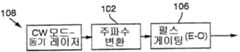
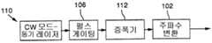
도 6은 본 발명에 따른 링크 절단을 달성하는데 바람직한 초단 레이저 펄스의 버스트를 생성하기 위해 CW 모드-동기 레이저(64)를 포함하는 간단한 레이저 시스템(60)의 바람직한 실시예를 도시하고 있다. 대략 200 ㎚로부터 1320 ㎚까지의 바람직한 레이저 파장은 Nd:YAG, Nd:YLF, Nd:YVO4, Yb:YAG, 또는 Ti:Sapphire 레이저(64)로부터 1.3, 1.064, 또는 1.047, 1.03 내지 1.05, 0.75 내지 0.85 ㎛ 또는 그것들의 제 2, 제 3, 제 4 또는 제 5 고조파를 포함하지만, 그것들로 제한되지는 않는다. 다른 적절한 파장에서 방출하는 레이저는 상업적으로 이용가능하고 또한 사용될 수 있다는 것을 당업자라면 알 것이다.Figure 6 illustrates a preferred embodiment of a
레이저 시스템(60)은, 주파수 배가 소자(frequency doubling element)가 고조파 변환을 제거하기 위해서 제거될 수 있기 때문에, 여기서는 단순히 일예로서 제 2의 고조파 (532 ㎚) Nd:YAG 레이저(64)로 모델링된다. Nd:YAG 또는 다른 고체-상태 레이저(64)는 바람직하게는 레이저 다이오드(70)나 레이저 다이오드-펌핑된 고체-상태 레이저에 의해서 펌핑되고, 그것의 방출은 렌즈 소자(74)에 의해서 레이저 공진기(82)에 집속된다. 레이저 공진기(82)는 짧은 흡수 길이를 바람직하게 갖는 레이선트(lasant)(84)와, 광학 축(90)을 따라 집속/폴딩 미러(76 및 78) 사이에 위치하는 Q-스위치(86)를 바람직하게 포함한다. 미러(78)는 광을 미러(76)와, 레이저(64)를 모드 동기시키기 위한 반도체 포화가능 흡수 미러 디바이스(92)에 반사한다. 미러(76)는 광을 미러(78)와, 광학 축(98)을 따라 공진기 출력(96)을 전파하는 부분적으로 반사성인 출력 커플러(94)에 반사한다. 고조파 변환 2배기(102)는 레이저 빔 주파수를 제 2 고조파 레이저 출력(104)으로 변환하기 위해서 공진기(82)에 외부적으로 위치되는 것이 바람직하다. UV로의 고조파 변환이 사용되는 경우에, 광학 게이트나 편광 상태 변환기 및 편광기와 같은 E-O 디바이스(106)는 고조파 변환 장치의 앞에 위치한다는 것을 당업자라면 알 것이다. 초단 레이저 펄스 폭과 그로 인한 더 높은 레이저 강도로 인해서, 더 높은 레이저 주파수 변환 효율이 쉽게 달성될 수 있다는 것을 당업자라면 알 것이다.The
Nd:YAG(532 ㎚, 355 ㎚, 266 ㎚); Nd:YLF(524 ㎚, 349 ㎚, 262 ㎚)의 제 2, 제 3, 또는 제 4 고조파 중 임의의 고조파나, Ti:Sapphire(375 내지 425 ㎚)의 제 2 고조파가 널리 알려진 적절한 고조파 변환 기술을 사용하여 특정 타입의 링크(22)를 바람직하게 처리하는데 사용될 수 있다는 것을 당업자라면 알 것이다. 고조파 변환 처리는 V. G. 드미트리브(V. G. Dmitriev) 등의 "Handbook of Nonlinear Optical Crystals"(Springer-Verlag, New York, 1991 ISBN 3-540-53547-0)의 138 내지 141쪽에 설명되어 있다.Nd: YAG (532 nm, 355 nm, 266 nm); Any harmonic of any of the second, third, or fourth harmonics of Nd: YLF (524 nm, 349 nm, 262 nm), or the second harmonic of Ti: Sapphire (375-425 nm), is a suitable harmonic conversion technique. It will be appreciated by those skilled in the art that the present invention can be used to desirably handle a particular type of
예시적인 초고속 Nd:YAG 또는 Nd:YLF 레이저(64)는 스위스의 취리히에 있는 Time-Bandwidth
또 다른 예시적인 레이저(64)는 750 내지 850 ㎚와 같이 근적외선(near IR) 범위 내의 레이저 파장을 갖는 모드-동기된 Ti-Sapphire 초단 펄스 레이저일 수 있다. 스펙트럼 물리학은 MAI TAITM으로 지칭되는 Ti-Sapphire 초고속 레이저를 만드 는데, 상기 MAI TAITM은 80 MHz의 반복 속도로 750 내지 850 ㎚ 범위에서 1W의 전력으로 100 fs의 펄스 폭을 갖는 초단 펄스(52)를 제공한다. 이러한 레이저(64)는 다이오드-펌핑되고 주파수-2배된 고체-상태 녹색 YAG 레이저(5W 또는 10W)에 의해서 펌핑된다.Another
도 7은 본 발명을 사용하기 위한 레이저 시스템(108)에 대한 간단한 대안적인 구성의 개략적인 도면을 도시한다. 고조파적으로 변환된 녹색 및 더 긴 파장 광에 대해서, E-O 디바이스(106)는 고조파 변환 변환기(102) 이후에 위치하는 것이 바람직하다는 것을 당업자라면 알 것이다.7 shows a schematic diagram of a simple alternative arrangement for a
도 8은 제 2 공진기나 증폭기(112)를 사용하는 레이저 시스템(110)에 대한 또 다른 간단한 대안적인 구성의 개략적인 도면을 도시한다.8 shows a schematic diagram of another simple alternative arrangement for a
(파장에 상관없이)레이저 출력(104)은 빔 경로(120)를 따라 위치해 있는 다양한 종래의 광학 소자(116 및 118)에 의해서 조작처리될 수 있다. 소자(116 및 118)는 유용한 전파 특징을 갖는 빔을 생성하도록 레이저 출력(104)을 조준(collimate)하기 위해서 빔 확장기나 다른 레이저 광학 소자를 포함할 수 있다. 하나 이상의 빔 반사 미러(122, 124, 126 및 128)는 선택적으로 사용되고, 원하는 레이저 파장에서 크게 반사적이지만, 사용되지 않는 파장에서는 매우 투과적이므로, 원하는 레이저 파장만이 링크 구조(36)에 도달할 것이다. 집속 렌즈(130)는 직경에 있어 2 ㎛ 보다 작거나 파장에 따라 더 작은 것이 바람직한 집속된 스폿 크기(40)를 생성하기 위해서 조준된 펄스형의 레이저 시스템 출력(140)을 집속시키 는 F1, F2, 또는 F3 단일 소자 또는 다중소자 렌즈 시스템을 바람직하게 사용한다.The laser output 104 (regardless of wavelength) may be manipulated by various conventional
바람직한 빔 위치지정 시스템(62)은 오버벡크(Overbeck)의 미국 특허 제 4,532,402호에 상세하게 설명되어 있다. 빔 위치지정 시스템(62)은 레이저 제어기(160)를 사용하는 것이 바람직한데, 상기 레이저 제어기(160)는 적어도 두 개의 플랫폼이나 스테이지(스택되거나 또는 분리된-축)를 제어하고, 레이저 시스템 출력(140)을 IC 디바이스나 워크피스(12) 상의 원하는 레이저 링크(22)에 겨냥하여 집속시키기 위해 반사기(122, 124, 126 및 128)와 협력하여 동작하다. 빔 위치지정 시스템(62)은 제공된 테스트나 설계 데이터에 기초하여 독특한 링크-절단 동작을 실행하도록 동일하거나 다른 워크피스(12) 상에 있는 링크(22) 사이에서의 신속한 이동을 허용한다.Preferred
위치 데이터는 링크(22)를 제거하기 위해 레이저 시스템 출력(140)의 초단 펄스(52)의 한 버스트(50)를 링크 구조(36)에 겨냥하도록 집속된 레이저 스폿(38)을 워크피스(12) 상으로 유도한다. 레이저 시스템(60)은 임의의 링크(22) 상에서 빔 위치지정 시스템(62)을 정지시키지 않고도 초단 레이저 펄스(52)의 단일 버스트(50)로 진행 중에 각각의 링크(22)를 바람직하게 절단함으로써, 높은 작업처리량이 유지된다. 버스트(50)는 500 ㎱ 보다 작기 때문에, 각각의 버스트(50)는 위치지정 시스템(62)에 의해서 단일 다중-나노세컨드 펄스와 같이 처리된다.The position data includes a
레이저 제어기(160)에는 링크 구조(36)의 특징에 따라 펄스(52)의 원하는 에너지 및 펄스 폭, 펄스(52)의 수, 및/또는 버스트(50)의 형태 및 지속기간에 관한 명령이 제공된다. 레이저 제어기(160)는 방사 빔 위치 및 방출 조정 시스템에 대한 코넥크니(Konecny)의 미국 특허 제 5,453,594호에서 설명된 바와 같이 레이저 시스템(60)의 발사를 플랫폼의 움직임에 맞추는 타이밍 데이터에 의해 좌우될 수 있다. 선택적으로, 레이저 제어기(160)는 폭켈 셀이나 음향-광학 디바이스(106)를 통한 레이저 에너지의 가외의 구멍의 조정에 사용될 수 있거나 Q-스위치(86)나 E-O 디바이스(106)를 제어하는 하나 이상의 부제어기(164)에 선택적으로 명령을 내릴 수 있다. 빔 위치지정 시스템(62)은 본 출원의 양수인에게 양도되어진 커틀러(Cutler) 등의 미국 특허 제 5,751,585호에 설명된 개선점 또는 빔 위치지정기를 선택적으로나 추가적으로 사용할 수 있다는 것을 당업자는 인식할 것이다. 다른 고정된 헤드, 검류계나, 압전적으로 또는 음성 코일로 제어되는 미러나, 선형 모터 구동식의 종래 위치지정 시스템과 같은 고속의 위치지정 헤드, 또는 오리건주의 포틀랜드에 있는 일렉트로 사이언티픽 인더스트리스, 인코포레이티드(ESI) 사에서 제작된 9300 또는 9000 모델 시리즈에서 사용되는 것들이 또한 사용될 수 있다.The
본 발명의 기본적인 원리에서 벗어나지 않으면서 본 발명에 대해 위에 설명된 실시예의 상세사항에 대한 많은 변형이 이루어질 수 있다는 것이 당업자들에게 명백해질 것이다. 그러므로, 본 발명의 범위는 다음의 청구항들에 의해서만 결정될 수 있다.It will be apparent to those skilled in the art that many modifications may be made to the details of the embodiments described above with respect to the present invention without departing from the basic principles thereof. Therefore, the scope of the invention may be determined only by the following claims.
상술된 바와 같이, 본 발명은 메모리 또는 다른 IC 링크의 레이저 처리에 관한 것으로, 특히, IC 링크를 절단하기 위해서 초단 펄스 폭을 가진 레이저 펄스의 버스트를 사용하는 레이저 시스템 및 방법에 이용가능하다.As mentioned above, the present invention relates to laser processing of memory or other IC links, and in particular, is applicable to laser systems and methods that use bursts of laser pulses with ultra short pulse widths to cut the IC links.
Claims (95)
Translated fromKorean


Applications Claiming Priority (4)
| Application Number | Priority Date | Filing Date | Title |
|---|---|---|---|
| US17533700P | 2000-01-10 | 2000-01-10 | |
| US60/175,337 | 2000-01-10 | ||
| US22353300P | 2000-08-04 | 2000-08-04 | |
| US60/223,533 | 2000-08-04 |
Related Child Applications (1)
| Application Number | Title | Priority Date | Filing Date |
|---|---|---|---|
| KR1020077006621ADivisionKR100850262B1 (en) | 2000-01-10 | 2001-01-09 | Laser system and method for processing a memory link with a burst of laser pulses having ultrashort pulse widths |
Publications (2)
| Publication Number | Publication Date |
|---|---|
| KR20020070332A KR20020070332A (en) | 2002-09-05 |
| KR100830128B1true KR100830128B1 (en) | 2008-05-20 |
Family
ID=26871111
Family Applications (2)
| Application Number | Title | Priority Date | Filing Date |
|---|---|---|---|
| KR1020077006621AExpired - Fee RelatedKR100850262B1 (en) | 2000-01-10 | 2001-01-09 | Laser system and method for processing a memory link with a burst of laser pulses having ultrashort pulse widths |
| KR1020027008432AExpired - Fee RelatedKR100830128B1 (en) | 2000-01-10 | 2001-01-09 | Laser system and method for processing memory links with bursts of laser pulses with very short pulse widths |
Family Applications Before (1)
| Application Number | Title | Priority Date | Filing Date |
|---|---|---|---|
| KR1020077006621AExpired - Fee RelatedKR100850262B1 (en) | 2000-01-10 | 2001-01-09 | Laser system and method for processing a memory link with a burst of laser pulses having ultrashort pulse widths |
Country Status (9)
| Country | Link |
|---|---|
| US (1) | US6574250B2 (en) |
| EP (1) | EP1247297A2 (en) |
| JP (1) | JP5123456B2 (en) |
| KR (2) | KR100850262B1 (en) |
| CN (1) | CN1276495C (en) |
| AU (1) | AU2001227764A1 (en) |
| CA (1) | CA2395960A1 (en) |
| TW (1) | TW476988B (en) |
| WO (1) | WO2001051243A2 (en) |
Families Citing this family (201)
| Publication number | Priority date | Publication date | Assignee | Title |
|---|---|---|---|---|
| US6822978B2 (en)* | 1999-05-27 | 2004-11-23 | Spectra Physics, Inc. | Remote UV laser system and methods of use |
| US6734387B2 (en)* | 1999-05-27 | 2004-05-11 | Spectra Physics Lasers, Inc. | Method and apparatus for micro-machining of articles that include polymeric materials |
| US6281471B1 (en)* | 1999-12-28 | 2001-08-28 | Gsi Lumonics, Inc. | Energy-efficient, laser-based method and system for processing target material |
| US20040134894A1 (en)* | 1999-12-28 | 2004-07-15 | Bo Gu | Laser-based system for memory link processing with picosecond lasers |
| US7838794B2 (en) | 1999-12-28 | 2010-11-23 | Gsi Group Corporation | Laser-based method and system for removing one or more target link structures |
| US7723642B2 (en)* | 1999-12-28 | 2010-05-25 | Gsi Group Corporation | Laser-based system for memory link processing with picosecond lasers |
| US20030222324A1 (en)* | 2000-01-10 | 2003-12-04 | Yunlong Sun | Laser systems for passivation or link processing with a set of laser pulses |
| US6887804B2 (en) | 2000-01-10 | 2005-05-03 | Electro Scientific Industries, Inc. | Passivation processing over a memory link |
| US20060141681A1 (en)* | 2000-01-10 | 2006-06-29 | Yunlong Sun | Processing a memory link with a set of at least two laser pulses |
| US7671295B2 (en) | 2000-01-10 | 2010-03-02 | Electro Scientific Industries, Inc. | Processing a memory link with a set of at least two laser pulses |
| JP2002040627A (en)* | 2000-07-24 | 2002-02-06 | Nec Corp | Method for correcting laser pattern and apparatus for correcting the same |
| US8497450B2 (en)* | 2001-02-16 | 2013-07-30 | Electro Scientific Industries, Inc. | On-the fly laser beam path dithering for enhancing throughput |
| US7027155B2 (en)* | 2001-03-29 | 2006-04-11 | Gsi Lumonics Corporation | Methods and systems for precisely relatively positioning a waist of a pulsed laser beam and method and system for controlling energy delivered to a target structure |
| US20070173075A1 (en)* | 2001-03-29 | 2007-07-26 | Joohan Lee | Laser-based method and system for processing a multi-material device having conductive link structures |
| US7563695B2 (en)* | 2002-03-27 | 2009-07-21 | Gsi Group Corporation | Method and system for high-speed precise laser trimming and scan lens for use therein |
| US6951995B2 (en) | 2002-03-27 | 2005-10-04 | Gsi Lumonics Corp. | Method and system for high-speed, precise micromachining an array of devices |
| JP2004200221A (en)* | 2002-12-16 | 2004-07-15 | Toray Eng Co Ltd | Laser marking method and device thereof |
| US6979798B2 (en)* | 2003-03-07 | 2005-12-27 | Gsi Lumonics Corporation | Laser system and method for material processing with ultra fast lasers |
| US7361171B2 (en) | 2003-05-20 | 2008-04-22 | Raydiance, Inc. | Man-portable optical ablation system |
| US7113327B2 (en)* | 2003-06-27 | 2006-09-26 | Imra America, Inc. | High power fiber chirped pulse amplification system utilizing telecom-type components |
| US6947454B2 (en)* | 2003-06-30 | 2005-09-20 | Electro Scientific Industries, Inc. | Laser pulse picking employing controlled AOM loading |
| US7616669B2 (en)* | 2003-06-30 | 2009-11-10 | Electro Scientific Industries, Inc. | High energy pulse suppression method |
| US7115514B2 (en)* | 2003-10-02 | 2006-10-03 | Raydiance, Inc. | Semiconductor manufacturing using optical ablation |
| US9022037B2 (en) | 2003-08-11 | 2015-05-05 | Raydiance, Inc. | Laser ablation method and apparatus having a feedback loop and control unit |
| US8921733B2 (en) | 2003-08-11 | 2014-12-30 | Raydiance, Inc. | Methods and systems for trimming circuits |
| US8173929B1 (en)* | 2003-08-11 | 2012-05-08 | Raydiance, Inc. | Methods and systems for trimming circuits |
| US7367969B2 (en)* | 2003-08-11 | 2008-05-06 | Raydiance, Inc. | Ablative material removal with a preset removal rate or volume or depth |
| KR101123911B1 (en)* | 2003-08-19 | 2012-03-23 | 일렉트로 싸이언티픽 인더스트리이즈 인코포레이티드 | Methods of and laser systems for link processing using laser pulses with specially tailored power profiles |
| KR101188356B1 (en)* | 2003-12-02 | 2012-10-08 | 가부시키가이샤 한도오따이 에네루기 켄큐쇼 | Laser irradiation apparatus, laser irradiation method, and method for manufacturing semiconductor device |
| EP1547719A3 (en)* | 2003-12-26 | 2009-01-28 | Semiconductor Energy Laboratory Co., Ltd. | Laser irradiation apparatus, laser irradiation method, and method for manufacturing crystalline semiconductor film |
| EP1553643A3 (en)* | 2003-12-26 | 2009-01-21 | Sel Semiconductor Energy Laboratory Co., Ltd. | Laser irradiation method and method for manufacturing crystalline semiconductor film |
| US7173212B1 (en)* | 2004-02-13 | 2007-02-06 | Semak Vladimir V | Method and apparatus for laser cutting and drilling of semiconductor materials and glass |
| US7057135B2 (en)* | 2004-03-04 | 2006-06-06 | Matsushita Electric Industrial, Co. Ltd. | Method of precise laser nanomachining with UV ultrafast laser pulses |
| US7491909B2 (en)* | 2004-03-31 | 2009-02-17 | Imra America, Inc. | Pulsed laser processing with controlled thermal and physical alterations |
| US7486705B2 (en) | 2004-03-31 | 2009-02-03 | Imra America, Inc. | Femtosecond laser processing system with process parameters, controls and feedback |
| US7139294B2 (en)* | 2004-05-14 | 2006-11-21 | Electro Scientific Industries, Inc. | Multi-output harmonic laser and methods employing same |
| US7804043B2 (en)* | 2004-06-15 | 2010-09-28 | Laserfacturing Inc. | Method and apparatus for dicing of thin and ultra thin semiconductor wafer using ultrafast pulse laser |
| US7633034B2 (en)* | 2004-06-18 | 2009-12-15 | Electro Scientific Industries, Inc. | Semiconductor structure processing using multiple laser beam spots overlapping lengthwise on a structure |
| US7629234B2 (en)* | 2004-06-18 | 2009-12-08 | Electro Scientific Industries, Inc. | Semiconductor structure processing using multiple laterally spaced laser beam spots with joint velocity profiling |
| US7935941B2 (en)* | 2004-06-18 | 2011-05-03 | Electro Scientific Industries, Inc. | Semiconductor structure processing using multiple laser beam spots spaced on-axis on non-adjacent structures |
| US7687740B2 (en)* | 2004-06-18 | 2010-03-30 | Electro Scientific Industries, Inc. | Semiconductor structure processing using multiple laterally spaced laser beam spots delivering multiple blows |
| US7435927B2 (en)* | 2004-06-18 | 2008-10-14 | Electron Scientific Industries, Inc. | Semiconductor link processing using multiple laterally spaced laser beam spots with on-axis offset |
| US7923306B2 (en)* | 2004-06-18 | 2011-04-12 | Electro Scientific Industries, Inc. | Semiconductor structure processing using multiple laser beam spots |
| US8383982B2 (en)* | 2004-06-18 | 2013-02-26 | Electro Scientific Industries, Inc. | Methods and systems for semiconductor structure processing using multiple laser beam spots |
| US8148211B2 (en)* | 2004-06-18 | 2012-04-03 | Electro Scientific Industries, Inc. | Semiconductor structure processing using multiple laser beam spots spaced on-axis delivered simultaneously |
| US8137340B2 (en)* | 2004-06-23 | 2012-03-20 | Applied Harmonics Corporation | Apparatus and method for soft tissue ablation employing high power diode-pumped laser |
| US20060000814A1 (en)* | 2004-06-30 | 2006-01-05 | Bo Gu | Laser-based method and system for processing targeted surface material and article produced thereby |
| JP2006032419A (en)* | 2004-07-12 | 2006-02-02 | Disco Abrasive Syst Ltd | Wafer laser processing method |
| US7902002B2 (en)* | 2004-07-30 | 2011-03-08 | Semiconductor Energy Laboratory Co., Ltd. | Semiconductor device |
| US20060032841A1 (en)* | 2004-08-10 | 2006-02-16 | Tan Kee C | Forming features in printhead components |
| JP4649927B2 (en)* | 2004-09-24 | 2011-03-16 | アイシン精機株式会社 | Laser-induced modification processing apparatus and method |
| US20060114948A1 (en)* | 2004-11-29 | 2006-06-01 | Lo Ho W | Workpiece processing system using a common imaged optical assembly to shape the spatial distributions of light energy of multiple laser beams |
| US7289549B2 (en)* | 2004-12-09 | 2007-10-30 | Electro Scientific Industries, Inc. | Lasers for synchronized pulse shape tailoring |
| US20060128073A1 (en)* | 2004-12-09 | 2006-06-15 | Yunlong Sun | Multiple-wavelength laser micromachining of semiconductor devices |
| WO2006072183A2 (en)* | 2005-01-10 | 2006-07-13 | Kresimir Franjic | LASER SYSTEM FOR GENERATION OF HIGH-POWER SUB-NANOSECOND PULSES WITH CONTROLLABLE WAVELENGTHS IN 2-15 um REGION |
| US20060191884A1 (en)* | 2005-01-21 | 2006-08-31 | Johnson Shepard D | High-speed, precise, laser-based material processing method and system |
| US7528342B2 (en)* | 2005-02-03 | 2009-05-05 | Laserfacturing, Inc. | Method and apparatus for via drilling and selective material removal using an ultrafast pulse laser |
| US8135050B1 (en) | 2005-07-19 | 2012-03-13 | Raydiance, Inc. | Automated polarization correction |
| BE1016782A3 (en)* | 2005-09-22 | 2007-06-05 | Laser Engineering Applic | METHOD FOR INTERNAL LASER MARKING IN TRANSPARENT AND LASER MATERIALS AND DEVICE USED FOR THE APPLICATION OF SAID METHOD |
| WO2007067643A2 (en)* | 2005-12-06 | 2007-06-14 | Electro Scientific Industries, Inc. | Simultaneously mode-locked, q-switched laser |
| CN101304712B (en)* | 2005-12-07 | 2011-06-29 | Sca卫生产品股份公司 | Method for manufacturing absorbent product |
| GB2434483A (en)* | 2006-01-20 | 2007-07-25 | Fianium Ltd | High-Power Short Optical Pulse Source |
| US8232687B2 (en) | 2006-04-26 | 2012-07-31 | Raydiance, Inc. | Intelligent laser interlock system |
| US9130344B2 (en)* | 2006-01-23 | 2015-09-08 | Raydiance, Inc. | Automated laser tuning |
| US7444049B1 (en) | 2006-01-23 | 2008-10-28 | Raydiance, Inc. | Pulse stretcher and compressor including a multi-pass Bragg grating |
| US8189971B1 (en) | 2006-01-23 | 2012-05-29 | Raydiance, Inc. | Dispersion compensation in a chirped pulse amplification system |
| US20070215575A1 (en)* | 2006-03-15 | 2007-09-20 | Bo Gu | Method and system for high-speed, precise, laser-based modification of one or more electrical elements |
| US7822347B1 (en) | 2006-03-28 | 2010-10-26 | Raydiance, Inc. | Active tuning of temporal dispersion in an ultrashort pulse laser system |
| US20080086118A1 (en)* | 2006-05-17 | 2008-04-10 | Applied Harmonics Corporation | Apparatus and method for diode-pumped laser ablation of soft tissue |
| US7605343B2 (en)* | 2006-05-24 | 2009-10-20 | Electro Scientific Industries, Inc. | Micromachining with short-pulsed, solid-state UV laser |
| US8084706B2 (en)* | 2006-07-20 | 2011-12-27 | Gsi Group Corporation | System and method for laser processing at non-constant velocities |
| JP2008147406A (en)* | 2006-12-08 | 2008-06-26 | Cyber Laser Kk | Laser integrated circuit correction method and apparatus |
| EP1990126B1 (en)* | 2007-05-08 | 2012-11-21 | Volvo Car Corporation | Method of laser cutting a painted or multilayered workpiece by means of a scanned laser beam |
| US8116341B2 (en)* | 2007-05-31 | 2012-02-14 | Electro Scientific Industries, Inc. | Multiple laser wavelength and pulse width process drilling |
| US20090004368A1 (en)* | 2007-06-29 | 2009-01-01 | Weyerhaeuser Co. | Systems and methods for curing a deposited layer on a substrate |
| US7903326B2 (en) | 2007-11-30 | 2011-03-08 | Radiance, Inc. | Static phase mask for high-order spectral phase control in a hybrid chirped pulse amplifier system |
| US20090141750A1 (en)* | 2007-12-03 | 2009-06-04 | Electro Scientific Industries, Inc. | Systems and methods for link processing with ultrafast and nanosecond laser pulses |
| GB2458475B (en)* | 2008-03-18 | 2011-10-26 | Xsil Technology Ltd | Processing of multilayer semiconductor wafers |
| US20090246530A1 (en)* | 2008-03-27 | 2009-10-01 | Imra America, Inc. | Method For Fabricating Thin Films |
| US20090246413A1 (en)* | 2008-03-27 | 2009-10-01 | Imra America, Inc. | Method for fabricating thin films |
| US7982160B2 (en) | 2008-03-31 | 2011-07-19 | Electro Scientific Industries, Inc. | Photonic clock stabilized laser comb processing |
| US8178818B2 (en)* | 2008-03-31 | 2012-05-15 | Electro Scientific Industries, Inc. | Photonic milling using dynamic beam arrays |
| US8526473B2 (en)* | 2008-03-31 | 2013-09-03 | Electro Scientific Industries | Methods and systems for dynamically generating tailored laser pulses |
| US8476552B2 (en)* | 2008-03-31 | 2013-07-02 | Electro Scientific Industries, Inc. | Laser systems and methods using triangular-shaped tailored laser pulses for selected target classes |
| US8598490B2 (en) | 2008-03-31 | 2013-12-03 | Electro Scientific Industries, Inc. | Methods and systems for laser processing a workpiece using a plurality of tailored laser pulse shapes |
| US20090289382A1 (en)* | 2008-05-22 | 2009-11-26 | Raydiance, Inc. | System and method for modifying characteristics of a contact lens utilizing an ultra-short pulsed laser |
| US8125704B2 (en) | 2008-08-18 | 2012-02-28 | Raydiance, Inc. | Systems and methods for controlling a pulsed laser by combining laser signals |
| US8309885B2 (en)* | 2009-01-15 | 2012-11-13 | Electro Scientific Industries, Inc. | Pulse temporal programmable ultrafast burst mode laser for micromachining |
| US8246714B2 (en)* | 2009-01-30 | 2012-08-21 | Imra America, Inc. | Production of metal and metal-alloy nanoparticles with high repetition rate ultrafast pulsed laser ablation in liquids |
| JP2010232650A (en)* | 2009-03-04 | 2010-10-14 | Omron Corp | Laser light source device, laser processing device, control device of laser light source device, and method of controlling laser light source device |
| US10307862B2 (en)* | 2009-03-27 | 2019-06-04 | Electro Scientific Industries, Inc | Laser micromachining with tailored bursts of short laser pulses |
| JP2010258120A (en)* | 2009-04-23 | 2010-11-11 | Fujifilm Corp | Ultrashort pulse light source and two-photon absorption recording medium recording apparatus having the same |
| KR20120113245A (en)* | 2009-12-30 | 2012-10-12 | 지에스아이 그룹 코포레이션 | Link processing with high speed beam deflection |
| US8540173B2 (en)* | 2010-02-10 | 2013-09-24 | Imra America, Inc. | Production of fine particles of functional ceramic by using pulsed laser |
| US20110192450A1 (en)* | 2010-02-10 | 2011-08-11 | Bing Liu | Method for producing nanoparticle solutions based on pulsed laser ablation for fabrication of thin film solar cells |
| US8858676B2 (en)* | 2010-02-10 | 2014-10-14 | Imra America, Inc. | Nanoparticle production in liquid with multiple-pulse ultrafast laser ablation |
| US8642448B2 (en) | 2010-06-22 | 2014-02-04 | Applied Materials, Inc. | Wafer dicing using femtosecond-based laser and plasma etch |
| US8884184B2 (en) | 2010-08-12 | 2014-11-11 | Raydiance, Inc. | Polymer tubing laser micromachining |
| KR20140018183A (en) | 2010-09-16 | 2014-02-12 | 레이디안스, 아이엔씨. | Laser based processing of layered materials |
| DE102011000768B4 (en)* | 2011-02-16 | 2016-08-18 | Ewag Ag | Laser processing method and laser processing apparatus with switchable laser arrangement |
| US8759197B2 (en) | 2011-06-15 | 2014-06-24 | Applied Materials, Inc. | Multi-step and asymmetrically shaped laser beam scribing |
| US8507363B2 (en) | 2011-06-15 | 2013-08-13 | Applied Materials, Inc. | Laser and plasma etch wafer dicing using water-soluble die attach film |
| US9126285B2 (en) | 2011-06-15 | 2015-09-08 | Applied Materials, Inc. | Laser and plasma etch wafer dicing using physically-removable mask |
| US8703581B2 (en) | 2011-06-15 | 2014-04-22 | Applied Materials, Inc. | Water soluble mask for substrate dicing by laser and plasma etch |
| US8557683B2 (en) | 2011-06-15 | 2013-10-15 | Applied Materials, Inc. | Multi-step and asymmetrically shaped laser beam scribing |
| US8557682B2 (en) | 2011-06-15 | 2013-10-15 | Applied Materials, Inc. | Multi-layer mask for substrate dicing by laser and plasma etch |
| US9029242B2 (en) | 2011-06-15 | 2015-05-12 | Applied Materials, Inc. | Damage isolation by shaped beam delivery in laser scribing process |
| US8912077B2 (en) | 2011-06-15 | 2014-12-16 | Applied Materials, Inc. | Hybrid laser and plasma etch wafer dicing using substrate carrier |
| US9129904B2 (en) | 2011-06-15 | 2015-09-08 | Applied Materials, Inc. | Wafer dicing using pulse train laser with multiple-pulse bursts and plasma etch |
| US8598016B2 (en) | 2011-06-15 | 2013-12-03 | Applied Materials, Inc. | In-situ deposited mask layer for device singulation by laser scribing and plasma etch |
| KR102138223B1 (en) | 2011-07-05 | 2020-07-28 | 일렉트로 싸이언티픽 인더스트리이즈 인코포레이티드 | Systems and methods for providing temperature stability of acousto-optic beam deflectors and acousto-optic modulators during use |
| US8951819B2 (en) | 2011-07-11 | 2015-02-10 | Applied Materials, Inc. | Wafer dicing using hybrid split-beam laser scribing process with plasma etch |
| US9061373B2 (en)* | 2011-11-30 | 2015-06-23 | Medtronic, Inc. | Welding method including continuous wave welding and pulse welding for component of an implantable medical device |
| KR20140112498A (en) | 2011-12-07 | 2014-09-23 | 제너럴 아토믹스 | Methods and Systems for Use in Laser Machining |
| JP5789527B2 (en)* | 2012-01-18 | 2015-10-07 | 株式会社アマダホールディングス | Laser processing apparatus and laser oscillation control method |
| KR101333554B1 (en)* | 2012-03-21 | 2013-11-28 | 위아코퍼레이션 주식회사 | Method for tempered glass processing using the laser pulse temporal control |
| CN102605333B (en)* | 2012-03-28 | 2013-11-27 | 中国矿业大学 | Preparation method of tantalum oxide film with high laser damage threshold under high temperature environment |
| US8652940B2 (en) | 2012-04-10 | 2014-02-18 | Applied Materials, Inc. | Wafer dicing used hybrid multi-step laser scribing process with plasma etch |
| US8946057B2 (en) | 2012-04-24 | 2015-02-03 | Applied Materials, Inc. | Laser and plasma etch wafer dicing using UV-curable adhesive film |
| US8969177B2 (en) | 2012-06-29 | 2015-03-03 | Applied Materials, Inc. | Laser and plasma etch wafer dicing with a double sided UV-curable adhesive film |
| US9048309B2 (en) | 2012-07-10 | 2015-06-02 | Applied Materials, Inc. | Uniform masking for wafer dicing using laser and plasma etch |
| US8940619B2 (en) | 2012-07-13 | 2015-01-27 | Applied Materials, Inc. | Method of diced wafer transportation |
| US8859397B2 (en) | 2012-07-13 | 2014-10-14 | Applied Materials, Inc. | Method of coating water soluble mask for laser scribing and plasma etch |
| US8845854B2 (en) | 2012-07-13 | 2014-09-30 | Applied Materials, Inc. | Laser, plasma etch, and backside grind process for wafer dicing |
| US8993414B2 (en) | 2012-07-13 | 2015-03-31 | Applied Materials, Inc. | Laser scribing and plasma etch for high die break strength and clean sidewall |
| US8842358B2 (en) | 2012-08-01 | 2014-09-23 | Gentex Corporation | Apparatus, method, and process with laser induced channel edge |
| US9159574B2 (en) | 2012-08-27 | 2015-10-13 | Applied Materials, Inc. | Method of silicon etch for trench sidewall smoothing |
| US9252057B2 (en) | 2012-10-17 | 2016-02-02 | Applied Materials, Inc. | Laser and plasma etch wafer dicing with partial pre-curing of UV release dicing tape for film frame wafer application |
| US8975162B2 (en) | 2012-12-20 | 2015-03-10 | Applied Materials, Inc. | Wafer dicing from wafer backside |
| US9236305B2 (en) | 2013-01-25 | 2016-01-12 | Applied Materials, Inc. | Wafer dicing with etch chamber shield ring for film frame wafer applications |
| US8980726B2 (en) | 2013-01-25 | 2015-03-17 | Applied Materials, Inc. | Substrate dicing by laser ablation and plasma etch damage removal for ultra-thin wafers |
| TWI619165B (en) | 2013-03-14 | 2018-03-21 | 應用材料股份有限公司 | Multi-layer mask with non-light definable laser energy absorbing layer for substrate cutting by laser and plasma etching |
| US8883614B1 (en) | 2013-05-22 | 2014-11-11 | Applied Materials, Inc. | Wafer dicing with wide kerf by laser scribing and plasma etching hybrid approach |
| US9105710B2 (en) | 2013-08-30 | 2015-08-11 | Applied Materials, Inc. | Wafer dicing method for improving die packaging quality |
| US9224650B2 (en) | 2013-09-19 | 2015-12-29 | Applied Materials, Inc. | Wafer dicing from wafer backside and front side |
| US9460966B2 (en) | 2013-10-10 | 2016-10-04 | Applied Materials, Inc. | Method and apparatus for dicing wafers having thick passivation polymer layer |
| US9041198B2 (en) | 2013-10-22 | 2015-05-26 | Applied Materials, Inc. | Maskless hybrid laser scribing and plasma etching wafer dicing process |
| US9312177B2 (en) | 2013-12-06 | 2016-04-12 | Applied Materials, Inc. | Screen print mask for laser scribe and plasma etch wafer dicing process |
| US9299614B2 (en) | 2013-12-10 | 2016-03-29 | Applied Materials, Inc. | Method and carrier for dicing a wafer |
| US9293304B2 (en) | 2013-12-17 | 2016-03-22 | Applied Materials, Inc. | Plasma thermal shield for heat dissipation in plasma chamber |
| US8927393B1 (en) | 2014-01-29 | 2015-01-06 | Applied Materials, Inc. | Water soluble mask formation by dry film vacuum lamination for laser and plasma dicing |
| US9012305B1 (en) | 2014-01-29 | 2015-04-21 | Applied Materials, Inc. | Wafer dicing using hybrid laser scribing and plasma etch approach with intermediate non-reactive post mask-opening clean |
| US9299611B2 (en) | 2014-01-29 | 2016-03-29 | Applied Materials, Inc. | Method of wafer dicing using hybrid laser scribing and plasma etch approach with mask plasma treatment for improved mask etch resistance |
| US9018079B1 (en) | 2014-01-29 | 2015-04-28 | Applied Materials, Inc. | Wafer dicing using hybrid laser scribing and plasma etch approach with intermediate reactive post mask-opening clean |
| US8991329B1 (en) | 2014-01-31 | 2015-03-31 | Applied Materials, Inc. | Wafer coating |
| US9236284B2 (en) | 2014-01-31 | 2016-01-12 | Applied Materials, Inc. | Cooled tape frame lift and low contact shadow ring for plasma heat isolation |
| US20150255349A1 (en) | 2014-03-07 | 2015-09-10 | JAMES Matthew HOLDEN | Approaches for cleaning a wafer during hybrid laser scribing and plasma etching wafer dicing processes |
| US9130030B1 (en) | 2014-03-07 | 2015-09-08 | Applied Materials, Inc. | Baking tool for improved wafer coating process |
| US9275902B2 (en) | 2014-03-26 | 2016-03-01 | Applied Materials, Inc. | Dicing processes for thin wafers with bumps on wafer backside |
| US9076860B1 (en) | 2014-04-04 | 2015-07-07 | Applied Materials, Inc. | Residue removal from singulated die sidewall |
| US8975163B1 (en) | 2014-04-10 | 2015-03-10 | Applied Materials, Inc. | Laser-dominated laser scribing and plasma etch hybrid wafer dicing |
| US8932939B1 (en) | 2014-04-14 | 2015-01-13 | Applied Materials, Inc. | Water soluble mask formation by dry film lamination |
| US8912078B1 (en) | 2014-04-16 | 2014-12-16 | Applied Materials, Inc. | Dicing wafers having solder bumps on wafer backside |
| US8999816B1 (en) | 2014-04-18 | 2015-04-07 | Applied Materials, Inc. | Pre-patterned dry laminate mask for wafer dicing processes |
| US9159621B1 (en) | 2014-04-29 | 2015-10-13 | Applied Materials, Inc. | Dicing tape protection for wafer dicing using laser scribe process |
| US8912075B1 (en) | 2014-04-29 | 2014-12-16 | Applied Materials, Inc. | Wafer edge warp supression for thin wafer supported by tape frame |
| US8980727B1 (en) | 2014-05-07 | 2015-03-17 | Applied Materials, Inc. | Substrate patterning using hybrid laser scribing and plasma etching processing schemes |
| US9112050B1 (en) | 2014-05-13 | 2015-08-18 | Applied Materials, Inc. | Dicing tape thermal management by wafer frame support ring cooling during plasma dicing |
| US9034771B1 (en) | 2014-05-23 | 2015-05-19 | Applied Materials, Inc. | Cooling pedestal for dicing tape thermal management during plasma dicing |
| US9130057B1 (en) | 2014-06-30 | 2015-09-08 | Applied Materials, Inc. | Hybrid dicing process using a blade and laser |
| US9165832B1 (en) | 2014-06-30 | 2015-10-20 | Applied Materials, Inc. | Method of die singulation using laser ablation and induction of internal defects with a laser |
| US9142459B1 (en) | 2014-06-30 | 2015-09-22 | Applied Materials, Inc. | Wafer dicing using hybrid laser scribing and plasma etch approach with mask application by vacuum lamination |
| US9093518B1 (en) | 2014-06-30 | 2015-07-28 | Applied Materials, Inc. | Singulation of wafers having wafer-level underfill |
| LT2965853T (en) | 2014-07-09 | 2016-11-25 | High Q Laser Gmbh | Processing of material using elongated laser beams |
| US9349648B2 (en) | 2014-07-22 | 2016-05-24 | Applied Materials, Inc. | Hybrid wafer dicing approach using a rectangular shaped two-dimensional top hat laser beam profile or a linear shaped one-dimensional top hat laser beam profile laser scribing process and plasma etch process |
| US9117868B1 (en) | 2014-08-12 | 2015-08-25 | Applied Materials, Inc. | Bipolar electrostatic chuck for dicing tape thermal management during plasma dicing |
| US9196498B1 (en) | 2014-08-12 | 2015-11-24 | Applied Materials, Inc. | Stationary actively-cooled shadow ring for heat dissipation in plasma chamber |
| US9281244B1 (en) | 2014-09-18 | 2016-03-08 | Applied Materials, Inc. | Hybrid wafer dicing approach using an adaptive optics-controlled laser scribing process and plasma etch process |
| US9177861B1 (en) | 2014-09-19 | 2015-11-03 | Applied Materials, Inc. | Hybrid wafer dicing approach using laser scribing process based on an elliptical laser beam profile or a spatio-temporal controlled laser beam profile |
| US11195756B2 (en) | 2014-09-19 | 2021-12-07 | Applied Materials, Inc. | Proximity contact cover ring for plasma dicing |
| US9196536B1 (en) | 2014-09-25 | 2015-11-24 | Applied Materials, Inc. | Hybrid wafer dicing approach using a phase modulated laser beam profile laser scribing process and plasma etch process |
| US9130056B1 (en) | 2014-10-03 | 2015-09-08 | Applied Materials, Inc. | Bi-layer wafer-level underfill mask for wafer dicing and approaches for performing wafer dicing |
| US9245803B1 (en) | 2014-10-17 | 2016-01-26 | Applied Materials, Inc. | Hybrid wafer dicing approach using a bessel beam shaper laser scribing process and plasma etch process |
| US10692765B2 (en) | 2014-11-07 | 2020-06-23 | Applied Materials, Inc. | Transfer arm for film frame substrate handling during plasma singulation of wafers |
| US9355907B1 (en) | 2015-01-05 | 2016-05-31 | Applied Materials, Inc. | Hybrid wafer dicing approach using a line shaped laser beam profile laser scribing process and plasma etch process |
| US9330977B1 (en) | 2015-01-05 | 2016-05-03 | Applied Materials, Inc. | Hybrid wafer dicing approach using a galvo scanner and linear stage hybrid motion laser scribing process and plasma etch process |
| US9159624B1 (en) | 2015-01-05 | 2015-10-13 | Applied Materials, Inc. | Vacuum lamination of polymeric dry films for wafer dicing using hybrid laser scribing and plasma etch approach |
| JP6464789B2 (en)* | 2015-02-10 | 2019-02-06 | オムロン株式会社 | Inspection apparatus, laser processing apparatus, and laser processing inspection method |
| US9601375B2 (en) | 2015-04-27 | 2017-03-21 | Applied Materials, Inc. | UV-cure pre-treatment of carrier film for wafer dicing using hybrid laser scribing and plasma etch approach |
| US9478455B1 (en) | 2015-06-12 | 2016-10-25 | Applied Materials, Inc. | Thermal pyrolytic graphite shadow ring assembly for heat dissipation in plasma chamber |
| US9721839B2 (en) | 2015-06-12 | 2017-08-01 | Applied Materials, Inc. | Etch-resistant water soluble mask for hybrid wafer dicing using laser scribing and plasma etch |
| US9972575B2 (en) | 2016-03-03 | 2018-05-15 | Applied Materials, Inc. | Hybrid wafer dicing approach using a split beam laser scribing process and plasma etch process |
| US9852997B2 (en) | 2016-03-25 | 2017-12-26 | Applied Materials, Inc. | Hybrid wafer dicing approach using a rotating beam laser scribing process and plasma etch process |
| JP6755707B2 (en)* | 2016-05-12 | 2020-09-16 | 株式会社ディスコ | Laser processing equipment |
| US9793132B1 (en) | 2016-05-13 | 2017-10-17 | Applied Materials, Inc. | Etch mask for hybrid laser scribing and plasma etch wafer singulation process |
| JP6770340B2 (en)* | 2016-05-30 | 2020-10-14 | 株式会社ディスコ | How to generate a wafer |
| CN106238907A (en)* | 2016-08-22 | 2016-12-21 | 大族激光科技产业集团股份有限公司 | The laser processing of LED wafer |
| JP6363680B2 (en)* | 2016-11-16 | 2018-07-25 | ファナック株式会社 | Laser equipment |
| US11158540B2 (en) | 2017-05-26 | 2021-10-26 | Applied Materials, Inc. | Light-absorbing mask for hybrid laser scribing and plasma etch wafer singulation process |
| US10363629B2 (en) | 2017-06-01 | 2019-07-30 | Applied Materials, Inc. | Mitigation of particle contamination for wafer dicing processes |
| US10535561B2 (en) | 2018-03-12 | 2020-01-14 | Applied Materials, Inc. | Hybrid wafer dicing approach using a multiple pass laser scribing process and plasma etch process |
| US11081855B2 (en)* | 2018-06-18 | 2021-08-03 | Coherent, Inc. | Laser-MOPA with burst-mode control |
| US11355394B2 (en) | 2018-09-13 | 2022-06-07 | Applied Materials, Inc. | Wafer dicing using hybrid laser scribing and plasma etch approach with intermediate breakthrough treatment |
| KR20250033309A (en)* | 2019-06-10 | 2025-03-07 | 일렉트로 싸이언티픽 인더스트리이즈 인코포레이티드 | Laser processing apparatus, methods of operating the same, and methods of processing workpieces using the same |
| US11011424B2 (en) | 2019-08-06 | 2021-05-18 | Applied Materials, Inc. | Hybrid wafer dicing approach using a spatially multi-focused laser beam laser scribing process and plasma etch process |
| US11342226B2 (en) | 2019-08-13 | 2022-05-24 | Applied Materials, Inc. | Hybrid wafer dicing approach using an actively-focused laser beam laser scribing process and plasma etch process |
| US10903121B1 (en) | 2019-08-14 | 2021-01-26 | Applied Materials, Inc. | Hybrid wafer dicing approach using a uniform rotating beam laser scribing process and plasma etch process |
| US11600492B2 (en) | 2019-12-10 | 2023-03-07 | Applied Materials, Inc. | Electrostatic chuck with reduced current leakage for hybrid laser scribing and plasma etch wafer singulation process |
| US11211247B2 (en) | 2020-01-30 | 2021-12-28 | Applied Materials, Inc. | Water soluble organic-inorganic hybrid mask formulations and their applications |
| JP7497670B2 (en)* | 2020-10-29 | 2024-06-11 | セイコーエプソン株式会社 | Manufacturing method of watch parts, and watch parts |
| CN112756808A (en)* | 2020-12-31 | 2021-05-07 | 天津爱旭太阳能科技有限公司 | Cutting method for reducing recombination loss of crystalline silicon solar cell |
Citations (3)
| Publication number | Priority date | Publication date | Assignee | Title |
|---|---|---|---|---|
| US5656186A (en) | 1994-04-08 | 1997-08-12 | The Regents Of The University Of Michigan | Method for controlling configuration of laser induced breakdown and ablation |
| US5720894A (en) | 1996-01-11 | 1998-02-24 | The Regents Of The University Of California | Ultrashort pulse high repetition rate laser system for biological tissue processing |
| US5725914A (en) | 1992-09-03 | 1998-03-10 | Deutsche Forschungsanstalt fuer Luft - und Raumfahrt e.V. | Process and apparatus for producing a functional structure of a semiconductor component |
Family Cites Families (33)
| Publication number | Priority date | Publication date | Assignee | Title |
|---|---|---|---|---|
| US4114018A (en) | 1976-09-30 | 1978-09-12 | Lasag Ag | Method for ablating metal workpieces with laser radiation |
| US4532402A (en)* | 1983-09-02 | 1985-07-30 | Xrl, Inc. | Method and apparatus for positioning a focused beam on an integrated circuit |
| JPS61290719A (en)* | 1985-06-19 | 1986-12-20 | Hitachi Ltd | Laser output control device |
| JPH0821623B2 (en)* | 1985-09-20 | 1996-03-04 | 株式会社日立製作所 | Laser processing method |
| US4646308A (en) | 1985-09-30 | 1987-02-24 | Spectra-Physics, Inc. | Synchronously pumped dye laser using ultrashort pump pulses |
| US4932031A (en) | 1987-12-04 | 1990-06-05 | Alfano Robert R | Chromium-doped foresterite laser system |
| US5034951A (en) | 1989-06-26 | 1991-07-23 | Cornell Research Foundation, Inc. | Femtosecond ultraviolet laser using ultra-thin beta barium borate |
| JPH03278489A (en)* | 1990-02-14 | 1991-12-10 | Nippon Koden Corp | Laser surgical operation device |
| US5042040A (en) | 1990-03-30 | 1991-08-20 | At&T Bell Laboratories | Amplitude noise reduction for optically pumped modelocked lasers |
| JP3150322B2 (en)* | 1990-05-18 | 2001-03-26 | 株式会社日立製作所 | Wiring cutting method by laser and laser processing device |
| US5175664A (en) | 1991-12-05 | 1992-12-29 | Diels Jean Claude | Discharge of lightning with ultrashort laser pulses |
| US5265114C1 (en) | 1992-09-10 | 2001-08-21 | Electro Scient Ind Inc | System and method for selectively laser processing a target structure of one or more materials of a multimaterial multilayer device |
| US5520679A (en) | 1992-12-03 | 1996-05-28 | Lasersight, Inc. | Ophthalmic surgery method using non-contact scanning laser |
| US5453594A (en)* | 1993-10-06 | 1995-09-26 | Electro Scientific Industries, Inc. | Radiation beam position and emission coordination system |
| US5611946A (en) | 1994-02-18 | 1997-03-18 | New Wave Research | Multi-wavelength laser system, probe station and laser cutter system using the same |
| US5558789A (en) | 1994-03-02 | 1996-09-24 | University Of Florida | Method of applying a laser beam creating micro-scale surface structures prior to deposition of film for increased adhesion |
| JP2526806B2 (en) | 1994-04-26 | 1996-08-21 | 日本電気株式会社 | Semiconductor laser and its operating method |
| US5513194A (en) | 1994-06-30 | 1996-04-30 | Massachusetts Institute Of Technology | Stretched-pulse fiber laser |
| US5539764A (en) | 1994-08-24 | 1996-07-23 | Jamar Technologies Co. | Laser generated X-ray source |
| US5742634A (en) | 1994-08-24 | 1998-04-21 | Imar Technology Co. | Picosecond laser |
| US5751585A (en) | 1995-03-20 | 1998-05-12 | Electro Scientific Industries, Inc. | High speed, high accuracy multi-stage tool positioning system |
| US5786560A (en) | 1995-03-31 | 1998-07-28 | Panasonic Technologies, Inc. | 3-dimensional micromachining with femtosecond laser pulses |
| US5627848A (en) | 1995-09-05 | 1997-05-06 | Imra America, Inc. | Apparatus for producing femtosecond and picosecond pulses from modelocked fiber lasers cladding pumped with broad area diode laser arrays |
| US5956354A (en) | 1996-06-06 | 1999-09-21 | The University Of Maryland Baltimore County | Dual media laser with mode locking |
| US5998759A (en) | 1996-12-24 | 1999-12-07 | General Scanning, Inc. | Laser processing |
| US6025256A (en) | 1997-01-06 | 2000-02-15 | Electro Scientific Industries, Inc. | Laser based method and system for integrated circuit repair or reconfiguration |
| US5848080A (en) | 1997-05-12 | 1998-12-08 | Dahm; Jonathan S. | Short pulsewidth high pulse repetition frequency laser |
| JPH11197863A (en)* | 1998-01-09 | 1999-07-27 | Nikon Corp | Laser processing equipment |
| US5953354A (en) | 1998-02-03 | 1999-09-14 | General Electric Co. | Laser resonator optical alignment |
| US5987049A (en) | 1998-04-24 | 1999-11-16 | Time-Bandwidth Products Ag | Mode locked solid-state laser pumped by a non-diffraction-limited pumping source and method for generating pulsed laser radiation by pumping with a non-diffraction-limited pumping beam |
| US6057180A (en)* | 1998-06-05 | 2000-05-02 | Electro Scientific Industries, Inc. | Method of severing electrically conductive links with ultraviolet laser output |
| US6281471B1 (en) | 1999-12-28 | 2001-08-28 | Gsi Lumonics, Inc. | Energy-efficient, laser-based method and system for processing target material |
| US6552301B2 (en) | 2000-01-25 | 2003-04-22 | Peter R. Herman | Burst-ultrafast laser machining method |
- 2001
- 2001-01-09AUAU2001227764Apatent/AU2001227764A1/ennot_activeAbandoned
- 2001-01-09KRKR1020077006621Apatent/KR100850262B1/ennot_activeExpired - Fee Related
- 2001-01-09CACA002395960Apatent/CA2395960A1/ennot_activeAbandoned
- 2001-01-09CNCNB018035868Apatent/CN1276495C/ennot_activeExpired - Fee Related
- 2001-01-09EPEP01901912Apatent/EP1247297A2/ennot_activeCeased
- 2001-01-09WOPCT/US2001/000711patent/WO2001051243A2/enactiveApplication Filing
- 2001-01-09USUS09/757,418patent/US6574250B2/ennot_activeExpired - Lifetime
- 2001-01-09KRKR1020027008432Apatent/KR100830128B1/ennot_activeExpired - Fee Related
- 2001-01-09JPJP2001551650Apatent/JP5123456B2/ennot_activeExpired - Fee Related
- 2001-02-05TWTW090100492Apatent/TW476988B/ennot_activeIP Right Cessation
Patent Citations (3)
| Publication number | Priority date | Publication date | Assignee | Title |
|---|---|---|---|---|
| US5725914A (en) | 1992-09-03 | 1998-03-10 | Deutsche Forschungsanstalt fuer Luft - und Raumfahrt e.V. | Process and apparatus for producing a functional structure of a semiconductor component |
| US5656186A (en) | 1994-04-08 | 1997-08-12 | The Regents Of The University Of Michigan | Method for controlling configuration of laser induced breakdown and ablation |
| US5720894A (en) | 1996-01-11 | 1998-02-24 | The Regents Of The University Of California | Ultrashort pulse high repetition rate laser system for biological tissue processing |
Also Published As
| Publication number | Publication date |
|---|---|
| CN1276495C (en) | 2006-09-20 |
| CN1394358A (en) | 2003-01-29 |
| US20020003130A1 (en) | 2002-01-10 |
| CA2395960A1 (en) | 2001-07-19 |
| WO2001051243A2 (en) | 2001-07-19 |
| WO2001051243A3 (en) | 2001-12-13 |
| JP2003519933A (en) | 2003-06-24 |
| TW476988B (en) | 2002-02-21 |
| KR100850262B1 (en) | 2008-08-04 |
| KR20070040849A (en) | 2007-04-17 |
| EP1247297A2 (en) | 2002-10-09 |
| AU2001227764A1 (en) | 2001-07-24 |
| JP5123456B2 (en) | 2013-01-23 |
| US6574250B2 (en) | 2003-06-03 |
| KR20020070332A (en) | 2002-09-05 |
Similar Documents
| Publication | Publication Date | Title |
|---|---|---|
| KR100830128B1 (en) | Laser system and method for processing memory links with bursts of laser pulses with very short pulse widths | |
| US7671295B2 (en) | Processing a memory link with a set of at least two laser pulses | |
| US6887804B2 (en) | Passivation processing over a memory link | |
| US8253066B2 (en) | Laser-based method and system for removing one or more target link structures | |
| KR101370156B1 (en) | Laser-based method and system for removing one or more target link structures | |
| JP2007508694A (en) | Laser-based system for memory link processing with picosecond lasers | |
| CA2535706A1 (en) | Generating sets of tailored laser pulses | |
| KR20040073958A (en) | Processing a memory link with a set of at least two laser pulses | |
| US20030222324A1 (en) | Laser systems for passivation or link processing with a set of laser pulses | |
| JP2011508670A (en) | System and method for link processing with ultrafast laser pulses and nanosecond laser pulses | |
| US20060141681A1 (en) | Processing a memory link with a set of at least two laser pulses | |
| CN1919520A (en) | Laser system and method for processing a memory link with in integrated circuit |
Legal Events
| Date | Code | Title | Description |
|---|---|---|---|
| PA0105 | International application | St.27 status event code:A-0-1-A10-A15-nap-PA0105 | |
| PG1501 | Laying open of application | St.27 status event code:A-1-1-Q10-Q12-nap-PG1501 | |
| A201 | Request for examination | ||
| P11-X000 | Amendment of application requested | St.27 status event code:A-2-2-P10-P11-nap-X000 | |
| P13-X000 | Application amended | St.27 status event code:A-2-2-P10-P13-nap-X000 | |
| PA0201 | Request for examination | St.27 status event code:A-1-2-D10-D11-exm-PA0201 | |
| E902 | Notification of reason for refusal | ||
| PE0902 | Notice of grounds for rejection | St.27 status event code:A-1-2-D10-D21-exm-PE0902 | |
| T11-X000 | Administrative time limit extension requested | St.27 status event code:U-3-3-T10-T11-oth-X000 | |
| T11-X000 | Administrative time limit extension requested | St.27 status event code:U-3-3-T10-T11-oth-X000 | |
| E14-X000 | Pre-grant third party observation filed | St.27 status event code:A-2-3-E10-E14-opp-X000 | |
| A107 | Divisional application of patent | ||
| P11-X000 | Amendment of application requested | St.27 status event code:A-2-2-P10-P11-nap-X000 | |
| P13-X000 | Application amended | St.27 status event code:A-2-2-P10-P13-nap-X000 | |
| PA0104 | Divisional application for international application | St.27 status event code:A-0-1-A10-A18-div-PA0104 St.27 status event code:A-0-1-A10-A16-div-PA0104 | |
| E801 | Decision on dismissal of amendment | ||
| T11-X000 | Administrative time limit extension requested | St.27 status event code:U-3-3-T10-T11-oth-X000 | |
| J301 | Trial decision | Free format text:TRIAL DECISION FOR APPEAL AGAINST DECISION TO DECLINE AMENDMENT REQUESTED 20071012 Effective date:20080130 | |
| PJ1301 | Trial decision | St.27 status event code:A-3-3-V10-V15-crt-PJ1301 Decision date:20080130 Appeal event data comment text:Appeal Kind Category : Appeal against decision to decline amendment, Appeal Ground Text : 2002 7008432 Appeal request date:20071012 Appellate body name:Patent Examination Board Decision authority category:Office appeal board Decision identifier:2007102000067 | |
| PS0901 | Examination by remand of revocation | St.27 status event code:A-6-3-E10-E12-rex-PS0901 | |
| S901 | Examination by remand of revocation | ||
| GRNO | Decision to grant (after opposition) | ||
| PS0701 | Decision of registration after remand of revocation | St.27 status event code:A-3-4-F10-F13-rex-PS0701 | |
| GRNT | Written decision to grant | ||
| PR0701 | Registration of establishment | St.27 status event code:A-2-4-F10-F11-exm-PR0701 | |
| PR1002 | Payment of registration fee | St.27 status event code:A-2-2-U10-U12-oth-PR1002 Fee payment year number:1 | |
| PG1601 | Publication of registration | St.27 status event code:A-4-4-Q10-Q13-nap-PG1601 | |
| PR1001 | Payment of annual fee | St.27 status event code:A-4-4-U10-U11-oth-PR1001 Fee payment year number:4 | |
| PR1001 | Payment of annual fee | St.27 status event code:A-4-4-U10-U11-oth-PR1001 Fee payment year number:5 | |
| FPAY | Annual fee payment | Payment date:20130424 Year of fee payment:6 | |
| PR1001 | Payment of annual fee | St.27 status event code:A-4-4-U10-U11-oth-PR1001 Fee payment year number:6 | |
| R18-X000 | Changes to party contact information recorded | St.27 status event code:A-5-5-R10-R18-oth-X000 | |
| FPAY | Annual fee payment | Payment date:20140424 Year of fee payment:7 | |
| PR1001 | Payment of annual fee | St.27 status event code:A-4-4-U10-U11-oth-PR1001 Fee payment year number:7 | |
| FPAY | Annual fee payment | Payment date:20150427 Year of fee payment:8 | |
| PR1001 | Payment of annual fee | St.27 status event code:A-4-4-U10-U11-oth-PR1001 Fee payment year number:8 | |
| FPAY | Annual fee payment | Payment date:20160426 Year of fee payment:9 | |
| PR1001 | Payment of annual fee | St.27 status event code:A-4-4-U10-U11-oth-PR1001 Fee payment year number:9 | |
| FPAY | Annual fee payment | Payment date:20170426 Year of fee payment:10 | |
| PR1001 | Payment of annual fee | St.27 status event code:A-4-4-U10-U11-oth-PR1001 Fee payment year number:10 | |
| R18-X000 | Changes to party contact information recorded | St.27 status event code:A-5-5-R10-R18-oth-X000 | |
| LAPS | Lapse due to unpaid annual fee | ||
| PC1903 | Unpaid annual fee | St.27 status event code:A-4-4-U10-U13-oth-PC1903 Not in force date:20180510 Payment event data comment text:Termination Category : DEFAULT_OF_REGISTRATION_FEE | |
| PC1903 | Unpaid annual fee | St.27 status event code:N-4-6-H10-H13-oth-PC1903 Ip right cessation event data comment text:Termination Category : DEFAULT_OF_REGISTRATION_FEE Not in force date:20180510 | |
| R18-X000 | Changes to party contact information recorded | St.27 status event code:A-5-5-R10-R18-oth-X000 |