KR100829746B1 - Plasma display device and manufacturing method thereof - Google Patents
Plasma display device and manufacturing method thereofDownload PDFInfo
- Publication number
- KR100829746B1 KR100829746B1KR1020060106997AKR20060106997AKR100829746B1KR 100829746 B1KR100829746 B1KR 100829746B1KR 1020060106997 AKR1020060106997 AKR 1020060106997AKR 20060106997 AKR20060106997 AKR 20060106997AKR 100829746 B1KR100829746 B1KR 100829746B1
- Authority
- KR
- South Korea
- Prior art keywords
- discharge
- substrate
- plasma display
- oxide film
- groove
- Prior art date
- Legal status (The legal status is an assumption and is not a legal conclusion. Google has not performed a legal analysis and makes no representation as to the accuracy of the status listed.)
- Expired - Fee Related
Links
Images


Classifications
- H—ELECTRICITY
- H01—ELECTRIC ELEMENTS
- H01J—ELECTRIC DISCHARGE TUBES OR DISCHARGE LAMPS
- H01J11/00—Gas-filled discharge tubes with alternating current induction of the discharge, e.g. alternating current plasma display panels [AC-PDP]; Gas-filled discharge tubes without any main electrode inside the vessel; Gas-filled discharge tubes with at least one main electrode outside the vessel
- H01J11/20—Constructional details
- H01J11/34—Vessels, containers or parts thereof, e.g. substrates
- H—ELECTRICITY
- H01—ELECTRIC ELEMENTS
- H01J—ELECTRIC DISCHARGE TUBES OR DISCHARGE LAMPS
- H01J11/00—Gas-filled discharge tubes with alternating current induction of the discharge, e.g. alternating current plasma display panels [AC-PDP]; Gas-filled discharge tubes without any main electrode inside the vessel; Gas-filled discharge tubes with at least one main electrode outside the vessel
- H01J11/10—AC-PDPs with at least one main electrode being out of contact with the plasma
- H01J11/16—AC-PDPs with at least one main electrode being out of contact with the plasma with main electrodes provided inside or on the side face of the spacers
- H—ELECTRICITY
- H01—ELECTRIC ELEMENTS
- H01J—ELECTRIC DISCHARGE TUBES OR DISCHARGE LAMPS
- H01J9/00—Apparatus or processes specially adapted for the manufacture, installation, removal, maintenance of electric discharge tubes, discharge lamps, or parts thereof; Recovery of material from discharge tubes or lamps
- H01J9/24—Manufacture or joining of vessels, leading-in conductors or bases
- H01J9/241—Manufacture or joining of vessels, leading-in conductors or bases the vessel being for a flat panel display
Landscapes
- Engineering & Computer Science (AREA)
- Physics & Mathematics (AREA)
- Plasma & Fusion (AREA)
- Manufacturing & Machinery (AREA)
- Gas-Filled Discharge Tubes (AREA)
Abstract
Translated fromKoreanDescription
Translated fromKorean도 1은 종래기술에 의한 플라즈마 디스플레이 장치의 분해 사시도이다.1 is an exploded perspective view of a plasma display device according to the prior art.
도 2는 본 발명의 제1 실시예에 따른 플라즈마 디스플레이 장치의 주요부를 도시한 분해 사시도이다.2 is an exploded perspective view showing the main part of the plasma display device according to the first embodiment of the present invention.
도 3은 도 2의 선을 따라 취한 수직 단면도이다.3 is a vertical cross-sectional view taken along the line of FIG. 2.
도 4는 도 2의 전극 배치구조를 도시한 사시도이다.4 is a perspective view illustrating the electrode arrangement structure of FIG. 2.
도 5는 도 2의 배면기판 측을 도시한 사시도이다.FIG. 5 is a perspective view illustrating the back substrate side of FIG. 2.
도 6a 내지 도 6j에는 도 2의 플라즈마 디스플레이 장치의 제조방법을 그 공정단계별로 도시한 수직 단면도들이다.6A through 6J are vertical cross-sectional views illustrating the method of manufacturing the plasma display device of FIG. 2 according to the process steps.
도 7은 본 발명의 제2 실시예에 따른 플라즈마 디스플레이 장치의 주요부를 도시한 분해 사시도이다.7 is an exploded perspective view showing the main part of the plasma display device according to the second embodiment of the present invention.
도 8은 도 7의 Ⅷ-Ⅷ 선을 따라 취한 수직 단면도이다.8 is a vertical cross-sectional view taken along the line VII-VII of FIG. 7.
도 9는 도 7의 전극 배치구조를 도시한 사시도이다.9 is a perspective view illustrating the electrode arrangement structure of FIG. 7.
<도면의 주요부분에 대한 부호의 설명><Description of the symbols for the main parts of the drawings>
110,210 : 전면기판111,211 : 제2 그루브110,210: Front substrate 111,211: Second groove
120,220 : 배면기판120`: 알루미늄 플레이트120,220: Back
121,221 : 제1 그루브122 : 산화피막121,221: first groove 122: oxide film
125,225 : 형광체130,230 : 격벽125,225 phosphor 130,230 partition wall
131,231 : 제1 방전전극131a,231a : 방전부131,231:
131b, 231b : 통전부132,232 : 제2 방전전극131b and 231b: energization part 132,232: second discharge electrode
132a,232a : 방전부132b,232b : 통전부132a, 232a: discharge
233 : 제3 방전전극233a : 방전부233:
233b ; 통전부 135,235 : 보호막233b; Current carrying part 135,235: Shield
160 : 구동회로부S : 방전공간160: drive circuit portion S: discharge space
W1 : 그루브 부분W2 : 그루브 사이 부분W1: groove portion W2: portion between grooves
PR : PR 마스크 OB : 산화방지용 마스크PR: PR Mask OB: Anti-oxidation Mask
본 발명은 가스방전을 이용하여 화상을 구현하는 플라즈마 디스플레이 장치 및 그 제조방법에 관한 것으로, 구성부품 및 조립공수가 감축되어 원가절감이 가능하며, 박형화 및 경량화에 유리한 플라즈마 디스플레이 장치 및 그 제조방법에 관한 것이다.The present invention relates to a plasma display device for realizing an image using gas discharge, and a method of manufacturing the same, and to reducing the cost by reducing component and assembly labor, and to a plasma display device and a method for manufacturing the same, which are advantageous for thinning and weight reduction. will be.
평판 디스플레이 장치로서 플라즈마 디스플레이 장치는 대화면을 가지면서도, 고화질, 초박형, 경량화 및 광시야각의 우수한 특성을 갖고 있으며, 다른 평판 디스플레이 장치에 비해 제조방법이 간단하고 대형화가 용이하여 차세대 대형 평판 디스플레이 장치로서 각광을 받고 있다.As a flat panel display device, the plasma display device has a large screen, high quality, ultra-thin, light weight, and wide viewing angle, and has a spotlight as a next-generation large flat panel display device because its manufacturing method is simpler and easier to enlarge than other flat panel display devices. Is getting.
도 1에는 종래기술에 따른 플라즈마 디스플레이 장치의 분해 사시도가 도시되어 있다. 도면을 참조하면, 일반적으로, 플라즈마 디스플레이 장치는 방전현상에 의해 영상이 구현되는 플라즈마 디스플레이 패널(30) 및 상기 플라즈마 디스플레이 패널(30)에 제어된 구동신호를 인가하기 위한 구동회로부(60)를 구비한다. 상기 플라즈마 디스플레이 패널(30)은 서로 마주보게 배치되어 있는 전면 및 배면 글라스 기판(10,20) 사이에 방전이 수행되는 복수의 방전셀들(미도시) 및 상기 방전셀들에 걸쳐서 배치되어 방전을 일으키는 방전전극들(미도시)을 구비하며, 상기 구동회로부(60)는 상기 방전전극들에 구동신호를 인가하기 위해, 다수의 구동IC 및 다수의 회로소자들이 탑재된 회로기판들을 포함한다. 상기 플라즈마 디스플레이 패널(30) 및 구동회로부(60)는 알루미늄 플레이트로 이루어진 샤시베이스(50)에 장착되어 지지된다. 보다 구체적으로, 상기 샤시베이스(50)는 그 전방 면을 통해 상기 플라즈마 디스플레이 패널(30)을 지지하며, 그 후방 면을 통해 상기 구동회로부(60)를 지지하게 된다.1 is an exploded perspective view of a plasma display device according to the prior art. Referring to the drawings, in general, the plasma display apparatus includes a
지지구조로서의 샤시베이스(50)는 통상 유리소재로 이루어진 플라즈마 디스플레이 패널(30)을 외부충격으로부터 보호하며, 구동회로부(60)의 장착면을 제공하게 된다. 또한, 우수한 열 전도성을 갖는 알루미늄 소재로 형성됨으로써, 플라즈마 디스플레이 패널(30)에서 발생되는 방전 열을 그 자신의 평면 방향으로 신속히 전파하며, 구동회로부(60)에 구비된 다수의 발열소자들에서 발생되는 구동 열에 대한 방열판 역할도 하게 된다. 상기 플라즈마 디스플레이 패널(30)과 샤시베이스(50) 사이에는 접착력을 제공하기 위한 양면 테이프(45) 및 열 전도를 매개하기 위한 방열시트(40)가 개재된다.The
상기 배면 글라스 기판(20)은 절연된 방전환경을 제공하기 위해 유리소재로 이루어지고, 상기 샤시베이스(50)는 방열 및 접지를 위해 전도 특성이 우수한 알루미늄 재질로 이루어짐에 의해, 상기 배면 글라스 기판(20) 및 샤시베이스(50)는 각기 다른 구성부품으로 제공되어 왔다. 그러나, 이러한 종래기술에서는 각기 따로 마련된 글라스 기판(20)과 샤시베이스(50)를 구조적 및 열적으로 결합하기 위해 양면 테이프(45)나 방열시트(40)가 요구되는 등 구성부품 개수가 증가하게 되고, 이들 사이를 가압 결합하는 별도의 공정이 요구되는 등 조립공수가 증가하는 되는 문제가 있다.The
본 발명의 목적은 구성부품 및 조립공수가 감축되어 원가절감이 가능하며 박형화 및 경량화에 유리한 플라즈마 디스플레이 장치 및 그 제조방법을 제공하는 것이다.An object of the present invention is to provide a plasma display device and a method of manufacturing the same, which is possible to reduce the cost by reducing the component and assembly labor is reduced and thinner and lighter.
상기와 같은 목적 및 그 밖의 목적을 달성하기 위하여, 본 발명의 일 측면에 따른 플라즈마 디스플레이 패널은,In order to achieve the above object and other objects, the plasma display panel according to an aspect of the present invention,
전면기판;Front substrate;
상기 전면기판과 마주보는 일면에 다수의 그루브들이 형성되어 있고, 적어도 상기 일면을 따라 산화피막이 덮여 있는 금속 소재의 배면기판;A plurality of grooves formed on one surface facing the front substrate, the back substrate of a metal material having an oxide film covered along at least one surface thereof;
상기 전면기판과 배면기판 사이에 배치된 격벽을 따라 구획되어, 상기 그루브에 대응되는 위치에 형성되는 다수의 방전셀들;A plurality of discharge cells which are partitioned along the partition wall disposed between the front substrate and the rear substrate and formed at a position corresponding to the groove;
상기 격벽 내에 배치되어 일 라인의 방전셀들의 적어도 일부를 둘러싸면서 연장되고, 서로에 대해 이격되어 있는 복수의 방전전극들;A plurality of discharge electrodes disposed in the partition wall and extending to surround at least a portion of the discharge cells of a line and spaced apart from each other;
상기 그루브 내에 도포되어 있는 형광체; 및A phosphor coated in the groove; And
상기 발광셀 내부에 채워져 있는 방전가스;를 포함한다.It includes; the discharge gas is filled in the light emitting cell.
한편, 본 발명의 다른 측면에 따른 플라즈마 디스플레이 패널의 제조방법은,On the other hand, the manufacturing method of the plasma display panel according to another aspect of the present invention,
전면기판을 준비하는 단계와, 배면기판을 준비하는 단계와, 전극패턴이 형성된 유전체 시트들을 순차로 적층하여 방전전극들이 매립된 격벽을 준비하는 단계와, 상기 격벽을 사이에 두고 상기 전면기판 및 배면기판을 서로 마주보게 결합하는 플릿 실링 단계를 포함하는 플라즈마 디스플레이 장치의 제조방법으로서,Preparing a front substrate, preparing a rear substrate, and sequentially stacking dielectric sheets having electrode patterns formed thereon, and preparing partition walls in which discharge electrodes are embedded, and the front substrate and the rear surface with the partition walls interposed therebetween. A method of manufacturing a plasma display device comprising a fleet sealing step of coupling substrates to face each other,
상기 배면기판을 준비하는 단계는,Preparing the back substrate,
원소재가 되는 알루미늄 플레이트를 준비하는 단계;Preparing an aluminum plate to be a raw material;
상기 알루미늄 플레이트의 일면에 그루브 형성부분을 노출시키는 PR 마스크를 형성하는 단계;Forming a PR mask on one surface of the aluminum plate to expose the groove forming portion;
상기 PR 마스크를 통해 노출된 알루미늄 플레이트의 일면을 선택적으로 식각하여 그루브들을 형성하는 단계;Selectively etching one surface of the aluminum plate exposed through the PR mask to form grooves;
상기 알루미늄 플레이트의 타면을 덮는 산화방지용 마스크를 형성하는 단계;Forming an anti-oxidation mask covering the other surface of the aluminum plate;
상기 알루미늄 플레이트를 산화처리하여, 그 일면에 산화피막을 형성하는 아노다이징 단계;Anodizing to oxidize the aluminum plate to form an oxide film on one surface thereof;
효용이 다한 상기 알루미늄 플레이트 타면의 산화방지용 마스크를 박리하는 단계; 및Peeling an anti-oxidation mask of the other surface of the aluminum plate, which is full of utility; And
상기 그루브 내에 형광체를 도포하는 단계;를 포함한다.And applying a phosphor in the groove.
이하, 첨부된 도면들을 참조하여 본 발명의 바람직한 실시예들에 대해 상세히 설명하기로 한다.Hereinafter, exemplary embodiments of the present invention will be described in detail with reference to the accompanying drawings.
(제1 실시예)(First embodiment)
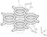
도 2에는 본 발명의 제1 실시예에 따른 플라즈마 디스플레이 패널이 도시되어 있고, 도 3에는 도 2의 Ⅲ-Ⅲ 선을 따라 취한 수직 단면도가 도시되어 있다. 도면들을 참조하면, 상기 플라즈마 디스플레이 패널은 서로 상하로 이격되어 있는 전면기판(110) 및 배면기판(120)과, 상기 기판들(110,120) 사이에서 복수 개의 방전셀(S)들을 구획하는 격벽(130)을 포함한다. 상기 전면기판(110)은 소정의 영상이 투영되는 영상 표시면으로 제공될 수 있으며, 이를 위해, 광투과도가 높은 유리 소재의 글라스 기판으로 마련될 수 있다. 상기 격벽(130)은 전면기판(110) 및 배면기판(120) 사이에서 다수의 방전셀(S)들을 각기 독립적인 발광영역으로 구획한다. 도면으로 예시된 실시예에서는 상기 격벽(130)에 의해 원형의 횡단면을 갖는 방전셀(S)들이 구획되는데, 이로써 방전셀(S) 내에는 그 셀 축을 중심으로 대칭적인 전계가 형성되며, 방전셀(S) 중앙으로 플라즈마를 집중시켜 하전입자와의 충돌에 의한 방전가스의 여기를 촉진할 수 있다. 다만, 상기 방전셀(S)의 형상은 이에 한정되지 않으며, 격벽(130)의 형상을 다양하게 변화시킴으로써, 사각형, 오각형, 육각형을 포함하는 다각형이나, 타원형 등의 다양한 비원형 횡단면의 방전셀들(S)이 구 획될 수 있다.2 illustrates a plasma display panel according to a first embodiment of the present invention, and FIG. 3 illustrates a vertical cross-sectional view taken along the line III-III of FIG. 2. Referring to the drawings, the plasma display panel partitions the
상기 격벽(130)은 충분한 내전압 특성을 갖도록 소정의 비유전율을 갖는 유전체로 이루어질 수 있으며, 방전시 제1 방전전극(131) 및 제2 방전전극(132)이 직접 통전되는 것을 방지하고, 벽전하의 축적을 유도하는 등 방전에 유리한 환경을 제공한다. 방전셀(S)과 직접 접하는 격벽(130)의 측벽에는 하전입자와의 충돌에 의한 격벽(130) 손상을 방지하기 위해, 별도의 보호층(135)이 덮여 있는 것이 바람직하며, 상기 보호층(135)은, 예를 들어, MgO 박막으로 구성될 수 있다.The
상기 격벽(130) 내에는 상하로 이격되어 있는 제1, 제2 방전전극(131,132)이 매립되어 있다. 도 4에는 도 2에 도시된 방전전극들(131,132)의 배치 구조가 도시되어 있다. 도면을 참조하면, 상기 제1 방전전극(131)들은 일 열로 배열된 방전셀(S)들을 둘러싸면서 x 방향으로 나란하게 연장된다. 각 방전전극(131)들은 인접한 방전전극(131)과 이격되게 배치되며, 외부전원과 접속된 단부를 통해 각기 다른 전기적 신호를 인가받는다. 상기 제1 방전전극(131)은 방전셀(S)을 둘러싸면서 직접 방전에 참여하는 방전부(131a) 및 인접한 방전부(131a)들을 상호 전기적으로 연결하는 통전부(131b)를 구비한다. 상기 방전부(131a)는 방전셀(S) 내부에 방전을 일으키기 위한 소정의 전계를 형성하며, 이러한 목적을 달성할 수 있는 한, 상기 방전부(131a)는 폐쇄된 루프 구조로 형성되어 방전셀(S) 외주를 전부 둘러싸는 것도 가능하지만, 이와 달리, 방전셀(S) 외주를 따라 일부가 개방된 형태로 마련되는 것도 가능하다. 상기 통전부(131b)는 인접한 방전부(131a)들 사이에서 일체로 형성되어, 각 방전전극(131)에 속한 방전부(131a)들이 서로 동일한 구동신호를 공유하 도록 한다. 다만, 통전부(131b) 없이 방전부(131a)들이 서로 연속적으로 이어지더라도 동일한 구동신호를 공유할 수 있으므로, 통전부(131b)가 방전전극(131)을 구성하기 위한 필수적인 사항은 아니다.In the
상기 제2 방전전극(132)은 상기 제1 방전전극(131)의 하방에 이격되게 배치된다. 상기 제2 방전전극(132)도 전술한 제1 방전전극(131)과 유사한 구성을 갖는다. 따라서, 방전셀(S)들을 둘러싸는 방전부(132a) 및 인접한 방전부(132a)들 사이를 전기적으로 이어주는 통전부(132b)를 구비한다. 상기 제2 방전전극(132)은 상기 제1 방전전극(131)과 다른 방향을 따라 연장되는데, 예를 들어, 제1 방전전극(131)과 직교하는 y 방향으로 연장될 수 있다. 이렇게 제1, 제2 방전전극(131,132)이 서로 교차되는 방향으로 연장되는 것은 디스플레이의 PM(Passive Matrix) 구동을 위한 것으로, 일 방전전극(131)은 어드레스 전극으로 기능하고, 다른 방전전극(132)은 주사전극으로 기능함으로써, 표시방전을 일으킬 방전셀(S)에 대한 선택동작이 가능하도록 하기 위한 것이다. 예를 들어, 상기 제1 방전전극(131)은 주사전극으로, 상기 제2 방전전극(132)은 어드레스 전극으로 구동될 수 있다.The
한편, 상기 방전전극들(131,132)은 자체 저항에 의한 전압강하를 막기 위해, 전기 전도도가 우수한 금속소재로 형성될 수 있으며, 예를 들어, Al, Cu, Ag 등으로 이루어질 수 있다. 상기 제1, 제2 방전전극들(131,132) 사이에 방전을 일으키기에 충분한 소정의 교류전압이 인가되면, 방전셀(S) 내부에는 인가된 전압에 따라 소정의 전계가 형성되면서 방전셀(S)들을 한정하는 격벽(130)의 측면을 통하여 수직 방향으로 방전이 개시된다.Meanwhile, the
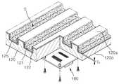
상기 배면기판(120)은 서로 마주보게 결합되는 전면기판(110)과 함께 내부에 수용된 방전가스의 유출을 막고, 격벽(130)과 함께 다수의 방전셀(S)들을 한정한다. 본 발명에서, 상기 배면기판(120)은 원소재가 되는 금속 플레이트의 일면에 다수의 제1 그루브(121) 패턴을 형성한 후, 아노다이징(Anodizing) 등의 산화처리를 거쳐서 그루브(121) 패턴이 형성된 제1 면(120a)에 소정 두께(To)로 산화피막(122)을 형성한 일체형 플레이트이다. 배면기판(120)에 형성된 제1 그루브(121)들은 일 열의 방전셀(S)들에 대응되도록 소정간격을 두고 스트라이프 패턴으로 형성될 수 있다. 상기 제1 그루브(121)는 형광체(125)가 도포되는 영역을 구획하기 위한 것으로, 수직 단차를 형성하는 그루브(121)들 사이 영역에 의해 인접한 서로 다른 발광색의 형광체(125)가 혼색되지 않도록 하고, 그루브(121)를 형성하는 바닥면 및 측면을 통해 도포면적을 증대하여 발광효율에 기여한다. 예를 들어, 서로 다른 발광색의 R,G,B 형광체(125)가 그루브(121)들에 도포됨에 따라, 대응되는 방전셀(S)들은 각각 적색, 녹색, 및 청색 광을 발하는 R,G,B 부화소로 형성되며, 인접한 R,G,B 부화소들이 모여서 하나의 단위 화소를 구성하게 된다.The
한편, 상기 전면기판(110)에도 형광체(125)가 도포되는 제2 그루브(111)가 형성될 수 있다. 상기 제2 그루브(111)는 일 열의 방전셀(S)들에 대응하여 소정간격을 두고 나란하게 연장되는 스트라이프 패턴으로 형성될 수 있다. 상기 제2 그루브(111)는 배면기판(120) 측의 제1 그루브(121) 이외에 추가적으로 형광체(125)에 대한 도포면을 제공함으로써, 디스플레이의 발광효율에 기여할 수 있다. 즉, 각 방전셀(S)에 대응되는 상부와 하부영역에 모두 형광체(125)가 도포됨으로써, 방전결 과로 생성된 자외선이 투명한 전면기판(110)을 투과하여 무효하게 외부로 손실되는 것을 방지하고, 발광에 기여하는 가시광으로 변환되도록 함으로써, 디스플레이 패널의 발광효율을 높일 수 있는 것이다. 혼색방지를 위해, 상기 전면기판(110) 측과 배면기판(120) 측의 형광체(125)는 상하로 대응되는 위치에 동일한 발광색으로 도포되어야 할 것이다.Meanwhile, a
한편, 본 발명의 배면기판(120)은 종래 글라스 기판과 샤시베이스의 기능을 함께 수행할 수 있는 샤시베이스-일체형으로 마련되므로, 종래 샤시베이스의 역할도 담당하게 된다. 이하에서는 도 5를 참조하여 이에 대해 상세히 설명하기로 한다.On the other hand, since the
상기 배면기판(120)에는 플라즈마 디스플레이 장치에 구비되는 다른 구성부품들이 직간접적으로 지지되는데, 제1 면(120a)을 통해 전면기판(110) 및 격벽(130)을 지지함으로써 외부충격으로부터 구성부품이 파손되지 않도록 보호하며, 또한, 제2 면(120b)을 통해 회로구동부(160)를 지지함으로써 회로구동부(160)에 대한 설치면을 제공할 수 있다. 상기 회로구동부(160)는 소정의 구동신호를 발생하고, 이를 방전전극(131,132)에 인가하기 위한 다수의 구동IC 및 회로기판들을 포함하여 이루어질 수 있다.The
상기 배면기판(120)은 지지구조로서 충분한 강성을 제공할 수 있으면서도, 후술하는 바와 같이 방열 및 접지목적을 위해, 우수한 열 및 전기전도 특성을 겸비한 알루미늄 플레이트로 이루어질 수 있다. 상기 배면기판(120)은 방전 횟수에 따라 일부 방전셀(S)들에서 집중적으로 발생되는 열을 그 자신을 통해 평면방향으로 신속히 전파하여 국부적으로 일부 영역에 열이 축적되지 않도록 한다. 이와 함께, 외부로 노출된 제2 면(120b)을 통하여 방전으로 발생된 열을 저온의 대기중으로 방출시키는 방열기능을 수행한다. 방전으로 인한 발열뿐 아니라, 배면기판(120)의 제2 면(120b)에 설치된 회로구동부(160)도 다수의 발열소자들을 포함하고 있는바, 상기 배면기판(120)은 이들 발열소자에 대한 방열판 역할을 겸하게 된다.The
또한, 전기 전도성이 우수한 금속소재로 이루어지는 배면기판(120)은 넓은 면적에 걸쳐 균일한 그라운드 전압을 유지하는 접지 영역을 형성할 수 있다. 이에, 구동회로부(160)를 구성하는 다수의 구동IC나 회로기판 등은 상기 배면기판(120)에 직접 접지됨으로써 공통의 그라운드 전압을 유지할 수 있다.In addition, the
한편, 그루부(121)가 형성된 배면기판(120)의 제1 면(120a)을 따라 산화피막(122)이 형성되어 있는데, 그루브(121) 영역 및 그루브(121)들 사이 영역에 걸쳐서 대략 균일한 두께 To로 형성되어 있다. 상기 산화피막(122)은 원소재인 알루미늄 플레이트에 대한 산화물인 알루미나(Al2O3)로 이루어진다. 상기 산화피막(122)의 두께(To)는 표면으로부터 내부로 산화가 진행되는 아노다이징(Anodizing)의 공정조건, 예를 들어, 공정시간, 인가전류의 세기, 전해용액의 선택 등을 적절히 조절함으로써 최적화시킬 수 있으며, 요구되는 내전압 특성을 고려하여 1μm - 50 μm의 범위에서 선택될 수 있다. 이렇게 수 내지 수십 μm의 박막으로 형성된 산화피막(122)은 치밀한 내부조직을 바탕으로 충분한 내전압 특성을 제공할 수 있는데, 예를 들어, 20μm 두께의 산화피막은 대략 500V 의 전압에도 절연파괴 없이 견딜 수 있다. 산화피막(122)이 형성된 배면기판(120)은 방전셀(S)들을 한정하는 전면기 판(110) 및 격벽(130)과 함께, 절연된 방전환경을 제공하며, 여기서, 상기 산화피막(122)은 전기 전도성이 우수한 알루미늄 소재가 방전셀(S)에 직접 노출되어 방전환경에 영향을 주지 못하도록 방전셀(S)과의 사이에 절연 경계층을 형성한다.Meanwhile, an
이와 같이, 방전셀(S)과 직접 접하는 배면기판(120)의 제1 면(120a)에는 인위적인 산화공정을 거쳐 충분한 두께(To)의 산화피막(122)을 형성할 필요가 있다. 그러나, 외부대기와 접하게 되는 배면기판(120)의 제2 면(120b)은 적어도 전기적으로 절연화될 필요는 없으며, 오히려, 방열이나 접지목적을 위해 알루미늄 고유의 높은 전도 특성을 갖는 것이 유리할 수 있다. 다만, 자연 상태에서도 높은 알루미늄-산소의 친화력 및 알루미늄 소재의 표면에 치밀한 산화막을 형성하는 것이 내구성 측면에서 유리할 수 있다는 점 등을 고려하여, 배면기판(120)의 제2 면(120b)에도 인위적인 아노다이징 공정이나, 자연 상태의 방치를 통해 추가적인 산화피막(미도시)이 형성될 수 있다. 이 경우, 배면기판(120)의 제1 면(120a)과 제2 면(120b)에 각각 형성되는 산화피막은 그 목적이 상이한 만큼 두께가 서로 다를 수 있다.As such, it is necessary to form an
일반적으로, 아노다이징 등의 산화공정에서는 전해용액이 수용된 욕조 속에서 가공물의 노출된 모든 표면을 통해 산화가 진행되므로, 선택적으로 배면기판(120)의 제1 면(120a)에 대해서만 산화처리하고, 제2 면(120b)에 대해서는 산화를 막고자 한다면, 산화공정시 제2 면(120b)을 소정의 산화방지용 마스크(미도시)으로 덮어 산소가 침투되지 않도록 한다. 대안으로, 배면기판(120)의 제1, 제2 면(120a,120b)에서 진행되는 산화 속도를 조절하기 위해, 제2 면(120b)을 산화지연막으로 덮어 양쪽 면에서 형성되는 산화피막의 두께를 서로 다르게 조절할 수도 있다.In general, in the oxidation process such as anodizing, oxidation proceeds through all exposed surfaces of the workpiece in the bath containing the electrolytic solution, and thus selectively oxidizes only the
종래에는 소재 자체로 절연성을 갖는 글라스 기판을 통하여, 절연된 방전환경을 제공하고, 글라스 기판과 별도로 알루미늄 소재로 된 샤시베이스를 설치함으로써, 디스플레이 패널과 회로구동부에 대한 구조적인 지지 및 방열을 담당하도록 하고 있다. 본 발명에서 배면기판 자체는 전기 및 열 전도성이 우수한 알루미늄 등의 금속소재로 형성하되, 그 표면에 높은 내전압 특성을 갖는 산화피막(122)을 형성함으로써, 종래 별도의 목적을 위해 각기 준비되던 글라스 기판 및 샤시베이스의 역할을 하나의 샤시베이스 일체형 배면기판이 담당하도록 하고 있다. 이는 구성부품의 개수 및 조립공수의 감축을 통해 디스플레이 장치의 원가 절감이 가능함은 물론, 박형화 및 경량화에 유리한 디스플레이 장치가 제공될 수 있음을 의미하는 것이다.Conventionally, the insulating material itself is used to provide an insulated discharge environment, and by installing a chassis base made of an aluminum material separately from the glass substrate, so as to perform structural support and heat dissipation for the display panel and the circuit driver. Doing. In the present invention, the back substrate itself is formed of a metal material such as aluminum having excellent electrical and thermal conductivity, and by forming an
이하에서는 도 5에 도시된 배면기판(120)의 제조방법에 대해 도 6a 내지 도 6i를 참조하여, 공정단계별로 설명하기로 한다. 먼저, 도 6a에서 볼 수 있듯이, 배면기판의 원소재가 되는 금속 플레이트를 준비하는데, 예를 들어, 우수한 전도성 및 산소와의 친화력이 높아 산화도가 우수한 알루미늄 플레이트(120`)로 마련될 수 있다. 다음으로, 도 6b에 도시된 바와 같이, 제공된 알루미늄 시트(120`)의 일면에 포토리지스트(P)를 도포한다. 상기 포토리지스트(P)는 UV 등의 조사광에 노출되면 화학적인 반응을 통해 경화되는 감광성 수지재로 이루어질 수 있다.Hereinafter, a method of manufacturing the
다음으로, 노광 마스크(M)를 통해 포토리지스트(P)에 대해 선택적으로 UV 광 을 조사하는 노광과정 및 이어지는 현상과정을 통해, 도 6c에 도시된 바와 같이, 소정의 패턴이 형성된 PR 마스크(PR)를 형성한다. 상기 PR 마스크(PR)는 그루브 부분(W1)에 대응되는 개구 패턴을 갖고, 해당 부분을 노출시킨다. 이때, 상기 그루브 부분(W1)은 방전셀(S)에 대응되는 위치에 설계된다.Next, through the exposure process of selectively irradiating UV light to the photoresist P through the exposure mask M and the subsequent developing process, as shown in FIG. PR). The PR mask PR has an opening pattern corresponding to the groove portion W1 and exposes the portion. In this case, the groove portion W1 is designed at a position corresponding to the discharge cell S.
다음에는 도 6d 및 도 6e에서 볼 수 있듯이, PR 마스크(PR)를 식각 방지막으로 하여, 알루미늄 플레이트(120`)에 대해 에칭을 실시한다. 이를 통해, 그루브 부분(W1)이 선택적으로 식각되면서 그루브(121)가 형성되고, 그루브 사이 부분(W2)과 수직 단차를 형성하게 된다.Next, as shown in FIGS. 6D and 6E, the
다음으로, 알루미늄 플레이트(120`)의 제1 면(120`a) 및 제2 면(120`b) 중에서, 후술하는 산화공정을 통해 절연층이 형성될 면을 선택하는데, 적어도 방전셀(S)과 맞닿게 되는 제1 면(120`a)에는 절연층으로서 산화피막(122)이 형성되는 것이 바람직하다. 예를 들어, 알루미늄 플레이트(120`)의 제1 면(120`a)만을 선택적으로 산화시키고자 한다면, 제2 면(120`b)에는 도 6f에 도시된 바와 같이, 산소의 접근을 차단하기 위한 산화방지용 마스크(OB)를 형성한다.Next, from among the first surface 120'a and the second surface 120'b of the
다음으로, 도 6g에 도시된 바와 같이, 상기 알루미늄 플레이트(120`)에 대해 공지의 산화처리를 통하여 그 표면에 산화피막(122)을 형성하는 아노다이징 공정이 진행된다. 상기 아노다이징 공정에서는, 예를 들어, H2SO4 등의 산성 전해용액 속에서 상기 알루미늄 시트를 양극(+)으로, 촉매로 작용하는 Pt,Ni,Carbon 소재를 음극(-)으로 하여 직류전원을 통전하면, 전기화학적인 반응을 통해 알루미늄 표면으로부터 내부로 산화가 진행되면서 산화피막(122)이 형성된다. 이때, 산화피막(122)의 두께(To)는 아노다이징의 구체적인 공정조건, 예를 들어, 전해용액의 종류나 공정시간, 직류전압의 세기 등을 조정하여 최적으로 제어될 수 있으며, 예를 들어, 1μm ~ 50μm 범위로 조절될 수 있다. 알루미늄 플레이트(120`)의 제1 면(120`a)을 따라 생성되는 산화피막(122)은 알루미나(Al2O3)로 이루어지고, 절연성을 갖는 세라믹 소재가 된다. 이때, 상기 산화방지용 마스크(OB)는 제2 면(120`b)을 통해 알루미늄 플레이트(120`) 내부로 산소가 침투되지 않도록 산소의 접근을 차단함으로써 산화피막의 형성을 막는다.Next, as shown in FIG. 6G, an anodizing process of forming an
다음으로, 산화방지용 마스크(OB)를 박리하면 도 6h에 도시된 바와 같이 완성된 형태의 배면기판(120)을 얻을 수 있다. 다음으로, 도 6i에 도시된 바와 같이, 상기 그루브(121)에 의해 구획된 영역에 R,G,B 형광체(125)를 도포한다. 일 방향으로 연장된 각 그루브(121)에 대해 선택된 발광색의 형광체(125)를 도포하는데, 예를 들어, 일정한 개구 패턴이 형성된 스크린(미도시)을 통해 형광체 페이스트를 소정 영역에 도포하는 스크린 인쇄법이나 형광체 페이스트를 토출하면서 일정한 속도로 주행하는 분사 노즐을 구비하는 디스펜서를 이용하는 디스펜싱 방법 등이 이용될 수 있다.Next, by peeling the anti-oxidation mask (OB) it can be obtained a
전술한 공정들을 통해 얻어진 배면기판(120)을 이용하고, 도 6j를 참조하여 설명될 이하의 공정을 통하여, 플라즈마 디스플레이 장치가 제공될 수 있다. 먼저, 제1 내지 제5 격벽용 시트들(130a,130b,130c,130d,130e)을 순차적으로 적층하여 방전전극(131,132)이 매립되어 있는 격벽(130)을 형성하게 된다. 여기서, 선택된 일부 격벽용 시트들(130b,130d)에는 전극패턴이 형성되어 있는데, 예를 들어, 제2 격 벽용 시트(130b)에는 제1 방전전극(131)이 패턴화되어 있고, 제4 격벽용 시트(130d)에는 제2 방전전극(132)이 패턴화되어 있다. 그리고, 나머지 다른 격벽용 시트들, 즉, 제1, 제3, 제5 격벽용 시트(130a,130c,130e)는 사실상 동일한 유전체 시트로 이루어질 수 있다.Using the
이렇게 격벽용 시트들(130a,130b,130c,130d,130e)을 적층한 후, 고온의 소성 공정을 통해 이들(130a,130b,130c,130d,130e)이 서로 융착되어 일체화되도록 한다. 다음으로, 일체화된 격벽용 시트들(130a,130b,130c,130d,130e)에 대해 일정한 개구 패턴을 형성하도록 펀칭가공을 실사함으로써 방전셀(S)을 형성한다. 그리고, 상기 방전셀(S)의 측면에 스퍼터링에 의해 보호막(135)으로 기능하는 MgO 박막을 형성한다. 한편, 본 설명에서는 5개의 격벽용 시트(130a,130b,130c,130d,130e)를 적층하는 것에 의해 충분한 높이의 격벽(130)이 구성되는 것으로 가정하였으나, 이는 이해의 편의를 위한 것일 뿐이며, 실제 적용에 있어서는 충분한 방전셀(S) 공간을 확보하기 위해 다수의 격벽용 시트가 마련될 수 있음은 물론이다.After stacking the
한편, 전면기판(110)은 글라스 기판의 소정위치에 그루브(111)를 형성한 후, 그루브(111) 내에 R,G,B 형광체(125)를 도포함으로써 제공될 수 있다. 마지막으로, 준비된 격벽(130)을 사이에 두고 상기 전면기판(110)과 배면기판(120)을 수직으로 정렬시킨 후, 테두리를 따라 도포된 프릿 실링제(180)를 통하여 서로 대면되게 결합하는 것에 의하여, 플라즈마 디스플레이 장치의 주요부가 완성된다. 이후, 상기 배면기판(120)에는 방전전극(131,132)에 인가되는 구동신호를 발생하고 전달하기 위한 다수의 구동IC 및 회로기판들을 포함하는 회로구동부가 설치될 수 있다.Meanwhile, the
(제2 실시예)(2nd Example)
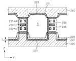
도 7에는 본 발명의 제2 실시예에 따른 플라즈마 디스플레이 장치의 분해 사시도가 도시되어 있으며, 도 8 및 도 9에는 각각 도 7의 Ⅷ-Ⅷ 선을 따라 취한 수직 단면도 및 도 7에 도시된 방전전극들의 배치구조가 도시되어 있다. 본 실시예의 플라즈마 디스플레이 장치도 전술한 바와 유사하게, 서로 마주보게 배치된 전면기판(210) 및 배면기판(220)을 갖고, 상기 기판들(210,220) 사이에는 복수의 방전셀(S)들을 구획하는 격벽(230)이 배치된다. 상기 배면기판(220)은 그루브(221) 패턴이 나란하게 형성된 알루미늄 플레이트를 아노다이징 등의 산화처리를 함으로써, 적어도 그 일 표면(220a)에 산화피막(222)을 형성한 기판이다. 이에 따라, 상기 배면기판(220)은 샤시베이스 일체형으로 마련되며, 일면(220a) 및 타면(220b)을 통해 전면기판(210), 격벽(230) 및 회로구동부(미도시) 등을 지지하는 역할과, 지지된 구조들에 대한 방열판 역할을 한다.FIG. 7 is an exploded perspective view of the plasma display device according to the second embodiment of the present invention. FIG. 8 and FIG. 9 are vertical sectional views taken along the line VII-VII of FIG. 7 and the discharge electrode shown in FIG. The arrangement of these is shown. Similar to the above, the plasma display device of the present embodiment has a
본 실시예에서는 3개의 방전전극(231,232,233)이 구비된다는 점에서 전술한 실시예와 구조상 차별된다. 상기 방전전극들(231,232,233)의 배치구조에 관한 도 9를 참조하면, 제1 내지 제3 방전전극들(231,232,233)은 열을 지어 배열된 방전셀(S)들을 둘러싸면서 연장된다. 이때, 상기 제1 내지 제3 방전전극들(231,232,233)은 방전셀(S)들을 서로 다른 수직 높이에서 둘러싸면서 각 방향으로 연장되며, 방전셀(S)을 둘러싸는 방전부(231a,232a,233a) 및 인접한 방전부(231a,232a,233a)들을 상호 전기적으로 연결하는 통전부(231b,232b,233b)를 포함하여 구성된다. 여기서, 상기 제1, 제2 방전전극(231,232)은 방전셀(S)에 대해 함 께 표시방전을 일으키기 위한 것으로, 상하로 나란하게 x 방향을 따라 연장되며, 이들(231,232) 사이에 방전을 일으킬 수 있는 소정의 교류펄스를 인가함으로써, 방전셀(S)들에 표시방전을 일으키게 된다.In the present embodiment, three
상기 제3 방전전극(233)은 상기 제1, 제2 방전전극들(231,232) 사이에서 이들과 교차하는 방향, 예를 들어, 직교하는 y 방향으로 연장된다. 상기 제3 방전전극(232)은 상기 제1 방전전극(231) 또는 제2 방전전극(232)과 함께 방전셀(S)의 선택을 위한 어드레스 방전을 일으키기 위한 것이다. 여기서, 상기 어드레스 방전은 표시방전이 원활히 일어날 수 있도록 도와주는 일종의 예비적인 보조방전을 의미한다. 한편, 본 실시예에 있어서도 발광효율을 고려하여 전면기판(210) 측에도 형광체(225)를 도포하기 위한 추가적인 그루브(211)가 형성될 수 있음은 물론이다. 그리고, 상기 방전셀(S)을 구획하는 격벽(230)의 측면에는 보호막(235)이 형성되어 있는 것이 바람직하다.The
본 발명에서는 배면기판 자체는 알루미늄 등의 전도성이 우수한 금속소재로 형성하되, 절연된 방전환경을 제공하기 위해 상기 배면기판 표면에 내전압 특성이 우수한 산화피막을 형성함으로써, 종래 각기 마련되던 글라스 기판과 샤시베이스의 기능을 단일 부품으로 된 샤시베이스 일체형 배면기판이 담당하도록 하며, 이로써, 구성부품 개수가 감축되는 효과가 있다. 특히, 글라스 기판 및 샤시베이스를 대면 결합하기 위한 양면 테이프 및 열전달 목적의 방열시트 등이 제거됨으로써, 구성부품의 감축이 배가될 수 있다. 또한, 종래 글라스 기판과 샤시베이스를 서로 결합하 기 위한 가압 결합공정이 제거될 수 있으므로, 조립공정 또한 감축되는 효과가 있다.In the present invention, the back substrate itself is formed of a metal material having excellent conductivity such as aluminum, but by forming an oxide film having excellent withstand voltage characteristics on the surface of the back substrate to provide an insulated discharge environment, the glass substrate and the chassis, which are conventionally provided The function of the base is to be in charge of the chassis base integrated back substrate made of a single component, thereby reducing the number of components. In particular, since the double-sided tape and the heat dissipation sheet for heat transfer purposes are removed to face the glass substrate and the chassis base, the reduction of the component can be doubled. In addition, since the pressure bonding process for bonding the glass substrate and the chassis base to each other can be eliminated, the assembly process is also reduced.
또한, 방전셀에서 발생되는 고열이 외부대기로 방출되는 방열 경로 상에서, 열전도 특성이 떨어지는 글라스 기판이 제거됨에 의해, 방열 성능의 향상이라는 부수적인 목적도 달성할 수 있다.In addition, the secondary object of improving the heat dissipation performance can be achieved by removing the glass substrate having poor thermal conductivity from the heat dissipation path in which the high heat generated in the discharge cell is discharged to the outside atmosphere.
본 발명은 도면에 도시된 실시예를 참고로 설명되었으나 이는 예시적인 것에 불과하며, 본 기술 분야의 통상의 지식을 가진 자라면 이로부터 다양한 변형 및 균등한 다른 실시예가 가능하다는 점을 이해할 것이다. 따라서, 본 발명의 진정한 기술적 보호 범위는 첨부된 특허청구범위의 기술적 사상에 의하여 정해져야 할 것이다.Although the present invention has been described with reference to the embodiments shown in the drawings, this is merely exemplary, and it will be understood by those skilled in the art that various modifications and equivalent other embodiments are possible. Therefore, the true technical protection scope of the present invention will be defined by the technical spirit of the appended claims.
Claims (16)
Translated fromKoreanPriority Applications (4)
| Application Number | Priority Date | Filing Date | Title |
|---|---|---|---|
| KR1020060106997AKR100829746B1 (en) | 2006-11-01 | 2006-11-01 | Plasma display device and manufacturing method thereof |
| US11/860,448US7652428B2 (en) | 2006-11-01 | 2007-09-24 | Plasma display apparatus and manufacturing method of the same |
| EP07118449AEP1918961B1 (en) | 2006-11-01 | 2007-10-15 | Plasma display apparatus and manufacturing method of the same |
| DE602007005899TDE602007005899D1 (en) | 2006-11-01 | 2007-10-15 | Plasma display device and method for its production |
Applications Claiming Priority (1)
| Application Number | Priority Date | Filing Date | Title |
|---|---|---|---|
| KR1020060106997AKR100829746B1 (en) | 2006-11-01 | 2006-11-01 | Plasma display device and manufacturing method thereof |
Publications (2)
| Publication Number | Publication Date |
|---|---|
| KR20080039564A KR20080039564A (en) | 2008-05-07 |
| KR100829746B1true KR100829746B1 (en) | 2008-05-19 |
Family
ID=38972997
Family Applications (1)
| Application Number | Title | Priority Date | Filing Date |
|---|---|---|---|
| KR1020060106997AExpired - Fee RelatedKR100829746B1 (en) | 2006-11-01 | 2006-11-01 | Plasma display device and manufacturing method thereof |
Country Status (4)
| Country | Link |
|---|---|
| US (1) | US7652428B2 (en) |
| EP (1) | EP1918961B1 (en) |
| KR (1) | KR100829746B1 (en) |
| DE (1) | DE602007005899D1 (en) |
Families Citing this family (4)
| Publication number | Priority date | Publication date | Assignee | Title |
|---|---|---|---|---|
| KR100838083B1 (en)* | 2007-03-21 | 2008-06-16 | 삼성에스디아이 주식회사 | Manufacturing method of plasma display panel and plasma display panel |
| KR100836428B1 (en)* | 2007-04-06 | 2008-06-09 | 삼성에스디아이 주식회사 | Electrode sheet for plasma display panel and plasma display panel using same |
| WO2015000095A1 (en) | 2013-07-05 | 2015-01-08 | Industrial Technology Research Institute | Flexible display and method for fabricating the same |
| KR101828646B1 (en)* | 2014-08-11 | 2018-02-13 | 주식회사 엘지화학 | Aluminium pattern and method for forming aluminium pattern |
Citations (5)
| Publication number | Priority date | Publication date | Assignee | Title |
|---|---|---|---|---|
| JPH0815677A (en)* | 1994-06-29 | 1996-01-19 | Sony Corp | Plasma address display device |
| KR19990042897A (en)* | 1997-11-28 | 1999-06-15 | 구자홍 | High Pressure Discharge Type Color Plasma Display Panel |
| KR20030039463A (en)* | 2001-11-13 | 2003-05-22 | 오리온전기 주식회사 | method of making a plasma display panel |
| JP2004162087A (en) | 2002-11-11 | 2004-06-10 | Hitachi Metals Ltd | Metal partition for plasma display |
| KR20040080373A (en)* | 2003-03-11 | 2004-09-18 | 엘지전자 주식회사 | Plasma Display Panel and Method of Fabricating The Same |
Family Cites Families (9)
| Publication number | Priority date | Publication date | Assignee | Title |
|---|---|---|---|---|
| US5053673A (en)* | 1988-10-17 | 1991-10-01 | Matsushita Electric Industrial Co., Ltd. | Field emission cathodes and method of manufacture thereof |
| JPH06168669A (en) | 1992-04-21 | 1994-06-14 | T T T:Kk | Discharge display device formed by using thin plate metal board |
| KR19980065367A (en)* | 1996-06-02 | 1998-10-15 | 오평희 | Backlight for LCD |
| JPH10116556A (en) | 1996-10-14 | 1998-05-06 | Matsushita Electric Ind Co Ltd | Partition structure of plasma display and method of forming the same |
| KR100295112B1 (en)* | 1998-12-02 | 2001-07-12 | 구자홍 | Lower substrate for plasma display device |
| KR20040087905A (en) | 2003-04-09 | 2004-10-15 | 파이오니아 가부시키가이샤 | Plasma display panel |
| KR100551902B1 (en) | 2004-02-05 | 2006-02-16 | 한국기계연구원 | Rear plate of Plasma Display Panel |
| KR100603414B1 (en)* | 2005-01-26 | 2006-07-20 | 삼성에스디아이 주식회사 | Plasma display panel and flat panel display device having same |
| KR100637245B1 (en)* | 2005-08-29 | 2006-10-23 | 삼성에스디아이 주식회사 | DC plasma display panel and manufacturing method thereof |
- 2006
- 2006-11-01KRKR1020060106997Apatent/KR100829746B1/ennot_activeExpired - Fee Related
- 2007
- 2007-09-24USUS11/860,448patent/US7652428B2/ennot_activeExpired - Fee Related
- 2007-10-15DEDE602007005899Tpatent/DE602007005899D1/enactiveActive
- 2007-10-15EPEP07118449Apatent/EP1918961B1/ennot_activeNot-in-force
Patent Citations (5)
| Publication number | Priority date | Publication date | Assignee | Title |
|---|---|---|---|---|
| JPH0815677A (en)* | 1994-06-29 | 1996-01-19 | Sony Corp | Plasma address display device |
| KR19990042897A (en)* | 1997-11-28 | 1999-06-15 | 구자홍 | High Pressure Discharge Type Color Plasma Display Panel |
| KR20030039463A (en)* | 2001-11-13 | 2003-05-22 | 오리온전기 주식회사 | method of making a plasma display panel |
| JP2004162087A (en) | 2002-11-11 | 2004-06-10 | Hitachi Metals Ltd | Metal partition for plasma display |
| KR20040080373A (en)* | 2003-03-11 | 2004-09-18 | 엘지전자 주식회사 | Plasma Display Panel and Method of Fabricating The Same |
Also Published As
| Publication number | Publication date |
|---|---|
| US20080100217A1 (en) | 2008-05-01 |
| US7652428B2 (en) | 2010-01-26 |
| DE602007005899D1 (en) | 2010-05-27 |
| KR20080039564A (en) | 2008-05-07 |
| EP1918961B1 (en) | 2010-04-14 |
| EP1918961A1 (en) | 2008-05-07 |
Similar Documents
| Publication | Publication Date | Title |
|---|---|---|
| KR100254003B1 (en) | Gas discharge display panel and manufacturing method thereof | |
| KR20040036635A (en) | Planar display device and sealing method thereof | |
| KR100829746B1 (en) | Plasma display device and manufacturing method thereof | |
| JP4436918B2 (en) | Plasma display panel | |
| JP2001084913A (en) | Gas discharge type display panel | |
| US7583025B2 (en) | Plasma display module and method of manufacturing the same | |
| US20080084154A1 (en) | Plasma display panel and method of manufacturing the same | |
| US20080036381A1 (en) | Plasma display panel and method of fabricating the same | |
| JP2001052622A (en) | Flat plasma discharge display device | |
| KR100869109B1 (en) | Plasma display panel having alignment mark portion, and manufacturing method thereof | |
| US6864632B2 (en) | Front plate structure for plasma display panel | |
| KR20080039565A (en) | Plasma display panel | |
| JP4085223B2 (en) | Plasma display device | |
| US20070152595A1 (en) | Plasma display panel | |
| JPH10116556A (en) | Partition structure of plasma display and method of forming the same | |
| JPH09251842A (en) | Gas discharge display panel and manufacturing method thereof | |
| JP2000243303A (en) | Structure for back side substrate of discharge type display device | |
| US7489080B2 (en) | Direct current plasma panel (DC-PDP) and method of manufacturing the same | |
| JP5264419B2 (en) | Image display device | |
| JPWO2011010385A1 (en) | Luminescent screen and image display device | |
| KR100759448B1 (en) | Plasma display device and manufacturing method thereof | |
| US20080018249A1 (en) | Plasma display panel and production process of same | |
| US20060214558A1 (en) | Image display device | |
| KR100751375B1 (en) | Plasma display panel and flat panel display device having same | |
| KR100528921B1 (en) | Plasma display panel |
Legal Events
| Date | Code | Title | Description |
|---|---|---|---|
| A201 | Request for examination | ||
| PA0109 | Patent application | St.27 status event code:A-0-1-A10-A12-nap-PA0109 | |
| PA0201 | Request for examination | St.27 status event code:A-1-2-D10-D11-exm-PA0201 | |
| D13-X000 | Search requested | St.27 status event code:A-1-2-D10-D13-srh-X000 | |
| D14-X000 | Search report completed | St.27 status event code:A-1-2-D10-D14-srh-X000 | |
| E902 | Notification of reason for refusal | ||
| PE0902 | Notice of grounds for rejection | St.27 status event code:A-1-2-D10-D21-exm-PE0902 | |
| P11-X000 | Amendment of application requested | St.27 status event code:A-2-2-P10-P11-nap-X000 | |
| P13-X000 | Application amended | St.27 status event code:A-2-2-P10-P13-nap-X000 | |
| E701 | Decision to grant or registration of patent right | ||
| PE0701 | Decision of registration | St.27 status event code:A-1-2-D10-D22-exm-PE0701 | |
| PG1501 | Laying open of application | St.27 status event code:A-1-1-Q10-Q12-nap-PG1501 | |
| GRNT | Written decision to grant | ||
| PR0701 | Registration of establishment | St.27 status event code:A-2-4-F10-F11-exm-PR0701 | |
| PR1002 | Payment of registration fee | St.27 status event code:A-2-2-U10-U11-oth-PR1002 Fee payment year number:1 | |
| PG1601 | Publication of registration | St.27 status event code:A-4-4-Q10-Q13-nap-PG1601 | |
| R18-X000 | Changes to party contact information recorded | St.27 status event code:A-5-5-R10-R18-oth-X000 | |
| R18-X000 | Changes to party contact information recorded | St.27 status event code:A-5-5-R10-R18-oth-X000 | |
| LAPS | Lapse due to unpaid annual fee | ||
| PC1903 | Unpaid annual fee | St.27 status event code:A-4-4-U10-U13-oth-PC1903 Not in force date:20110509 Payment event data comment text:Termination Category : DEFAULT_OF_REGISTRATION_FEE | |
| PC1903 | Unpaid annual fee | St.27 status event code:N-4-6-H10-H13-oth-PC1903 Ip right cessation event data comment text:Termination Category : DEFAULT_OF_REGISTRATION_FEE Not in force date:20110509 | |
| P22-X000 | Classification modified | St.27 status event code:A-4-4-P10-P22-nap-X000 | |
| R18-X000 | Changes to party contact information recorded | St.27 status event code:A-5-5-R10-R18-oth-X000 | |
| R18-X000 | Changes to party contact information recorded | St.27 status event code:A-5-5-R10-R18-oth-X000 |