KR100829323B1 - Plasma display apparatus - Google Patents
Plasma display apparatusDownload PDFInfo
- Publication number
- KR100829323B1 KR100829323B1KR1020010074142AKR20010074142AKR100829323B1KR 100829323 B1KR100829323 B1KR 100829323B1KR 1020010074142 AKR1020010074142 AKR 1020010074142AKR 20010074142 AKR20010074142 AKR 20010074142AKR 100829323 B1KR100829323 B1KR 100829323B1
- Authority
- KR
- South Korea
- Prior art keywords
- wiring
- electrodes
- electrode
- voltage
- driving circuit
- Prior art date
- Legal status (The legal status is an assumption and is not a legal conclusion. Google has not performed a legal analysis and makes no representation as to the accuracy of the status listed.)
- Expired - Fee Related
Links
Images


Classifications
- G—PHYSICS
- G09—EDUCATION; CRYPTOGRAPHY; DISPLAY; ADVERTISING; SEALS
- G09G—ARRANGEMENTS OR CIRCUITS FOR CONTROL OF INDICATING DEVICES USING STATIC MEANS TO PRESENT VARIABLE INFORMATION
- G09G3/00—Control arrangements or circuits, of interest only in connection with visual indicators other than cathode-ray tubes
- G09G3/20—Control arrangements or circuits, of interest only in connection with visual indicators other than cathode-ray tubes for presentation of an assembly of a number of characters, e.g. a page, by composing the assembly by combination of individual elements arranged in a matrix no fixed position being assigned to or needed to be assigned to the individual characters or partial characters
- G09G3/22—Control arrangements or circuits, of interest only in connection with visual indicators other than cathode-ray tubes for presentation of an assembly of a number of characters, e.g. a page, by composing the assembly by combination of individual elements arranged in a matrix no fixed position being assigned to or needed to be assigned to the individual characters or partial characters using controlled light sources
- G09G3/28—Control arrangements or circuits, of interest only in connection with visual indicators other than cathode-ray tubes for presentation of an assembly of a number of characters, e.g. a page, by composing the assembly by combination of individual elements arranged in a matrix no fixed position being assigned to or needed to be assigned to the individual characters or partial characters using controlled light sources using luminous gas-discharge panels, e.g. plasma panels
- G09G3/288—Control arrangements or circuits, of interest only in connection with visual indicators other than cathode-ray tubes for presentation of an assembly of a number of characters, e.g. a page, by composing the assembly by combination of individual elements arranged in a matrix no fixed position being assigned to or needed to be assigned to the individual characters or partial characters using controlled light sources using luminous gas-discharge panels, e.g. plasma panels using AC panels
- G09G3/296—Driving circuits for producing the waveforms applied to the driving electrodes
- G—PHYSICS
- G09—EDUCATION; CRYPTOGRAPHY; DISPLAY; ADVERTISING; SEALS
- G09G—ARRANGEMENTS OR CIRCUITS FOR CONTROL OF INDICATING DEVICES USING STATIC MEANS TO PRESENT VARIABLE INFORMATION
- G09G2320/00—Control of display operating conditions
- G09G2320/02—Improving the quality of display appearance
- G09G2320/0247—Flicker reduction other than flicker reduction circuits used for single beam cathode-ray tubes
- G—PHYSICS
- G09—EDUCATION; CRYPTOGRAPHY; DISPLAY; ADVERTISING; SEALS
- G09G—ARRANGEMENTS OR CIRCUITS FOR CONTROL OF INDICATING DEVICES USING STATIC MEANS TO PRESENT VARIABLE INFORMATION
- G09G2330/00—Aspects of power supply; Aspects of display protection and defect management
- G09G2330/06—Handling electromagnetic interferences [EMI], covering emitted as well as received electromagnetic radiation
- G—PHYSICS
- G09—EDUCATION; CRYPTOGRAPHY; DISPLAY; ADVERTISING; SEALS
- G09G—ARRANGEMENTS OR CIRCUITS FOR CONTROL OF INDICATING DEVICES USING STATIC MEANS TO PRESENT VARIABLE INFORMATION
- G09G3/00—Control arrangements or circuits, of interest only in connection with visual indicators other than cathode-ray tubes
- G09G3/20—Control arrangements or circuits, of interest only in connection with visual indicators other than cathode-ray tubes for presentation of an assembly of a number of characters, e.g. a page, by composing the assembly by combination of individual elements arranged in a matrix no fixed position being assigned to or needed to be assigned to the individual characters or partial characters
- G09G3/22—Control arrangements or circuits, of interest only in connection with visual indicators other than cathode-ray tubes for presentation of an assembly of a number of characters, e.g. a page, by composing the assembly by combination of individual elements arranged in a matrix no fixed position being assigned to or needed to be assigned to the individual characters or partial characters using controlled light sources
- G09G3/28—Control arrangements or circuits, of interest only in connection with visual indicators other than cathode-ray tubes for presentation of an assembly of a number of characters, e.g. a page, by composing the assembly by combination of individual elements arranged in a matrix no fixed position being assigned to or needed to be assigned to the individual characters or partial characters using controlled light sources using luminous gas-discharge panels, e.g. plasma panels
- G09G3/288—Control arrangements or circuits, of interest only in connection with visual indicators other than cathode-ray tubes for presentation of an assembly of a number of characters, e.g. a page, by composing the assembly by combination of individual elements arranged in a matrix no fixed position being assigned to or needed to be assigned to the individual characters or partial characters using controlled light sources using luminous gas-discharge panels, e.g. plasma panels using AC panels
- G09G3/298—Control arrangements or circuits, of interest only in connection with visual indicators other than cathode-ray tubes for presentation of an assembly of a number of characters, e.g. a page, by composing the assembly by combination of individual elements arranged in a matrix no fixed position being assigned to or needed to be assigned to the individual characters or partial characters using controlled light sources using luminous gas-discharge panels, e.g. plasma panels using AC panels using surface discharge panels
- G09G3/299—Control arrangements or circuits, of interest only in connection with visual indicators other than cathode-ray tubes for presentation of an assembly of a number of characters, e.g. a page, by composing the assembly by combination of individual elements arranged in a matrix no fixed position being assigned to or needed to be assigned to the individual characters or partial characters using controlled light sources using luminous gas-discharge panels, e.g. plasma panels using AC panels using surface discharge panels using alternate lighting of surface-type panels
Landscapes
- Engineering & Computer Science (AREA)
- Physics & Mathematics (AREA)
- Power Engineering (AREA)
- Plasma & Fusion (AREA)
- Computer Hardware Design (AREA)
- General Physics & Mathematics (AREA)
- Theoretical Computer Science (AREA)
- Control Of Indicators Other Than Cathode Ray Tubes (AREA)
- Control Of Gas Discharge Display Tubes (AREA)
- Gas-Filled Discharge Tubes (AREA)
- Transforming Electric Information Into Light Information (AREA)
Abstract
Translated fromKorean
Description
Translated fromKorean도 1은 플라즈마 디스플레이의 표시 패널의 개략적 구성을 나타내는 도면.1 is a diagram showing a schematic configuration of a display panel of a plasma display.
도 2는 도 1과는 상이한 구성의 표시 패널부를 설명하기 위한 도면.FIG. 2 is a diagram for explaining a display panel unit having a configuration different from that of FIG. 1. FIG.
도 3은 종래의 플라즈마 디스플레이 장치의 구성을 나타내는 도면.3 is a diagram illustrating a configuration of a conventional plasma display device.
도 4는 본 발명에 따른 플라즈마 디스플레이 장치의 구성을 나타내는 도면.4 is a diagram showing the configuration of a plasma display device according to the present invention;
도 5의 (a) 및 도 5의 (b)는 전압 변동 밸런스 유닛의 제1 실시예의 구성을 나타내는 도면.5 (a) and 5 (b) are views showing the configuration of the first embodiment of the voltage fluctuation balance unit.
도 6은 전압 변동 밸런스 유닛의 제1 실시예의 다른 예를 나타내는 도면.6 shows another example of the first embodiment of the voltage fluctuation balance unit.
도 7은 전압 변동 밸런스 유닛의 제2 실시예의 구성을 나타내는 도면.7 is a diagram showing a configuration of a second embodiment of a voltage fluctuation balance unit.
도 8은 전압 변동 밸런스 유닛의 제3 실시예의 구성을 나타내는 도면.Fig. 8 is a diagram showing the configuration of the third embodiment of the voltage fluctuation balance unit.
도 9는 본 발명에 따른 플라즈마 디스플레이 장치의 다른 구성예를 나타내는 도면.9 is a diagram showing another configuration example of the plasma display device according to the present invention;
도 10은 전압 변동 밸런스 유닛의 제4 실시예의 구성을 나타내는 도면.Fig. 10 is a diagram showing the configuration of the fourth embodiment of the voltage fluctuation balance unit.
도 11은 전압 변동 밸런스 유닛의 제5 실시예의 구성을 나타내는 도면.Fig. 11 is a diagram showing the configuration of the fifth embodiment of the voltage fluctuation balance unit.
도 12는 전압 변동 밸런스 유닛의 제6 실시예의 구성을 나타내는 도면.12 is a diagram showing the configuration of a sixth embodiment of a voltage fluctuation balance unit.
도 13은 전압 변동 밸런스 유닛의 제6 실시예의 구성을 나타내는 도면.Fig. 13 is a diagram showing the configuration of the sixth embodiment of the voltage fluctuation balance unit.
도 14는 전압 변동 밸런스 유닛의 제7 실시예의 구성을 나타내는 도면.Fig. 14 is a diagram showing the configuration of the seventh embodiment of the voltage fluctuation balance unit.
도 15는 전압 변동 밸런스 유닛의 제8 실시예의 구성을 나타내는 도면.Fig. 15 is a diagram showing the configuration of the eighth embodiment of the voltage fluctuation balance unit.
도 16은 기수 X 전극 구동 회로 및 우수 X 전극 구동 회로의 구성을 나타낸 회로도.Fig. 16 is a circuit diagram showing the configuration of an odd X electrode driving circuit and an even X electrode driving circuit.
<도면의 주요 부분에 대한 부호의 설명><Explanation of symbols for the main parts of the drawings>
20 : 플라즈마 디스플레이 패널20: plasma display panel
21 : Y 전극 구동 회로21: Y electrode drive circuit
22 : X 전극 구동 회로22: X electrode drive circuit
23 : 어드레스 전극 구동 회로23: address electrode driving circuit
24 : 식별 회로24: identification circuit
25 : 메모리25: memory
26 : 제어 회로26: control circuit
27 : 주사 회로27: scanning circuit
31, 32 : 전압 변동 밸런스 유닛31, 32: voltage fluctuation balance unit
본 발명은 일반적으로 플라즈마 디스플레이 장치에 관한 것으로, 자세하게 설명하면 표시 화질을 개선한 플라즈마 디스플레이 장치에 관한 것이다.BACKGROUND OF THE
플라즈마 디스플레이 패널은 전극이 형성된 2매의 유리 기판사이에 있는 100미크론 정도의 공간에 방전용의 가스를 채워, 전극 사이에 방전 개시 이상의 전압 을 인가함으로써 방전을 발생시키고, 방전에 의해 발생한 자외선에 의해 기판 상에 형성된 형광체를 여기 발광시켜 표시를 행하는 소자이다.The plasma display panel fills a gas for discharge in a space of about 100 microns between two glass substrates on which electrodes are formed, generates a discharge by applying a voltage higher than the discharge start between the electrodes, and generates the discharge by ultraviolet rays generated by the discharge. It is an element which displays by making excitation light-emitting fluorescent substance formed on the board | substrate.
도 1은 플라즈마 디스플레이의 표시 패널의 개략적 구성을 나타내는 도면이다.1 is a diagram illustrating a schematic configuration of a display panel of a plasma display.
표시 패널(10)에는 평행하게 배치된 X 전극(11) 및 Y 전극(12)이 형성되고, 이들에 직교하도록 어드레스 전극(13)이 형성되어 있다. X 전극(11)과 Y 전극(12)은 주로 표시 발광을 행하기 위한 유지 방전을 실시하는 전극이다. 상기 X 전극(11)과 Y 전극(12) 사이에 반복적으로 전압 펄스를 인가함으로써 유지 방전을 행한다. 또한, Y 전극(12)은 표시 데이터를 기입할 때의 주사용 전극으로서도 기능한다. 한편, 어드레스 전극(13)은 발광시키는 방전 셀(15)을 선택하기 위한 전극으로, Y 전극(12)과 어드레스 전극(13) 사이에 방전 셀을 선택하기 위한 기입 방전을 행하는 전압을 인가한다. 어드레스 전극(13)끼리의 사이에는 방전 셀(15)을 나누기 위한 격벽(14)이 형성되어 있다.The
플라즈마 디스플레이 패널의 방전은 온 또는 오프의 2치 상태밖에 취할 수 없기 때문에, 발광의 횟수로 밝기의 농담 즉 계조를 표현하고 있다. 그 때문에, 프레임을 복수의 예를 들면 10개의 서브 필드로 분할한다. 각 서브 필드는 리세트 기간, 어드레스 기간, 유지 방전 기간(서스테인 기간)에 의해 구성된다. 리세트 기간에서는, 앞의 서브 필드에서의 점등 상태에 상관없이 모든 셀을 초기 상태, 예를 들면 벽 전하를 소거한 상태로 하기 위한 조작이 실행된다. 어드레스 기간에서는, 표시 데이터에 따라 셀의 온이나 오프의 상태를 결정하기 위해 선택적인 방전( 어드레스 방전)이 행해져, 셀을 온 상태로 하는 벽 전하가 선택적으로 형성된다. 유지 방전 기간에서는, 어드레스 방전에 의해 벽 전하가 형성된 셀에서 방전을 반복하여, 소정의 광을 발한다. 유지 방전 기간의 길이 즉 발광 횟수는 각각의 서브 필드에서 상이하다. 예를 들면, 제1 서브 필드로부터 제10 서브 필드의 발광 횟수의 비율을 1:2:4:8:∼:512로 하고, 표시하는 셀의 휘도에 따라 서브 필드를 선택하여 방전시킴으로써, 임의의 계조 표시를 행할 수 있다.Since the discharge of the plasma display panel can only be in a binary state of on or off, the lightness or the gray scale of brightness is expressed by the number of light emission. Therefore, the frame is divided into a plurality of subfields, for example. Each subfield is composed of a reset period, an address period, and a sustain discharge period (sustain period). In the reset period, an operation for setting all cells to an initial state, for example, a state in which the wall charges are erased, is performed regardless of the lighting state in the preceding subfield. In the address period, selective discharge (address discharge) is performed to determine the on or off state of the cell in accordance with the display data, and wall charges for turning the cell on are selectively formed. In the sustain discharge period, the discharge is repeated in the cell in which the wall charge is formed by the address discharge to emit predetermined light. The length of the sustain discharge period, i.e., the number of light emission, is different in each subfield. For example, the ratio of the number of times of light emission from the first subfield to the tenth subfield is 1: 2: 4: 8:-: 512, and the subfield is selected and discharged according to the luminance of the cell to be displayed, thereby providing Gradation display can be performed.
도 2는, 도 1과는 상이한 구성의 표시 패널부를 설명하기 위한 도면이다.FIG. 2 is a diagram for explaining a display panel unit having a structure different from that of FIG. 1.
도 2의 표시 패널부(10A)에서는, 어드레스 전극(13A)에 교차하도록 표시 전극인 X 전극(11A)과 Y 전극(12A)을 등간격으로 번갈아 배치하고, 모든 전극의 간극을 표시 라인(L1, L2, …)으로서 활용하는 방식이며, ALIS방식(Alternate Lighting of Surfaces)이라고 칭해지는 것으로, 특허 공보 제2801893호에 개시되어 있다. 모든 전극의 간극을 표시 라인으로서 활용하기 때문에, 전극 수는 도 1에 나타내는 구조의 약 반으로도 충분하므로, 저비용화, 고정밀화에 유리한 방식이다.In the
ALIS 방식에서는 모든 전극의 간극이 표시 라인이 되기 때문에, 모든 표시 라인을 동시에 점등시키지는 못한다. 따라서, 기수 라인(L1, L3, …)과 우수 라인(L2, L4, …)의 점등을 시간적으로 분리하여 발광 표시를 행한다. ALIS 방식에 있어서는 1 프레임은 두 개의 필드로 분할되고, 또한 각 필드는 복수의 서브 필드로 구성된다. 제1 필드에서는 기수 라인의 표시를 행하고, 제2 필드에서는 우수 라인의 표시를 실시한다.In the ALIS system, the gaps of all the electrodes become display lines, and thus not all display lines are turned on at the same time. Therefore, the light emission display is performed by separating the light of the odd lines L1, L3, ... and the even lines L2, L4, ... in time. In the ALIS scheme, one frame is divided into two fields, and each field is composed of a plurality of subfields. In the first field, odd lines are displayed, and in the second field, even lines are displayed.
도 3은, 종래의 플라즈마 디스플레이 장치의 구성을 나타내는 도면이다. 3 is a diagram illustrating a configuration of a conventional plasma display device.
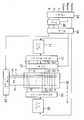
도 3의 플라즈마 디스플레이 장치는 플라즈마 디스플레이 패널(20), Y 전극 구동 회로(21), X 전극 구동 회로(22), 어드레스 전극 구동 회로(23), 식별 회로(24), 메모리(25), 제어 회로(26) 및 주사 회로(27)를 포함한다.The plasma display device of FIG. 3 includes a
식별 회로(24)에는 수직 동기 신호 Vsync, 수평 동기 신호 Hsync, 클럭 신호 Clock 및 데이터 신호로서 각각 8 비트의 RGB 신호가 공급된다. 식별 회로(24)는 수직 동기 신호 Vsync에 기초하여 메모리(25)에 RGB 데이터를 표시 데이터로서 기입한다. 제어 회로(26)는 Y 전극 구동 회로(21), X 전극 구동 회로(22), 어드레스 전극 구동 회로(23) 및 주사 회로(27)를 제어하여, 메모리(25)에 저장된 표시 데이터를 플라즈마 디스플레이 패널(20)에 표시한다. 이 때, 주사 회로(27)가 Y 전극 Y1 내지 Yn을 주사하고, 어드레스 전극 구동 회로(23)가 어드레스 전극 A1 내지 An을 구동시킴으로써, 데이터를 플라즈마 디스플레이 패널(20)에 기입하기 위한 기입 방전이 행해진다. 또한 Y 전극 구동 회로(21) 및 X 전극 구동 회로(22)에 의해 데이터가 기입된 표시 셀에서, Y 전극 Y1 내지 Yn 및 X 전극 X1 내지 Xn 사이에 유지 방전이 생성된다.The
도 3에 나타낸 종래의 구성에서는, Y 전극 구동 회로(21)로부터 주사 회로(27)로 연장되어 Y 전극 Y1 내지 Yn에 연결되는 선 y1 내지 yn은 Y 전극 구동 회로(21)와 주사 회로(27) 사이에서 상이한 배선 경로를 통해 상이한 배선 길이를 갖는다. 예를 들면 도 3의 예에서는, 또한 마찬가지로 X 전극 구동 회로(22)로부터 플라즈마 디스플레이 패널(20)로 연장되는 X 전극 X1 내지 Xn은 상이한 배선 경 로를 통해 상이한 배선 길이를 갖는다. 긴 배선 길이를 갖는 선 y1 및 그것에 접속되는 Y 전극 Y1은 비교적 짧은 배선 길이를 갖는 선 y3 및 그것에 접속되는 Y 전극 Y3과 비교하면, 배선 저항 및 배선 인덕턴스가 크다. 마찬가지로, 긴 배선 길이를 갖는 X 전극 X1은 비교적으로 짧은 배선 길이를 갖는 X 전극 X3과 비교하면, 배선 저항 및 배선 인덕턴스가 크다. 특히 배선 인덕턴스의 영향이 크고, Y 전극 Y1 내지 Yn 및 X 전극 X1 내지 Xn 사이에서 방전을 발생시킬 때에 각 배선·전극에 전류가 흐르면, 배선·전극에 따른 전압 강하가 생긴다. 이렇게 해서 생기는 전압 강하는 각 배선·전극에 따라 상이한 것이 된다.In the conventional configuration shown in FIG. 3, the lines y1 to yn extending from the Y
이 전압 강하의 결과, 전압 강하의 큰 전극에 있어서 플라즈마 디스플레이 패널의 방전 전압에 충분한 마진을 확보할 수 없게 되면, 방전 셀을 점등시키기 위해 필요한 전압을 공급할 수 없게 되는 경우가 있다. 이러한 경우, 화면의 깜빡임등이 생겨 표시 화질이 열화된다.As a result of this voltage drop, if a margin sufficient for the discharge voltage of the plasma display panel cannot be secured at the large electrode of the voltage drop, it may be impossible to supply a voltage necessary for lighting the discharge cell. In such a case, flickering or the like of the screen occurs, and the display quality deteriorates.
이상을 감안하여, 본 발명은 배선 길이에 따라 생기는 전압 강하를 저감시킨 플라즈마 디스플레이 패널을 제공하는 것을 목적으로 한다. 또한 배선 길이에 따라 생기는 전압 강하의 변동을 억제하여, 화질을 향상시킨 플라즈마 디스플레이 패널을 제공하는 것을 목적으로 한다.In view of the above, an object of this invention is to provide the plasma display panel which reduced the voltage drop which arises with wiring length. It is also an object of the present invention to provide a plasma display panel in which the variation in voltage drop caused by the wiring length is suppressed and the image quality is improved.
본 발명에 따른 플라즈마 디스플레이 장치는, 복수의 제1 전극과, 그 복수의 제1 전극에 대략 병행하게 배치되며 그 복수의 제1 전극 사이에 방전을 발생시키는 복수의 제2 전극과, 그 복수의 제1 전극에 방전 전압을 인가하는 제1 구동 회로와, 그 복수의 제2 전극에 방전 전압을 인가하는 제2 구동 회로와, 그 제1 및 제2 구동 회로와 그 제1 및 제2 전극 사이의 배선의 경로에 설치되고, 그 배선에 따른 전압 강하의 변동을 저감시키는 전압 변동 밸런스 유닛을 포함하고, 이 전압 변동 밸런스 유닛은 상기 배선에 중첩되도록 배치되는 도전판층을 포함하며, 그 배선에 흐르는 전류에 따라 그 도전판층에 생기는 와전류에 의해 상기 전압 강하의 변동을 저감시킨다.A plasma display device according to the present invention includes a plurality of first electrodes, a plurality of second electrodes disposed substantially in parallel to the plurality of first electrodes, and generating a discharge between the plurality of first electrodes, and the plurality of first electrodes. A first drive circuit for applying a discharge voltage to the first electrode, a second drive circuit for applying a discharge voltage to the plurality of second electrodes, and between the first and second drive circuits and the first and second electrodes A voltage fluctuation balance unit which is provided in a path of wiring of the wiring and reduces a fluctuation in voltage drop along the wiring, wherein the voltage fluctuating balance unit includes a conductive plate layer disposed to overlap the wiring, The variation in the voltage drop is reduced by the eddy current generated in the conductive plate layer in accordance with the current.
또한, 상기 전압 변동 밸런스 유닛은, 상기 배선 중 적어도 하나의 배선에 따라 배치되는 역전류선을 포함하며, 적어도 하나의 배선에 흐르는 전류와 역방향으로 흐르는 전류를 그 역전류선에 공급함으로써 상기 전압 강하의 변동을 저감시킨다.The voltage fluctuation balance unit further includes a reverse current line arranged along at least one of the wirings, and changes the voltage drop by supplying a current flowing in the reverse direction to a current flowing in at least one wiring to the reverse current line. Reduce.
또한, 상기 전압 변동 밸런스 유닛은, 상기 배선 중 적어도 하나의 배선에 인가되는 전압과 동일한 방향의 전압을 적어도 하나의 배선에 가산적으로 인가함으로써 상기 전압 강하의 변동을 저감시킨다.In addition, the voltage fluctuation balance unit reduces the fluctuation in the voltage drop by additionally applying a voltage in the same direction as the voltage applied to at least one of the wirings to the at least one wiring.
이들 구성에 의해 배선 길이에 따라 생기는 전압 강하의 변동을 억제하여, 화질을 향상시킨 플라즈마 디스플레이 패널 장치를 제공할 수 있다.These configurations can provide a plasma display panel device in which the fluctuation in voltage drop caused by the wiring length is suppressed and the image quality is improved.
또한 본 발명의 다른 측면에 따르면, 플라즈마 디스플레이 장치는 복수의 제1 전극과, 그 복수의 제1 전극에 대략 병행하게 배치되며 그 복수의 제1 전극 사이에 방전을 발생시키는 복수의 제2 전극과, 그 복수의 제1 전극의 기수번째의 전극에 방전 전압을 인가하는 제1 구동 회로와, 그 복수의 제1 전극의 우수번째의 전극에 방전 전압을 인가하는 제2 구동 회로를 포함하며, 그 제1 구동 회로와 그 제2 구동 회로와는 상호 대칭인 입출력 핀 배열을 갖는 것을 특징으로 한다.In addition, according to another aspect of the present invention, a plasma display device includes a plurality of first electrodes, a plurality of second electrodes disposed substantially in parallel with the plurality of first electrodes, and generating discharge between the plurality of first electrodes; And a first driving circuit for applying a discharge voltage to the odd-numbered electrodes of the plurality of first electrodes, and a second driving circuit for applying a discharge voltage to the even-numbered electrodes of the plurality of first electrodes. And an input / output pin arrangement that is symmetrical with the first driving circuit and the second driving circuit.
이와 같이 대칭적인 핀 배치로 함으로써, 배선을 균형있게 레이아웃하는 것이 가능하게 되어, 배선 인덕턴스에 의한 전압 강하를 효율적으로 저감시켜 전압 강하의 밸런스를 취하는 것이 용이해진다.The symmetrical pin arrangement makes it possible to lay out the wiring in a balanced manner, thereby effectively reducing the voltage drop due to the wiring inductance and making it easy to balance the voltage drop.
또한 본 발명의 다른 측면에 따르면, 플라즈마 디스플레이 장치는 복수의 제1 전극과, 그 복수의 제1 전극에 대략 병행하게 배치되며 그 복수의 제1 전극과의 사이에 방전을 발생시키는 복수의 제2 전극과, 기수번째의 그 제1 전극에 대하여 고전압을 공급하기 위한 기수 전극 H 사이드 구동 회로와 우수번째의 그 제1 전극에 대하여 저전압을 공급하기 위한 우수 전극 L 사이드 구동 회로를 집적화한 제1 집적 회로와, 기수번째의 그 제1 전극에 대하여 저전압을 공급하기 위한 기수 전극 L 사이드 구동 회로와 우수번째의 그 제1 전극에 대하여 고전압을 공급하기 위한 우수 전극 H 사이드 구동 회로를 집적화한 제2 집적 회로를 구비한 것을 특징으로 한다.In addition, according to another aspect of the present invention, the plasma display device includes a plurality of first electrodes and a plurality of second electrodes disposed substantially in parallel to the plurality of first electrodes and generating discharge between the plurality of first electrodes. First integration integrating an electrode, an odd electrode H side driving circuit for supplying a high voltage to the odd first electrode, and an even electrode L side driving circuit for supplying a low voltage to the even-numbered first electrode; A second integrated circuit integrating a circuit and an odd electrode L side driving circuit for supplying a low voltage to the odd-numbered first electrode and an even electrode H side driving circuit for supplying a high voltage to the even-numbered first electrode; A circuit is provided.
상기 발명에서는 각 전극 구동 회로를 H 사이드와 L 사이드로 분할하여, 인접하는 배선에 흐르는 전류가 각 방전 타이밍에서 역방향이 되도록, 각 전극 구동 회로와 배선을 배치한다. 이에 따라, 배선 인덕턴스의 영향을 삭감할 수 있다.In the above invention, each electrode driving circuit is divided into an H side and an L side, and the electrode driving circuit and the wiring are arranged so that the current flowing in the adjacent wiring is reversed at each discharge timing. Thereby, the influence of wiring inductance can be reduced.
또한 본 발명의 다른 측면에 따르면, 플라즈마 디스플레이 장치는 복수의 제1 전극과, 그 복수의 제1 전극에 대략 병행하게 배치되며 그 복수의 제1 전극 사이에 방전을 발생시키는 복수의 제2 전극을 구비한 플라즈마 디스플레이 장치로서, 그 복수의 제1 전극은 복수의 블록으로 분할되고, 그 각 블록에서 기수번째의 그 제1 전극을 구동시키기 위한 기수 전극 구동 회로와, 우수번째의 제1 전극을 구동시키기 위한 우수 전극 구동 회로를 각각 구비하는 것을 특징으로 한다.According to another aspect of the present invention, a plasma display device includes a plurality of first electrodes and a plurality of second electrodes disposed substantially in parallel with the plurality of first electrodes and generating discharge between the plurality of first electrodes. A plasma display device comprising: a plurality of first electrodes divided into a plurality of blocks, and a radix electrode driving circuit for driving the odd first electrode in each block, and the even first electrode It is characterized by comprising an excellent electrode driving circuit for each.
상기 발명에서는 각 전극 구동 회로를 복수로 분할하여, 인접하는 배선에 흐르는 전류가 각 방전 타이밍에서 역방향이 되도록 각 전극 구동 회로와 배선을 배치한다. 이에 따라, 배선 인덕턴스의 영향을 삭감시킬 수 있게 된다.In the above invention, each electrode driving circuit is divided into a plurality, and each electrode driving circuit and wiring are arranged so that the current flowing in the adjacent wiring is reversed at each discharge timing. As a result, the influence of the wiring inductance can be reduced.
이하에 첨부 도면을 이용하여, 본 발명의 실시예를 상세히 설명한다.EMBODIMENT OF THE INVENTION Hereinafter, the Example of this invention is described in detail using an accompanying drawing.
도 4는 본 발명에 따른 플라즈마 디스플레이 장치의 구성을 나타내는 도면이다. 도 4에서, 도 3과 동일한 요소는 동일한 번호를 부여한다.4 is a diagram illustrating a configuration of a plasma display device according to the present invention. In FIG. 4, the same elements as in FIG. 3 are given the same numbers.
도 4의 플라즈마 디스플레이 장치는 플라즈마 디스플레이 패널(20), Y 전극 구동 회로(21), X 전극 구동 회로(22), 어드레스 전극 구동 회로(23), 식별 회로(24), 메모리(25), 제어 회로(26), 주사 회로(27), 및 전압 변동 밸런스 유닛(31 및 32)을 포함한다.The plasma display device of FIG. 4 includes a
식별 회로(24)에는 수직 동기 신호 Vsync, 수평 동기 신호 Hsync, 클럭 신호 Clock 및 데이터 신호로서 각각 8 비트의 RGB 신호가 공급된다. 식별 회로(24)는 수직 동기 신호 Vsync에 기초하여 메모리(25)에 RGB 데이터를 표시 데이터로서 기입한다. 제어 회로(26)는 Y 전극 구동 회로(21), X 전극 구동 회로(22), 어드레스 전극 구동 회로(23) 및 주사 회로(27)를 제어하여, 메모리(25)에 저장된 표시 데이터를 플라즈마 디스플레이 패널(20)에 표시한다. 이 때, 주사 회로(27)가 Y 전극 Y1 내지 Yn을 주사하고, 어드레스 전극 구동 회로(23)가 어드레스 전극 Al 내지 An을 구동시킴으로써, 데이터를 플라즈마 디스플레이 패널(20)에 기입하기 위한 기입 방전이 행해진다. 또한 Y 전극 구동 회로(21) 및 X 전극 구동 회로(22)에 의해 데이터가 기입된 표시 셀에서, Y 전극 Y1 내지 Yn 및 X 전극 X1 내지 Xn 사이에 유지 방전이 생성된다.The
전압 변동 밸런스 유닛(31 및 32)은 각각 Y 전극 Y1 내지 Yn 및 X 전극 X1 내지 Xn에 관하여, 배선에 의한 전압 강하를 배선간에서 균일해지도록 배선 인덕턴스 등을 조정한다.The voltage
이하에, 전압 변동 밸런스 유닛(31 및 32)의 실시예를 설명한다.An embodiment of the voltage
도 5의 (a) 및 (b)는 전압 변동 밸런스 유닛의 제1 실시예의 구성을 나타내는 도면이다. 전압 변동 밸런스 유닛(31 또는 32)은 배선 S1 내지 S5 및 도전판(35)을 포함한다. Y 전극 Y1 내지 Yn용의 전압 변동 밸런스 유닛(31)의 경우에는, 배선 S1 내지 S5는 주사 회로(27)를 통해 Y 전극 Y1 내지 Yn에 연결되는 배선 y1 내지 yn이다. 또한 X 전극 X1 내지 Xn용의 전압 변동 밸런스 유닛(32)의 경우에는, 배선 S1 내지 S5는 X 전극 X1 내지 Xn이다. 또 도면을 간결하게 하기 위해 배선은 5개로 도시하고 있지만, 실제로는 도시되는 5개의 배선 각각은 복수의 선이 통합된 것이다. 따라서 전체적으로는 플라즈마 디스플레이 패널(20)의 Y 전극 혹은 X 전극의 수만큼의 배선이 전압 변동 밸런스 유닛(31 또는 32)에 설치된다.5A and 5B are diagrams showing the configuration of the first embodiment of the voltage fluctuation balance unit. The voltage
도 5의 (b)는 전압 변동 밸런스 유닛(31 또는 32)의 일부 층 구조를 나타내는 도면이다. 도 5의 (b)에 도시된 바와 같이 전압 변동 밸런스 유닛(31 또는 32)은 프린트 기판 상에 형성된 적어도 하나의 배선층(36)과 와전류층(37)을 포함한 다. 적어도 하나의 배선층(36)에는 배선(도 5의 (b)에서는 예를 들면 S1 및 S2)이 배치되고, 와전류층(37)에는 도전판(35)이 설치된다. 도전판(35)은 예를 들면 구리 등의 도전체로 형성되며, 배선에 전류가 흐르면 그 전류가 생성하는 자계를 상쇄하는 방향으로 와전류가 생성된다.FIG. 5B is a diagram showing a partial layer structure of the voltage
이 와전류가, 도 5의 (a)에 모식적으로 화살표로 나타내어진다. 도 5의 (a)에서 배선 S1 내지 S5에 흐르는 전류의 방향이 반대가 되는 경우에는(유지 방전시에는 전류의 방향은 순차 교체함), 모식적으로 나타내어지는 와전류의 방향도 당연히 역전된다.This eddy current is shown by the arrow typically in FIG.5 (a). In Fig. 5A, when the directions of the currents flowing through the wirings S1 to S5 are reversed (the directions of the currents are sequentially changed at the time of sustain discharge), the direction of the eddy current shown schematically is naturally reversed.
배선에 전류가 흐르고, 전류가 생성하는 자계를 상쇄하는 방향으로 와전류가 생기면, 그 배선의 배선 인덕턴스가 저감된다. 이 배선 인덕턴스 저감의 효과는 배선이 길수록 크다. 따라서, 비교적 긴 배선 길이를 갖는 배선은 배선 인덕턴스가 크게 저감되고, 비교적 짧은 배선 길이를 갖는 배선은 배선 인덕턴스가 그 정도로는 저감되지 않는다. 그에 따라, 배선 길이가 길수록 큰 값을 갖는 배선 인덕턴스를 배선 길이가 길수록 크게 저감시킬 수 있어, 결과적으로 각 배선의 배선 인덕턴스에 의한 전압 강하를 대략 균일하게 할 수 있다.When an electric current flows in a wiring and an eddy current is generated in the direction to cancel the magnetic field which the electric current produces | generates, the wiring inductance of the wiring is reduced. The longer the wiring inductance is, the greater the effect. Therefore, the wiring inductance of the wiring having a relatively long wiring length is greatly reduced, and the wiring inductance of the wiring having a relatively short wiring length is not so reduced. As a result, the longer the wiring length, the larger the wiring inductance having a larger value can be reduced, and as a result, the voltage drop due to the wiring inductance of each wiring can be made substantially uniform.
이와 같이 제1 실시예의 전압 변동 밸런스 유닛에 따르면, 와전류를 생성하는 도전판의 효과에 따라 각 배선의 배선 인덕턴스를 배선 길이에 따라 저감시킬 수 있어, 배선 인덕턴스에 의한 전압 강하를 대략 균일하게 조정할 수 있다.Thus, according to the voltage fluctuation balance unit of the first embodiment, the wiring inductance of each wiring can be reduced according to the wiring length according to the effect of the conductive plate generating the eddy current, so that the voltage drop caused by the wiring inductance can be adjusted approximately uniformly. have.
또 배선 S1 내지 S5의 배선 패턴은 도 5의 (a)에 도시된 바와 같이 중심으로부터 대칭으로 연장되는 형태일 필요는 없으며, 임의의 형상이라도 무방하다. 도 6은 전압 변동 밸런스 유닛의 제1 실시예의 다른 예를 나타내는 도면이고, 도 6에 도시된 바와 같이 배선 S1 내지 S5의 배선 패턴은 한쪽으로 연장하는 형상이라도 상관없다. 이들의 예로 나타낸 바와 같이, 본 발명에서 이 배선 패턴의 형상은 특정한 패턴에 한정되는 것이 아니다.The wiring patterns of the wirings S1 to S5 do not have to be symmetrically extended from the center as shown in Fig. 5A, and may be any shape. FIG. 6 is a view showing another example of the first embodiment of the voltage fluctuation balancing unit, and as shown in FIG. 6, the wiring patterns of the wirings S1 to S5 may be shaped to extend to one side. As shown in these examples, the shape of the wiring pattern in the present invention is not limited to a specific pattern.
도 7은 전압 변동 밸런스 유닛의 제2 실시예의 구성을 나타내는 도면이다.7 is a diagram illustrating a configuration of a second embodiment of the voltage fluctuation balance unit.
전압 변동 밸런스 유닛(31 또는 32)은 배선 S1 및 S2, 역전류선(41), 및 역전류 공급 유닛(42)을 포함한다. Y 전극 Y1 내지 Yn용의 전압 변동 밸런스 유닛(31)의 경우에는 배선 S1 및 S2는 주사 회로(27)를 통해 Y 전극 Y1 내지 Yn에 연결되는 배선 y1 내지 yn이다. 또한 X 전극 X1 내지 Xn용의 전압 변동 밸런스 유닛(32)의 경우에는 배선 S1 및 S2는 X 전극 X1 내지 Xn이다. 또 도면을 간결하게 하기 위해 배선은 2개로 도시하고 있지만, 실제로는 도시되는 2개의 배선 각각은 복수의 선이 통합된 것이다. 따라서 전체적으로는 플라즈마 디스플레이 패널(20)의 Y 전극 혹은 X 전극의 수만큼의 배선이 전압 변동 밸런스 유닛(31 또는 32)에 설치된다.The voltage
역전류 공급 유닛(42)은 배선 S2에 흐르는 전류와 역방향으로 흐르는 전류를 역전류선(41)에 공급한다. 배선 S2에 흐르는 전류의 방향이 반대가 되는 경우에는(유지 방전시에는 전류의 방향은 순차 교체됨), 역전류 공급 유닛(42)이 역전류선(41)에 공급하는 전류의 방향은 역전된다.The reverse
배선 S2에 전류가 흐르고, 이 전류가 생성하는 자계를 상쇄하는 방향의 전류가 역전류선(41)에 흐르면, 배선 S2의 배선 인덕턴스가 저감된다. 따라서, 배선 S1에 비교하여 긴 배선 길이를 갖는 배선 S2에 대하여 배선 인덕턴스를 저감시켜, 각 배선의 배선 인덕턴스에 의한 전압 강하를 대략 균일하게 할 수 있다. 또 제1 실시예에서도 설명한 바와 같이, 본 발명에서 배선 패턴의 형상은 특정한 패턴으로 한정되는 것은 아니다.When a current flows in the wiring S2 and a current in the direction of canceling the magnetic field generated by this current flows in the reverse
도 8은 전압 변동 밸런스 유닛의 제3 실시예의 구성을 나타내는 도면이다.8 is a diagram illustrating a configuration of a third embodiment of the voltage variation balance unit.
전압 변동 밸런스 유닛(31 또는 32)은 배선 S1 및 S2 및 전압 가산 유닛(51)을 포함한다. Y 전극 Y1 내지 Yn 용의 전압 변동 밸런스 유닛(31)의 경우에는 배선 S1 및 S2는 주사 회로(27)를 통해 Y 전극 Y1 내지 Yn에 연결되는 배선 y1 내지 yn 이다. 또한 X 전극 X1 내지 Xn 용의 전압 변동 밸런스 유닛(32)의 경우에는 배선 S1 및 S2는 X 전극 X1 내지 Xn 이다. 또 도면을 간결하게 하기 위해 배선은 2개로서 도시하고 있지만, 실제로는 도시되는 2개의 배선 각각은 복수의 선이 통합된 것이다.The voltage
전압 가산 유닛(51)은 배선 S2에 인가되는 전압과 같은 방향으로, 부가적인 전압을 인가한다. 구체적으로는, 전압 가산 유닛(51)은 Y 전극 구동 회로(21) 혹은 X 전극 구동 회로(22)와 마찬가지로, 펄스 전압을 공급하는 전압원으로 구성되며, Y 전극 구동 회로(21) 혹은 X 전극 구동 회로(22)가 동작하는데 동기하여, 부가적인 전압을 발생시켜 이 전압을 가산한다. 배선 S1에 비교하여 긴 배선 길이를 갖는 배선 S2에서 부가적인 전압을 가산함으로써 배선 인덕턴스에 의한 전압 강하를 보상하여, 각 배선에서의 전압 강하를 대략 균일하게 할 수 있다. 또 본 발명에 있어서, 배선 패턴의 형상은 특정한 패턴에 한정되는 것은 아니다.The
도 9는 본 발명에 따른 플라즈마 디스플레이 장치의 다른 구성예를 나타내는 도면이다. 도 9에서, 도 4와 동일한 요소는 동일한 번호를 부여하고 그에 대한 설명은 생략한다.9 is a diagram showing another configuration example of the plasma display device according to the present invention. In FIG. 9, the same elements as in FIG. 4 are given the same numbers and description thereof will be omitted.
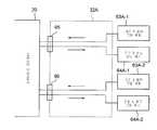
도 9의 플라즈마 디스플레이 장치는 플라즈마 디스플레이 패널(20), 기수 Y 전극 구동 회로(61), 우수 Y 전극 구동 회로(62), 기수 X 전극 구동 회로(63), 우수 X 전극 구동 회로(64), 어드레스 전극 구동 회로(23), 식별 회로(24), 메모리(25), 제어 회로(26), 주사 회로(27) 및 전압 변동 밸런스 유닛(31A 및 32A)을 포함한다. 도 9의 플라즈마 디스플레이 장치에서는, Y 전극 및 X 전극 각각에 대한 전극 구동 회로가 기수번째의 전극을 구동시키는 구동 회로와 우수번째의 전극을 구동시키는 구동 회로로 나뉘어지는 것을 특징으로 한다. 이러한 구성은, 도 2에 나타낸 ALIS 방식의 플라즈마 디스플레이 패널을 구동하는데 적합하다.The plasma display apparatus of FIG. 9 includes a
이하에, 전압 변동 밸런스 유닛(31A 및 32A)의 실시예를 설명한다.An embodiment of the voltage
도 10은 전압 변동 밸런스 유닛의 제4 실시예의 구성을 나타내는 도면이다.Fig. 10 is a diagram showing the configuration of the fourth embodiment of the voltage fluctuation balance unit.
전압 변동 밸런스 유닛(31A 또는 32A)은 배선 S1 내지 S4 및 도전판(71)을 포함한다. Y 전극 Y1 내지 Yn용의 전압 변동 밸런스 유닛(31A)의 경우에는, 배선 S1 내지 S4는 주사 회로(27)를 통해 Y 전극 Y1 내지 Yn에 연결되는 배선 y1 내지 yn이다. 또한 X 전극 X1 내지 Xn용의 전압 변동 밸런스 유닛(32A)의 경우에는, 배선 S1 내지 S4는 X 전극 X1 내지 Xn이다. 또 도면을 간결하게 하기 위해 배선은 4개로 도시하고 있지만, 실제로는 도시되는 4개의 배선 각각은 복수의 선이 통합된 것이다. 또한 배선 S1 및 S2는 기수번째의 전극에 대응하는 선이고, 배선 S3 및 S4는 우수번째의 전극에 대응하는 선이다.The voltage
도전판(71)은 예를 들면 구리 등의 도전체로 형성되고, 배선에 전류가 흐르면, 그 전류가 생성하는 자계를 상쇄하는 방향으로 와전류가 생성된다.The
배선에 전류가 흐르고, 전류가 생성하는 자계를 상쇄하는 방향으로 와전류가 생기면, 그 배선의 배선 인덕턴스가 저감된다. 이 배선 인덕턴스 저감의 효과는 배선이 길수록 크다. 따라서, 비교적 긴 배선 길이를 갖는 배선은 배선 인덕턴스가 크게 저감되며, 비교적 짧은 배선 길이를 갖는 배선은 배선 인덕턴스가 그 정도로는 저감되지 않는다. 그에 따라, 배선 길이가 길수록 큰 값을 갖는 배선 인덕턴스를 배선 길이가 길수록 크게 저감시킬 수 있고, 결과적으로 각 배선의 배선 인덕턴스에 의한 전압 강하를 대략 균일하게 할 수 있다.When an electric current flows in a wiring and an eddy current is generated in the direction to cancel the magnetic field which the electric current produces | generates, the wiring inductance of the wiring is reduced. The longer the wiring inductance is, the greater the effect. Therefore, the wiring inductance of the wiring having a relatively long wiring length is greatly reduced, and the wiring inductance of the wiring having a relatively short wiring length is not reduced to that extent. As a result, the longer the wiring length, the larger the wiring inductance having a larger value can be reduced, and as a result, the voltage drop due to the wiring inductance of each wiring can be made substantially uniform.
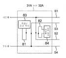
도 11은 전압 변동 밸런스 유닛의 제5 실시예의 구성을 나타내는 도면이다.11 is a diagram showing the configuration of the fifth embodiment of the voltage fluctuation balance unit.
전압 변동 밸런스 유닛(31A 또는 32A)은 배선 S1 내지 S4, 역전류선(81 및 82) 및 역전류 공급 유닛(83 및 84)을 포함한다. 배선 S1 및 S2는 기수번째의 전극에 대응하는 선이고, 배선 S3 및 S4는 우수번째의 전극에 대응하는 선이다. 또 도면을 간결하게 하기 위해 배선은 4개로 도시하고 있지만, 실제로는 도시되는 4개의 배선 각각은 복수의 선이 통합된 것이다.The voltage
역전류 공급 유닛(83)은 배선 S3에 흐르는 전류와 역방향으로 흐르는 전류를 역전류선(81)에 공급한다. 배선 S3에 흐르는 전류의 방향이 반대가 되는 경우에는(유지 방전시에는 전류의 방향은 순차 교체됨), 역전류 공급 유닛(83)이 역전류선(81)에 공급하는 전류의 방향은 역전된다. 또한 마찬가지로, 역전류 공급 유닛(84)은 배선 S2에 흐르는 전류와 역방향으로 흐르는 전류를 역전류선(82)에 공급한다.The reverse
배선 S2 및 S3에 전류가 흐르고, 이 전류가 생성하는 자계를 상쇄하는 방향의 전류가 역전류선에 흐르면, 배선 S2의 배선 인덕턴스가 저감된다. 따라서, 배선 S1 및 S4에 비교하여 긴 배선 길이를 갖는 배선 S2 및 S3에 대하여 배선 인덕턴스를 저감시켜, 각 배선의 배선 인덕턴스에 의한 전압 강하를 대략 균일하게 할 수 있다.When a current flows through the wirings S2 and S3 and a current in a direction to cancel the magnetic field generated by the current flows through the reverse current line, the wiring inductance of the wiring S2 is reduced. Therefore, the wiring inductance can be reduced for the wirings S2 and S3 having a longer wiring length as compared with the wirings S1 and S4, and the voltage drop due to the wiring inductance of each wiring can be made substantially uniform.
도 12는 전압 변동 밸런스 유닛의 제6 실시예의 구성을 나타내는 도면이다.Fig. 12 is a diagram showing the configuration of the sixth embodiment of the voltage fluctuation balance unit.
전압 변동 밸런스 유닛(31A 또는 32A)은 배선 S1 내지 S4, 및 전압 가산 유닛(91 및 92)을 포함한다. 배선 S1 및 S2는 기수번째의 전극에 대응하는 선이고, 배선 S3 및 S4는 우수번째의 전극에 대응하는 선이다. 또 도면을 간결하게 하기 위해 배선은 4개로서 도시하고 있지만, 실제로는 도시되는 4개의 배선 각각은 복수의 선이 통합된 것이다.The voltage
전압 가산 유닛(91)은 우수번째의 전극에 대응하는 배선 S3에 인가되는 전압과 동일한 방향으로 부가적인 전압을 인가한다. 구체적으로는 전압 가산 유닛(91)은 우수 Y 전극 구동 회로(62) 혹은 우수 X 전극 구동 회로(64)와 마찬가지로, 펄스 전압을 공급하는 전압원으로 구성되며, 우수 Y 전극 구동 회로(62) 혹은 우수 X 전극 구동 회로(64)가 동작하는데 동기하여, 부가적인 전압을 발생시켜 이 전압을 가산한다. 또한 마찬가지로, 전압 가산 유닛(92)은 기수번째의 전극에 대응하는 배선 S2에 인가되는 전압과 동일한 방향으로 부가적인 전압을 인가한다.The
배선 S1 및 S4에 비교하여 긴 배선 길이를 갖는 배선 S2 및 S3에 있어서, 부가적인 전압을 가산함으로써 배선 인덕턴스에 의한 전압 강하를 보상하여, 각 배선에서의 전압 강하를 대략 균일하게 할 수 있다.In the wirings S2 and S3 having a longer wiring length compared to the wirings S1 and S4, by adding additional voltages, the voltage drop due to the wiring inductance can be compensated, and the voltage drop in each wiring can be made substantially uniform.
도 13은, 도 12에 나타내여지는 전압 변동 밸런스 유닛의 제6 실시예의 상세한 구성을 나타내는 도면이다.FIG. 13 is a diagram showing a detailed configuration of a sixth embodiment of the voltage fluctuation balance unit shown in FIG.
도 13의 전압 변동 밸런스 유닛(31A 또는 32A)에서 전압 가산 유닛(91 및 92)은 스위치로 구성된다. 스위치의 한쪽 단자는 배선 S2 혹은 S3에 접속되고, 다른 단자는 전극 구동 회로의 전원 핀에 접속된다. 이 때, 우수번째의 전극에 대응하는 배선 S3에 전압 가산하는 전압 가산 유닛(91)은 기수 Y 전극 구동 회로(61) 또는 기수 X 전극 구동 회로(63)의 전원 핀에 접속되고, 기수번째의 전극에 대응하는 배선 S2에 전압 가산하는 전압 가산 유닛(92)은 우수 Y 전극 구동 회로(62) 또는 우수 X 전극 구동 회로(64)의 전원 핀에 접속된다.In the voltage
전압 변동 밸런스 유닛(31A)을 예로 하여 도 13의 구성의 동작을 이하에 설명한다.The operation of the configuration of FIG. 13 will be described below by taking the voltage
전압 변동 밸런스 유닛(31A)은 기수 Y 전극 구동 회로(61)와 우수 Y 전극 구동 회로(62)에 접속된다. 기수 Y 전극 구동 회로(61)는 전원 핀에 접속되는 컨덴서 C1로부터 소정의 타이밍에서 배선 S1 및 S2에 전압을 공급하고, 이 때 우수 Y 전극 구동 회로(62)는 구동되지 않는다. 또 이 때, X 전극측에서는 기수 X 전극 구동 회로(63)는 비구동이고, 우수 X 전극 구동 회로(64)가 구동하여 전압을 공급하고 있다. 이 방전이 종료하면, 다음 방전 타이밍에서 우수 Y 전극 구동 회로(62)가 전원 핀에 접속되는 컨덴서 C2로부터 배선 S3 및 S4에 전압을 공급하고, 이 때 기수 Y 전극 구동 회로(61)는 비구동 상태에 있다.The voltage
즉, 기수 Y 전극 구동 회로(61)가 구동하고 있을 때에는 우수 Y 전극 구동 회로(62)는 비구동이고, 반대로 우수 Y 전극 구동 회로(62)가 구동하고 있을 때에는 기수 Y 전극 구동 회로(61)는 비구동이다.That is, when the odd Y
이것을 이용하여, 도 13의 구성에서 기수 Y 전극 구동 회로(61)가 구동하고 있을 때에는 전압 가산 유닛(92)의 스위치를 도통하여 우수 Y 전극 구동 회로(62)의 전원 핀에 접속되어 있는 컨덴서 C2로부터 전하를 공급함으로써 전압 가산을 실행한다. 또한 반대로, 우수 Y 전극 구동 회로(62)가 구동하고 있을 때에는 전압 가산 유닛(91)의 스위치를 도통하여 기수 Y 전극 구동 회로(61)의 전원 핀에 접속되어 있는 컨덴서 C1로부터 전하를 공급함으로써 전압 가산을 실행한다.Using this, when the radix Y
이상의 동작에 의해 종래의 구성에서 사용되고 있는 전원 공급용의 컨덴서를 이용함으로써, 효율적으로 전압 가산 유닛을 실현할 수 있다.By the above operation, the voltage adding unit can be efficiently realized by using the power supply capacitor used in the conventional configuration.
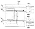
도 14는 전압 변동 밸런스 유닛의 제7 실시예의 구성을 나타내는 도면이다.Fig. 14 is a diagram showing the configuration of the seventh embodiment of the voltage fluctuation balance unit.
상기 설명한 바와 같이 기수 Y 전극 구동 회로(61)가 구동하고 있을 때에는 우수 Y 전극 구동 회로(62)는 구동하지 않는다. 이 때, 대향하는 X 전극측에서는 기수 X 전극 구동 회로(63)가 기수 Y 전극 구동 회로(61)로부터 공급되는 전압의 접지측이 되고, 우수 X 전극 구동 회로(64)가 구동하여 전압을 공급함으로써, 접지가 되는 우수 Y 전극 구동 회로(62)에 전류가 유입된다. 이와 같이 하여 방전이 실행되면, 이어서 기수 X 전극 구동 회로(63)로부터 비구동 상태인 기수 Y 전극 구 동 회로(61)에 전류가 흐르고, 구동 상태인 우수 Y 전극 구동 회로(62)로부터 우수 X 전극 구동 회로(64)에 전류가 흘러 방전이 실행된다.As described above, when the odd Y
이러한 동작을 이용하여, 도 14의 구성에서는 효율적으로 배선 인덕턴스에 의한 전압 강하를 막을 수 있다. 도 14에서는 X 전극측의 전압 변동 밸런스 유닛(32A)을 예로 들어, 전압 변동 밸런스 유닛의 제7 실시예의 구성을 나타내고 있다.By using this operation, the voltage drop caused by the wiring inductance can be effectively prevented in the configuration of FIG. In Fig. 14, the voltage
이 구성에서는 기수 X 전극 구동 회로(63)는 전압 공급측인 H 사이드 기수 X 전극 구동 회로(63-1)와 접지측인 L 사이드 기수 X 전극 구동 회로(63-2)로 분할되고, 우수 X 전극 구동 회로(64)는 전압 공급측인 H 사이드 우수 X 전극 구동 회로(64-1)와 접지측인 L 사이드 우수 X 전극 구동 회로(64-2)로 분할되어 있다.In this configuration, the radix X
임의의 방전 타이밍에서는 H 사이드 기수 X 전극 구동 회로(63-1)로부터 Y 전극측에 전류가 공급되고, L 사이드 우수 X 전극 구동 회로(64-2)에 Y 전극측으로부터 전류가 공급된다. 이 때의 전류의 흐름을 실선으로 나타내고 있다. 도 14로부터 알 수 있듯이, 인접하는 배선간에 전류의 방향이 반대가 되므로, 배선 인덕턴스에 의한 전압 강하를 삭감시킬 수 있다.At an arbitrary discharge timing, a current is supplied from the H side odd X electrode drive circuit 63-1 to the Y electrode side, and a current is supplied from the Y electrode side to the L side even X electrode drive circuit 64-2. The flow of electric current at this time is shown by the solid line. As can be seen from Fig. 14, since the direction of current is reversed between adjacent wirings, the voltage drop due to wiring inductance can be reduced.
또한 다음의 방전 타이밍에서는 H 사이드 우수 X 전극 구동 회로(64-1)로부터 Y 전극측에 전류가 공급되고, L 사이드 기수 X 전극 구동 회로(63-2)에 Y 전극측으로부터 전류가 공급된다. 이 때의 전류의 흐름을 점선으로 나타내고 있다. 도면으로부터 알 수 있듯이, 인접하는 배선간에 전류의 방향이 반대가 되기 때문에, 배선 인덕턴스에 의한 전압 강하를 삭감시킬 수 있게 된다.At the next discharge timing, a current is supplied from the H side even X electrode driving circuit 64-1 to the Y electrode side, and a current is supplied from the Y electrode side to the L side odd X electrode driving circuit 63-2. The current flow at this time is shown by the dotted line. As can be seen from the figure, since the direction of current is reversed between adjacent wirings, the voltage drop due to wiring inductance can be reduced.
이와 같이 전압 변동 밸런스 유닛의 제7 실시예에서는 각 전극 구동 회로를 H 사이드와 L 사이드로 분할하여, 인접하는 배선에 흐르는 전류가 각 방전 타이밍에서 역방향이 되도록 각 전극 구동 회로와 배선을 배치한다. 이에 따라, 배선 인덕턴스의 영향을 삭감시킬 수 있게 된다. 또 종래의 구성에서는 푸시풀 회로의 풀업측과 풀다운측에 해당하는 H 사이드와 L 사이드가 본래 하나의 세트로서 제공되기 때문에 전류의 흐름이 부분적으로 쌍방향이 되지 않아 인덕턴스가 증가할 우려가 있었다. 본 실시예에서는 각 전극 구동 회로를 H 사이드와 L 사이드로 분할함으로써, 완전한 쌍방향성을 실현하고 있다.As described above, in the seventh embodiment of the voltage fluctuation balancing unit, each electrode driving circuit is divided into the H side and the L side, and the electrode driving circuit and the wiring are arranged so that the current flowing in the adjacent wiring is reversed at each discharge timing. As a result, the influence of the wiring inductance can be reduced. In the conventional configuration, since the H side and the L side corresponding to the pull-up side and the pull-down side of the push-pull circuit are originally provided as a set, there is a concern that the inductance increases because the current flow does not partially become bidirectional. In this embodiment, each of the electrode drive circuits is divided into an H side and an L side to realize complete bidirectionality.
또 여기서는 X 전극측을 예로 들어 설명했지만, Y 전극측에 대해서도 동일한 구성이 가능한 것은 분명하다.In addition, although the X electrode side was demonstrated as an example here, it is clear that the same structure is also possible for the Y electrode side.
도 15는 전압 변동 밸런스 유닛의 제8 실시예의 구성을 나타내는 도면이다.Fig. 15 is a diagram showing the configuration of the eighth embodiment of the voltage fluctuation balance unit.
도 15에서는 X 전극측의 전압 변동 밸런스 유닛(32A)을 예로 들어, 전압 변동 밸런스 유닛의 제8 실시예의 구성을 나타내고 있다.In FIG. 15, the voltage
이 구성에서는 기수 X 전극 구동 회로(63)는 제1 기수 X 전극 구동 회로(63A-1)와 제2 기수 X 전극 구동 회로(63A-2)로 분할되고, 우수 X 전극 구동 회로(64)는 제1 우수 X 전극 구동 회로(64A-1)와 제2 우수 X 전극 구동 회로(64A-2)로 분할되어 있다. 도 15에서, 커넥터(95)는 플라즈마 디스플레이 표시 장치의 상반분의 모든 전극을 구동시키기 위한 배선에 대한 커넥터이고, 커넥터(96)는 플라즈마 디스플레이 표시 장치의 하반분의 모든 전극을 구동시키기 위한 배선에 대한 커넥터이다.In this configuration, the radix X
임의의 방전 타이밍에서는 기수 X 전극 구동 회로(63A-1 및 63A-2)로부터 Y 전극측에 전류가 공급되고, 우수 X 전극 구동 회로(64A-1 및 64A-2)에 Y 전극측으로부터 전류가 공급된다. 이 때의 전류의 흐름을 실선으로 나타내고 있다. 도 15로부터 알 수 있듯이, 인접하는 배선 사이에서 전류의 방향이 반대가 되기 때문에, 배선 인덕턴스에 의한 전압 강하를 삭감시킬 수 있게 된다. 이와 같이 각 전극 구동 회로를 복수로 분할하는 것은 플라즈마 디스플레이 패널(20)로 공급하는 전극의 커넥터 배치를 고려했을 때에 의미가 있다. 즉, 도 15에 도시된 바와 같이 커넥터 위치가 두개이면, 각 전극 구동 회로를 두개로 분할함으로써, 배선의 불필요한 인출을 없앰과 함께, 인접하는 배선의 전류의 방향을 반대로 하여, 배선 인덕턴스의 영향을 삭감시킬 수 있게 된다.At an arbitrary discharge timing, a current is supplied from the radix X
이와 같이 전압 변동 밸런스 유닛의 제7 실시예에서는 각 전극 구동 회로를 복수로 분할하여, 인접하는 배선에 흐르는 전류가 각 방전 타이밍에 있어서 역방향이 되도록 각 전극 구동 회로와 배선을 배치한다. 이에 따라, 배선 인덕턴스의 영향을 삭감시킬 수 있게 된다.As described above, in the seventh embodiment of the voltage fluctuation balancing unit, each electrode driving circuit is divided into a plurality, and the electrode driving circuit and the wiring are arranged so that the current flowing in the adjacent wiring is reversed at each discharge timing. As a result, the influence of the wiring inductance can be reduced.
또 여기서는 X 전극측을 예로 들어 설명했지만, Y 전극측에 대해서도 동일한 구성이 가능한 것은 분명하다.In addition, although the X electrode side was demonstrated as an example here, it is clear that the same structure is also possible for the Y electrode side.
도 16은 기수 X 전극 구동 회로(63) 및 우수 X 전극 구동 회로(64)의 구성을 나타낸 회로도이다.FIG. 16 is a circuit diagram showing the configurations of the radix X
도 16의 기수 X 전극 구동 회로(63)는 파워 모듈 혹은 하이브리드 IC를 이용하여 구성되는 것으로, L 사이드 입력 핀(101), H 사이드 입력 핀(102), 접지 핀(103), L 사이드 출력 핀(104), H 사이드 출력 핀(105), 전원 핀(106), 스위치 소자(107 및 108) 및 구동 회로(109 및 110)를 포함한다. 또한 우수 X 전극 구동 회로(64)는 파워 모듈 혹은 하이브리드 IC를 이용하여 구성되는 것으로, L 사이드 입력 핀(201), H 사이드 입력 핀(202), 접지 핀(203), L 사이드 출력 핀(204), H 사이드 출력 핀(205), 전원 핀(206), 스위치 소자(207 및 208) 및 구동 회로(209 및 210)를 포함한다.The base X
본 발명의 기수 X 전극 구동 회로(63) 및 우수 X 전극 구동 회로(64)는 도 16에 도시된 바와 같이 기수 X 전극 구동 회로(63)와 우수 X 전극 구동 회로(64) 사이에서 각 핀이 대칭적인 공간 배치로 되어 있는 것을 특징으로 한다. 즉, 기수 X 전극 구동 회로(63)에서는 접지 핀이 최상부에 있고 다음이 L 사이드 출력 핀으로 되어 있는데 비해 우수 X 전극 구동 회로(64)에서는 접지 핀은 최하부에 있고 다음이 L 사이드 출력 핀으로 되어 있다.The odd-numbered X
이와 같이 대칭적인 핀 배치로 함으로써, 전압 변동 밸런스 유닛(32A)에서의 배선을 균형있게 레이아웃할 수 있고, 배선 인덕턴스에 의한 전압 강하를 효율적으로 저감하여 전압 강하의 균형을 잡는 것이 용이해진다. 또한 컨덴서 C1 및 C2사이의 전하의 이동을 용이하게 함으로써, 전압 변동을 저감시키는 효과를 얻을 수 있다.By adopting the symmetrical pin arrangement in this way, the wiring in the voltage
이상, 본 발명을 실시예에 기초하여 설명했지만, 본 발명은 상기 실시예에 한정되는 것은 아니며, 특허 청구의 범위에 기재된 범위 내에서 여러가지 변형이 가능하다.As mentioned above, although this invention was demonstrated based on the Example, this invention is not limited to the said Example, A various deformation | transformation is possible within the range of a claim.
전술한 바와 같이, 본 발명에서는 배선 인덕턴스에 의한 전압 강하를 저감시키기 위해 전압 변동 밸런스 유닛을 설치한다. 이 전압 변동 밸런스 유닛은, 배선에 중첩되도록 배치되는 도전판층이고, 배선에 흐르는 전류에 따라 도전판층에 생기는 와전류에 의해 전압 강하의 변동을 저감시킬 수 있다. 또한, 전압 변동 밸런스 유닛은 배선에 따라 배치되는 역전류선에 역방향 전류를 공급함으로써, 전압 강하의 변동을 저감시킬 수 있다. 또한, 전압 변동 밸런스 유닛은 배선에 인가되는 전압과 동일한 방향의 전압을 가산적으로 인가함으로써, 전압 강하의 변동을 저감시킬 수 있다.As described above, in the present invention, a voltage fluctuation balance unit is provided in order to reduce the voltage drop caused by the wiring inductance. This voltage fluctuation balance unit is a conductive plate layer which is arrange | positioned so that it may overlap with wiring, and can reduce the fluctuation | variation of a voltage drop by the eddy current which arises in a conductive plate layer according to the electric current which flows in a wiring. In addition, the voltage fluctuation balance unit can reduce fluctuations in voltage drop by supplying reverse current to the reverse current lines arranged along the wiring. In addition, the voltage fluctuation balance unit can additionally reduce voltage fluctuation by additionally applying a voltage in the same direction as the voltage applied to the wiring.
이들 구성에 의해, 배선 길이에 따라 생기는 전압 강하의 변동을 억제하고, 화질을 향상시킨 플라즈마 디스플레이 패널 장치를 제공할 수 있다.With these configurations, it is possible to provide a plasma display panel device in which variation in voltage drop caused by wiring length is suppressed and image quality is improved.
Claims (6)
Translated fromKoreanApplications Claiming Priority (2)
| Application Number | Priority Date | Filing Date | Title |
|---|---|---|---|
| JP2000391389AJP2002196719A (en) | 2000-12-22 | 2000-12-22 | Plasma display device |
| JPJP-P-2000-00391389 | 2000-12-22 |
Related Child Applications (1)
| Application Number | Title | Priority Date | Filing Date |
|---|---|---|---|
| KR1020070121642ADivisionKR100798573B1 (en) | 2000-12-22 | 2007-11-27 | Plasma display device |
Publications (2)
| Publication Number | Publication Date |
|---|---|
| KR20020051822A KR20020051822A (en) | 2002-06-29 |
| KR100829323B1true KR100829323B1 (en) | 2008-05-13 |
Family
ID=18857536
Family Applications (2)
| Application Number | Title | Priority Date | Filing Date |
|---|---|---|---|
| KR1020010074142AExpired - Fee RelatedKR100829323B1 (en) | 2000-12-22 | 2001-11-27 | Plasma display apparatus |
| KR1020070121642AExpired - Fee RelatedKR100798573B1 (en) | 2000-12-22 | 2007-11-27 | Plasma display device |
Family Applications After (1)
| Application Number | Title | Priority Date | Filing Date |
|---|---|---|---|
| KR1020070121642AExpired - Fee RelatedKR100798573B1 (en) | 2000-12-22 | 2007-11-27 | Plasma display device |
Country Status (5)
| Country | Link |
|---|---|
| US (1) | US6538389B2 (en) |
| EP (1) | EP1221685A3 (en) |
| JP (1) | JP2002196719A (en) |
| KR (2) | KR100829323B1 (en) |
| TW (1) | TW535129B (en) |
Cited By (1)
| Publication number | Priority date | Publication date | Assignee | Title |
|---|---|---|---|---|
| KR101173597B1 (en) | 2010-08-23 | 2012-08-13 | 주식회사 신창전기 | Mirror Switch Integrated with Folding Switch for Vehicle |
Families Citing this family (10)
| Publication number | Priority date | Publication date | Assignee | Title |
|---|---|---|---|---|
| JP2003045338A (en)* | 2001-07-30 | 2003-02-14 | Nec Corp | Plasma display device |
| US7283687B2 (en)* | 2001-09-24 | 2007-10-16 | International Business Machines Corporation | Imaging for virtual cameras |
| JP2004184682A (en)* | 2002-12-03 | 2004-07-02 | Fujitsu Hitachi Plasma Display Ltd | Plasma display device |
| JPWO2007000802A1 (en)* | 2005-06-27 | 2009-01-22 | 日立プラズマディスプレイ株式会社 | Plasma display device |
| KR101088288B1 (en)* | 2007-04-25 | 2011-11-30 | 파나소닉 주식회사 | Plasma display device |
| US20100141558A1 (en)* | 2008-06-10 | 2010-06-10 | Samsung Sdi Co., Ltd | Plasma display device |
| TWI406260B (en) | 2010-12-29 | 2013-08-21 | Au Optronics Corp | Control circuit with voltage charge sharing function of display panel and control method of same |
| JP6660846B2 (en) | 2016-08-01 | 2020-03-11 | 株式会社ジャパンディスプレイ | Input detection device and electronic device |
| TWI643113B (en)* | 2017-03-03 | 2018-12-01 | 日商阿爾普士電氣股份有限公司 | Input device and control method thereof |
| CN113594204B (en)* | 2020-04-30 | 2024-04-02 | 京东方科技集团股份有限公司 | Display substrate and preparation method thereof, display device |
Citations (9)
| Publication number | Priority date | Publication date | Assignee | Title |
|---|---|---|---|---|
| JPH0720438A (en)* | 1993-07-02 | 1995-01-24 | Sharp Corp | Controller with voltage correction function |
| JPH0764508A (en)* | 1993-08-30 | 1995-03-10 | Fujitsu General Ltd | Display panel driving method and device thereof |
| JPH0772833A (en)* | 1993-07-06 | 1995-03-17 | Sharp Corp | Voltage compensation circuit and display device |
| JPH08248912A (en)* | 1995-03-15 | 1996-09-27 | Canon Inc | Energization control method for image forming apparatus and energization apparatus |
| JPH08248921A (en)* | 1994-06-08 | 1996-09-27 | Canon Inc | Electron beam generator and image forming apparatus using the same |
| KR19980064635A (en)* | 1996-12-25 | 1998-10-07 | 가네꼬히사시 | Surface Discharge Plasma Display Device |
| KR19990029152A (en)* | 1997-09-01 | 1999-04-26 | 이데이 노부유끼 | Plasma display |
| KR19990072298A (en)* | 1998-01-27 | 1999-09-27 | 하라 세이지 | Wiring board, semiconductor device, electronic device, and circuit board for electronic parts |
| JP2000330514A (en)* | 1999-05-20 | 2000-11-30 | Hitachi Ltd | Display device, PDP display device and driving circuit thereof |
Family Cites Families (10)
| Publication number | Priority date | Publication date | Assignee | Title |
|---|---|---|---|---|
| JP2801893B2 (en) | 1995-08-03 | 1998-09-21 | 富士通株式会社 | Plasma display panel driving method and plasma display device |
| JP3458997B2 (en) | 1997-08-21 | 2003-10-20 | 日本ビクター株式会社 | Plasma display panel display device and driving method thereof |
| JP4210805B2 (en)* | 1998-06-05 | 2009-01-21 | 株式会社日立プラズマパテントライセンシング | Driving method of gas discharge device |
| JP3289684B2 (en)* | 1998-09-11 | 2002-06-10 | 日本電気株式会社 | Plasma display panel, plasma display module and driving method thereof |
| JP3266191B2 (en)* | 1998-12-25 | 2002-03-18 | 日本電気株式会社 | Plasma display and its image display method |
| JP4294141B2 (en)* | 1999-01-27 | 2009-07-08 | 株式会社日立製作所 | Display device |
| GB9902343D0 (en)* | 1999-02-04 | 1999-03-24 | Sharp Kk | overnment Of The United Kingdom Of Great Britain And Northern Ireland The Addressable matrix arrays |
| JP2000250425A (en)* | 1999-02-25 | 2000-09-14 | Fujitsu Ltd | Driver IC mounting module |
| US6320326B1 (en)* | 1999-04-08 | 2001-11-20 | Matsushita Electric Industrial Co., Ltd. | AC plasma display apparatus |
| KR100295455B1 (en)* | 1999-06-15 | 2001-07-12 | 구자홍 | Apparatus And Method For Detach Voltage of PDP |
- 2000
- 2000-12-22JPJP2000391389Apatent/JP2002196719A/enactivePending
- 2001
- 2001-11-19USUS09/988,160patent/US6538389B2/ennot_activeExpired - Fee Related
- 2001-11-21EPEP01309811Apatent/EP1221685A3/ennot_activeWithdrawn
- 2001-11-22TWTW090128964Apatent/TW535129B/ennot_activeIP Right Cessation
- 2001-11-27KRKR1020010074142Apatent/KR100829323B1/ennot_activeExpired - Fee Related
- 2007
- 2007-11-27KRKR1020070121642Apatent/KR100798573B1/ennot_activeExpired - Fee Related
Patent Citations (9)
| Publication number | Priority date | Publication date | Assignee | Title |
|---|---|---|---|---|
| JPH0720438A (en)* | 1993-07-02 | 1995-01-24 | Sharp Corp | Controller with voltage correction function |
| JPH0772833A (en)* | 1993-07-06 | 1995-03-17 | Sharp Corp | Voltage compensation circuit and display device |
| JPH0764508A (en)* | 1993-08-30 | 1995-03-10 | Fujitsu General Ltd | Display panel driving method and device thereof |
| JPH08248921A (en)* | 1994-06-08 | 1996-09-27 | Canon Inc | Electron beam generator and image forming apparatus using the same |
| JPH08248912A (en)* | 1995-03-15 | 1996-09-27 | Canon Inc | Energization control method for image forming apparatus and energization apparatus |
| KR19980064635A (en)* | 1996-12-25 | 1998-10-07 | 가네꼬히사시 | Surface Discharge Plasma Display Device |
| KR19990029152A (en)* | 1997-09-01 | 1999-04-26 | 이데이 노부유끼 | Plasma display |
| KR19990072298A (en)* | 1998-01-27 | 1999-09-27 | 하라 세이지 | Wiring board, semiconductor device, electronic device, and circuit board for electronic parts |
| JP2000330514A (en)* | 1999-05-20 | 2000-11-30 | Hitachi Ltd | Display device, PDP display device and driving circuit thereof |
Cited By (1)
| Publication number | Priority date | Publication date | Assignee | Title |
|---|---|---|---|---|
| KR101173597B1 (en) | 2010-08-23 | 2012-08-13 | 주식회사 신창전기 | Mirror Switch Integrated with Folding Switch for Vehicle |
Also Published As
| Publication number | Publication date |
|---|---|
| EP1221685A2 (en) | 2002-07-10 |
| KR20020051822A (en) | 2002-06-29 |
| KR20070116775A (en) | 2007-12-11 |
| US20020101174A1 (en) | 2002-08-01 |
| KR100798573B1 (en) | 2008-01-28 |
| JP2002196719A (en) | 2002-07-12 |
| EP1221685A3 (en) | 2008-02-20 |
| US6538389B2 (en) | 2003-03-25 |
| TW535129B (en) | 2003-06-01 |
Similar Documents
| Publication | Publication Date | Title |
|---|---|---|
| KR100798573B1 (en) | Plasma display device | |
| US6703792B2 (en) | Module for mounting driver IC | |
| US6603446B1 (en) | Plasma display device | |
| US6369514B2 (en) | Method and device for driving AC type PDP | |
| US6219012B1 (en) | Flat panel display apparatus and method of driving such panel | |
| KR100918357B1 (en) | Driving method of plasma display panel | |
| US7864139B2 (en) | Organic EL device, driving method thereof, and electronic apparatus | |
| US6885158B2 (en) | Plasma display apparatus with reduced voltage variation | |
| CN100538784C (en) | Display panel with sustain electrodes | |
| KR100582151B1 (en) | Plasma display apparatus | |
| KR20090101970A (en) | Plasma display device | |
| JP5067374B2 (en) | Plasma display apparatus and driving method of plasma display panel | |
| KR100346376B1 (en) | Apparatus for driving plasma display panel | |
| JP2007507730A (en) | Driving device for plasma display panel | |
| US8040295B2 (en) | Plasma display apparatus | |
| JP2005084364A (en) | Plasma display device | |
| WO1998039763A1 (en) | Flat panel display apparatus and method of driving such panel | |
| KR20000001744A (en) | Method of driving a plasma display panel and a driving device | |
| JPWO2007057957A1 (en) | Plasma display device | |
| KR20090086259A (en) | Driving Method of Plasma Display Panel and Plasma Display Device |
Legal Events
| Date | Code | Title | Description |
|---|---|---|---|
| PA0109 | Patent application | St.27 status event code:A-0-1-A10-A12-nap-PA0109 | |
| PG1501 | Laying open of application | St.27 status event code:A-1-1-Q10-Q12-nap-PG1501 | |
| PN2301 | Change of applicant | St.27 status event code:A-3-3-R10-R13-asn-PN2301 St.27 status event code:A-3-3-R10-R11-asn-PN2301 | |
| R18-X000 | Changes to party contact information recorded | St.27 status event code:A-3-3-R10-R18-oth-X000 | |
| R18-X000 | Changes to party contact information recorded | St.27 status event code:A-3-3-R10-R18-oth-X000 | |
| A201 | Request for examination | ||
| PA0201 | Request for examination | St.27 status event code:A-1-2-D10-D11-exm-PA0201 | |
| D13-X000 | Search requested | St.27 status event code:A-1-2-D10-D13-srh-X000 | |
| D14-X000 | Search report completed | St.27 status event code:A-1-2-D10-D14-srh-X000 | |
| E902 | Notification of reason for refusal | ||
| PE0902 | Notice of grounds for rejection | St.27 status event code:A-1-2-D10-D21-exm-PE0902 | |
| T11-X000 | Administrative time limit extension requested | St.27 status event code:U-3-3-T10-T11-oth-X000 | |
| A107 | Divisional application of patent | ||
| AMND | Amendment | ||
| E13-X000 | Pre-grant limitation requested | St.27 status event code:A-2-3-E10-E13-lim-X000 | |
| P11-X000 | Amendment of application requested | St.27 status event code:A-2-2-P10-P11-nap-X000 | |
| P13-X000 | Application amended | St.27 status event code:A-2-2-P10-P13-nap-X000 | |
| PA0107 | Divisional application | St.27 status event code:A-0-1-A10-A18-div-PA0107 St.27 status event code:A-0-1-A10-A16-div-PA0107 | |
| E601 | Decision to refuse application | ||
| PE0601 | Decision on rejection of patent | St.27 status event code:N-2-6-B10-B15-exm-PE0601 | |
| J201 | Request for trial against refusal decision | ||
| PJ0201 | Trial against decision of rejection | St.27 status event code:A-3-3-V10-V11-apl-PJ0201 | |
| AMND | Amendment | ||
| E13-X000 | Pre-grant limitation requested | St.27 status event code:A-2-3-E10-E13-lim-X000 | |
| P11-X000 | Amendment of application requested | St.27 status event code:A-2-2-P10-P11-nap-X000 | |
| P13-X000 | Application amended | St.27 status event code:A-2-2-P10-P13-nap-X000 | |
| PB0901 | Examination by re-examination before a trial | St.27 status event code:A-6-3-E10-E12-rex-PB0901 | |
| B701 | Decision to grant | ||
| PB0701 | Decision of registration after re-examination before a trial | St.27 status event code:A-3-4-F10-F13-rex-PB0701 | |
| GRNT | Written decision to grant | ||
| PR0701 | Registration of establishment | St.27 status event code:A-2-4-F10-F11-exm-PR0701 | |
| PR1002 | Payment of registration fee | St.27 status event code:A-2-2-U10-U11-oth-PR1002 Fee payment year number:1 | |
| PG1601 | Publication of registration | St.27 status event code:A-4-4-Q10-Q13-nap-PG1601 | |
| PN2301 | Change of applicant | St.27 status event code:A-5-5-R10-R13-asn-PN2301 St.27 status event code:A-5-5-R10-R11-asn-PN2301 | |
| R17-X000 | Change to representative recorded | St.27 status event code:A-5-5-R10-R17-oth-X000 | |
| FPAY | Annual fee payment | Payment date:20110421 Year of fee payment:4 | |
| PR1001 | Payment of annual fee | St.27 status event code:A-4-4-U10-U11-oth-PR1001 Fee payment year number:4 | |
| R18-X000 | Changes to party contact information recorded | St.27 status event code:A-5-5-R10-R18-oth-X000 | |
| LAPS | Lapse due to unpaid annual fee | ||
| PC1903 | Unpaid annual fee | St.27 status event code:A-4-4-U10-U13-oth-PC1903 Not in force date:20120507 Payment event data comment text:Termination Category : DEFAULT_OF_REGISTRATION_FEE | |
| PC1903 | Unpaid annual fee | St.27 status event code:N-4-6-H10-H13-oth-PC1903 Ip right cessation event data comment text:Termination Category : DEFAULT_OF_REGISTRATION_FEE Not in force date:20120507 | |
| P22-X000 | Classification modified | St.27 status event code:A-4-4-P10-P22-nap-X000 |