KR100827656B1 - Transistor having recess channel structure and fin structure, semiconductor device adopting same and manufacturing method thereof - Google Patents
Transistor having recess channel structure and fin structure, semiconductor device adopting same and manufacturing method thereofDownload PDFInfo
- Publication number
- KR100827656B1 KR100827656B1KR1020060076303AKR20060076303AKR100827656B1KR 100827656 B1KR100827656 B1KR 100827656B1KR 1020060076303 AKR1020060076303 AKR 1020060076303AKR 20060076303 AKR20060076303 AKR 20060076303AKR 100827656 B1KR100827656 B1KR 100827656B1
- Authority
- KR
- South Korea
- Prior art keywords
- gate trench
- trench
- mask
- forming
- gate
- Prior art date
- Legal status (The legal status is an assumption and is not a legal conclusion. Google has not performed a legal analysis and makes no representation as to the accuracy of the status listed.)
- Expired - Fee Related
Links
Images


Classifications
- H—ELECTRICITY
- H10—SEMICONDUCTOR DEVICES; ELECTRIC SOLID-STATE DEVICES NOT OTHERWISE PROVIDED FOR
- H10B—ELECTRONIC MEMORY DEVICES
- H10B12/00—Dynamic random access memory [DRAM] devices
- H10B12/30—DRAM devices comprising one-transistor - one-capacitor [1T-1C] memory cells
- H10B12/34—DRAM devices comprising one-transistor - one-capacitor [1T-1C] memory cells the transistor being at least partially in a trench in the substrate
- H—ELECTRICITY
- H01—ELECTRIC ELEMENTS
- H01L—SEMICONDUCTOR DEVICES NOT COVERED BY CLASS H10
- H01L21/00—Processes or apparatus adapted for the manufacture or treatment of semiconductor or solid state devices or of parts thereof
- H01L21/02—Manufacture or treatment of semiconductor devices or of parts thereof
- H01L21/04—Manufacture or treatment of semiconductor devices or of parts thereof the devices having potential barriers, e.g. a PN junction, depletion layer or carrier concentration layer
- H01L21/18—Manufacture or treatment of semiconductor devices or of parts thereof the devices having potential barriers, e.g. a PN junction, depletion layer or carrier concentration layer the devices having semiconductor bodies comprising elements of Group IV of the Periodic Table or AIIIBV compounds with or without impurities, e.g. doping materials
- H—ELECTRICITY
- H10—SEMICONDUCTOR DEVICES; ELECTRIC SOLID-STATE DEVICES NOT OTHERWISE PROVIDED FOR
- H10B—ELECTRONIC MEMORY DEVICES
- H10B12/00—Dynamic random access memory [DRAM] devices
- H10B12/01—Manufacture or treatment
- H10B12/02—Manufacture or treatment for one transistor one-capacitor [1T-1C] memory cells
- H10B12/05—Making the transistor
- H10B12/053—Making the transistor the transistor being at least partially in a trench in the substrate
Landscapes
- Engineering & Computer Science (AREA)
- Manufacturing & Machinery (AREA)
- Physics & Mathematics (AREA)
- Condensed Matter Physics & Semiconductors (AREA)
- General Physics & Mathematics (AREA)
- Computer Hardware Design (AREA)
- Microelectronics & Electronic Packaging (AREA)
- Power Engineering (AREA)
- Insulated Gate Type Field-Effect Transistor (AREA)
- Semiconductor Memories (AREA)
Abstract
Translated fromKorean
Description
Translated fromKorean도 1은 본 발명의 실시예들에 따른 반도체소자의 평면도이다.1 is a plan view of a semiconductor device according to example embodiments.
도 2 내지 도 8은 본 발명의 실시예들에 따른 반도체소자의 단면도들이다.2 to 8 are cross-sectional views of semiconductor devices according to example embodiments.
본 발명은 반도체 소자 및 그 제조방법에 관한 것으로, 특히 리세스 채널 구조 및 핀 구조를 갖는 트랜지스터, 이를 채택하는 반도체소자 및 그 제조방법에 관한 것이다.BACKGROUND OF THE INVENTION 1. Field of the Invention The present invention relates to a semiconductor device and a method of manufacturing the same, and more particularly to a transistor having a recess channel structure and a fin structure, a semiconductor device employing the same, and a method of manufacturing the same.
반도체소자는 전계 효과 트랜지스터(field effect transistor)와 같은 개별 소자(discrete device)를 스위칭 소자로써 널리 채택하고 있다. 상기 트랜지스터는 소스 영역 및 드레인 영역 사이의 채널에 형성되는 온 전류(on current)가 소자의 동작 속도를 결정한다. 통상적으로, 기판의 소자 형성 영역, 즉 활성영역에 게이트 전극 및 소스/드레인 영역들을 형성함으로써 평면형 트랜지스터(planar-type transistor)가 형성될 수 있다. 통상의 평면형 트랜지스터는 소스/드레인 영역들 사이에 평면 채널을 갖는다. 이와 같은 평면형 트랜지스터의 온 전류는 활성 영역의 폭에 비례하고, 소스 영역과 드레인 영역 사이의 거리, 즉 게이트 길이에 반비례한다. 따라서, 온 전류를 증가시켜 소자의 동작 속도를 높이기 위해서 게이트 길이는 감소시키고, 활성영역의 폭은 증가시켜야 한다. 그러나, 평면형 트랜지스터에서 상기 활성영역의 폭을 증가시키는 것은 최근 소자의 고집적화 경향에 역행하는 것이다. 또한, 평면형 트랜지스터에서 소스 영역과 드레인 영역 사이의 간격이 짧아짐에 따른 단채널 효과(short channel effect)가 발생할 수 있다. 따라서, 차세대에 사용될 짧은 채널 길이를 갖는 트랜지스터를 구현하기 위해서는 단채널 효과(short channel effect)의 발생을 효율적으로 억제하여야 한다. 그러나, 반도체 표면에 평행하게 채널이 형성되는 종래의 평면형 트랜지스터는 평탄형 채널 소자이기 때문에 구조적으로 소자크기의 축소화에서 불리할 뿐만 아니라, 단채널 효과의 발생을 억제하기 어렵다.BACKGROUND Semiconductor devices widely employ discrete devices such as field effect transistors as switching devices. In the transistor, the on current formed in the channel between the source region and the drain region determines the operating speed of the device. In general, planar-type transistors may be formed by forming gate electrodes and source / drain regions in an element formation region of a substrate, that is, an active region. Conventional planar transistors have planar channels between source / drain regions. The on current of such a planar transistor is proportional to the width of the active region and inversely proportional to the distance between the source region and the drain region, that is, the gate length. Therefore, in order to increase the operating current of the device by increasing the on current, the gate length must be decreased and the width of the active region must be increased. However, increasing the width of the active region in planar transistors is contrary to the recent trend toward higher integration of devices. In addition, in the planar transistor, a short channel effect may occur as the interval between the source region and the drain region is shortened. Therefore, in order to implement a transistor having a short channel length to be used in the next generation, it is necessary to effectively suppress the occurrence of short channel effects. However, conventional planar transistors in which channels are formed parallel to the semiconductor surface are not only disadvantageous in the reduction of the device size, but also difficult to suppress the occurrence of short channel effects because they are planar channel elements.
상기 단 채널 효과를 극복하면서 상기 트랜지스터를 축소하는 방안으로 리세스 채널(recess channel)을 갖는 트랜지스터가 제안된 바 있다. 상기 리세스 채널 트랜지스터는 함몰된 채널영역 및 절연된 게이트전극을 구비한다. 상기 절연된 게이트전극은 상기 함몰된 채널영역, 즉 리세스 채널 영역 상에 배치된다. 이에 따라, 상기 리세스 채널 트랜지스터는 평면형 트랜지스터 보다 상대적으로 큰 유효채널 길이(effective channel length)를 확보할 수 있다. 즉, 상기 리세스 채널 트랜지스터는 단 채널 효과(short channel effect)에 의한 문제들을 개선할 수 있는 구 조를 제공해준다. 그런데, 리세스 채널 트랜지스터는 온-전류 특성과 바디 효과(body effect) 측면에서, 평면형 트랜지스터보다 상대적으로 불리한 구조를 갖는다. 따라서, 리세스 채널 트랜지스터를 저전력 및 고성능 반도체 제품에 이용하는데 한계가 있다.A transistor having a recess channel has been proposed to reduce the transistor while overcoming the short channel effect. The recess channel transistor has a recessed channel region and an insulated gate electrode. The insulated gate electrode is disposed on the recessed channel region, that is, the recess channel region. Accordingly, the recess channel transistor can secure an effective channel length relatively larger than that of the planar transistor. That is, the recess channel transistor provides a structure that can solve problems caused by short channel effects. However, the recess channel transistor has a relatively disadvantageous structure than the planar transistor in terms of on-current characteristics and body effects. Thus, there are limitations in using recess channel transistors in low power and high performance semiconductor products.
또한, 종래 평면형 트랜지스터를 대체할 수 있는 소자 구조로서 채널 양쪽에 게이트를 두어 채널의 전위를 효과적으로 조절할 수 있는 이중 게이트 전계 효과 트랜지스터가 제안된 바 있다. 아울러, 기존의 반도체 공정 기술을 그대로 이용하면서 전면/후면 게이트를 가지는 이중 게이트 전계효과 트랜지스터를 제조하기 위한 노력의 일환으로 핀 전계 효과 트랜지스터(Fin field effect transistor, Fin-FET)가 제안된 바 있다. 첸밍 후(Chenming Hu) 등은 미국특허 제6,413,802 B1호에서 "기판으로부터 수직하게 확장된 이중 게이트 채널 구조를 갖는 핀 펫 및 그 제조방법(fin FET transistor structure having a double gate channel extending vertically from a substrate and methods of manufacture)"이라는 제목으로 단채널 효과를 억제할 수 있으며 구동 전류를 증가시킬 수 있는 핀 채널 상의 이중 게이트를 개시한 바 있다. 핀펫 이중 게이트 소자는 평면형 트랜지스터와 달리 수직한 채널을 구비하여 소자 크기의 축소화에 매우 유리할 뿐만 아니라, 종래의 평면형 트랜지스터 제조 기술과 높은 호환성을 갖는 장점이 있다. 또한, 윤 등(Yoon et al.)에 의해 미국 공개 특허 제 2005/0153490 Al 호에 "핀 펫 형성 방법(Method of Forming Fin Field Effect Transistor)" 이라는 제목으로 메모리 셀 어레이의 셀 트랜지스터로서 이용하는 핀 펫을 형성하는 방법이 개시된 바 있다. 이러한 핀 펫 은 온-전류 특성, 바디 효과 및 트랜지스터의 스윙 특성(Sub-threshold swing)을 개선할 수 있으나, 소스/드레인 영역들과 게이트 전극 사이의 중첩면적 증가 및 전계 집중 현상 등에 의한 GIDL(gate induced drain leakage)이 증가하여 트랜지스터의 성능이 열화될 수 있다. 이와 같은 핀 펫을 디램의 셀 트랜지스터로 채택하는 경우에, 디램의 정보 보유(data retention) 특성 확보에 어려움이 있을 수 있다.In addition, as a device structure that can replace the conventional planar transistor, there has been proposed a double gate field effect transistor having gates on both sides of the channel to effectively control the potential of the channel. In addition, a fin field effect transistor (Fin-FET) has been proposed as an effort to manufacture a double gate field effect transistor having a front / rear gate while using the existing semiconductor process technology. Chenming Hu et al., In US Pat. No. 6,413,802 B1, describe a "fin FET transistor structure having a double gate channel extending vertically from a substrate and "We have disclosed a double gate on the pin channel that can suppress the short channel effect and increase the drive current." Unlike planar transistors, the FinFET double gate device has a vertical channel, which is very advantageous in reducing the size of the device, and has a high compatibility with conventional planar transistor manufacturing techniques. Also, as described in Yoon et al. In US Patent Publication No. 2005/0153490 Al, entitled "Method of Forming Fin Field Effect Transistor", a fin pet used as a cell transistor of a memory cell array. A method of forming is disclosed. These fins can improve on-current characteristics, body effects, and sub-threshold swings of transistors, but GIDL (gate increases due to increased overlapping area between field / drain regions and gate electrodes and field concentration). induced drain leakage may increase, resulting in deterioration of transistor performance. In the case where the pin-pet is adopted as a cell transistor of a DRAM, it may be difficult to secure data retention characteristics of the DRAM.
본 발명이 이루고자 하는 기술적 과제는 리세스 채널 구조를 가지면서 핀 구조를 갖는 트랜지스터를 채택하는 반도체소자를 제공하는데 있다.An object of the present invention is to provide a semiconductor device having a recess channel structure and adopting a transistor having a fin structure.
본 발명이 이루고자 하는 다른 기술적 과제는 리세스 채널 구조 및 핀 구조를 갖는 트랜지스터를 채택하는 반도체소자의 제조방법을 제공하는데 있다.Another object of the present invention is to provide a method of manufacturing a semiconductor device employing a transistor having a recess channel structure and a fin structure.
본 발명이 이루고자 하는 다른 기술적 과제는 리세스 채널 구조 및 핀 구조를 갖는 트랜지스터를 메모리 셀 트랜지스터로 채택하는 반도체소자의 제조방법을 제공하는데 있다.Another object of the present invention is to provide a method of manufacturing a semiconductor device employing a transistor having a recess channel structure and a fin structure as a memory cell transistor.
본 발명의 일 양태에 따르면, 리세스 채널 구조 및 핀 구조를 갖는 반도체소자를 제공한다. 이 반도체 소자는 반도체기판의 활성영역을 가로지르는 상부 게이트 트렌치를 포함한다. 상기 상부 게이트 트렌치와 양 쪽 끝이 중첩하며 상기 상부 게이트 트렌치보다 낮은 레벨에 위치하고, 상기 상부 게이트 트렌치의 측벽과 이격되도록 상기 상부 게이트 트렌치보다 작은 폭을 갖는 하부 게이트 트렌치가 제공된다. 상기 상부 게이트 트렌치의 측벽과 상기 하부 게이트 트렌치 사이의 상기 상부 게이트 트렌치의 바닥면을 부분적으로 덮으며 상기 하부 게이트 트렌치를 채우고, 상기 하부 게이트 트렌치의 바닥면 및 측벽에 인접하는 활성영역의 측벽을 덮는 게이트 패턴이 제공된다.According to an aspect of the present invention, a semiconductor device having a recess channel structure and a fin structure is provided. This semiconductor device includes an upper gate trench that crosses an active region of a semiconductor substrate. A lower gate trench having a width smaller than the upper gate trench is provided so that both ends of the upper gate trench overlap each other and are located at a lower level than the upper gate trench and are spaced apart from sidewalls of the upper gate trench. Partially covering the bottom surface of the upper gate trench between the sidewall of the upper gate trench and the bottom gate trench and filling the bottom gate trench, and covering the bottom surface of the bottom gate trench and the sidewall of the active region adjacent to the sidewall. A gate pattern is provided.
본 발명의 몇몇 실시예에서, 상기 게이트 패턴은 상기 상부 게이트 트렌치의 측벽과 이격될 수 있다.In some embodiments of the present invention, the gate pattern may be spaced apart from sidewalls of the upper gate trench.
다른 실시예에서, 상기 상부 게이트 트렌치의 측벽과 상기 게이트 패턴 사이에 개재된 절연성 스페이서를 더 포함할 수 있다. 더 나아가, 상기 절연성 스페이서의 측벽 및 바닥면에 인접하는 활성영역에 제공된 소스/드레인 영역들을 더 포함할 수 있다.In another embodiment, the semiconductor device may further include an insulating spacer interposed between the sidewall of the upper gate trench and the gate pattern. Furthermore, the semiconductor device may further include source / drain regions provided in the active region adjacent to the sidewalls and the bottom surface of the insulating spacer.
또 다른 실시예에서, 상기 소스/드레인 영역들 중 선택된 하나에 전기적으로 접속된 정보 저장 요소(data storage element)를 더 포함할 수 있다.In another embodiment, the method may further include a data storage element electrically connected to the selected one of the source / drain regions.
또 다른 실시예에서, 상기 게이트 패턴은 차례로 적층된 게이트 유전막 및 게이트 전극으로 이루어 질 수 있다.In another embodiment, the gate pattern may include a gate dielectric layer and a gate electrode that are sequentially stacked.
또 다른 실시예에서, 상기 게이트 패턴에 의해 덮인 상기 하부 게이트 트렌치의 바닥면에 인접한 활성영역의 상하폭은 상기 게이트 패턴에 의해 덮인 상기 하부 게이트 트렌치의 측벽에 인접한 활성영역의 좌우폭과 같거나 클 수 있다.In another embodiment, the vertical width of the active region adjacent to the bottom surface of the lower gate trench covered by the gate pattern may be equal to or greater than the horizontal width of the active region adjacent to the sidewall of the lower gate trench covered by the gate pattern. have.
본 발명의 다른 양태에 따르면, 리세스 채널 및 핀 구조를 갖는 반도체소자의 제조방법을 제공한다. 이 방법은 반도체기판에 활성영역을 한정하는 소자분리막을 형성하는 것을 포함한다. 상기 반도체기판의 활성영역을 가로지르는 상부 게이트 트렌치를 형성한다. 상기 상부 게이트 트렌치의 바닥면을 부분식각하여, 상기 상부 게이트 트렌치와 양 쪽 끝이 중첩하며 상기 상부 게이트 트렌치의 측벽과 이격되도록 상기 상부 게이트 트렌치보다 작은 폭을 갖는 하부 게이트 트렌치를 형성한다. 상기 하부 게이트 트렌치의 바닥면 및 측벽에 인접하는 활성영역의 측벽을 노출시키도록 상기 하부 게이트 트렌치에 인접하는 소자분리막을 부분식각한다. 상기 하부 게이트 트렌치를 채우며 상기 노출된 하부 게이트 트렌치의 바닥면 및 측벽에 인접하는 활성영역의 측벽을 덮음과 아울러 상기 상부 게이트 트렌치의 측벽과 이격되도록 상기 상부 게이트 트렌치의 바닥면을 부분적으로 덮는 게이트 패턴을 형성한다.According to another aspect of the present invention, a method of manufacturing a semiconductor device having a recess channel and a fin structure is provided. This method includes forming a device isolation film defining an active region on a semiconductor substrate. An upper gate trench is formed across the active region of the semiconductor substrate. The bottom surface of the upper gate trench is partially etched to form a lower gate trench having a width smaller than that of the upper gate trench so that both ends of the upper gate trench overlap each other and are spaced apart from sidewalls of the upper gate trench. The device isolation layer adjacent to the lower gate trench is partially etched to expose sidewalls of the active region adjacent to the bottom and sidewalls of the lower gate trench. A gate pattern filling the lower gate trench and covering a bottom surface of the exposed lower gate trench and a sidewall of an active region adjacent to the sidewall, and partially covering a bottom surface of the upper gate trench so as to be spaced apart from the sidewall of the upper gate trench To form.
본 발명의 몇몇 실시예에서, 상기 상부 게이트 트렌치를 형성하는 것은 상기 소자분리막을 갖는 기판 상에 상기 활성영역 및 상기 소자분리막을 부분적으로 노출시키는 마스크를 형성하고, 상기 마스크를 식각마스크로 이용하여 상기 활성영역을 식각 하는 것을 포함할 수 있다.In some embodiments of the present disclosure, forming the upper gate trench may include forming a mask on the substrate having the device isolation layer to partially expose the active region and the device isolation layer, and using the mask as an etch mask. And etching the active region.
또한, 상기 하부 게이트 트렌치를 형성하는 것은 상기 마스크를 식각마스크로 이용하여 상기 소자분리막을 부분 식각하고, 상기 마스크 및 상기 상부 게이트 트렌치의 측벽을 덮는 희생 스페이서를 형성하고, 상기 마스크 및 상기 희생 스페이서를 식각마스크로 이용하여 상기 상부 게이트 트렌치의 바닥면을 식각 하는 것을 포함할 수 있다.The forming of the lower gate trench may partially etch the device isolation layer using the mask as an etching mask, form a sacrificial spacer covering sidewalls of the mask and the upper gate trench, and form the mask and the sacrificial spacer. It may include etching the bottom surface of the upper gate trench by using as an etching mask.
또한, 상기 하부 게이트 트렌치에 인접하는 소자분리막을 부분 식각하는 것은 상기 소자분리막에 대해 높은 식각율을 갖는 등방성 식각공정을 이용하여 상기 하부 게이트 트렌치에 인접하는 상기 소자분리막을 등방성 식각하고, 상기 희생 스 페이서 및 상기 마스크를 제거하는 것을 포함할 수 있다.The partial etching of the device isolation layer adjacent to the lower gate trench may be isotropically etched from the device isolation layer adjacent to the lower gate trench using an isotropic etching process having a high etching rate with respect to the device isolation layer. And removing the masker and the mask.
다른 실시예에서, 상기 게이트 패턴을 형성하는 것은 상기 하부 게이트 트렌치의 측벽 및 바닥면에 인접하는 활성영역의 측벽을 노출시킨 기판 상에 게이트 막을 형성하고, 상기 게이트 막을 패터닝하는 것을 포함할 수 있다.In another embodiment, forming the gate pattern may include forming a gate film on a substrate exposing sidewalls of the lower gate trench and sidewalls of an active region adjacent to a bottom surface, and patterning the gate film.
또 다른 실시예에서, 상기 상부 게이트 트렌치의 측벽과 상기 게이트 패턴 사이를 채우는 절연성 스페이서를 형성하는 것을 더 포함할 수 있다. 더 나아가, 상기 절연성 스페이서의 측벽 및 바닥면에 인접하는 활성영역에 소스/드레인 영역들을 형성하는 것을 더 포함할 수 있다. 여기서, 상기 소스/드레인 영역들을 형성하는 것은 상기 상부 게이트 트렌치의 측벽에 인접하는 활성영역에 불순물 이온들을 주입하고, 상기 불순물 이온들을 상기 절연성 스페이서 하부에 인접하는 활성영역으로 확산시키는 것을 포함할 수 있다.In another embodiment, the method may further include forming an insulating spacer filling the sidewall of the upper gate trench and the gate pattern. Furthermore, the method may further include forming source / drain regions in the active region adjacent to the sidewalls and the bottom surface of the insulating spacer. The forming of the source / drain regions may include implanting impurity ions into an active region adjacent to a sidewall of the upper gate trench and diffusing the impurity ions into an active region below the insulating spacer. .
또한, 상기 소스/드레인 영역들 중 선택된 하나에 전기적으로 접속된 정보 저장 요소를 형성하는 것을 더 포함할 수 있다.The method may further include forming an information storage element electrically connected to the selected one of the source / drain regions.
본 발명의 또 다른 양태에 따르면, 리세스 채널 구조 및 핀 구조를 갖는 트랜지스터를 메모리 셀 트랜지스터로 채택하는 반도체소자의 제조방법을 제공한다. 이 방법은 반도체기판에 장축 및 단축을 가지며 장축 방향 및 단축 방향으로 이차원적으로 배열된 복수개의 활성영역들을 한정하는 소자분리막을 형성한다. 상기 반도체기판의 활성영역들을 가로지르며 상기 소자분리막으로 연장된 상부 트렌치를 형성한다. 상기 활성영역들에 위치하는 상기 상부 트렌치의 바닥면을 부분식각하여, 상기 활성영역에서 상기 상부 트렌치와 양 쪽 끝이 중첩하며 상기 상부 게이트 트렌치의 측벽과 이격되도록 상기 상부 게이트 트렌치보다 작은 폭을 갖는 하부 게이트 트렌치를 형성한다. 상기 하부 게이트 트렌치의 바닥면 및 측벽에 인접하는 활성영역들의 측벽들을 노출시키도록 상기 하부 게이트 트렌치에 인접하는 소자분리막을 부분식각하여 상기 하부 게이트 트렌치보다 큰 폭을 가짐과 아울러 상기 하부 게이트 트렌치보다 낮은 레벨의 바닥면을 갖는 하부 필드 트렌치를 형성한다. 상기 하부 게이트 트렌치 및 상기 하부 필드 트렌치를 채움과 아울러 상기 활성영역들에 위치하는 상기 상부 트렌치의 측벽과 이격되도록 상기 상부 트렌치의 바닥면을 부분적으로 덮는 게이트 패턴을 형성한다.According to still another aspect of the present invention, a method of manufacturing a semiconductor device employing a transistor having a recess channel structure and a fin structure as a memory cell transistor is provided. This method forms a device isolation film having a long axis and a short axis in a semiconductor substrate and defining a plurality of active regions two-dimensionally arranged in the long axis direction and the short axis direction. An upper trench is formed across the active regions of the semiconductor substrate and extending to the device isolation layer. Partially etching the bottom surface of the upper trench positioned in the active regions, and having a width smaller than that of the upper gate trench such that both ends of the upper trench overlap the sidewalls of the upper gate trench in the active region; Form the bottom gate trench. The device isolation layer adjacent to the lower gate trench is partially etched to expose sidewalls of the active regions adjacent to the bottom and sidewalls of the lower gate trench, thereby having a width greater than that of the lower gate trench and lower than the lower gate trench. Form a bottom field trench with a bottom surface of the level. A gate pattern may be formed to fill the lower gate trench and the lower field trench and partially cover the bottom surface of the upper trench so as to be spaced apart from sidewalls of the upper trench positioned in the active regions.
본 발명의 몇몇 실시예에서, 상기 상부 트렌치를 형성하는 것은 상기 활성영역들 및 상기 소자분리막을 부분적으로 노출시키는 개구부를 갖는 마스크를 형성하되, 상기 마스크는 차례로 적층된 하부 하드 마스크, 상부 하드 마스크 및 희생 마스크로 형성되고, 상기 상부 하드 마스크는 상기 하부 하드 마스크 및 상기 소자분리막에 대해 식각선택비를 갖는 물질로 형성되고, 상기 마스크를 식각마스크로 하여 상기 개구부에 의해 노출된 상기 활성영역들 및 상기 소자분리막을 식각하고, 상기 희생 마스크를 제거하는 것을 포함할 수 있다. 여기서, 상기 개구부는 포켓 구조로 형성되어, 상기 장축 방향을 따라 배열된 활성영역들 사이의 소자분리막은 상기 마스크로 덮일 수 있다.In some embodiments of the present invention, forming the upper trench forms a mask having an opening that partially exposes the active regions and the device isolation layer, wherein the mask is in turn stacked lower hard mask, upper hard mask and The upper hard mask is formed of a material having an etch selectivity with respect to the lower hard mask and the device isolation layer, and the active regions exposed by the openings using the mask as an etch mask; And etching the device isolation layer and removing the sacrificial mask. The opening may be formed in a pocket structure, and the device isolation layer between the active regions arranged along the long axis direction may be covered with the mask.
또한, 상기 하부 게이트 트렌치를 형성하는 것은 상기 하부 하드 마스크, 상기 상부 하드 마스크 및 상기 상부 트렌치의 측벽을 덮는 희생 스페이서를 형성하고, 상기 희생 스페이서 및 상기 상부 하드 마스크를 식각마스크로 하여 상기 활성 영역들에 위치하는 상기 상부 트렌치의 바닥면을 이방성식각 하고, 상기 상부 하드 마스크를 제거하는 것을 포함할 수 있다. 여기서, 상기 상부 하드 마스크가 상기 활성영역들과 동일한 물질로 이루어진 경우에, 상기 상부 하드 마스크는 상기 활성영역들에 위치하는 상기 상부 트렌치의 바닥면을 식각하는 동안에 같이 식각되어 제거될 수 있다.The forming of the lower gate trench may include a sacrificial spacer covering sidewalls of the lower hard mask, the upper hard mask, and the upper trench, and the active regions may be formed by using the sacrificial spacer and the upper hard mask as an etch mask. And anisotropically etch the bottom surface of the upper trench located at and removing the upper hard mask. Here, when the upper hard mask is made of the same material as the active regions, the upper hard mask may be etched and removed while etching the bottom surfaces of the upper trenches positioned in the active regions.
또한, 상기 하부 필드 트렌치를 형성하는 것은 상기 희생 스페이서 및 상기 하부 하드 마스크를 식각마스크로 하여 상기 소자분리막을 이방성 식각하여 예비 하부 필드 트렌치를 형성하고, 상기 희생 마스크 및 상기 하부 하드 마스크를 식각마스크로 하고 상기 소자분리막에 대해 높은 식각율을 갖는 등방성 식각공정을 이용하여 상기 예비 하부 필드 트렌치를 등방성식각하고, 상기 희생 스페이서 및 상기 하부 하드 마스크를 제거하는 것을 포함할 수 있다. 여기서, 상기 예비 하부 필드 트렌치는 상기 하부 게이트 트렌치보다 낮은 레벨에 위치하는 바닥면을 갖도록 형성될 수 있다.The forming of the lower field trench may be performed by anisotropically etching the device isolation layer using the sacrificial spacer and the lower hard mask as an etch mask to form a preliminary lower field trench, and forming the sacrificial mask and the lower hard mask as an etch mask. And isotropically etching the preliminary lower field trench using an isotropic etching process having a high etching rate with respect to the device isolation layer, and removing the sacrificial spacers and the lower hard mask. The preliminary lower field trench may be formed to have a bottom surface positioned at a level lower than the lower gate trench.
다른 실시예에서, 상기 상부 게이트 트렌치 측벽과 상기 게이트 패턴 사이를 채우는 절연성 스페이서를 형성하는 것을 더 포함할 수 있다.In another embodiment, the method may further include forming an insulating spacer filling the upper gate trench sidewall and the gate pattern.
더 나아가, 상기 절연성 스페이서의 측벽 및 바닥면에 인접하는 활성영역에 소스/드레인 영역을 형성하는 것을 더 포함할 수 있다.Furthermore, the method may further include forming source / drain regions in active regions adjacent to sidewalls and bottom surfaces of the insulating spacers.
또한, 상기 소스/드레인 영역들 중 선택된 하나에 전기적으로 접속된 정보 저장 요소를 형성하는 것을 더 포함할 수 있다.The method may further include forming an information storage element electrically connected to the selected one of the source / drain regions.
이하, 첨부한 도면들을 참조하여 본 발명의 바람직한 실시예들을 상세히 설명한다. 그러나, 본 발명은 여기서 설명되어지는 실시예들에 한정되지 않고 다른 형태로 구체화될 수도 있다. 오히려, 여기서 소개되는 실시예들은 개시된 내용이 철저하고 완전해질 수 있도록 그리고 당업자에게 본 발명의 사상이 충분히 전달될 수 있도록 하기 위해 제공되어지는 것이다. 도면들에 있어서, 층 및 영역들의 두께는 명확성을 기하여 위하여 과장되어진 것이다. 명세서 전체에 걸쳐서 동일한 참조번호들은 동일한 구성요소들을 나타낸다.Hereinafter, exemplary embodiments of the present invention will be described in detail with reference to the accompanying drawings. However, the present invention is not limited to the embodiments described herein and may be embodied in other forms. Rather, the embodiments introduced herein are provided to ensure that the disclosed subject matter is thorough and complete, and that the scope of the invention to those skilled in the art will fully convey. In the drawings, the thicknesses of layers and regions are exaggerated for clarity. Like numbers refer to like elements throughout.
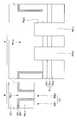
도 1은 본 발명의 실시예들에 따른 반도체소자의 평면도이고, 도 2 내지 도 8은 본 발명의 실시예들에 따른 반도체소자의 단면도들이다. 도 2 내지 도 8에 있어서, 참조부호 "A"로 표시된 부분은 도 1의 I-I′선을 따라 취해진 영역을 나타내고, 참조부호 "B"로 표시된 부분은 도 1의 II-II′선을 따라 취해진 영역을 나타낸다.1 is a plan view of a semiconductor device according to embodiments of the present invention, and FIGS. 2 to 8 are cross-sectional views of semiconductor devices according to embodiments of the present invention. In Figs. 2 to 8, the portion indicated by reference numeral "A" denotes an area taken along the line II 'of Fig. 1, and the portion denoted by reference numeral "B" is taken along the line II-II' of Fig. Represents an area.
우선, 도 1 및 도 8을 참조하여 본 발명의 실시예들에 따른 반도체소자를 설명하기로 한다.First, a semiconductor device according to example embodiments will be described with reference to FIGS. 1 and 8.
도 1 및 도 8을 참조하면, 반도체기판(100)에 활성영역(110a)을 한정하는 소자분리막(110s)이 제공된다. 여기서, 상기 소자분리막(110s)은 얕은 트렌치 소자분리막(shallow trench isolation)일 수 있다. 상기 활성영역(110a)은 장축 및 단축을 갖도록 제공되고, 장축 방향 및 단축 방향을 따라 2차원적으로 복수개가 배열될 수 있다. 상기 소자분리막(110s)과 상기 반도체기판(100) 사이에 절연성 라이 너(106)가 제공될 수 있다. 상기 절연성 라이너(106)는 실리콘 질화막과 같은 절연막으로 이루어질 수 있다. 상기 절연성 라이너(106)와 상기 반도체기판(100) 사이에 버퍼 산화막(104)이 제공될 수 있다. 상기 버퍼 산화막(104)은 실리콘 산화막과 같은 절연막으로 이루어질 수 있다.1 and 8, an
상기 활성영역(110a)을 가로지르는 상부 게이트 트렌치(120g)가 제공된다. 상기 상부 게이트 트렌치(120g)와 양쪽 끝이 중첩하며 상기 상부 게이트 트렌치(120g)보다 낮은 레벨에 위치하는 하부 게이트 트렌치(130g)가 제공된다. 여기서, 상기 하부 게이트 트렌치(130g)는 상기 상부 게이트 트렌치(120g)의 측벽과 이격되도록 상기 상부 게이트 트렌치(120g)보다 작은 폭을 갖는다.An
상기 상부 게이트 트렌치(120g)의 측벽과 상기 하부 게이트 트렌치(130g) 사이에 위치하는 상기 상부 게이트 트렌치(120g)의 바닥면을 부분적으로 덮으며 상기 하부 게이트 트렌치(130g)를 채우고, 상기 하부 게이트 트렌치(130g)의 바닥면 및 측벽에 인접하는 활성영역의 측벽을 덮는 게이트 패턴(140)이 제공된다. 여기서, 상기 게이트 패턴(140)은 상기 상부 게이트 트렌치(120g)의 측벽과 이격될 수 있다. 상기 게이트 패턴(140)은 차례로 적층된 게이트 유전막(134) 및 게이트 전극(136)으로 형성될 수 있다. 상기 게이트 유전막(134)은 실리콘 산화막 또는 고유전막(high-k dielectric layer)으로 이루어질 수 있다. 상기 게이트 전극(136)은 폴리 실리콘막, 금속막 및 실리사이드막으로 이루어진 군으로부터 선택된 적어도 하나의 막을 포함할 수 있다. 상기 게이트 패턴(140)에 의해 덮인 상기 하부 게이트 트렌치(130g)의 바닥면에 인접하는 상기 활성영역(110a) 측벽의 상하폭(W1)은 상기 게이트 패턴(140)에 의해 덮인 상기 하부 게이트 트렌치(130g)의 측벽에 인접하는 상기 활성영역(110a) 측벽의 좌우폭(W2)과 같거나 클 수 있다.Partially fills the
상기 상부 게이트 트렌치(120g)의 측벽과 상기 게이트 패턴(140) 사이에 개재된 절연성 스페이서(145)가 제공될 수 있다. 상기 절연성 스페이서(145)는 실리콘 질화막 또는 실리콘 산화막과 같은 절연막으로 이루어질 수 있다.An insulating
상기 상부 게이트 트렌치(120g)에 인접하는 활성영역(110a)에 소스/드레인 영역들(150)이 제공될 수 있다. 보다 바람직하게는 상기 소스/드레인 영역들(150)은 상기 절연성 스페이서(145)의 측벽 및 바닥면에 인접하는 활성영역에 제공될 수 있다. 따라서, 상기 소스/드레인 영역들(150)과 상기 게이트 패턴(140)의 중첩면적을 최소화될 수 있다. 그 결과, 상기 소스/드레인 영역들(150)과 상기 게이트 패턴(140) 사이의 중첩면적이 최소화됨에 따라, GIDL(gate induced drain leakage)을 최소화할 수 있다.Source /
상기 게이트 패턴(140)이 상기 하부 게이트 트렌치(130g)를 채움으로써, 상기 소스/드레인 영역들(150) 사이에 리세스 채널이 형성될 수 있다. 또한, 상기 게이트 패턴(140)이 상기 하부 게이트 트렌치(130g)의 바닥면 및 측벽에 인접하는 활성영역(110a)의 측벽을 덮음으로 인하여 핀 구조가 형성될 수 있다. 따라서, 리세스 채널 구조 및 핀 구조를 갖는 트랜지스터가 제공될 수 있다.As the
상술한 바와 같이, 상기 소스/드레인 영역들(150) 사이에 리세스 채널이 형성되므로, 트랜지스터의 유효 채널 길이(effective channel length)를 증가시킬 수 있다. 그 결과, 단채널 효과(short channel effect)를 억제할 수 있다. 더 나아가, 반도체소자의 고접적화를 구현할 수 있다.As described above, since a recess channel is formed between the source /
또한, 상기 게이트 패턴(140)이 상기 하부 게이트 트렌치(130g)의 바닥면 및 측벽에 인접하는 활성영역(110a)의 측벽을 덮음과 아울러 상기 상부 게이트 트렌치(120g)의 바닥면을 부분적으로 덮음으로 인하여, 상기 게이트 전극(140)의 채널에 대한 제어 능력(controllability)을 향상시킬 수 있다. 이에 따라, 리세스 채널을 가짐에도 불구하고 트랜지스터의 온-전류 특성을 향상시키고, 바디 효과를 억제할 수 있다. 따라서, 트랜지스터의 동작속도를 증가시킬 수 있다.In addition, the
더 나아가, 상기 소스/드레인 영역들(150)이 상기 상부 게이트 트렌치(120g)에 인접하는 활성영역, 보다 구체적으로 상기 절연성 스페이서(145)의 측벽 및 바닥면에 인접하는 활성영역에 제공됨으로 인하여 상기 소스/드레인 영역들(150)과 상기 게이트 전극(136) 사이의 중첩 면적을 최소화할 수 있다. 이에 따라, 상기 게이트 전극(136)과 상기 소스/드레인 영역들(150) 사이의 전기장(electric field)을 최소화시킬 수 있다. 그 결과, 트래지스터의 GIDL(Gate induced drain leakage)을 억제할 수 있다. 따라서, 저전력에서 동작하면서 동작속도가 빠른 트랜지스터를 제공할 수 있다.Furthermore, the source /
상기 소스/드레인 영역들(150) 중 선택된 하나에 전기적으로 접속된 정보 저장 요소(data storage element; 190)가 제공될 수 있다. 상기 정보 저장 요소(190)는 스토리지 커패시터(storage capacitor)일 수 있다. 상기 소스/드레인 영역들(150) 중 선택된 하나의 영역과 상기 정보 저장 요소(190) 사이에 베리드 콘택 플러그(185)가 제공될 수 있다. 또한, 상기 소스/드레인 영역들(150) 중 선택된 하 나의 영역과 상기 베리드 콘택 플러그(185) 사이에 제1 랜딩 패드(155s)가 제공될 수 있다. 더 나아가, 상기 소스/드레인 영역들(150) 중 상기 정보 저장 요소(190)와 전기적으로 접속되지 않은 영역은 도전성 라인(170)과 전기적으로 접속될 수 있다. 상기 도전성 라인(170)은 비트라인으로 정의되고, 상기 게이트 전극(136)은 워드라인으로 정의될 수 있다. 상기 도전성 라인(170)과 상기 소스/드레인 영역들(150)중 선택된 영역 사이에는 다이렉트 콘택 플러그(165)가 개재될 수 있다. 또한, 상기 다이렉트 콘택 플러그(165)와 상기 소스/드레인 영역들(150)중 선택된 영역 사이에는 제2 랜딩 패드(155b)가 개재될 수 있다.A
상술한 바와 같이 리세스 채널 구조 및 핀 구조를 갖는 트랜지스터를 셀 트랜지스터로 채택하는 디램과 같은 메모리 소자를 제공할 수 있다. 따라서, 정보 보유(data retention) 특성이 향상된 디램과 같은 메모리 소자를 제공할 수 있다. 이와 같이 제공된 디램과 같은 메모리 소자를 채택하는 전자제품들을 제공할 수 있다 따라서, 저전력 및 고성능의 전자제품을 제공할 수 있다.As described above, a memory device such as a DRAM employing a transistor having a recess channel structure and a fin structure as a cell transistor can be provided. Therefore, a memory device such as a DRAM having improved data retention characteristics can be provided. It is possible to provide electronic products employing a memory device such as a DRAM provided as described above, and thus it is possible to provide low power and high performance electronic products.
다음으로, 도 1 내지 도 8을 참조하여 본 발명의 실시예들에 따른 반도체소자의 제조방법을 설명하기로 한다.Next, a method of manufacturing a semiconductor device according to embodiments of the present invention will be described with reference to FIGS. 1 to 8.
도 1 및 도 2를 참조하면, 반도체기판(100)에 활성영역(110a)을 한정하는 소자분리막(110s)을 형성한다. 한편, 상기 소자분리막(110s)에 의해 복수개의 활성영역들(110a)이 한정될 수 있다. 상기 소자분리막(110s)에 의해 복수개의 활성영역들(110a)이 한정되는 경우에, 상기 활성영역들(110a)의 각각은 장축 및 단축을 가 지며, 상기 활성영역들(110a)은 장축 방향 및 단축 방향을 따라 2차원적으로 배열될 수 있다.1 and 2, an
상기 소자분리막(110s)은 얕은 트렌치 소자분리 기술(shallow trench isolation technique)을 이용하여 형성할 수 있다. 구체적으로, 상기 소자분리막(110s)을 형성하는 것은 상기 반도체 기판(100)의 소정영역을 식각하여 소자분리 트렌치를 형성하고, 상기 소자분리 트렌치를 채우는 절연막을 형성하는 것을 포함할 수 있다. 한편, 상기 반도체 기판(100)을 식각하여 상기 소자분리 트렌치를 형성한 후에, 상기 트렌치의 내벽에 버퍼 산화막(104) 및 절연성 라이너(106)를 차례로 형성할 수 있다.상기 버퍼 산화막(104)을 형성하는 이유는 상기 소자분리 트렌치를 형성하는 동안에 상기 반도체기판(100)에 가해진 식각 손상을 치유(curing)하기 위함이다. 상기 버퍼 산화막(104)은 상기 소자분리 트렌치를 갖는 기판을 열산화시킴으로써 형성될 수 있다. 상기 절연성 라이너(106)는 화학 기상 증착법에 의한 실리콘 질화막으로 형성할 수 있다. 상기 절연성 라이너(106)를 형성하는 이유는 반도체소자를 형성하기 위한 후속의 열공정들에 의하여 상기 소자분리 트렌치 내벽의 반도체기판이 후속의 열공정에 의하여 산화되는 것을 방지하기 위함이다. 또한, 상기 절연성 라이너(106)를 형성함으로써, 상기 활성영역(110a)의 평면적이 후속의 열공정에 의한 산화에 의하여 줄어드는 것을 억제할 수 있다.The
도 1 및 도 3을 참조하면, 상기 소자분리막(110s)을 갖는 기판 상에 상기 활성영역(110a)을 가로지르며 상기 소자분리막(110s)으로 연장된 개구부(115a)를 갖는 마스크(115)를 형성할 수 있다. 상기 마스크(115)는 차례로 적층된 하부 하드 마스크(112), 상부 하드 마스크(113) 및 희생 마스크로 형성될 수 있다. 상기 하부 하드 마스크(112)는 상기 소자분리막(110s) 및 상기 활성영역(110a)에 대해 식각선택비를 갖는 물질로 형성할 수 있다. 상기 상부 하드 마스크(113)는 상기 하부 하드 마스크(112) 및 상기 소자분리막(110s)에 대해 식각선택비를 갖는 물질로 형성할 수 있다. 예를 들어, 상기 하부 하드 마스크(112)가 실리콘 질화막으로 형성되는 경우에, 상기 상부 하드 마스크(113)는 실리콘막 또는 비정질 탄소막으로 형성할 수 있다. 상기 희생 마스크(115)는 포토레지스트막으로 형성될 수 있다. 1 and 3, a
한편, 상기 마스크(115)의 상기 개구부(115a)는 포켓 구조(pocket structure)로 형성될 수 있다. 구체적으로, 상기 활성영역(110a)이 복수개가 제공되는 경우에, 상기 활성영역들(110a)의 장축 방향을 따라 배열된 활성영역들(110a) 사이에 위치하는 소자분리막이 상기 마스크(115)에 의해 덮일 수 있도록 상기 개구부(115a)는 상기 활성영역들(110a)을 가로지르며 상기 소자분리막(110s)으로 연장되는 포켓 구조로 형성될 수 있다. 즉, 도 3에 도시된 바와 같이 상기 활성영역들(110a)의 단축에 실질적으로 평행한 상기 활성영역들(110a)의 측벽들 사이에 위치하는 소자분리막(110s)은 상기 마스크(115)에 의해 덮일 수 있다.Meanwhile, the
한편, 도면에 도시하지 않았지만 상기 하부 하드 마스크(112)를 형성하기 전에, 패드 산화막을 형성할 수 있다. 상기 하부 하드 마스크(112)가 실리콘 질화막으로 형성되는 경우에, 상기 패드 산화막은 상기 활성영역(110a)과 상기 하부 하드 마스크(112) 사이의 열팽창계수(thermal expansion coefficient)의 차이에 기인하는 스트레스를 완화시킬 수 있다.Although not shown in the drawings, before the lower
상기 마스크(115)를 식각마스크로 하여 상기 개구부(115a)에 의해 노출된 상기 활성영역(110a)을 식각할 수 있다. 상기 마스크(115)를 식각마스크로 하여 상기 활성영역(110a)을 식각하는 것은 이방성 식각 공정을 이용하여 수행할 수 있다. 그 결과, 상기 활성영역(110a)을 가로지르는 상부 게이트 트렌치(120g)가 형성될 수 있다.The
상기 마스크(115)를 식각마스크로 이용하여 상기 개구부(115a)에 의해 노출된 상기 소자분리막(110s)을 식각할 수 있다. 그 결과, 상기 활성영역(110a)을 가로지르는 상부 게이트 트렌치(120g) 및 상기 상부 게이트 트렌치(120g)로부터 상기 소자분리막(110s)으로 연장된 상부 필드 트렌치(120f)로 이루어진 상부 트렌치(121)가 형성될 수 있다.The
도 1 및 도 4를 참조하면, 상기 희생 마스크(114)를 제거할 수 있다. 상기 하부 하드 마스크(112), 상기 상부 하드 마스크(114) 및 상기 상부 트렌치(121)의 측벽들을 덮는 희생 스페이서(125)를 형성할 수 있다. 그 결과, 상기 상부 트렌치(121)의 바닥면이 부분적으로 노출될 수 있다. 즉, 상기 상부 게이트 트렌치(120g) 및 상기 상부 필드 트렌치(120f)의 바닥면들이 부분적으로 노출될 수 있다. 상기 희생 스페이서(125)는 상기 하부 하드 마스크(112)와 동일한 식각율을 갖는 물질로 형성될 수 있다. 예를 들면, 상기 하부 하드 마스크(112)가 실리콘 질화막으로 형성되는 경우에, 상기 희생 스페이서(125)도 실리콘 질화막으로 형성할 수 있다.1 and 4, the
도 1 및 도 5를 참조하면, 상기 희생 스페이서(125) 및 상기 상부 하드 마스 크(113)를 식각마스크로 하여 상기 상부 게이트 트렌치(120g)의 바닥면을 식각하여 하부 게이트 트렌치(130g)를 형성할 수 있다. 여기서, 상기 상부 게이트 트렌치(120g)의 바닥면을 식각하는 것을 이방성 식각 공정을 이용할 수 있다. 따라서, 상기 하부 게이트 트렌치(130g)는 상기 상부 게이트 트렌치(120g)보다 작은 폭을 갖는다. 또한, 상기 하부 게이트 트렌치(130g)의 양쪽 끝은 상기 상부 게이트 트렌치(120g)의 양쪽 끝과 중첩할 수 있다. 따라서, 상기 하부 게이트 트렌치(130g)에 의해 상기 소자분리막(110s)의 소정영역이 노출될 수 있다.1 and 5, the bottom surface of the
한편, 상기 상부 하드 마스크(113)가 실리콘막으로 형성되고, 상기 활성영역(110a)이 단결정 실리콘으로 이루어진 경우에, 상기 하부 게이트 트렌치(130g)를 형성하는 동안에 상기 상부 하드 마스크(113)가 식각되어 제거될 수 있다. 따라서, 상기 하부 하드 마스크(112) 및 상기 희생 스페이서(125)가 잔존할 수 있다. 이와 같이, 상기 상부 하드 마스크(113)가 상기 활성영역(110a)과 동일한 물질로 형성하는 경우에, 상기 상부 하드 마스크(113)를 제거하기 위한 별도의 식각공정을 생략할 수 있으므로 반도체소자의 제조 비용을 감소시킴과 아울러 공정 시간을 감축할 수 있다. 이와는 달리, 상기 상부 하드 마스크(113)가 비정질 탄소막과 같은 물질로 형성하는 경우에, 상기 상부 하드 마스크(113)를 제거하기 위한 식각 공정을 진행할 수 있다.Meanwhile, when the upper
상기 하부 하드 마스크(112) 및 상기 희생 스페이서(125)를 식각마스크로 이용하여 상기 하부 게이트 트렌치(130g)에 의해 노출된 소자분리막(110s)을 부분 식각하여 상기 하부 게이트 트렌치(130g)의 바닥면 및 측벽에 인접하는 활성영 역(110a)의 측벽을 노출시키는 하부 필드 트렌치(130f)를 형성할 수 있다. 여기서, 상기 하부 게이트 트렌치(130g)에 의해 노출된 상기 소자분리막(110s)을 부분식각하는 것은 상기 소자분리막(110s)에 대해 높은 식각율을 갖는 등방성 식각 공정을 이용할 수 있다. 따라서, 상기 하부 게이트 트렌치(130g)의 바닥면에 인접하는 상기 노출된 활성영역(110a) 측벽의 상하폭(W1)은 상기 하부 게이트 트렌치(130g)의 측벽에 인접하는 상기 노출된 활성영역(110a) 측벽의 좌우폭(W2)과 같을 수 있다.The bottom surface of the
한편, 상기 하부 하드 마스크(112) 및 상기 희생 스페이서(125)를 식각마스크로 하여 상기 상부 필드 트렌치(120f)의 바닥면을 이방성 식각하여 예비 하부 필드 트렌치를 형성하고, 상기 예비 하부 필드 트렌치 측벽 및 바닥면의 소자분리막을 등방성 식각하여 상기 하부 게이트 트렌치(130g)의 바닥면 및 측벽에 인접하는 활성영역의 측벽을 노출시키는 하부 필드 트렌치(130f)를 형성할 수 있다. 그 결과, 상기 하부 게이트 트렌치(130a) 및 상기 하부 필드 트렌치(130f)로 이루어진 하부 트렌치(131)가 형성될 수 있다. 한편, 후속 공정에 의해 완성되는 트랜지스터의 온 전류 특성을 더욱 향상시키기 위하여 상기 예비 하부 필드 트렌치가 상기 하부 게이트 트렌치(130f)보다 낮은 바닥면을 갖도록 형성할 수 있다. 따라서, 상기 하부 필드 트렌치(130f)는 상기 하부 게이트 트렌치(130g)의 측벽 및 바닥면에 인접하는 활성영역(110a)의 측벽을 노출시킬 수 있다. 여기서, 상기 하부 게이트 트렌치(130g)의 바닥면에 인접하는 상기 노출된 활성영역(110a) 측벽의 상하폭(W1)은 상기 하부 게이트 트렌치(130g)의 측벽에 인접하는 상기 노출된 활성영역(110a) 측벽의 좌우폭(W2)보다 클 수 있다. 이러한 것은 후속 공정에 의해 형성되는 게이트 패턴과 상기 활성영역(110a)의 측벽의 중첩면적을 증가시킴으로써 트랜지스터의 온 전류 특성을 향상시킬 수 있다. 즉, 트랜지스터의 동작속도를 향상시킬 수 있다.Meanwhile, the bottom surface of the
따라서, 상기 하부 게이트 트렌치(130g)의 바닥면에 인접하는 상기 노출된 활성영역(110a) 측벽의 상하폭(W1)은 상기 하부 게이트 트렌치(130g)의 측벽에 인접하는 상기 노출된 활성영역(110a) 측벽의 좌우폭(W2)과 같거나 클 수 있다.Accordingly, the upper and lower widths W1 of the sidewalls of the exposed
이어서, 상기 하부 하드 마스크(112) 및 상기 희생 스페이서(125)를 제거하여 도 6에 도시된 바와 같이 상기 상부 게이트 트렌치(120g)의 측벽 및 바닥면을 노출시킬 수 있다.Subsequently, the lower
도 1 및 도 7을 참조하면, 상기 하부 트렌치(131)를 채우며 상기 상부 게이트 트렌치(120g)의 측벽과 이격되도록 상기 상부 게이트 트렌치(120g)의 바닥면을 부분적으로 덮는 게이트 패턴(140)을 형성한다. 상기 게이트 패턴(140)은 상기 하부 게이트 트렌치(130g) 및 상기 하부 필드 트렌치(130g)를 채우도록 형성되므로, 상기 하부 필드 트렌치(130g)에 의해 노출된 상기 활성영역(110a)의 측벽을 덮을 수 있다. 도 7에서, 지시부호 "FG"는 상기 게이트 패턴(140)에 의해 덮인 상기 활성영역(110a)의 측벽을 나타낸다. 따라서, 상기 게이트 패턴(140)에 의해 덮인 상기 활성영역(110a)의 측벽(FG)은 상기 하부 필드 트렌치(130f)에 의해 노출된 활성영역의 측벽에 대응할 수 있다.1 and 7, a
상기 게이트 패턴(140)을 형성하는 것은 상기 하부 하드 마스크(112) 및 상기 희생 스페이서(125)를 제거하여 상기 상부 게이트 트렌치(120g)의 측벽 및 바닥면을 노출시킨 기판 상에 게이트 막을 형성하고, 상기 게이트 막을 패터닝하는 것 을 포함할 수 있다. 상기 게이트 패턴(140)은 차례로 적층된 게이트 유전막(134) 및 게이트 전극(136)으로 형성할 수 있다. 상기 게이트 유전막(134)은 실리콘 산화막 또는 고유전막(high-k dielectric layer)으로 형성할 수 있다. 상기 게이트 전극(136)은 폴리 실리콘막, 금속막 및 실리사이드막으로 이루어진 군으로부터 선택된 적어도 하나의 막을 포함하도록 형성할 수 있다. 한편, 상기 게이트 막을 패터닝하기 전에, 하드 마스크로 이용하는 캐핑막(143)을 형성할 수 있다. 상기 캐핑막(143)은 실리콘 질화막으로 형성할 수 있다.The
상기 상부 게이트 트렌치(120g)의 측벽과 상기 게이트 패턴(140) 사이를 채우는 절연성 스페이서(145)를 형성할 수 있다. 상기 절연성 스페이서(145)를 형성하는 것은 상기 게이트 패턴(140)을 갖는 기판 상에 스페이서 절연막을 형성하고, 상기 스페이서 절연막을 이방성식각 하는 것을 포함할 수 있다.An insulating
상기 게이트 패턴(140) 양 옆의 활성영역(110a)에 소스/드레인 영역들(150)을 형성할 수 있다. 보다 바람직하게는 상기 절연성 스페이서(145)의 측벽 및 바닥면에 인접하는 활성영역에 소스/드레인 영역들(150)을 형성할 수 있다.Source /
상기 소스/드레인 영역들(150)을 형성하는 것은 상기 게이트 패턴(140)과의 중첩면적을 최소화하도록 상기 상부 게이트 트렌치(120g)의 측벽에 인접하는 활성영역에 불순물 이온들을 주입하고, 상기 불순물 이온들을 상기 절연성 스페이서(145) 하부에 인접하는 활성영역으로 확산시키는 것을 포함할 수 있다. 여기서, 상부 게이트 트렌치(120g)의 측벽에 인접하는 활성영역에 불순물 이온들을 주입하는 것은 상기 소자분리막(110s), 상기 게이트 패턴(140) 및 상기 절연성 스페이 서(145)를 이온주입마스크로 하여 상기 활성영역(110a)에 불순물 이온들을 주입하는 것을 포함할 수 있다. 따라서, 상기 소스/드레인 영역들(150)과 상기 게이트 패턴(140) 사이의 중첩면적을 최소화할 수 있다. 그 결과, 상기 소스/드레인 영역들(150)과 상기 게이트 전극(136) 사이의 중첩면적을 최소화할 수 있다.Forming the source /
상술한 바와 같은 구성요소들로부터 리세스 채널 구조 및 핀 구조를 갖는 트랜지스터가 제공될 수 있다. 다시 말하면, 상기 게이트 패턴(140)이 상기 하부 게이트 트렌치(130g)를 채움으로 인하여 상기 소스/드레인 영역들(150) 사이에 리세스 채널이 형성될 수 있다. 또한, 상기 게이트 패턴(140)이 상기 하부 게이트 트렌치(130g)의 바닥면 및 측벽에 인접하는 활성영역의 측벽을 덮음과 아울러 상기 하부 게이트 트렌치(130g)에 인접한 상기 상부 게이트 트렌치(120g)의 바닥면을 부분적으로 덮으므로 인하여 핀 구조가 형성될 수 있다. 이러한 리세스 채널 구조 및 핀 구조를 갖는 트랜지스터에 대해 앞에서 설명한 바 있으므로 자세한 설명은 생략하기로 한다.Transistors having a recess channel structure and a fin structure may be provided from the above components. In other words, a recess channel may be formed between the source /
도 1 및 도 8을 참조하면, 자기정렬 콘택 공정(self-align contact process)을 이용하여 상기 소스/드레인 영역들(150)에 전기적으로 접속하는 제1 랜딩 패드(155s) 및 제2 랜딩 패드(155b)를 형성할 수 있다. 상기 제1 랜딩 패드(155s)는 상기 소스/드레인 영역들(150) 중 선택된 하나에 전기적으로 접속될 수 있다.1 and 8, the first and
상기 랜딩 패드들(155s, 155b)을 갖는 기판 상에 하부 절연막(160)을 형성할 수 있다. 상기 하부 절연막(160)을 관통하며 상기 제2 랜딩 패드(155b)에 전기적으로 접속하는 다이렉트 콘택 플러그(165)를 형성할 수 있다. 상기 하부 절연막(160) 상에 상기 다이렉트 콘택 플러그(165)를 덮는 도전성 라인(170)을 형성할 수 있다. 상기 도전성 라인(170)은 비트라인으로 정의할 수 있다. 상기 도전성 라인(170)을 비트라인으로 정의하는 경우에, 상기 게이트 전극(136)은 워드라인으로 정의할 수 있다. 상기 도전성 라인(170)을 갖는 기판 상에 상부 절연막(175)을 형성할 수 있다. 상기 상부 절연막(175) 및 상기 하부 절연막(160)은 실리콘 산화막으로 형성할 수 있다. 상기 상부 절연막(175) 및 상기 하부 절연막(160)을 차례로 관통하며 상기 제1 랜딩 패드(155s)와 전기적으로 접속하는 베리드 콘택 플러그(180)를 형성할 수 있다. 상기 상부 절연막(175) 상에 상기 베리드 콘택 플러그(185)를 덮는 정보 저장 요소(data storage element; 190)를 형성할 수 있다. 상기 정보 저장 요소(190)는 스토리지 커패시터(storage capacitor)일 수 있다. 따라서, 리세스 채널 구조 및 핀 구조를 갖는 트랜지스터를 셀 트랜지스터로 채택하는 디램과 같은 메모리 소자를 제공할 수 있다.The lower
상술한 바와 같이 본 발명에 따르면, 소스/드레인 영역들과 게이트 전극 사이의 중첩면적을 최소화하면서 리세스 채널 구조 및 핀 구조를 갖는 트랜지스터를 제공한다. 소스/드레인 영역들과 게이트 전극 사이의 중첩면적을 최소화할 수 있으므로, 트래지스터의 GIDL(Gate induced drain leakage)을 억제할 수 있다. 또한, 리세스 채널 구조 및 핀 구조를 가짐으로, 단채널 효과(short channel effect)를 억제함과 아울러 트랜지스터의 온 전류 특성을 향상시킬 수 있다. 또한, 이와 같은 트랜지스터를 셀 트랜지스터로 채택하는 디램과 같은 메모리 소자의 정보 보 유(data retention) 특성을 향상시킬 수 있다.According to the present invention as described above, there is provided a transistor having a recess channel structure and a fin structure while minimizing the overlapping area between the source / drain regions and the gate electrode. Since the overlap area between the source / drain regions and the gate electrode can be minimized, gate induced drain leakage (GIDL) of the transistor can be suppressed. In addition, by having a recess channel structure and a fin structure, it is possible to suppress short channel effects and to improve on current characteristics of the transistor. In addition, data retention characteristics of memory devices such as DRAMs employing such transistors as cell transistors may be improved.
Claims (26)
Translated fromKoreanPriority Applications (3)
| Application Number | Priority Date | Filing Date | Title |
|---|---|---|---|
| KR1020060076303AKR100827656B1 (en) | 2006-08-11 | 2006-08-11 | Transistor having recess channel structure and fin structure, semiconductor device adopting same and manufacturing method thereof |
| US11/696,541US20080035991A1 (en) | 2006-08-11 | 2007-04-04 | Transistor Having Recess Channel Structure and Fin Structure, Semiconductor Device Employing the Transistor, and Method of Fabricating the Semiconductor Device |
| JP2007210320AJP2008047909A (en) | 2006-08-11 | 2007-08-10 | Transistor having recess channel structure and fin structure, semiconductor device employing the same, and manufacturing method thereof |
Applications Claiming Priority (1)
| Application Number | Priority Date | Filing Date | Title |
|---|---|---|---|
| KR1020060076303AKR100827656B1 (en) | 2006-08-11 | 2006-08-11 | Transistor having recess channel structure and fin structure, semiconductor device adopting same and manufacturing method thereof |
Publications (2)
| Publication Number | Publication Date |
|---|---|
| KR20080014503A KR20080014503A (en) | 2008-02-14 |
| KR100827656B1true KR100827656B1 (en) | 2008-05-07 |
Family
ID=39049854
Family Applications (1)
| Application Number | Title | Priority Date | Filing Date |
|---|---|---|---|
| KR1020060076303AExpired - Fee RelatedKR100827656B1 (en) | 2006-08-11 | 2006-08-11 | Transistor having recess channel structure and fin structure, semiconductor device adopting same and manufacturing method thereof |
Country Status (3)
| Country | Link |
|---|---|
| US (1) | US20080035991A1 (en) |
| JP (1) | JP2008047909A (en) |
| KR (1) | KR100827656B1 (en) |
Cited By (2)
| Publication number | Priority date | Publication date | Assignee | Title |
|---|---|---|---|---|
| KR101205037B1 (en)* | 2011-02-28 | 2012-11-26 | 에스케이하이닉스 주식회사 | Semiconductor device and method for fabricating the same |
| KR101438291B1 (en)* | 2012-10-26 | 2014-09-04 | 타이완 세미콘덕터 매뉴팩쳐링 컴퍼니 리미티드 | Finfet with dummy gate on non-recessed shallow trench isolation(sti) |
Families Citing this family (22)
| Publication number | Priority date | Publication date | Assignee | Title |
|---|---|---|---|---|
| JP2009182114A (en)* | 2008-01-30 | 2009-08-13 | Elpida Memory Inc | Semiconductor device and manufacturing method thereof |
| JP5557442B2 (en)* | 2008-10-31 | 2014-07-23 | ピーエスフォー ルクスコ エスエイアールエル | Semiconductor device |
| KR101205173B1 (en) | 2009-07-28 | 2012-11-27 | 에스케이하이닉스 주식회사 | Method for forming semiconductor device |
| JP2011054629A (en) | 2009-08-31 | 2011-03-17 | Elpida Memory Inc | Semiconductor device and manufacturing method thereof |
| US20110140232A1 (en)* | 2009-12-15 | 2011-06-16 | Intersil Americas Inc. | Methods of forming a thermal conduction region in a semiconductor structure and structures resulting therefrom |
| JP5450480B2 (en)* | 2011-03-03 | 2014-03-26 | 株式会社東芝 | Semiconductor device |
| JP2012204799A (en)* | 2011-03-28 | 2012-10-22 | Toshiba Corp | Semiconductor memory device and method of manufacturing the same |
| JP2012253122A (en)* | 2011-06-01 | 2012-12-20 | Elpida Memory Inc | Semiconductor device manufacturing method and data processing system |
| KR101858622B1 (en)* | 2011-07-01 | 2018-06-28 | 삼성전자주식회사 | Semiconductor device |
| US8395209B1 (en)* | 2011-09-22 | 2013-03-12 | Nanya Technology Corp. | Single-sided access device and fabrication method thereof |
| TWI462275B (en)* | 2011-11-14 | 2014-11-21 | Inotera Memories Inc | Memory structure |
| WO2014077209A1 (en)* | 2012-11-14 | 2014-05-22 | ピーエスフォー ルクスコ エスエイアールエル | Semiconductor device and method for manufacturing same |
| KR102291571B1 (en)* | 2015-01-13 | 2021-08-18 | 삼성전자주식회사 | Semiconductor device and the fabricating method thereof |
| KR102312346B1 (en)* | 2015-02-23 | 2021-10-14 | 삼성전자주식회사 | Methods of Fabricating Semiconductor Devices |
| KR102448597B1 (en)* | 2015-06-24 | 2022-09-27 | 삼성전자주식회사 | semiconductor device |
| KR102399027B1 (en)* | 2015-06-24 | 2022-05-16 | 삼성전자주식회사 | Semiconductor device |
| KR102379701B1 (en)* | 2015-10-19 | 2022-03-28 | 삼성전자주식회사 | Semiconductor device having multi-channel and method of forming the same |
| TWI750375B (en)* | 2018-05-16 | 2021-12-21 | 力智電子股份有限公司 | Trench gate mosfet and method of forming the same |
| CN110875183B (en)* | 2018-08-29 | 2023-04-21 | 中芯国际集成电路制造(上海)有限公司 | Semiconductor device and method of forming the same |
| US11195753B2 (en)* | 2018-09-18 | 2021-12-07 | International Business Machines Corporation | Tiered-profile contact for semiconductor |
| CN112038341B (en)* | 2019-06-04 | 2024-06-21 | 长鑫存储技术有限公司 | Memory structure and forming method thereof |
| CN112447584B (en)* | 2019-08-30 | 2024-10-18 | 长鑫存储技术有限公司 | Semiconductor structure and preparation method thereof, and storage device |
Citations (2)
| Publication number | Priority date | Publication date | Assignee | Title |
|---|---|---|---|---|
| KR20060065946A (en)* | 2004-12-11 | 2006-06-15 | 경북대학교 산학협력단 | Saddle-type OS element |
| KR100648635B1 (en)* | 2005-09-06 | 2006-11-23 | 경북대학교 산학협력단 | MOOS device with a saddle structure |
Family Cites Families (8)
| Publication number | Priority date | Publication date | Assignee | Title |
|---|---|---|---|---|
| US6413802B1 (en)* | 2000-10-23 | 2002-07-02 | The Regents Of The University Of California | Finfet transistor structures having a double gate channel extending vertically from a substrate and methods of manufacture |
| KR100558544B1 (en)* | 2003-07-23 | 2006-03-10 | 삼성전자주식회사 | Recess gate transistor structure and formation method accordingly |
| KR100500473B1 (en)* | 2003-10-22 | 2005-07-12 | 삼성전자주식회사 | Recess gate transistor structure for use in semiconductor device and method thereof |
| KR100513405B1 (en)* | 2003-12-16 | 2005-09-09 | 삼성전자주식회사 | Method for forming fin field effect transistor |
| KR100577562B1 (en)* | 2004-02-05 | 2006-05-08 | 삼성전자주식회사 | Fin transistor formation method and its structure |
| US7132333B2 (en)* | 2004-09-10 | 2006-11-07 | Infineon Technologies Ag | Transistor, memory cell array and method of manufacturing a transistor |
| KR100724575B1 (en)* | 2006-06-28 | 2007-06-04 | 삼성전자주식회사 | Semiconductor device having buried gate electrode and forming method thereof |
| US7612406B2 (en)* | 2006-09-08 | 2009-11-03 | Infineon Technologies Ag | Transistor, memory cell array and method of manufacturing a transistor |
- 2006
- 2006-08-11KRKR1020060076303Apatent/KR100827656B1/ennot_activeExpired - Fee Related
- 2007
- 2007-04-04USUS11/696,541patent/US20080035991A1/ennot_activeAbandoned
- 2007-08-10JPJP2007210320Apatent/JP2008047909A/enactivePending
Patent Citations (2)
| Publication number | Priority date | Publication date | Assignee | Title |
|---|---|---|---|---|
| KR20060065946A (en)* | 2004-12-11 | 2006-06-15 | 경북대학교 산학협력단 | Saddle-type OS element |
| KR100648635B1 (en)* | 2005-09-06 | 2006-11-23 | 경북대학교 산학협력단 | MOOS device with a saddle structure |
Cited By (4)
| Publication number | Priority date | Publication date | Assignee | Title |
|---|---|---|---|---|
| KR101205037B1 (en)* | 2011-02-28 | 2012-11-26 | 에스케이하이닉스 주식회사 | Semiconductor device and method for fabricating the same |
| KR101438291B1 (en)* | 2012-10-26 | 2014-09-04 | 타이완 세미콘덕터 매뉴팩쳐링 컴퍼니 리미티드 | Finfet with dummy gate on non-recessed shallow trench isolation(sti) |
| US9337318B2 (en) | 2012-10-26 | 2016-05-10 | Taiwan Semiconductor Manufacturing Company, Ltd. | FinFET with dummy gate on non-recessed shallow trench isolation (STI) |
| US9754842B2 (en) | 2012-10-26 | 2017-09-05 | Taiwan Semiconductor Manufacturing Company, Ltd. | FinFET with dummy gate on non-recessed shallow trench isolation (STI) |
Also Published As
| Publication number | Publication date |
|---|---|
| JP2008047909A (en) | 2008-02-28 |
| KR20080014503A (en) | 2008-02-14 |
| US20080035991A1 (en) | 2008-02-14 |
Similar Documents
| Publication | Publication Date | Title |
|---|---|---|
| KR100827656B1 (en) | Transistor having recess channel structure and fin structure, semiconductor device adopting same and manufacturing method thereof | |
| US7459358B2 (en) | Method for fabricating a semiconductor device | |
| US7718493B2 (en) | Method for forming semiconductor device | |
| KR100739653B1 (en) | Fin field effect transistor and its manufacturing method | |
| KR100843711B1 (en) | Semiconductor device adopting transistor having recess channel region and manufacturing method thereof | |
| US7675112B2 (en) | Semiconductor device with a surrounded channel transistor | |
| US7795670B2 (en) | Semiconductor device and method for fabricating the same | |
| US8373223B2 (en) | Semiconductor device and method for fabricating the same | |
| JP4552908B2 (en) | Manufacturing method of semiconductor device | |
| US7285456B2 (en) | Method of fabricating a fin field effect transistor having a plurality of protruding channels | |
| US8039327B2 (en) | Transistor forming methods | |
| US7563683B2 (en) | Transistor and method of fabricating the same | |
| US20090267133A1 (en) | Flash memory device and method for fabricating the same | |
| KR20050083305A (en) | Method for manufacturing fin field effect transistor | |
| KR100826981B1 (en) | Semiconductor element and manufacturing method thereof | |
| KR20080045451A (en) | Semiconductor device having MOS transistor with recess channel and method of manufacturing same | |
| KR101024777B1 (en) | Semiconductor device and manufacturing method thereof | |
| KR100979241B1 (en) | Semiconductor device and manufacturing method thereof | |
| KR100929629B1 (en) | Manufacturing Method of Semiconductor Device | |
| KR20090098282A (en) | Saddle Fin Transistor and Manufacturing Method Thereof | |
| KR20080065805A (en) | Manufacturing Method of Semiconductor Device | |
| KR20070002900A (en) | Manufacturing method of semiconductor device |
Legal Events
| Date | Code | Title | Description |
|---|---|---|---|
| A201 | Request for examination | ||
| PA0109 | Patent application | St.27 status event code:A-0-1-A10-A12-nap-PA0109 | |
| PA0201 | Request for examination | St.27 status event code:A-1-2-D10-D11-exm-PA0201 | |
| D13-X000 | Search requested | St.27 status event code:A-1-2-D10-D13-srh-X000 | |
| D14-X000 | Search report completed | St.27 status event code:A-1-2-D10-D14-srh-X000 | |
| E902 | Notification of reason for refusal | ||
| PE0902 | Notice of grounds for rejection | St.27 status event code:A-1-2-D10-D21-exm-PE0902 | |
| E13-X000 | Pre-grant limitation requested | St.27 status event code:A-2-3-E10-E13-lim-X000 | |
| P11-X000 | Amendment of application requested | St.27 status event code:A-2-2-P10-P11-nap-X000 | |
| P13-X000 | Application amended | St.27 status event code:A-2-2-P10-P13-nap-X000 | |
| E902 | Notification of reason for refusal | ||
| PE0902 | Notice of grounds for rejection | St.27 status event code:A-1-2-D10-D21-exm-PE0902 | |
| P11-X000 | Amendment of application requested | St.27 status event code:A-2-2-P10-P11-nap-X000 | |
| P13-X000 | Application amended | St.27 status event code:A-2-2-P10-P13-nap-X000 | |
| PG1501 | Laying open of application | St.27 status event code:A-1-1-Q10-Q12-nap-PG1501 | |
| E701 | Decision to grant or registration of patent right | ||
| PE0701 | Decision of registration | St.27 status event code:A-1-2-D10-D22-exm-PE0701 | |
| GRNT | Written decision to grant | ||
| PR0701 | Registration of establishment | St.27 status event code:A-2-4-F10-F11-exm-PR0701 | |
| PR1002 | Payment of registration fee | St.27 status event code:A-2-2-U10-U11-oth-PR1002 Fee payment year number:1 | |
| PG1601 | Publication of registration | St.27 status event code:A-4-4-Q10-Q13-nap-PG1601 | |
| PR1001 | Payment of annual fee | St.27 status event code:A-4-4-U10-U11-oth-PR1001 Fee payment year number:4 | |
| FPAY | Annual fee payment | ||
| PR1001 | Payment of annual fee | St.27 status event code:A-4-4-U10-U11-oth-PR1001 Fee payment year number:5 | |
| R18-X000 | Changes to party contact information recorded | St.27 status event code:A-5-5-R10-R18-oth-X000 | |
| FPAY | Annual fee payment | ||
| PR1001 | Payment of annual fee | St.27 status event code:A-4-4-U10-U11-oth-PR1001 Fee payment year number:6 | |
| PR1001 | Payment of annual fee | St.27 status event code:A-4-4-U10-U11-oth-PR1001 Fee payment year number:7 | |
| LAPS | Lapse due to unpaid annual fee | ||
| PC1903 | Unpaid annual fee | St.27 status event code:A-4-4-U10-U13-oth-PC1903 Not in force date:20150430 Payment event data comment text:Termination Category : DEFAULT_OF_REGISTRATION_FEE | |
| PC1903 | Unpaid annual fee | St.27 status event code:N-4-6-H10-H13-oth-PC1903 Ip right cessation event data comment text:Termination Category : DEFAULT_OF_REGISTRATION_FEE Not in force date:20150430 | |
| P22-X000 | Classification modified | St.27 status event code:A-4-4-P10-P22-nap-X000 |