KR100826692B1 - Semiconductor memory module with bus architecture - Google Patents
Semiconductor memory module with bus architectureDownload PDFInfo
- Publication number
- KR100826692B1 KR100826692B1KR1020060010511AKR20060010511AKR100826692B1KR 100826692 B1KR100826692 B1KR 100826692B1KR 1020060010511 AKR1020060010511 AKR 1020060010511AKR 20060010511 AKR20060010511 AKR 20060010511AKR 100826692 B1KR100826692 B1KR 100826692B1
- Authority
- KR
- South Korea
- Prior art keywords
- buses
- bus
- control
- module substrate
- memory
- Prior art date
- Legal status (The legal status is an assumption and is not a legal conclusion. Google has not performed a legal analysis and makes no representation as to the accuracy of the status listed.)
- Expired - Fee Related
Links
Images


Classifications
- G—PHYSICS
- G06—COMPUTING OR CALCULATING; COUNTING
- G06F—ELECTRIC DIGITAL DATA PROCESSING
- G06F13/00—Interconnection of, or transfer of information or other signals between, memories, input/output devices or central processing units
- G06F13/14—Handling requests for interconnection or transfer
- G—PHYSICS
- G11—INFORMATION STORAGE
- G11C—STATIC STORES
- G11C5/00—Details of stores covered by group G11C11/00
- G11C5/02—Disposition of storage elements, e.g. in the form of a matrix array
- G11C5/04—Supports for storage elements, e.g. memory modules; Mounting or fixing of storage elements on such supports
- G—PHYSICS
- G06—COMPUTING OR CALCULATING; COUNTING
- G06F—ELECTRIC DIGITAL DATA PROCESSING
- G06F13/00—Interconnection of, or transfer of information or other signals between, memories, input/output devices or central processing units
- G06F13/38—Information transfer, e.g. on bus
- G06F13/40—Bus structure
- G—PHYSICS
- G06—COMPUTING OR CALCULATING; COUNTING
- G06F—ELECTRIC DIGITAL DATA PROCESSING
- G06F3/00—Input arrangements for transferring data to be processed into a form capable of being handled by the computer; Output arrangements for transferring data from processing unit to output unit, e.g. interface arrangements
Landscapes
- Engineering & Computer Science (AREA)
- Theoretical Computer Science (AREA)
- General Engineering & Computer Science (AREA)
- Physics & Mathematics (AREA)
- General Physics & Mathematics (AREA)
- Human Computer Interaction (AREA)
- Computer Hardware Design (AREA)
- Dram (AREA)
Abstract
Translated fromKorean
Description
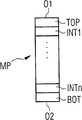
Translated fromKorean도 1a는 FBDIMM 메모리 모듈의 횡단면도,1A is a cross sectional view of an FBDIMM memory module,
도 1b는 FBDIMM 메모리 모듈의 모듈 기판의 횡단면도,1B is a cross sectional view of a module substrate of an FBDIMM memory module,
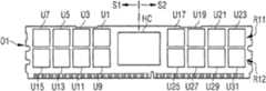
도 2a는 FBDIMM 메모리 모듈의 상면을 나타낸 도면,2A is a top view of an FBDIMM memory module;
도 2b는 FBDIMM 메모리 모듈의 하면을 나타낸 도면,FIG. 2B is a bottom view of the FBDIMM memory module; FIG.
도 3은 FBDIMM 메모리 모듈 상의 메모리 칩들의 메모리 셀 필드를 나타낸 도면,3 illustrates a memory cell field of memory chips on an FBDIMM memory module;
도 4는 본 발명에 따른 FBDIMM 메모리 모듈 상의 메모리 칩들을 제어하는 제어 소자를 나타낸 도면4 illustrates a control device for controlling memory chips on an FBDIMM memory module according to the present invention.
도 5는 선행 기술에 따른 CA 버스의 버스 구조를 갖는 FBDIMM 메모리 모듈의 하면을 본 발명에 따른 CA 버스 구조와 대비하여 나타낸 도면,FIG. 5 is a view illustrating a bottom surface of an FBDIMM memory module having a bus structure of a CA bus according to the prior art in comparison with a CA bus structure according to the present invention; FIG.
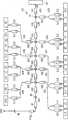
도 6은 선행 기술에 따른 CA 버스의 버스 구조를 나타낸 도면,6 illustrates a bus structure of a CA bus according to the prior art;
도 7은 본 발명에 따른 CA 버스의 버스 구조를 나타낸 도면,7 illustrates a bus structure of a CA bus according to the present invention;
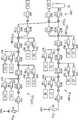
도 8a는 본 발명에 따른 ODTL 버스의 버스 구조를 나타낸 도면,8A illustrates a bus structure of an ODTL bus according to the present invention;
도 8b는 본 발명에 따른 다른 ODTL 버스의 버스 구조를 나타낸 도면,8B is a view showing a bus structure of another ODTL bus according to the present invention;
도 9는 본 발명에 따른 CLK 버스의 버스 구조를 나타낸 도면,9 illustrates a bus structure of a CLK bus according to the present invention;
도 10은 본 발명에 따른 CTRL 버스의 버스 구조를 나타낸 도면.10 illustrates a bus structure of a CTRL bus in accordance with the present invention.
도면의 주요 부분에 대한 부호의 설명Explanation of symbols for the main parts of the drawings
MP: 모듈 기판B: 반도체 메모리 소자들MP: Module Substrate B: Semiconductor Memory Devices
SB: 제어 소자U: 메모리 칩SB: control element U: memory chip
SZF: 메모리 셀 필드BL: 비트 라인SZF: memory cell field BL: bit line
WL: 워드 라인AT: 선택 트랜지스터WL: word line AT: select transistor
SC: 메모리 커패시터SZ: 메모리 셀SC: memory capacitor SZ: memory cell
ODTS: 활성화 신호DQ: 데이터 버스ODTS: Activation Signal DQ: Data Bus
HC: 허브 칩AS: 제어 회로HC: hub chip AS: control circuit
CAB: 커맨드 어드레스 버스CLKB: 클록 버스CAB: command address bus CLKB: clock bus
CTRLB: 제어 버스TB: 부분 버스CTRLB: control bus TB: partial bus
INT: 내부 층TOP: 상단 외층INT: inner layer TOP: upper outer layer
본 발명은 제어 회로가 제어 버스들, 클록 버스들, 및 어드레스 버스들을 경유하여 다수의 메모리 칩들을 제어하는 반도체 메모리 모듈에 관한 것이다.The present invention relates to a semiconductor memory module in which a control circuit controls a plurality of memory chips via control buses, clock buses, and address buses.
반도체 메모리 모듈, 예컨대 FBDIMM(풀리 버퍼드 듀얼-인라인 메모리 모듈 )(Fully Buffered Dual-In Line Memory Module)에서는, 메모리 제어기에 의해 직접 제어되는 것이 아니라 제어 소자, 예컨대 허브 칩을 경유하여 제어되는 다수의 반도체 메모리 소자들이 모듈 기판 상에 배치된다. 현재, 무엇보다도 특히 그 클록 주파수 및 그 비트율에 있어 상이한 4가지의 FBDIMM 모듈 카드들이 표준화되어 있다. 현재 표준화되어 있는 FBDIMM 카드에 속하는 것들로는, 비트율이 400 Mbit/s인 FBD400 카드, 비트율이 533 Mbit/s인 FBD533 카드, 비트율이 667 Mbit/s인 FBD667 카드, 및 비트율이 800 Mbit/s인 FBD800 카드가 있다.In semiconductor memory modules, such as Fully Buffered Dual-In Line Memory Modules (FBDIMMs), many of them are controlled via a control element, such as a hub chip, rather than directly controlled by a memory controller. Semiconductor memory devices are disposed on a module substrate. Currently, four different FBDIMM module cards, among other things in terms of their clock frequency and their bit rate, are standardized. Among the currently standardized FBDIMM cards are FBD400 cards with a bit rate of 400 Mbit / s, FBD533 cards with a bit rate of 533 Mbit / s, FBD667 cards with a bit rate of 667 Mbit / s, and 800 Mbit / s with a bit rate of There is an FBD800 card.
2R×4의 설계 구성에서는, FBDIMM 모듈 상의 "랭크(rank)"당 18개의 메모리 칩들이 있게 된다. 그러한 메모리 칩들은 모듈 기판 상의 반도체 메모리 소자들에 스택 배열(스택 DRAM 디바이스)로 배치된다. 2×스택(듀얼 스택) 설계에서는, 반도체 메모리 소자 내에 2개의 메모리 칩들이 스택 배열로 배치된다. 개개의 메모리 칩들은 정보를 저장하거나 저장된 정보를 판독하는 허브 칩 상의 제어 회로에 의해 제어 버스, 어드레스 버스, 및 클록 버스를 경유하여 제어된다. 2R×4 구성의 FBDIMM 메모리 모듈에서는, 허브 칩의 제어 회로가 4개의 클록 신호들을 제공하는데, 그 중에서 2개의 클록 신호들은 허브 칩의 좌측에 배치된 메모리 칩들을 급전하는데 사용되고, 다른 2개의 클록 신호들은 허브 칩의 우측에 배치된 메모리 칩들을 제어하는데 사용된다. 2R×4 구성의 FBDIMM 메모리 모듈 상에 존재하는 총 36개의 메모리 칩들에서는, 2개씩의 메모리 칩들을 구비한 9개의 반도체 메모리 소자들이 허브 칩의 좌측에 배치되고, 2개씩의 메모리 칩들을 구비한 9개의 반도체 메모리 소자들이 허브 칩의 우측에 배치된다. 즉, 허브 칩의 양측으로 총 18개의 메모리 칩들이 허브 칩의 제어 회로에 의해 제어되어야 한다.In a 2R × 4 design configuration, there are 18 memory chips per “rank” on the FBDIMM module. Such memory chips are disposed in a stack arrangement (stack DRAM device) on semiconductor memory elements on a module substrate. In a 2x stack (dual stack) design, two memory chips are arranged in a stack arrangement within a semiconductor memory device. Individual memory chips are controlled via a control bus, an address bus, and a clock bus by control circuitry on the hub chip that stores information or reads stored information. In a 2Bx4 FBDIMM memory module, the control circuit of the hub chip provides four clock signals, of which two clock signals are used to feed the memory chips disposed on the left side of the hub chip, and the other two clock signals. Are used to control memory chips disposed on the right side of the hub chip. In a total of 36 memory chips present on a 2B × 4 FBDIMM memory module, nine semiconductor memory elements with two memory chips are arranged on the left side of the hub chip, and nine with two memory chips. Semiconductor memory devices are disposed on the right side of the hub chip. That is, a total of 18 memory chips on both sides of the hub chip must be controlled by the control circuit of the hub chip.
메모리 칩들의 제어를 위해, 허브 칩은 4개의 클록 신호들을 제공하는데, 그 중에서 2개의 클록 신호들은 허브 칩의 좌측에 있는 메모리 칩들에 사용되고, 다른 2개의 클록 신호들은 허브 칩의 우측에 있는 메모리 칩들에 사용된다. 그를 위해, 허브 칩은 허브 칩의 좌측에 있는 2개의 클록 버스들 및 우측에 있는 2개의 클록 버스들을 제어한다. JEDEC 표준에 따르면, 허브 칩의 좌측과 우측에 있는 제1 클록 버스에는 10개씩의 메모리 칩들이 접속되고, 허브 칩의 좌측과 우측에 있는 제2 클록 버스에는 8개씩의 메모리 칩들이 접속된다. 즉, 클록 버스들은 10/8/10/8의 구성을 갖는다.For control of the memory chips, the hub chip provides four clock signals, of which two clock signals are used for the memory chips on the left side of the hub chip and the other two clock signals are for the memory chips on the right side of the hub chip. Used for For that purpose, the hub chip controls the two clock buses on the left side of the hub chip and the two clock buses on the right side. According to the JEDEC standard, ten memory chips are connected to the first clock buses on the left and right sides of the hub chip, and eight memory chips are connected to the second clock buses on the left and right sides of the hub chip. That is, clock buses have a configuration of 10/8/10/8.
메모리 칩들의 선택을 위해, 허브 칩은 4개의 선택 신호(칩 선택 신호)들을 제공한다. 그 중에서, 2개의 선택 신호들은 허브 칩의 좌측에 있는 메모리 칩들에 각각 사용되고, 다른 2개의 선택 신호들은 허브 칩의 우측에 있는 메모리 칩들에 각각 사용된다. JEDEC 표준에 따르면, 선택 신호들을 전달하기 위해 허브 칩에는 허브 칩의 우측으로 2개씩의 제어 버스들이 구비되고, 허브 칩의 우측으로도 2개씩의 제어 버스들(CTRL 버스들)이 구비된다. 36개의 메모리 칩들 중에서, 9개씩의 메모리 칩들이 각각의 제어 버스에 접속된다. 즉, 제어 버스들은 9/9/9/9 구성을 갖는다.For the selection of memory chips, the hub chip provides four selection signals (chip selection signals). Among them, two select signals are used for the memory chips on the left side of the hub chip, respectively, and the other two select signals are used for the memory chips on the right side of the hub chip. According to the JEDEC standard, two control buses are provided on the right side of the hub chip, and two control buses (CTRL buses) are provided on the right side of the hub chip to transmit selection signals. Of the 36 memory chips, nine memory chips are connected to each control bus. That is, the control buses have a 9/9/9/9 configuration.
각각의 메모리 칩의 개별 메모리 셀들의 어드레싱을 위해, 허브 칩은 어드레스 신호들을 제공한다. 허브 칩의 좌측에 배치된 메모리 칩들의 메모리 셀들을 어드레싱 하기 위해, 허브 칩은 좌측으로 제1 어드레스 버스, 소위 "커맨드 어드레스 버스"(CA 버스)에 접속되고, 우측으로 제2 어드레스 버스(커맨드 어드레스 버스, CA 버스)에 접속된다. 36개의 메모리 칩들 중에서, 18개씩의 메모리 칩들이 2개의 어드레스 버스들 각각에 접속된다.For addressing the individual memory cells of each memory chip, the hub chip provides the address signals. In order to address the memory cells of the memory chips disposed on the left side of the hub chip, the hub chip is connected to the first address bus, so-called "command address bus" (CA bus) on the left side, and to the second address bus (command address) on the right side. Bus, CA bus). Of the 36 memory chips, 18 memory chips are connected to each of the two address buses.
클록 버스들, 제어 버스들, 및 어드레스 버스들에 걸리는 상이한 부하 분포에 기인하여, 특히 FBD667 카드 및 FBD800 카드의 경우에 성능 손실이 발생한다. 그러한 성능 손실은 여러 버스들에서의 신호들의 매칭되지 않은 시간 응답("출력 타이밍")과 주로 관련되어 있다. 그 경우, 여러 버스들에서의 상이한 신호 지속 시간으로 인해, 특히 FBD667 카드 및 FBD800 카드의 경우에 CA 버스에서 소위 "조기 타이밍"(early timing)을 사용한다. 그러면, 허브 칩은 상이한 제어 신호들을 지연시켜 또는 앞당겨 전송하게 된다. 그러나, 그러한 형식의 방법은 매우 복잡하고 에러를 일으키기 쉬운데, 왜냐하면 허브 칩이 CA 버스 및 CTRL 버스에서 제어 신호들을 서로 별개로 제어해야 하기 때문이다.Due to the different load distribution across the clock buses, control buses, and address buses, a performance loss occurs, especially in the case of the FBD667 card and the FBD800 card. Such loss of performance is mainly related to the unmatched time response ("output timing") of the signals on the various buses. In that case, due to the different signal durations on the different buses, so-called "early timing" is used on the CA bus, especially in the case of the FBD667 card and the FBD800 card. The hub chip then delays or advances the different control signals. However, this type of method is very complex and error prone because the hub chip must control the control signals separately from the CA bus and CTRL bus.
FBD667 카드 및 FBD800 카드에서 우수한 신호 보전성(signal integrity)을 얻기 위해, 반도체 메모리 소자들 내의 메모리 칩들은 부가의 입력 핀을 구비하는데, 그 입력 핀을 경유하여 온 다이 터미네이션 저항(on-die termination resistor)이 연결되게 된다. 기록 액세스를 위해, 임베디드 저항(embedded resistor)으로서 형성된 온 다이 터미네이션 저항이 연결된다.To achieve good signal integrity in the FBD667 card and the FBD800 card, memory chips in semiconductor memory devices have additional input pins, on-die termination resistors via the input pins. Will be connected. For write access, an on die termination resistor formed as an embedded resistor is connected.
우수한 신호 보전성을 얻기 위해, 온 다이 터미네이션 저항은 50 Ω의 크기 정도로 마련되어야 한다. 하지만, 현재 50 Ω의 온 다이 터미네이션 저항은 아직껏 표준화되어 있지 않다. 그 대신에, JEDEC 권고에 따라, 75 Ω 또는 150 Ω의 온 다이 터미네이션 저항이 사용된다. 그러나, "듀얼 스택 DRAM"을 구비한 2R×4 구성의 반도체 메모리 모듈에서는, 기록 시의 신호 보전성과 관련하여 그러한 저항에 문제가 있는 것으로 판명되었다.To achieve good signal integrity, the on die termination resistors should be on the order of 50 Ω. However, 50 Ω on-die termination resistors are not yet standardized. Instead, in accordance with JEDEC recommendations, on-die termination resistors of 75 Ω or 150 Ω are used. However, in the semiconductor memory module of the 2R x 4 configuration provided with "dual stack DRAM", such a resistance has been found to be problematic in relation to the signal integrity at the time of writing.
"스택 칩" 설계의 FBDIMM 모듈 카드를 외면하는 또 다른 이유는 그에 수반되는 비용이 높다는데 있다.Another reason to neglect FBDIMM module cards in "stack chip" designs is the high cost involved.
따라서, 본 발명의 목적은 제어 신호들, 클록 신호들, 및 어드레스 신호들을 시간 동기적으로 전달하는 제어 버스들, 클록 버스들, 및 어드레스 버스들이 부하에 있어 최대한으로 매칭되는 저렴한 설계를 갖는 반도체 메모리 모듈을 제공하는 것이다.Accordingly, an object of the present invention is a semiconductor memory having an inexpensive design in which control buses, clock buses, and address buses that deliver control signals, clock signals, and address signals in time synchronously are maximally matched to the load. To provide a module.
그러한 목적은 청구항 1의 특징들을 갖는 반도체 모듈에 의해 달성되게 된다.Such an object is achieved by a semiconductor module having the features of
본 발명에 따른 버스 구조를 갖는 반도체 모듈은 모듈 기판, 데이터를 각각 저장할 수 있는 메모리 셀들이 들어있는 메모리 셀 필드를 갖는 메모리 칩을 각각 구비한 반도체 메모리 소자들, 및 메모리 칩을 제어하는 제어 소자를 포함한다. 또한, 모듈 기판은 메모리 칩들 중에서 데이터의 저장을 위한 하나의 메모리 칩을 선택하기 위해 제어 소자로부터 다수의 메모리 칩들 각각으로 선택 신호들을 전달하되, 동일한 개수의 메모리 칩들이 그 각각에 접속되는 다수의 제어 버스들, 선택된 메모리 칩의 메모리 셀들 중에서 하나의 메모리 셀을 선택하기 위해 제어 소자 로부터 다수의 메모리 칩들 각각으로 어드레스 신호들을 전달하되, 동일한 개수의 메모리 칩들이 그 각각에 접속되는 다수의 어드레스 버스들, 및 메모리 칩들의 클록 동기 동작을 위해 제어 소자로부터 다수의 메모리 칩들 각각으로 클록 신호들을 전달하되, 동일한 개수의 메모리 칩들이 그 각각에 접속되는 다수의 클록 버스들을 포함한다. 반도체 메모리 소자들과 제어 소자는 모듈 기판 상에 배치된다. 아울러, 제어 버스들의 개수는 클록 버스들의 개수와 동일하고, 각각의 클록 버스에도 접속되는 동일한 개수의 메모리 칩들이 각각의 제어 버스에 접속된다.A semiconductor module having a bus structure according to the present invention includes a semiconductor memory device each having a module substrate, a memory chip having a memory cell field containing memory cells capable of storing data, and a control device for controlling the memory chip. Include. In addition, the module substrate transfers selection signals from the control element to each of the plurality of memory chips to select one memory chip for storing data among the memory chips, and a plurality of control devices in which the same number of memory chips are connected to each other. Buses, a plurality of address buses for transmitting address signals from a control element to each of a plurality of memory chips for selecting one memory cell among memory cells of the selected memory chip, wherein the same number of memory chips are connected to each other, And a plurality of clock buses for transmitting clock signals from the control element to each of the plurality of memory chips for clock synchronous operation of the memory chips, wherein the same number of memory chips are connected to each. The semiconductor memory elements and the control element are disposed on the module substrate. In addition, the number of control buses is equal to the number of clock buses, and the same number of memory chips that are also connected to each clock bus are connected to each control bus.
본 발명에 의하면, 메모리 모듈을 각각의 반도체 메모리 소자가 딱 하나의 메모리 칩을 포함하는 평판형 메모리 모듈로서 구성하는 것이 가능하게 된다. 메모리 모듈의 평판형 설계는 예컨대 각각의 반도체 메모리 소자가 2개 이상의 메모리 칩들을 스택 배열로 포함하는 "스택 DRAM" 설계보다 더 저렴한 형태이다. 평판형 설계의 구축은 지금까지 어드레스 버스들, 제어 버스들, 및 클록 버스들에 사용되어 오던 버스 구조를 수정할 것을 필요로 한다. 본 발명에 따른 어드레스 버스들, 제어 버스들, 및 클록 버스들의 버스 구조에서는, 여러 버스들이 부하에 있어 서로 매칭된다. 그럼으로써, 어드레스 버스들, 제어 버스들, 및 클록 버스들에 대해 거의 동일한 신호 지속 시간이 얻어지고, 그에 따라 허브 칩에 의해 신호들을 지연시키는 것이 더 이상 필요하지 않게 된다. 또한, 표준에 따른 75 Ω 또는 150 Ω 저항을 온 다이 터미네이션 저항으로서 사용할 수 있게 된다.According to the present invention, it is possible to configure the memory module as a planar memory module in which each semiconductor memory element includes only one memory chip. The planar design of a memory module is, for example, less expensive than a "stack DRAM" design in which each semiconductor memory device comprises two or more memory chips in a stack arrangement. The construction of a flat design requires modifying the bus structure that has been used for address buses, control buses, and clock buses. In the bus structure of address buses, control buses, and clock buses according to the present invention, several buses are matched to each other at the load. As a result, almost the same signal duration is obtained for the address buses, control buses, and clock buses, so that it is no longer necessary to delay the signals by the hub chip. In addition, standard 75 or 150 Ω resistors can be used as on-die termination resistors.
반도체 메모리 모듈의 모듈 기판은 제1 표면과 제2 표면을 구비하는 것이 바람직하다. 제어 소자는 모듈 기판의 제1 표면 상에 배치된다. 일정 다수의 반도 체 메모리 소자들은 모듈 기판의 제1 표면 상에 배치되고, 나머지 다수의 반도체 메모리 소자들은 모듈 기판의 제2 표면 상에 배치된다. 모듈 기판의 제1 표면 상에 배치된 반도체 메모리 소자들은 제1 표면의 제1 측과 제2 측에 각각 제1 열과 제2 열로 배치된다. 모듈 기판의 제2 표면 상에 배치된 반도체 메모리 소자들은 제2 표면의 제1 측과 제2 측에 각각 제1 열과 제2 열로 배치된다.The module substrate of the semiconductor memory module preferably has a first surface and a second surface. The control element is disposed on the first surface of the module substrate. Certain plurality of semiconductor memory elements are disposed on a first surface of the module substrate, and the remaining plurality of semiconductor memory elements are disposed on a second surface of the module substrate. The semiconductor memory elements disposed on the first surface of the module substrate are arranged in a first row and a second row on the first side and the second side of the first surface, respectively. The semiconductor memory elements disposed on the second surface of the module substrate are arranged in a first row and a second row on the first side and the second side of the second surface, respectively.
제어 소자는 제어 버스들, 어드레스 버스들, 및 클록 버스들을 경유하여 메모리 칩들을 제어하는 제어 회로를 구비한 허브 칩을 포함하는 것이 바람직하다.The control element preferably comprises a hub chip having control circuits for controlling the memory chips via control buses, address buses, and clock buses.
메모리 칩들은 랜덤 액세스 타입의 다이내믹 메모리 셀들을 포함하는 것이 바람직하다.The memory chips preferably include dynamic memory cells of random access type.
반도체 메모리 모듈의 모듈 기판은 다층 인쇄 회로 기판으로서 형성되는 것이 바람직하다. 모듈 기판은 모듈 기판의 제1 표면에 접경하는 제1 외층 및 모듈 기판의 제2 표면에 접경하는 제2 외층을 포함한다. 모듈 기판은 제1 외층과 제2 외층 사이에 배치되는 다수의 내부 층들을 포함한다.The module substrate of the semiconductor memory module is preferably formed as a multilayer printed circuit board. The module substrate includes a first outer layer bordering the first surface of the module substrate and a second outer layer bordering the second surface of the module substrate. The module substrate includes a plurality of inner layers disposed between the first outer layer and the second outer layer.
그러한 반도체 메모리 모듈에는, 모듈 기판의 제1 표면과 제2 표면의 제1 측들에 있는 메모리 칩들을 제어하는 제1 어드레스 버스 및 모듈 기판의 제1 표면과 제2 표면의 제2 측들에 있는 메모리 칩들을 제어하는 제2 어드레스 버스가 마련된다. 제1 및 제2 어드레스 버스들의 각각은 제1 및 제2 부분 버스들로 분할된다. 각각의 어드레스 버스의 각각의 부분 버스에는, 각각의 제어 버스 및 각각의 클록 버스에도 접속되는 동일한 개수의 메모리 칩들이 접속된다.Such a semiconductor memory module includes a first address bus that controls memory chips on the first and second sides of the module substrate and a memory chip on the second sides of the first and second surfaces of the module substrate. A second address bus is provided for controlling these. Each of the first and second address buses is divided into first and second partial buses. To each partial bus of each address bus is connected the same number of memory chips that are also connected to each control bus and each clock bus.
제1 및 제2 어드레스 버스들의 제1 부분 버스들은 제1 내부 층에 뻗어 있고, 제1 및 제2 어드레스 버스들의 제2 부분 버스들은 제2 내부 층에 뻗어 있다. 제1 및 제2 어드레스 버스들의 제1 및 제2 부분 버스들은 서로 병렬로 뻗게 된다.The first partial buses of the first and second address buses extend to the first inner layer and the second partial buses of the first and second address buses extend to the second inner layer. The first and second partial buses of the first and second address buses extend in parallel with each other.
제1 및 제2 어드레스 버스들의 제1 부분 버스와 제2 부분 버스는 각각 모듈 기판의 하나의 외층 상에 배치된 터미네이션 저항으로써 종료되는 것이 바람직하다.Preferably, the first partial bus and the second partial bus of the first and second address buses each terminate with a termination resistor disposed on one outer layer of the module substrate.
허브 칩의 제어 회로는 제1 및 제2 제어 버스들과 제3 및 제4 제어 버스들을 제어하는 것이 바람직하다. 제1 및 제2 제어 버스들은 각각 모듈 기판의 제1 표면과 제2 표면의 제1 측들에 배치된 메모리 칩들의 그룹을 제어한다. 제3 및 제4 제어 버스들은 각각 모듈 기판의 제1 표면과 제2 표면의 제2 측들에 배치된 메모리 칩들의 그룹을 제어한다.The control circuit of the hub chip preferably controls the first and second control buses and the third and fourth control buses. The first and second control buses respectively control a group of memory chips disposed on the first side and the first side of the second surface of the module substrate. The third and fourth control buses control a group of memory chips disposed on the second sides of the first and second surfaces of the module substrate, respectively.
각각의 제어 버스는 제1 및 제2 부분 버스들을 포함하는 것이 바람직하다. 각각의 제어 버스의 제1 부분 버스는 모듈 기판의 하나의 내부 층에 뻗어 있고, 각각의 제어 버스의 제2 부분 버스는 모듈 기판의 또 하나의 내부 층에 뻗어 있는데, 제1 및 제2 부분 버스들은 서로 병렬로 뻗게 된다. 각각의 제어 버스의 제1 부분 버스는 모듈 기판의 제1 표면과 제2 표면 상의 제1 열에 배치된 메모리 칩들을 제어한다. 각각의 제어 버스의 제2 부분 버스는 모듈 기판의 제1 표면과 제2 표면 상의 제2 열에 배치된 메모리 칩들을 제어한다.Each control bus preferably includes first and second partial buses. The first partial bus of each control bus extends to one inner layer of the module substrate, and the second partial bus of each control bus extends to another inner layer of the module substrate, the first and second partial buses They extend in parallel to each other. The first partial bus of each control bus controls the memory chips disposed in the first column on the first and second surfaces of the module substrate. The second partial bus of each control bus controls the memory chips disposed in the first surface of the module substrate and the second column on the second surface.
허브 칩의 제어 회로는 제1 및 제2 클록 버스들과 제3 및 제4 클록 버스들을 제어하는 것이 바람직하다. 제1 및 제2 클록 버스들은 각각 모듈 기판의 제1 표면과 제2 표면의 제1 측들에 배치된 메모리 칩들의 그룹을 제어한다. 제3 및 제4 클 록 버스들은 각각 모듈 기판의 제1 표면과 제2 표면의 제2 측들에 배치된 메모리 칩들의 그룹을 제어한다.The control circuit of the hub chip preferably controls the first and second clock buses and the third and fourth clock buses. The first and second clock buses respectively control a group of memory chips disposed on the first and second sides of the module substrate. The third and fourth clock buses control a group of memory chips disposed on the second sides of the first and second surfaces of the module substrate, respectively.
메모리 칩들은 각각의 메모리 칩에의 기록 액세스를 위해 활성화되는 활성화 가능한 터미네이션 저항을 구비하는 것이 바람직하다. 또한, 반도체 메모리 모듈은 메모리 칩의 활성화 가능한 터미네이션 저항을 활성화하기 위한 활성화 신호를 전달하는 제1 추가 제어 버스 및 제2 추가 제어 버스를 구비한다. 허브 칩의 제어 회로는 제1 추가 제어 버스 및 제2 추가 제어 버스를 제어한다. 제1 추가 제어 버스는 모듈 기판의 제1 표면과 제2 표면의 제1 측들에 배치된 메모리 칩들의 군을 각각 제어한다. 제2 추가 제어 버스는 모듈 기판의 제1 표면과 제2 표면의 제2 측들에 배치된 메모리 칩들의 군을 각각 제어한다.The memory chips preferably have an activatable termination resistor that is activated for write access to each memory chip. The semiconductor memory module also has a first additional control bus and a second additional control bus that carry an activation signal for activating an activatable termination resistor of the memory chip. The control circuit of the hub chip controls the first additional control bus and the second additional control bus. The first additional control bus controls the group of memory chips disposed on the first sides of the first and second surfaces of the module substrate, respectively. The second additional control bus controls the group of memory chips disposed on the first surface and the second sides of the second surface, respectively.
제1 및 제2 추가 제어 버스들은 각각 제1 부분 버스와 제2 부분 버스를 포함하는 것이 바람직하다. 각각의 추가 제어 버스들의 각각의 부분 버스에는, 각각의 어드레스 버스의 각각의 부분 버스에도 접속되는 동일한 개수의 메모리 칩들이 접속된다.The first and second additional control buses preferably comprise a first partial bus and a second partial bus, respectively. To each partial bus of each additional control bus is connected the same number of memory chips that are also connected to each partial bus of each address bus.
본 발명에 따른 반도체 메모리 모듈의 부가의 구성에 따르면, 제1 및 제2 추가 제어 버스들의 제1 부분 버스는 모듈 기판의 하나의 내부 층에 뻗어 있고, 제1 및 제2 추가 제어 버스들의 제2 부분 버스는 모듈 기판의 또 하나의 내부 층에 뻗어 있는데, 제1 및 제2 부분 버스들은 서로 병렬로 뻗게 된다.According to a further configuration of the semiconductor memory module according to the invention, the first partial bus of the first and second additional control buses extends in one inner layer of the module substrate and the second of the first and second additional control buses. The partial bus extends to another inner layer of the module substrate, wherein the first and second partial buses extend in parallel with each other.
활성화 가능한 터미네이션 저항은 75 Ω 또는 150 Ω의 값을 갖는 것이 바람직하다.The activatable termination resistor preferably has a value of 75 Ω or 150 Ω.
이하, 본 발명을 본 발명의 실시예들을 도시하고 있는 첨부 도면들에 의거하여 더욱 상세히 설명하기로 한다.Hereinafter, the present invention will be described in more detail with reference to the accompanying drawings showing embodiments of the present invention.
도 1a는 예컨대 FBDIMM 반도체 메모리 모듈로서 형성된 반도체 메모리 모듈을 나타낸 것이다. 그러한 반도체 메모리 모듈은 양편으로 반도체 메모리 소자들이 장착된 모듈 기판(MP)을 구비한다. 모듈 기판의 제1 표면(O1), 예컨대 상면 상에는, 모듈 기판의 중심에 제어 소자(SB)가 배치되고, 그 제어 소자의 양측으로 반도체 메모리 소자들이 각각 배치된다. 제어 소자의 좌측으로는 반도체 메모리 소자들(B1, B3, B5, B7)이 배치되고, 제어 소자의 우측으로는 반도체 메모리 소자들(B17, B19, B21, B23)이 배치된다. 모듈 기판(MP)의 제2 표면(O2), 예컨대 하면 상에는, 제어 소자(SB)의 좌측으로 보았을 때에 반도체 메모리 소자들(B2, B4, B6, B8)이 배치된다. 제2 표면(O2)의 우측으로는 반도체 메모리 소자들(B18, B20, B22, B24)이 배치된다. 제어 소자의 바로 아래로 제1 표면(O2) 상에는 반도체 메모리 소자들(B33, B36)이 배치된다. 그 반도체 메모리 소자들(B33, B36)은 통상적으로 나머지 반도체 메모리 소자들의 메모리 에러들을 교정하는 에러 교정 회로(error correction circuit)을 추가로 포함한다.1A shows a semiconductor memory module formed as, for example, an FBDIMM semiconductor memory module. Such a semiconductor memory module has a module substrate MP having semiconductor memory elements mounted on both sides thereof. On the first surface O1, for example, the upper surface of the module substrate, the control element SB is disposed at the center of the module substrate, and semiconductor memory elements are disposed on both sides of the control element, respectively. The semiconductor memory elements B1, B3, B5, and B7 are disposed on the left side of the control element, and the semiconductor memory elements B17, B19, B21, and B23 are disposed on the right side of the control element. On the second surface O2, for example, the lower surface of the module substrate MP, the semiconductor memory elements B2, B4, B6, and B8 are disposed when viewed from the left side of the control element SB. The semiconductor memory devices B18, B20, B22, and B24 are disposed on the right side of the second surface O2. The semiconductor memory elements B33 and B36 are disposed directly below the control element on the first surface O2. The semiconductor memory elements B33 and B36 typically further comprise an error correction circuit that corrects the memory errors of the remaining semiconductor memory elements.
도 1b는 모듈 기판(MP)의 횡단면도를 나타낸 것이다. 모듈 기판(MP)은 다층(multilayer) 인쇄 회로 기판으로서 형성된다. 모듈 기판은 제1 표면(O1)과 접경하는 외층(TOP) 및 제2 표면(O2)과 접경하는 외층(BOT)을 포함한다. 양자의 외층들 사이에는 내부 층들(INT1, …, INTn)이 배치된다.1b shows a cross-sectional view of the module substrate MP. The module substrate MP is formed as a multilayer printed circuit board. The module substrate includes an outer layer TOP bordering the first surface O1 and an outer layer BOT bordering the second surface O2. Inner layers INT1, ..., INTn are disposed between both outer layers.
도 2a는 도 1 A의 FBDIMM 반도체 메모리 모듈의 상면(O1)의 평면도를 나타낸 것이다. 반도체 메모리 모듈은 2R×4 구성을 갖는다. 즉, 반도체 메모리 모듈이 2개의 "랭크(rank)"들을 구비하되, 메모리 칩들이 ×4의 데이터 편성 형태를 각각 갖는다. "랭크"가 메모리 제어기의 버스 폭을 커버하는데 필요한 메모리 소자들의 양을 지정한다면, 버스 폭이 ECC 메모리 소자들을 포함하여 72 bit임을 전제로 할 경우에, 하나의 "랭크"는 18개의 메모리 칩들로 이뤄진다. 즉, 2R(랭크)×4 구성에서는 36개의 메모리 칩들이 마련된다.FIG. 2A is a plan view of the top surface O1 of the FBDIMM semiconductor memory module of FIG. 1A. The semiconductor memory module has a 2R × 4 configuration. That is, the semiconductor memory module has two " ranks " while the memory chips each have a form of data organization of x4. If "rank" specifies the amount of memory elements needed to cover the bus width of the memory controller, assuming that "bus" is 72 bits, including ECC memory elements, one "rank" is made up of 18 memory chips. It is done. That is, 36 memory chips are provided in a 2R (rank) x 4 configuration.
"스택 DRAM" 설계를 사용하는 대신에, 본 발명에 따라 평판형 FBDIMM 2R×4 설계를 사용할 것을 제안한다. 도 2a에 따른 평판형 설계에서는, 각각의 반도체 메모리 소자에 단 하나의 메모리 칩만이 각각 있게 된다. 반도체 메모리 모듈의 상면(O1) 상에는, 좌측(S1)으로 평판형 메모리 칩들(U1, U3, U5, U7, U9, U11, U13, U15)이 위치한다. 상면(O1)의 우측으로는 메모리 칩들(U17, U19, U21, U23, U25, U27, U29, U31)이 위치한다. 그 경우, 메모리 칩들은 2열(R11, R12)로 배치된다. 모듈 기판의 하면(O2) 상에는, 그 하면(O2)의 좌측으로 메모리 칩들(U2, U4, U6, U8, U10, U12, U14, U16)과 ECC 메모리 칩들(U33, U35)이 배치된다. 하면(O2)의 우측으로는 반도체 메모리 소자들(U18, U20, U22, U24, U26, U28, U30, U32)과 ECC 메모리 칩들(U34, U36)이 배치된다. 여기서도 역시, 메모리 칩들은 2열(R21, R22)로 배치된다.Instead of using a "stack DRAM" design, we propose to use a planar FBDIMM 2R x 4 design in accordance with the present invention. In the planar design according to FIG. 2A, there is only one memory chip in each semiconductor memory element. On the upper surface O1 of the semiconductor memory module, planar memory chips U1, U3, U5, U7, U9, U11, U13, and U15 are positioned on the left side S1. Memory chips U17, U19, U21, U23, U25, U27, U29, and U31 are positioned on the right side of the upper surface O1. In that case, the memory chips are arranged in two rows R11 and R12. On the lower surface O2 of the module substrate, memory chips U2, U4, U6, U8, U10, U12, U14, and U16 and ECC memory chips U33 and U35 are disposed on the left side of the lower surface O2. The semiconductor memory devices U18, U20, U22, U24, U26, U28, U30, and U32 and the ECC memory chips U34 and U36 are disposed on the right side of the bottom surface O2. Here too, the memory chips are arranged in two rows (R21, R22).
메모리 칩들은 DRAM(다이내믹 랜덤 액세스 메모리) 메모리 셀 타입의 메모리 셀들을 구비한다. 도 3은 도 2a 및 도 2b의 메모리 칩들의 메모리 셀 필드(SZF)를 단순화된 도면으로 나타낸 것이다. 메모리 셀 필드(SZF) 내에서는, 메모리 셀들(SZ)이 워드 라인들(WL)과 비트 라인들(BL)을 따라 배치된다. DRAM 메모리 셀은 선택 트랜지스터(AT)와 메모리 커패시터(SC)를 구비한다. 도시된 메모리 셀(SZ)의 어드레싱(addressing)을 위해, 선택 트랜지스터(AT)는 워드 라인 (WL) 상의 해당 제어 신호에 의해 도전되게 제어되고, 그에 따라 메모리 커패시터(SC)가 정보의 판독 또는 정보의 기록을 위해 비트 라인(BL)에 도전 접속되게 된다. 기록 액세스의 경우, 실리콘 칩에 매설된 터미네이션 저항(온 다이 터미네이션 저항)(ODTW)이 제어 신호(ODTS)에 의해 활성화된다. 접속된 데이터 버스(DQ)는 그 저항을 거쳐 종료된다. JEDEC 명세에 따르면, 터미네이션 저항(ONTW)은 75 Ω 저항으로서 또는 150 Ω 저항으로서 형성된다. 75 Ω 저항 또는 150 Ω 저항에서 평판형 카드 설계를 사용할 경우에는 "스택 DRAM" 설계와는 대조적으로 우수한 신호 보전성이 얻어질 수 있는 것으로 밝혀졌다. 각각의 반도체 소자가 단 하나의 메모리 칩만을 포함하는 평판형 칩 설계의 사용 시에는, "스택 설계"로 된 FBD667 카드 및 FBD800 카드에서 우수한 신호 보전성을 얻는데 필요로 하는 것과 같은 50 Ω 저항을 사용하는 것이 필요하지 않다. 즉, 50 Ω 저항을 사용하지 않더라도 온 다이 터미네이션 저항의 크기에 대한 JEDEC 표준을 지킬 수 있게 된다.Memory chips include memory cells of a DRAM (dynamic random access memory) memory cell type. 3 is a simplified diagram illustrating a memory cell field SZF of the memory chips of FIGS. 2A and 2B. In the memory cell field SZF, the memory cells SZ are disposed along the word lines WL and the bit lines BL. The DRAM memory cell includes a selection transistor AT and a memory capacitor SC. For the addressing of the illustrated memory cell SZ, the selection transistor AT is controlled to be conductive by the corresponding control signal on the word line WL, so that the memory capacitor SC reads or reads the information. The conductive line is electrically connected to the bit line BL for the recording of. In the case of write access, the termination resistor (on die termination resistor) (ODTW) embedded in the silicon chip is activated by the control signal (ODTS). The connected data bus DQ is terminated via its resistance. According to the JEDEC specification, the termination resistor (ONTW) is formed as a 75 Ω resistor or as a 150 Ω resistor. It has been found that good signal integrity can be obtained in contrast to "stack DRAM" designs when using flat card designs with 75 Ω or 150 Ω resistors. When using a planar chip design in which each semiconductor device contains only one memory chip, use the same 50 Ω resistor as required to achieve good signal integrity on the "stack design" FBD667 and FBD800 cards. It is not necessary. This means that even without the 50 Ω resistor, the JEDEC standard for the size of the on die termination resistor can be met.
도 4는 메모리 칩들을 제어하는 제어 소자(SB)를 나타낸 것이다. 제어 소자는 제어 회로(AS)가 들어있는 허브 칩(HC)을 그 내부에 구비한다. JEDEC 표준에 따르면, 제어 회로(AS)는 일 측(S1)으로 어드레스 버스(커맨드 어드레스 버스, CA 버스)(CAB1)를 제어하고, 다른 측(S2)으로 CA 버스(CAB2)를 제어한다. 본 발명에 따르면, CA 버스(CAB1)는 노드 점에서 부분 버스(TB1CAB1)와 부분 버스(TB2CAB1)으로 분할된다. 마찬가지로, 다른 측(S2)에서는 CA 버스(CAB2)가 노드 점에서 부분 버스(TB1CAB2)와 부분 버스(TB2CAB2)로 분할된다.4 shows a control element SB for controlling memory chips. The control element has a hub chip HC in which the control circuit AS is contained. According to the JEDEC standard, the control circuit AS controls the address bus (command address bus, CA bus) CAB1 to one side S1 and the CA bus CAB2 to the other side S2. According to the present invention, the CA busCAB1 is divided into a partial bus TB1CAB1 and a partial bus TB2CAB1 at the node point. Similarly, on the other side S2, the CA busCAB2 is divided into a partial bus TB1CAB2 and a partial bus TB2CAB2 at the node point.
JEDEC 표준에 따르면, 허브 칩(HC)의 제어 화로(AS)는 메모리 칩들을 클록 동기적으로 동작시킬 수 있도록 하기 위해 일 측(S1)으로 2개의 클록 신호들로써 2개의 클록 버스들(CLK 버스)(CLKB1, CLKB2)을 제어한다. 다른 측(S2)으로도 역시, 제어 회로(AS)는 CLK 버스들(CLKB3, CLKB4)에 공급되는 2개의 클록 신호들을 제공한다.According to the JEDEC standard, the control furnace AS of the hub chip HC uses two clock buses (CLK bus) as two clock signals to one side S1 to enable clock-synchronous operation of the memory chips. (CLKB1, CLKB2) are controlled. Also on the other side S2, the control circuit AS provides two clock signals which are supplied to the CLK buses CLKB3 and CLKB4.
메모리 과정을 위한 메모리 칩을 선택하기 위해, 제어 회로(AS)는 4개의 선택 신호들(칩 선택)을 제공하는데, 그 선택 신호들의 각각의 선택 신호는 제어 소자의 일 측(S1)으로 제어 버스들(CTRL 버스)(CTRLB1, CTRLB2)에 공급되고, 제어 소자의 다른 측(S2)으로 제어 버스들(CTRLB3, CTRLB4)에 공급된다.In order to select a memory chip for the memory process, the control circuit AS provides four selection signals (chip selection), each selection signal of which selection signals to one side S1 of the control element. To CTRL buses CTRLB1 and CTRLB2, and to the other side S2 of the control element to control buses CTRLB3 and CTRLB4.
온 다이 터미네이션 저항의 활성화를 위해, 허브 칩의 제어 회로는 제어 소자의 일 측(S1)으로 추가 제어 버스, 소위 "온 다이 터미네이션 버스"(ODTB1)에 제어 신호를 제공하고, 제어 소자의 다른 측(S2)으로 추가의 온 다이 터미네이션 버스(ODTB2)에 또 다른 제어 신호를 제공한다. 온 다이 터미네이션 버스(ODTB1)는 본 발명에 따라 노드에서 부분 버스(TB1ODTB1)와 부분 버스(TB2ODTB1)로 분할되는 것이 바람직하다. 다른 측(S2)의 온 다이 터미네이션 버스(ODTB2)도 역시 노드 점에서 부분 버스(TB1ODTB2)와 부분 버스(TB2ODTB2)로 분기된다.For activation of the on die termination resistor, the control circuit of the hub chip provides control signals to an additional control bus, so-called "on die termination bus" (ODTB1), to one side (S1) of the control element, and to the other side of the control element. (S2) provides another control signal to the additional on die termination bus (ODTB2). The on die termination bus ODTB1 is preferably divided into a partial bus TB1ODTB1 and a partial bus TB2ODTB1 at the node according to the present invention. The on die termination bus ODTB2 on the other side S2 also branches to the partial bus TB1ODTB2 and the partial bus TB2ODTB2 at the node point.
도 5는 도 2b의 FBDIMM 메모리 모듈의 하면(O2)을 확대도로 나타낸 것이다. 지금까지 "스택 DRAM" 설계에 사용되었던 CA 버스 구조가 좌측(S1)에 도시되어 있는 반면에, 평판형 설계에 사용될 것과 같은 본 발명에 따른 CA 버스 구조가 우측(S2)에 도시되어 있다.FIG. 5 is an enlarged view of the bottom surface O2 of the FBDIMM memory module of FIG. 2B. While the CA bus structure that has been used in the "stack DRAM" design so far is shown on the left side (S1), the CA bus structure according to the present invention as shown in the planar design is shown on the right side (S2).
메모리 칩들(U2, U4, U6, U8, U10, U12, U14, U16)과 ECC 메모리 칩들(U33, U35)은 지금까지 "스택 DRAM" 설계를 사용할 경우에 그러했던 것과 같이 단일의 CA' 버스에 의해 제어된다. CA' 버스는 터미네이션 저항(R'CA)으로써 종료된다. 도 6은 제어 회로(AS)가 어드레스 신호로써 제어하는 CA' 버스 라인의 구조를 나타낸 것이다. 이후로 버스 구조 도면에서 버스 부품들("스터브 소자들(stub elements)")에 지시되는 수치들은 ×10-2 ㎜ 크기의 스터브 소자들의 길이를 지시한다. 약자 "TOP"는 외층의 상면(O1) 상에 있는 버스의 스터브 소자를 지지하는 반면에, 약자 "BOT"는 모듈 기판의의 하면(O2) 상에 있는 스터브 소자에 해당한다. 노드 점(V)은 관통 접촉 구멍들(비아 홀들)을 지시한다. 약자 "INT"는 스터브 소자가 다층 모듈 기판의 내부 층에 뻗어 있는 것을 지시한다.The memory chips (U2, U4, U6, U8, U10, U12, U14, U16) and the ECC memory chips (U33, U35) are on a single CA 'bus as was the case with the "stack DRAM" design so far. Is controlled by The CA 'bus terminates with a termination resistor R'CA. 6 shows the structure of a CA 'bus line controlled by the control circuit AS with an address signal. The numerical values indicated for the bus components (“stub elements”) in the bus structure drawing hereinafter indicate the length of the stub elements of size 10 ×2 mm. The abbreviation “TOP” supports the stub element of the bus on the upper surface O1 of the outer layer, while the abbreviation “BOT” corresponds to the stub element on the lower surface O2 of the module substrate. The node point V indicates through contact holes (via holes). The abbreviation “INT” indicates that the stub element extends to the inner layer of the multilayer module substrate.
도 6에 따르면, 제어 회로는 다층 모듈 기판(MP)의 상면(O1) 상에 있는 1.45 ㎜ 길이의 스터브 소자를 경유하여 어드레스 신호(A0)로써 CA' 버스를 제어한다. 비아 홀(V1)에는 교차점이 배치되는데, 그 교차점을 경유하여 제어 회로가 ECC 메모리 칩들(U33, U35)에 접속된다. 주 버스 라인은 내부 층(INT7) 상으로 비아 홀(V2)까지 계속 연장된다. 거기에는 다음 교차점이 배치되는데, 그 교차점은 주 버 스를 버스 라인을 경유하여 상면(O2) 상에 배치된 메모리 칩들(U1, U9)에 접속시킨다. 비아 홀(V2)로부터도 역시, 버스 라인이 다층 모듈 기판의 하면(O2) 상으로 메모리 칩들(U2, U10)로 분기된다. 다층 모듈 기판의 상면(O1) 및 하면(O2) 상에 있는 나머지 메모리 칩들은 비아 홀들(V3, V4, V5)을 경유하여 주 버스 라인 또는 제어 회로에 접속된다. 주 버스 라인은 그 단부에서 터미네이션 저항(RCA')으로써 종료되는데, 그 터미네이션 저항(RCA')은 전압 원(Vtt)을 경유하여 기준 전위(GND)에 접속된다.According to FIG. 6, the control circuit controls the CA 'bus with the address signal A0 via a 1.45 mm long stub element on the top surface O1 of the multilayer module substrate MP. An intersection is disposed in the via hole V1, and a control circuit is connected to the ECC memory chips U33 and U35 via the intersection. The main bus line continues to extend to the via hole V2 on the inner layer INT7. There is a next intersection, which connects the main bus to the memory chips U1 and U9 arranged on the upper surface O2 via the bus line. Also from the via hole V2, the bus line branches to the memory chips U2 and U10 onto the bottom surface O2 of the multilayer module substrate. The remaining memory chips on the upper surface O1 and the lower surface O2 of the multilayer module substrate are connected to the main bus line or the control circuit via the via holes V3, V4, and V5. The main busline, there is shut down by, the termination resistor (RCA termination resistor (RCA), at its end) is connected to reference potential (GND) via a voltage source (Vtt).
그러한 형식의 버스 구조는 JEDEC 표준에 따라 FBDIMM 반도체 메모리 모듈에 권장되는 것이다. 그러나, 평판형으로 장착되는 모듈 기판을 사용할 경우에는 도 6에 도시된 18개의 메모리 칩들을 그처럼 매우 많은 교차점들을 경유하여 주 버스 라인에 접속시키는 것이 공간상의 이유로 불가능하다. 그와 관련하여, 전체적으로 16개의 어드레스 신호, 3개의 뱅크 어드레스 신호들, ODT 활성화 신호, 2개의 칩 선택 신호들, 2개의 커맨드 이네이블 신호들(command enable signal), 3개의 제어 신호들(/RAS, /CAS, /WE), 4개의 차동 클록 신호들을 전달하기 위해서만도 메모리 칩들과 제어 회로(AD) 사이에 31개까지의 그러한 버스 구조들이 마련되어야 함을 아울러 감안해야 할 것이다.That type of bus structure is recommended for FBDIMM semiconductor memory modules in accordance with the JEDEC standard. However, when using a module substrate mounted in a flat plate type, it is impossible to connect the 18 memory chips shown in FIG. 6 to the main bus line via such a large number of intersections for space reasons. In that regard, 16 address signals, 3 bank address signals, ODT enable signals, 2 chip select signals, 2 command enable signals, 3 control signals (/ RAS) in total It should also be taken into account that up to 31 such bus structures must be provided between the memory chips and the control circuit (AD) only to carry four differential clock signals, / CAS, / WE).
따라서, 본 발명에 따라 버스 구조에 대한 종래의 JEDEC 권고를 수정할 것을 제안한다.Accordingly, it is proposed to modify the conventional JEDEC recommendation for bus structure in accordance with the present invention.
도 5는 하면의 다른 측(S2)에 CA 버스가 제1 부분 버스(TB1CAB)와 제2 부분 버스(TB2CA)로 분할되는 것을 나타내고 있다. 양자의 부분 버스들은 모듈 기판의 상면 상에 있는 터미네이션 저항들(RCAB)로써 종료된다. 제1 부분 버스(TB1CAB)는 모듈 기판의 관통 접촉 구멍(비아 홀)들의 위치들과 일치하는 4개의 노드 점들을 갖는다. 제1 부분 버스(TB1CAB)는 제1 관통 접촉 구멍에서 분기되고, 하면(O2) 쪽으로의 교차점을 경유하여 메모리 칩(U18)을 제1 부분 버스의 주 버스 라인(TB1CAB)에 접속시키며, 도 5에 단편적으로 나타낸 교차점을 경유하여 주 버스 라인(TB1CAB)을 모듈 기판의 상면(O1)에 메모리 칩(U18)과 대향되어 놓인 메모리 칩(U17)에 접속시킨다. 마찬가지로, 제1 부분 버스(TB1CAB)의 주 버스 라인은 다음 관통 접촉 구멍에서 모듈 기판의 하면 상의 메모리 칩(U20)에 접속되고, 모듈 기판의 상면 상에 대향되어 놓인 메모리 칩(U19)에 접속된다. 주 버스 라인(TB1CAB)은 다음 관통 접촉 구멍에서 새로이 교차점을 구비하는데, 그 교차점을 경유하여 모듈 기판의 하면(O2) 상의 메모리 칩(U22)과 모듈 기판의 상면(O1) 상의 메모리 칩이 주 버스 라인(TB1CAB)에 접속된다. 마지막 관통 접촉 구멍에는, 모듈 기판의 하면 상의 메모리 칩(U24)과 모듈 기판의 대향된 상면 상의 메모리 칩(U23)을 부분 버스(TB1CAB)에 접속시키는 교차점이 배치된다. 그와 상응하게, 제1 부분 버스(TB1CAB)와 병렬로 인도되는 제2 부분 버스(TB2CAB)에서도 역시, 모듈 기판의 하면 상의 메모리 칩들 (U26, U28, U30, U32)과 ECC 메모리 칩(U35)을 제2 부분 버스(TB2CAB)에 접속시키고 상면 상의 대향된 메모리 칩들(U25, U27, U29, U31)을 제2 부분 버스(TB2CAB)에 접속시키는 총 4개의 교차점들이 모듈 기판의 관통 접촉 구멍들에 마련된다.FIG. 5 shows that the CA bus is divided into a first partial bus TB1CAB and a second partial bus TB2CA on the other side S2 of the lower surface. Both partial buses terminate with termination resistors RCAB on the top surface of the module substrate. The first partial bus TB1CAB has four node points that coincide with the positions of the through contact holes (via holes) of the module substrate. The first partial bus TB1CAB branches from the first through contact hole and connects the memory chip U18 to the main bus line TB1CAB of the first partial bus via an intersection point toward the lower surface O2, The main bus line TB1CAB is connected to the memory chip U17 opposing the memory chip U18 on the upper surface O1 of the module substrate via the intersection point shown in FIG. 5. Similarly, the main bus line of the first partial bus TB1CAB is connected to the memory chip U20 on the lower surface of the module substrate at the next through contact hole, and connected to the memory chip U19 opposing the upper surface of the module substrate. do. The main bus line TB1CAB has a new intersection at the next through contact hole, through which the memory chip U22 on the lower surface O2 of the module substrate and the memory chip on the upper surface O1 of the module substrate are It is connected to the bus line TB1CAB . In the last through contact hole, an intersection point for connecting the memory chip U24 on the lower surface of the module substrate and the memory chip U23 on the opposite upper surface of the module substrate to the partial bus TB1CAB is disposed. Correspondingly, in the second partial bus TB2CAB which is led in parallel with the first partial bus TB1CAB , the memory chips U26, U28, U30 and U32 and the ECC memory chip ( A total of four intersections connecting U35 to the second partial bus TB2CAB and the opposing memory chips U25, U27, U29, U31 on the top surface to the second partial bus TB2CAB penetrate the module substrate. It is provided in the contact holes.
도 7은 제어 회로(AS)를 CA 버스(CAB1)에 커플링하는 것을 확대도로 나타낸 것이다. 어드레스 버스(CAB1)는 관통 접촉 구멍(V1)에서 다층 기판의 내부 층(INT8)으로 인도되는 제1 부분 버스(TB1CAB1)와, 다층 기판의 내부 층(INT6)으로 제1 부분 버스(TB1CAB1)와 병렬로 인도되는(병렬 경로 배정) 제2 부분 버스(TB2CAB1)로 분기된다. 양자의 부분 버스들은 전압 원(Vtt)에 접속된 터미네이션 저항(RCA)을 거쳐 종료된다. 제1 부분 버스(TB1CAB1)는 관통 접촉 구멍들(VTB1CAB1)을 경유하여 모듈 기판의 상면(O1) 상의 메모리 칩들(U1, U3, U5, U7)과 모듈 기판의 대향된 하면 상의 메모리 칩들(U2, U4, U6, U8)에 접속된다. 마찬가지로, ECC 메모리 칩(U35)은 제1 관통 접촉 구멍을 경유하여 부분 버스(TB1CAB1)에 접속된다. 그와 상응하게, 제2 부분 버스(TB2CAB1)는 관통 접촉 구멍들(VTB2CAB1)을 경유하여 모듈 기판의 상면 상의 메모리 칩들(U9, U11, U13, U15)과 모듈 기판의 하면 상의 메모리 칩들(U10, U12, U14, U16) 및 ECC 메모리 칩(U33)에 접속된다. 즉, 제1 부분 버스(TB1CAB1)에는 물론 제2 부분 버스(TB2CAB1)에도 메모리 칩들로서 형성된 9개씩의 부하 소자들이 접속되게 된다.7 shows an enlarged view of coupling the control circuit AS to the CA bus CAB1. An address bus (CAB1) from the first portion bus (TB1CAB1) which leads to the inner layer (INT8) of the multi-layer substrate in the through contact hole (V1), the first part of the bus with the inner layer (INT6) of the multi-layer board (TB1CAB1 Branch to the second partial bus TB2CAB1 that is guided in parallel (parallel routing). Both partial buses terminate through a termination resistor RCA connected to the voltage source Vtt. The first partial bus TB1CAB1 may include the memory chips U1, U3, U5 and U7 on the upper surface O1 of the module substrate and the memory chips on the opposite lower surface of the module substrate via the through contact holes VTB1CAB1 . U2, U4, U6, U8). Similarly, the ECC memory chip U35 is connected to the partial bus TB1CAB1 via the first through contact hole. Correspondingly, the second partial bus TB2CAB1 is connected to the memory chips U9, U11, U13 and U15 on the upper surface of the module substrate via the through contact holes VTB2CAB1 and the memory chips on the lower surface of the module substrate ( U10, U12, U14, U16 and ECC memory chip U33. That is, nine load elements formed as memory chips are connected to the first partial bus TB1CAB1 as well as to the second partial bus TB2CAB1 .
도 8a 및 도 8b는 각각의 메모리 칩의 온 다이 터미네이션 저항을 활성화시키기 위한 활성화 신호를 인도하는 ODTL 버스의 본 발명에 따른 구조를 각각 나타낸 것이다. 여기서도 역시, ODTB1 버스가 관통 구멍(VODTB1)에서 제1 부분 버스(TB1ODTB1)와 제2 부분 버스(TB2ODTB1)로 분기되되, 양자의 부분 버스들이 서로 병렬로 진행함으로써, "병렬 경로 배정"이 사용되게 된다. 각각의 부분 버스는 전압 원(Vtt)에 접속된 터미네이션 저항(RODTB1)으로써 종료된다. 제1 부분 버스(TB1ODTB1)는 관통 접촉 구멍들(VTB1ODTB1)을 경유하여 모듈 기판의 상면 상의 메모리 칩들(U1, U3, U5, U7)과 모듈 기판의 하면 상의 메모리 칩들(U2, U4, U6, U8) 및 ECC 메모리 칩(U35)에 접속된다. 제2 부분 버스(TB2ODTB1)는 관통 접촉 구멍들(VTB2ODTB1)을 경유하여 모듈 기판의 상면 상의 메모리 칩들(U9, U11, U13, U15)과 모듈 기판의 하면 상의 메모리 칩들(U10, U12, U14, U16) 및 ECC 메모리 칩(U33)에 접속된다. 온 다이 터미네이션 버스(ODTB1)의 각각의 부분 버스는 CA 버스의 부분 버스들도 그러한 바와 같이 9개씩의 부하 소자들에 접속되게 된다.8A and 8B show the structure of the present invention, respectively, of an ODTL bus leading an activation signal for activating the on die termination resistance of each memory chip. Here too, the ODTB1 bus branches from the through-hole VODTB1 to the first partial bus TB1ODTB1 and the second partial bus TB2ODTB1 , where both partial buses run in parallel with each other, thereby “parallel routing”. Will be used. Each partial bus terminates with a termination resistor RODTB1 connected to the voltage source Vtt. The first partial bus TB1ODTB1 may include the memory chips U1, U3, U5 and U7 on the top surface of the module substrate and the memory chips U2, U4 and U6 on thebottom surface of the module substrate via the through contact holes VTB1ODTB1 . U8 and the ECC memory chip U35. The second partial bus TB2ODTB1 may include the memory chips U9, U11, U13, and U15 on the top surface of the module substrate and the memory chips U10, U12, and U14 on thebottom surface of the module substrate via the through contact holes VTB2ODTB1 . U16 and the ECC memory chip U33. Each partial bus of the on die termination bus ODTB1 is connected to nine load elements as are the partial buses of the CA bus.
도 9는 클록 신호들(CLK)을 인도하는 버스 라인과 상보 클록 신호들(/CLK)을 인도하는 버스 라인을 구비한 클록 버스(CLKB1)의 구조를 나타낸 것이다. 양자의 버스 라인들은 전압 원(Vtt)에 접속된 터미네이션 저항(RCLK)으로써 종료된다. 각각의 버스 라인은 총 9개의 부하 소자들, 즉 모듈 기판의 상면 상의 메모리 칩들(U1, U3, U5, U7)과 모듈 기판의 하면 상의 메모리 칩들(U2, U4, U6, U8) 및 ECC 메모리 칩(U33)에 접속된다. 마찬가지로, 도 4에 따른 제어 회로(AS)에 의해 제어되는 클록 버스들(CLKB2, CLKB3, CLKB4)도 동일한 구성을 갖고, 그에 따라 여기서도 역시 9개씩의 메모리 칩들이 각각의 클록 버스에 접속되게 된다.9 shows the structure of a clock bus CLKB1 having a bus line leading the clock signals CLK and a bus line leading the complementary clock signals / CLK. Both bus lines are terminated with a termination resistor RCLK connected to the voltage source Vtt. Each bus line has a total of nine load elements: memory chips U1, U3, U5, U7 on the top surface of the module substrate, memory chips U2, U4, U6, U8 and ECC memory chips on the bottom surface of the module substrate. It is connected to (U33). Similarly, the clock buses CLKB2, CLKB3, CLKB4 controlled by the control circuit AS according to FIG. 4 also have the same configuration, whereby nine memory chips are also connected to each clock bus.
도 10은 모듈 기판의 일 측(S1)으로 제어 회로(AS)에 접속되는 제어 버스(CTRLB1)의 구조를 나타낸 것이다. 선택 신호(CS)를 인도하는 제어 버스(CTRLB1)는 병렬로 인도되는 2개의 부분 버스들(TB1CTRLB1, TB2CTRLB1)을 구비하는데, 그 부분 버스들(TB1CTRLB1, TB2CTRLB1)은 전압 원(Vtt)에 접속된 터미네이션 저항(RCTRL')으로써 각각 종료된다. 부분 버스(TB1CTRLB1)는 관통 접촉 구멍들(VTB1CTRLB1)을 경유하여 모듈 기판의 상면(O1) 상의 메모리 칩들(U1, U3, U5, U7)에 접속된다. 부분 버스(TB2CTRLB1)는 관통 접촉 구멍들(VTB2CTRLB1)을 경유하여 모듈 기판의 상면 상의 메모리 칩들(U9, U11, U13, U15) 및 모듈 기판의 하면 상의 ECC 메모리 칩(U33)에 접속된다. 즉, 제어 버스(CTRLB1)도 역시 총 9개의 부하 소자들에 접속되게 된다.FIG. 10 shows the structure of the control bus CTRLB1 connected to the control circuit AS on one side S1 of the module substrate. The control bus CTRLB1 leading the selection signal CS has two partial buses TB1CTRLB1 and TB2CTRLB1 guided in parallel, the partial buses TB1CTRLB1 and TB2CTRLB1 being connected to the voltage source Vtt. Are terminated by termination resistors RCTRL ' , respectively. The partial bus TB1CTRLB1 is connected to the memory chips U1, U3, U5, and U7 on the top surface O1 of the module substrate via the through contact holes VTB1CTRLB1 . The partial bus TB2CTRLB1 is connected to the memory chips U9, U11, U13, U15 on the upper surface of the module substrate and the ECC memory chip U33 on the lower surface of the module substrate via the through contact holes VTB2CTRLB1 . That is, the control bus CTRLB1 is also connected to a total of nine load elements.
도 7에 따른 어드레스 버스에 대한 버스 구조, 도 8a 및 도 8b에 따른 온 다이 터미네이션 버스(ODTL 버스)에 대한 버스 구조, 도 9에 따른 클록 버스(CLK 버스)에 대한 버스 구조, 및 도 10에 따른 제어 버스(CTRL 버스)에 대한 버스 구조를 사용함으로써, 이제 2R×4 구성의 FBDIMM 메모리 모듈을 지금까지의 통상적인 "스택 DRAM" 설계와는 대조적으로 평판형 DRAM 설계로 구축하는 것이 가능하게 된다. 허브 칩의 일 측(S1)에 있는 메모리 칩들을 제어하는 클록 버스들(CLKB1, CLKB2)은 물론 허브 칩의 다른 측(S2)에 있는 메모리 칩들을 제어하는 클록 버스들(CLKB3, CLKB4)도 9개씩의 부하 소자들에 접속되게 된다. 마찬가지로, 허브 칩을 일 측(S1)에 있는 메모리 칩들에 접속시키는 제어 버스(CTRLB1, CTRLB2)에는 물론 허브 칩을 다른 측(S2)에 있는 메모리 칩들에 접속시키는 제어 버스(CTRLB3, CTRLB4)에도 9개씩의 부하 소자들(메모리 칩들)이 접속되게 된다. 그러나, 일 측(S1)에 있는 버스 라인(CAB1)과 다른 측(S2)에 있는 버스 라인(CAB2)은 역시 9개씩의 부하 소자들에 접속되는 2개씩의 부분 버스들을 구비한다. 마찬가지로, 버스 라인들(ODTB1, ODTB2)도 역시 9개씩의 부하 소자들 갖는 2개의 부분 버스들로 분할된다.The bus structure for the address bus according to FIG. 7, the bus structure for the on die termination bus (ODTL bus) according to FIGS. 8A and 8B, the bus structure for the clock bus (CLK bus) according to FIG. 9, and FIG. 10. By using the bus structure for the control bus (CTRL bus) accordingly, it is now possible to build a 2R × 4 FBDIMM memory module in a flat DRAM design as opposed to conventional “stack DRAM” designs. . Clock buses CLKB1 and CLKB2 that control memory chips on one side S1 of the hub chip, as well as clock buses CLKB3 and CLKB4 that control memory chips on the other side S2 of the hub chip 9 It is connected to each load element. Similarly, the control buses CTRLB1 and CTRLB2 connect the hub chip to the memory chips on one side S1, as well as the control buses CTRLB3 and CTRLB4 connect the hub chip to memory chips on the other side S2. Load elements (memory chips) are connected one by one. However, bus line CAB1 on one side S1 and bus line CAB2 on the other side S2 have two partial buses that are also connected to nine load elements. Similarly, bus lines ODTB1 and ODTB2 are also divided into two partial buses with nine load elements.
그럼으로써, 부하상에 있어 어드레스 버스들, 클록 버스들, 및 제어 버스들이 서로 잘 매칭되는 것이 보장되게 된다. 그것은 여러 버스들에서의 신호 지속 시간이 매우 잘 매칭되어 허브 칩에 의한 "조기 타이밍"의 사용이 더 이상 필요하지 않게 된다는 장점을 갖는다. 또한, 평판형 FBDIMM 2R×4 설계를 본 발명에 따른 버스 구조와 조합하여 사용함으로써, 데이터 버스(DQ)가 이제 50 Ω 온 다이 터미네이션 저항 대신에 표준화된 75 Ω 저항 또는 150 Ω 저항으로써 종료될 수 있고, 그러면서도 우수한 신호 보전성이 얻어질 수 있게 된다.This ensures that the address buses, clock buses, and control buses match each other well under load. It has the advantage that the signal duration on the various buses is very well matched so that the use of "early timing" by the hub chip is no longer needed. In addition, by using a planar FBDIMM 2R × 4 design in combination with the bus structure according to the present invention, the data bus (DQ) can now be terminated with a standardized 75Ω or 150Ω resistor instead of a 50Ω on die termination resistor. In addition, excellent signal integrity can be obtained.
Claims (15)
Translated fromKoreanApplications Claiming Priority (2)
| Application Number | Priority Date | Filing Date | Title |
|---|---|---|---|
| DE102005005064.6 | 2005-02-03 | ||
| DE102005005064ADE102005005064B4 (en) | 2005-02-03 | 2005-02-03 | Semiconductor memory module with bus architecture |
Publications (2)
| Publication Number | Publication Date |
|---|---|
| KR20060089164A KR20060089164A (en) | 2006-08-08 |
| KR100826692B1true KR100826692B1 (en) | 2008-04-30 |
Family
ID=36709639
Family Applications (1)
| Application Number | Title | Priority Date | Filing Date |
|---|---|---|---|
| KR1020060010511AExpired - Fee RelatedKR100826692B1 (en) | 2005-02-03 | 2006-02-03 | Semiconductor memory module with bus architecture |
Country Status (4)
| Country | Link |
|---|---|
| US (1) | US7298668B2 (en) |
| KR (1) | KR100826692B1 (en) |
| CN (1) | CN1815622A (en) |
| DE (1) | DE102005005064B4 (en) |
Families Citing this family (25)
| Publication number | Priority date | Publication date | Assignee | Title |
|---|---|---|---|---|
| US20050195629A1 (en)* | 2004-03-02 | 2005-09-08 | Leddige Michael W. | Interchangeable connection arrays for double-sided memory module placement |
| DE102005033710B3 (en)* | 2005-07-19 | 2007-01-25 | Infineon Technologies Ag | Semiconductor memory module, has control bus connected with control chip at end and with contact holes of module plate at another end, and memory chip connected to control bus by conductor of upper surface of plate and by contact holes |
| US20070189049A1 (en)* | 2006-02-16 | 2007-08-16 | Srdjan Djordjevic | Semiconductor memory module |
| US20080061842A1 (en)* | 2006-09-07 | 2008-03-13 | Micron Technology, Inc. | Circuit and method for detecting timed amplitude reduction of a signal relative to a threshold voltage |
| US7560959B2 (en)* | 2006-09-18 | 2009-07-14 | Micron Technology, Inc. | Absolute value peak differential voltage detector circuit and method |
| US7840732B2 (en)* | 2006-09-25 | 2010-11-23 | Honeywell International Inc. | Stacked card address assignment |
| US7984355B2 (en)* | 2007-04-09 | 2011-07-19 | Qimonda Ag | Memory module with ranks of memory chips |
| DE102007019117B4 (en) | 2007-04-23 | 2009-01-22 | Qimonda Ag | memory module |
| US7952944B2 (en)* | 2008-04-30 | 2011-05-31 | International Business Machines Corporation | System for providing on-die termination of a control signal bus |
| JP2011090441A (en)* | 2009-10-21 | 2011-05-06 | Elpida Memory Inc | Memory module |
| CN103129185B (en)* | 2011-12-05 | 2016-04-06 | 珠海天威技术开发有限公司 | Data storage device and data access method, imaging device |
| CN102890961B (en)* | 2012-09-28 | 2015-08-12 | 无锡江南计算技术研究所 | Bank structure |
| TWD189070S (en)* | 2017-02-17 | 2018-03-11 | 三星電子股份有限公司 | Ssd storage device |
| TWD189069S (en)* | 2017-02-17 | 2018-03-11 | 三星電子股份有限公司 | Ssd storage device |
| TWD189067S (en)* | 2017-02-17 | 2018-03-11 | 三星電子股份有限公司 | Ssd storage device |
| TWD190983S (en)* | 2017-02-17 | 2018-06-11 | 三星電子股份有限公司 | Ssd storage device |
| TWD189071S (en)* | 2017-02-17 | 2018-03-11 | 三星電子股份有限公司 | Ssd storage device |
| TWD189066S (en)* | 2017-02-17 | 2018-03-11 | 三星電子股份有限公司 | Ssd storage device |
| TWD189068S (en)* | 2017-02-17 | 2018-03-11 | 三星電子股份有限公司 | Ssd storage device |
| TWD189065S (en)* | 2017-02-17 | 2018-03-11 | 三星電子股份有限公司 | Ssd storage device |
| USD869470S1 (en)* | 2018-04-09 | 2019-12-10 | Samsung Electronics Co., Ltd. | SSD storage device |
| USD869469S1 (en)* | 2018-04-09 | 2019-12-10 | Samsung Electronics Co., Ltd. | SSD storage device |
| EP3834111B1 (en) | 2018-08-10 | 2023-10-04 | Cryptography Research, Inc. | Memory bus protection |
| CN110879633B (en)* | 2018-09-05 | 2021-06-25 | 宇瞻科技股份有限公司 | double data rate memory |
| CN116107958A (en)* | 2021-11-11 | 2023-05-12 | 华为技术有限公司 | Chip system and electronic equipment |
Citations (5)
| Publication number | Priority date | Publication date | Assignee | Title |
|---|---|---|---|---|
| JPH11120075A (en)* | 1997-10-20 | 1999-04-30 | Toshiba Corp | Semiconductor storage device and semiconductor storage system |
| JP2000235800A (en)* | 1999-02-12 | 2000-08-29 | Mitsubishi Electric Corp | Semiconductor storage device |
| KR20010016924A (en)* | 1999-08-05 | 2001-03-05 | 윤종용 | Memory system having closed data line bus scheme |
| KR20020002657A (en)* | 2000-06-30 | 2002-01-10 | 박종섭 | Structure of system bus in semiconductor device |
| KR20040108246A (en)* | 2003-06-17 | 2004-12-23 | 삼성전자주식회사 | signal bus lines layout in semiconductor device and method therefore |
Family Cites Families (3)
| Publication number | Priority date | Publication date | Assignee | Title |
|---|---|---|---|---|
| US5032783A (en)* | 1985-10-23 | 1991-07-16 | Texas Instruments Incorporated | Test circuit and scan tested logic device with isolated data lines during testing |
| US5933623A (en)* | 1995-10-26 | 1999-08-03 | Hitachi, Ltd. | Synchronous data transfer system |
| US7089412B2 (en)* | 2003-01-17 | 2006-08-08 | Wintec Industries, Inc. | Adaptive memory module |
- 2005
- 2005-02-03DEDE102005005064Apatent/DE102005005064B4/ennot_activeExpired - Fee Related
- 2006
- 2006-02-03KRKR1020060010511Apatent/KR100826692B1/ennot_activeExpired - Fee Related
- 2006-02-03USUS11/346,570patent/US7298668B2/ennot_activeExpired - Fee Related
- 2006-02-05CNCNA2006100068457Apatent/CN1815622A/enactivePending
Patent Citations (5)
| Publication number | Priority date | Publication date | Assignee | Title |
|---|---|---|---|---|
| JPH11120075A (en)* | 1997-10-20 | 1999-04-30 | Toshiba Corp | Semiconductor storage device and semiconductor storage system |
| JP2000235800A (en)* | 1999-02-12 | 2000-08-29 | Mitsubishi Electric Corp | Semiconductor storage device |
| KR20010016924A (en)* | 1999-08-05 | 2001-03-05 | 윤종용 | Memory system having closed data line bus scheme |
| KR20020002657A (en)* | 2000-06-30 | 2002-01-10 | 박종섭 | Structure of system bus in semiconductor device |
| KR20040108246A (en)* | 2003-06-17 | 2004-12-23 | 삼성전자주식회사 | signal bus lines layout in semiconductor device and method therefore |
Also Published As
| Publication number | Publication date |
|---|---|
| US20060171247A1 (en) | 2006-08-03 |
| DE102005005064B4 (en) | 2006-12-21 |
| DE102005005064A1 (en) | 2006-08-10 |
| CN1815622A (en) | 2006-08-09 |
| KR20060089164A (en) | 2006-08-08 |
| US7298668B2 (en) | 2007-11-20 |
Similar Documents
| Publication | Publication Date | Title |
|---|---|---|
| KR100826692B1 (en) | Semiconductor memory module with bus architecture | |
| KR100789002B1 (en) | Semiconductor memory module with bus architecture | |
| US8054664B2 (en) | Memory module and layout method therefor | |
| US7681108B2 (en) | Semiconductor memory module with error correction | |
| EP1723654B1 (en) | Interchangeable connection arrays for double-sided dimm placement | |
| EP1723526B1 (en) | Dynamic command and/or address mirroring system and method for memory modules | |
| US7558096B2 (en) | Stacked memory | |
| EP1894201B1 (en) | Memory device identification | |
| US8510629B2 (en) | Memory module on which regular chips and error correction chips are mounted | |
| US20090091962A1 (en) | Multi-chip memory device with stacked memory chips, method of stacking memory chips, and method of controlling operation of multi-chip package memory | |
| US9076500B2 (en) | Memory module including plural memory devices and data register buffer | |
| US20120250264A1 (en) | Memory module having memory chip and register buffer | |
| US20130138898A1 (en) | Memory module including plural memory devices and command address register buffer | |
| JP2015035159A (en) | Electronic device | |
| US9558806B1 (en) | Electronic device | |
| US7869243B2 (en) | Memory module | |
| CN113886313B (en) | Memory subsystem register clock driver clock T-wiring | |
| EP0811977B1 (en) | Semiconductor memory device having sense amplifier drivers disposed on center portion of cell array block | |
| TWI823119B (en) | Module board, memory module and memory system |
Legal Events
| Date | Code | Title | Description |
|---|---|---|---|
| A201 | Request for examination | ||
| PA0109 | Patent application | St.27 status event code:A-0-1-A10-A12-nap-PA0109 | |
| PA0201 | Request for examination | St.27 status event code:A-1-2-D10-D11-exm-PA0201 | |
| PG1501 | Laying open of application | St.27 status event code:A-1-1-Q10-Q12-nap-PG1501 | |
| D13-X000 | Search requested | St.27 status event code:A-1-2-D10-D13-srh-X000 | |
| D14-X000 | Search report completed | St.27 status event code:A-1-2-D10-D14-srh-X000 | |
| E902 | Notification of reason for refusal | ||
| PE0902 | Notice of grounds for rejection | St.27 status event code:A-1-2-D10-D21-exm-PE0902 | |
| P11-X000 | Amendment of application requested | St.27 status event code:A-2-2-P10-P11-nap-X000 | |
| P13-X000 | Application amended | St.27 status event code:A-2-2-P10-P13-nap-X000 | |
| E701 | Decision to grant or registration of patent right | ||
| PE0701 | Decision of registration | St.27 status event code:A-1-2-D10-D22-exm-PE0701 | |
| GRNT | Written decision to grant | ||
| PR0701 | Registration of establishment | St.27 status event code:A-2-4-F10-F11-exm-PR0701 | |
| PR1002 | Payment of registration fee | St.27 status event code:A-2-2-U10-U11-oth-PR1002 Fee payment year number:1 | |
| PG1601 | Publication of registration | St.27 status event code:A-4-4-Q10-Q13-nap-PG1601 | |
| R18-X000 | Changes to party contact information recorded | St.27 status event code:A-5-5-R10-R18-oth-X000 | |
| R18-X000 | Changes to party contact information recorded | St.27 status event code:A-5-5-R10-R18-oth-X000 | |
| R18-X000 | Changes to party contact information recorded | St.27 status event code:A-5-5-R10-R18-oth-X000 | |
| PR1001 | Payment of annual fee | St.27 status event code:A-4-4-U10-U11-oth-PR1001 Fee payment year number:4 | |
| PR1001 | Payment of annual fee | St.27 status event code:A-4-4-U10-U11-oth-PR1001 Fee payment year number:5 | |
| FPAY | Annual fee payment | Payment date:20130411 Year of fee payment:6 | |
| PR1001 | Payment of annual fee | St.27 status event code:A-4-4-U10-U11-oth-PR1001 Fee payment year number:6 | |
| FPAY | Annual fee payment | Payment date:20140410 Year of fee payment:7 | |
| PR1001 | Payment of annual fee | St.27 status event code:A-4-4-U10-U11-oth-PR1001 Fee payment year number:7 | |
| FPAY | Annual fee payment | Payment date:20150417 Year of fee payment:8 | |
| PR1001 | Payment of annual fee | St.27 status event code:A-4-4-U10-U11-oth-PR1001 Fee payment year number:8 | |
| LAPS | Lapse due to unpaid annual fee | ||
| PC1903 | Unpaid annual fee | St.27 status event code:A-4-4-U10-U13-oth-PC1903 Not in force date:20160425 Payment event data comment text:Termination Category : DEFAULT_OF_REGISTRATION_FEE | |
| PC1903 | Unpaid annual fee | St.27 status event code:N-4-6-H10-H13-oth-PC1903 Ip right cessation event data comment text:Termination Category : DEFAULT_OF_REGISTRATION_FEE Not in force date:20160425 | |
| R18-X000 | Changes to party contact information recorded | St.27 status event code:A-5-5-R10-R18-oth-X000 |