KR100826011B1 - Display elements - Google Patents
Display elementsDownload PDFInfo
- Publication number
- KR100826011B1 KR100826011B1KR1020060103658AKR20060103658AKR100826011B1KR 100826011 B1KR100826011 B1KR 100826011B1KR 1020060103658 AKR1020060103658 AKR 1020060103658AKR 20060103658 AKR20060103658 AKR 20060103658AKR 100826011 B1KR100826011 B1KR 100826011B1
- Authority
- KR
- South Korea
- Prior art keywords
- protective layer
- region
- getter
- cap
- thickness
- Prior art date
- Legal status (The legal status is an assumption and is not a legal conclusion. Google has not performed a legal analysis and makes no representation as to the accuracy of the status listed.)
- Active
Links
Images


Classifications
- H—ELECTRICITY
- H05—ELECTRIC TECHNIQUES NOT OTHERWISE PROVIDED FOR
- H05B—ELECTRIC HEATING; ELECTRIC LIGHT SOURCES NOT OTHERWISE PROVIDED FOR; CIRCUIT ARRANGEMENTS FOR ELECTRIC LIGHT SOURCES, IN GENERAL
- H05B33/00—Electroluminescent light sources
- H05B33/02—Details
- H05B33/04—Sealing arrangements, e.g. against humidity
- H—ELECTRICITY
- H10—SEMICONDUCTOR DEVICES; ELECTRIC SOLID-STATE DEVICES NOT OTHERWISE PROVIDED FOR
- H10K—ORGANIC ELECTRIC SOLID-STATE DEVICES
- H10K59/00—Integrated devices, or assemblies of multiple devices, comprising at least one organic light-emitting element covered by group H10K50/00
- H10K59/80—Constructional details
- H10K59/87—Passivation; Containers; Encapsulations
- H10K59/874—Passivation; Containers; Encapsulations including getter material or desiccant
- H—ELECTRICITY
- H10—SEMICONDUCTOR DEVICES; ELECTRIC SOLID-STATE DEVICES NOT OTHERWISE PROVIDED FOR
- H10K—ORGANIC ELECTRIC SOLID-STATE DEVICES
- H10K50/00—Organic light-emitting devices
- H10K50/80—Constructional details
- H10K50/84—Passivation; Containers; Encapsulations
- H10K50/846—Passivation; Containers; Encapsulations comprising getter material or desiccants
Landscapes
- Physics & Mathematics (AREA)
- Optics & Photonics (AREA)
- Electroluminescent Light Sources (AREA)
- Devices For Indicating Variable Information By Combining Individual Elements (AREA)
Abstract
Translated fromKoreanDescription
Translated fromKorean도 1은 유기 전계 발광 소자의 일부 단면도.1 is a partial cross-sectional view of an organic electroluminescent device.
도 2는 본 발명에 따른 유기 전계 발광 소자의 평면도.2 is a plan view of an organic electroluminescent device according to the present invention.
도 3는 도 2의 선 B-B를 따라 절취한 상태의 단면도로서, 본 발명의 각 실시예에 따른 디스플레이 소자의 단면도.3 is a cross-sectional view taken along the line B-B in FIG. 2, showing a cross-sectional view of the display device according to each embodiment of the present invention.
도 4는 도 3에 도시된 보호층의 형상을 도시한 캡의 저면도.4 is a bottom view of the cap showing the shape of the protective layer shown in FIG.
도 5a는 도 4의 선 C-C을 따라 절취한 상태의 단면도.5A is a cross-sectional view taken along the line C-C of FIG. 4.
도 5b는 도 5a의 대응 도면으로서, 다른 형상의 보호층을 도시한 단면도.FIG. 5B is a sectional view of FIG. 5A, showing a protective layer of another shape; FIG.
도 5c는 도 5a의 대응 도면으로서, 또 다른 형상의 보호층을 도시한 단면도.FIG. 5C is a sectional view of FIG. 5A, showing a protective layer in yet another shape; FIG.
도 5d는 도 5a의 대응 도면으로서, 또 다른 형상의 보호층을 도시한 단면도.FIG. 5D is a sectional view of FIG. 5A, showing a protective layer in yet another shape; FIG.
도 6은 보호층의 또 다른 형상을 도시한 캡의 저면도.6 is a bottom view of the cap showing another shape of the protective layer.
도 7 내지 도 9는 본 발명에 따른 디스플레이 소자에 대한 흡습 및 산소 흡습 기능 실험의 결과를 나타낸 그래프.7 to 9 are graphs showing the results of moisture absorption and oxygen absorption function experiments for the display device according to the present invention.
도 10 및 도 12는 게터의 두께 및 폭에 대한 보호층의 두께 및 폭의 백분율 변화에 따른 게터의 흡습량 변화를 나타낸 그래프.10 and 12 are graphs showing the change in moisture absorption of the getter according to the percentage change in the thickness and width of the protective layer relative to the thickness and width of the getter.
도 11는 도 10의 그래프에서 각 시간에서의 각 시편의 흡습량을 수치화한 비교표.FIG. 11 is a comparison table showing the amount of moisture absorption of each specimen at each time in the graph of FIG. 10. FIG.
도 13은 도 12의 그래프에서 각 시간에서의 각 시편의 흡습량을 수치화한 비교표FIG. 13 is a comparison table quantifying the moisture absorption amount of each specimen at each time in the graph of FIG. 12. FIG.
본 발명은 흡습제층과 소자 구성 요소와의 접촉을 방지할 수 있도록 구성된 캡을 포함한 디스플레이 소자에 관한 것이다.The present invention relates to a display device comprising a cap configured to prevent contact of the absorbent layer with the device components.
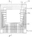
디스플레이 소자의 한 종류인 유기 전계 발광 소자에서는, 도 1에 도시된 바와 같이 기판(1) 상에 픽셀부가 구성되며, 픽셀부를 구성하는 애노드 전극(2) 및 캐소드 전극(4)은 픽셀부의 외측에 형성된 데이터 라인 및 스캔 라인과 각각 연결된다. 데이터 라인과 스캔 라인의 각 단부는 기판(1)의 한 부분으로 집중되어 패드를 형성하게 된다.In the organic electroluminescent element, which is one type of display element, a pixel portion is formed on the
이후, 실란트를 이용하여 캡을 기판(1)에 부착함으로써 픽셀부, 데이터 라인 및 스캔 라인은 외부와 격리된다(미설명 부호 "5"는 캐소드 전극(4)을 분리하기 위한 격벽이다).Thereafter, by attaching the cap to the
유기 전계 발광 소자를 구성하는 각 구성 요소, 특히 애노드 전극(2) 상에 형성된 유기물층(3)은 온도 및 습도에 매우 취약하며, 따라서 외부 환경으로부터 소자 구성 요소를 보호하기 위하여 기판(1)에 캡을 부착한다.Each component constituting the organic electroluminescent device, in particular the
도 1에 도시된 바와 같은 구성 요소가 캡에 의하여 외부와 격리되어 있는 구조를 갖고 있지만, 캡 부착 영역에서의 캡과 기판(1) 사이의 미세 간격을 통하여 외부의 습기 및 산소가 소자 내부 공간(즉, 캡과 기판 사이의 공간)으로 침투하는 것을 완전하게 차단하기는 어렵다.Although the component as shown in FIG. 1 has a structure in which it is isolated from the outside by the cap, the external moisture and oxygen are absorbed through the micro-gap between the cap and the
이와 같은 경로를 통하여 소자 내부 공간으로 침투한 습기 및 산소를 제거하기 위하여 캡의 내부면에 흡습제층(이하, "게터"라 칭함)을 부착한다.A moisture absorbent layer (hereinafter referred to as "getter") is attached to the inner surface of the cap to remove moisture and oxygen that have penetrated into the device internal space through such a path.
화학 재료로 이루어진 게터는 수분과의 화학 반응을 통하여 수분을 흡수하게 되며, 따라서 캡과 기판(1) 사이의 공간에 존재하는 수분이 제거된다. 이와 같은 게터의 흡습 기능에 의하여 소자의 각 구성 요소는 수분에 의한 영향을 받지 않는다.The getter made of a chemical material absorbs moisture through a chemical reaction with moisture, thereby removing moisture present in the space between the cap and the
이와 같은 구조를 갖는 유기 전계 발광 소자의 테스트 과정에서, 캡의 표면에 진동, 충격 등과 같은 외력이 작용할 수 있다. 얇은 두께를 갖는 캡에 외력이 가해질 경우, 캡은 기판(1)을 향하여 눌려지게 된다.In a test process of the organic EL device having such a structure, external forces such as vibration and impact may be applied to the surface of the cap. When an external force is applied to the cap having a thin thickness, the cap is pressed against the
한편, 소자의 대형화를 위해서는 캡의 면적 역시 넓어져야 하며, 이러한 조건에서는 얇은 두께 및 넓은 면적의 캡에서는 자연적인 처짐이 발생하게 된다.On the other hand, in order to increase the size of the device, the area of the cap also needs to be widened, and in such a condition, natural deflection occurs in a thin thickness and a large area of the cap.
이와 같이, 외력에 의하여 캡이 기판(1)을 향하여 눌려지는 경우, 또는 자연적인 처짐에 의하여 캡의 내면에 부착된 게터와 픽셀부의 캐소드 전극(4)이 접촉하게 된다.As described above, when the cap is pressed toward the
화학 재료로 제조된 게터와 금속 재료로 구성된 캐소드 전극(4)의 접촉 부위에서는 화학 반응이 진행된다. 따라서 게터의 높은 화학적 활성도로 인하여 화학 반응이 촉진되어 캐소드 전극(4)이 손상되며, 심한 경우, 캐소드 전극(4)이 기판(1)에서 분리되는 소위 "필링(peeling) 현상"이 발생할 수 있다. 캐소드 전극(4) 의 손상 및 필링 현상은 소자 자체의 기능에 심각한 악영향을 초래하게 된다.A chemical reaction proceeds at the contacting site of the getter made of the chemical material with the
또한, 이러한 필링 현상이 발생되는 경우, 금속 재료로 이루어진 캐소드 전극(4)에서 금속 입자가 생성, 분리된다. 이러한 금속 입자들이 인접한 다른 캐소드 전극들 사이에 위치하게 되며, 따라서 금속 입자들은 캐소드 전속 전극들간의 쇼트를 유발하게 된다.In addition, when such a peeling phenomenon occurs, metal particles are generated and separated from the
이러한, 현상은 격벽(5) 상에 형성된 금속층(도시되지 않음)에서도 동일하게 나타난다.This phenomenon is similarly shown in the metal layer (not shown) formed on the
위와 같은 문제점은 소자에 대한 테스트 과정에서뿐만 아니라, 디스플레이 소자의 운반, 취급 및 사용 과정에서도 동일하게 발생한다.The above problems occur not only during the test process for the device but also during the transport, handling and use of the display device.
본 발명은 흡습제층과 픽셀부의 구성 요소간의 접촉이 일어나지 않도록 구성한 디스플레이 소자를 제공하는데 그 목적이 있다.SUMMARY OF THE INVENTION An object of the present invention is to provide a display element configured such that no contact between the moisture absorbent layer and the components of the pixel portion occurs.
상술한 과제 해결 수단으로 본 발명은, 기판; 기판에 형성된 픽셀부; 기판에 부착되는 제 1 영역 및 제 1 영역의 위치와 상이한 단차를 갖고 제 1 영역에 연결되며 픽셀부와 대응하는 제 2 영역을 포함하는 캡; 캡의 제 2 영역에 위치된 흡습제층; 및 흡습제층에 위치된 보호층을 포함하되, 보호층의 길이는 흡습제층의 길이보다 작거나 보호층의 폭은 흡습제층의 폭보다 작은 디스플레이 소자를 제공한다.The present invention as a problem solving means described above, the substrate; A pixel portion formed on the substrate; A cap including a first region attached to the substrate and a second region connected to the first region having a step different from the position of the first region and corresponding to the pixel portion; A hygroscopic layer located in the second region of the cap; And a protective layer positioned on the absorbent layer, wherein the protective layer has a length smaller than the length of the absorbent layer or a width of the protective layer smaller than the width of the absorbent layer.
본 발명의 일 실시예에서, 보호층은 흡습제층의 폭보다 작은 폭을 갖는다. 특히, 흡습제층과 보호층의 폭의 비율은 10:1 내지 2:1이며, 두께 비율은 10:1 내지 7:1이 바람직하다.In one embodiment of the present invention, the protective layer has a width smaller than the width of the absorbent layer. In particular, the ratio of the width of the absorbent layer and the protective layer is 10: 1 to 2: 1, and the thickness ratio is preferably 10: 1 to 7: 1.
또한, 보호층은 캡의 제 2 영역의 중앙부에 대응하는 영역에서부터 외곽부로 갈수록 그 두께가 증가할 수 있으며, 이와 달리 보호층은 그 두께가 중심부에서 외곽부로 갈수록 점차적으로 증가할 수 있다.In addition, the protective layer may increase in thickness from the region corresponding to the center of the second region of the cap toward the outer portion, whereas the protective layer may gradually increase in thickness from the center portion to the outer portion.
본 발명의 일 실시예에서의 캡을 구성하는 제 2 영역은 단일의 평면부로 이루어지거나, 단차가 다른 복수의 평면부를 포함할 수 있다.The second region constituting the cap in one embodiment of the present invention may consist of a single flat portion or may comprise a plurality of flat portions having different steps.
이하, 본 발명의 실시예에 따른 디스플레이 소자를 첨부한 도면을 통하여 상세히 설명한다. 한편, 이하의 설명에서는 디스플레이 소자의 한 종류인 유기 전계 발광 소자를 예를 들어 설명하였으나, 본 발명은 유기 전계 발광 소자에 한정되는 것은 아니다.Hereinafter, a display device according to an embodiment of the present invention will be described in detail with reference to the accompanying drawings. In the following description, an organic electroluminescent element, which is a type of display element, has been described as an example, but the present invention is not limited to the organic electroluminescent element.
도 2는 본 발명에 따른 디스플레이 소자의 평면도로서, 편의상 기판에 부착된 캡을 도시하지 않았다.Figure 2 is a plan view of the display device according to the present invention, for convenience, does not show a cap attached to the substrate.
도 3은 도 2의 선 B-B을 따라 절취한 상태의 단면도이다. 본 발명에 따른 디스플레이 소자는 다수의 애노드 전극, 애노드 전극 상에 형성된 유기 발광층 및 유기 발광층 상에 형성된 캐소드 전극을 포함하는 픽셀부(100a)를 포함하며, 애노드 전극과 캐소드 전극은 픽셀부(100a) 외측에 형성된 데이터 라인(112) 및 스캔 라인(114)과 각각 연결된다.3 is a cross-sectional view taken along the line B-B of FIG. 2. The display device according to the present invention includes a
데이터 라인(112)과 스캔 라인(114)의 각 단부는 기판(100)의 한 부분으로 집중되어 패드(111)를 형성하거나, 또는 패드를 구성하지 않고 데이터 라인과 스캔 라인의 각 단부가 소자 구동부에 연결될 수 있다.Each end of the
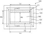
기판(100) 상에 픽셀부(100a) 및 데이터 라인(112)과 스캔 라인(114)을 형성 한 후, 실란트를 이용하여 캡(120)을 기판(100)의 외곽부(113; 이하, "캡 부착 영역"이라 정의함)에 부착함으로써 픽셀부(100a), 데이터 라인(112) 및 스캔 라인(114)은 외부와 격리된다.After forming the
본 발명의 한 실시예에 따른 디스플레이 소자에 사용된 캡(120)은 실란트(도시되지 않음)에 의하여 기판(100)의 캡 부착 영역(113)에 부착되는 제 1 영역(121), 제 1 영역(121)과 상이한 평면상에 위치하고 기판(100)에 형성된 픽셀부(100a)와 대응하는 제 2 영역(122) 및 제 1 영역(121)과 제 2 영역(122)을 연결하는 연결 영역(123)으로 구분된다.The
한편, 도 3에서는 픽셀부(100a)와 대응하는 제 2 영역(122)이 단일의 평면부로 이루어져 있음을 도시하고 있으나, 캡(120)의 형상은 이에 한정되지 않는다. 즉, 제 2 영역(122)은 서로 높이(즉, 픽셀부(100a)로부터의 높이) 차이를 갖는 복수의 평면부를 포함할 수 있다.Meanwhile, although FIG. 3 illustrates that the
본 발명의 한 실시예에 사용된 디스플레이 소자용 캡(120)에서는, 픽셀부(100a)와 대응하는 제 2 영역(122) 내면에 부착된 흡습제층(130; 이하, "게터(getter)"라 정의함)의 일부 영역에 보호층(140)이 형성(부착)된다.In the
한편, 위의 설명 및 도 3에서는 게터(130)가 제 2 영역(122)에 부착된 상태를 도시하고 설명하였지만, 제 1 영역(121)을 제외한 모든 영역에 게터(130)가 부착될 수 있음은 물론이다.Meanwhile, in the above description and FIG. 3, the
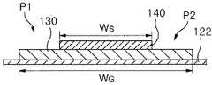
보호층(140)은 게터(130)와 픽셀부(100a)에 형성된 캐소드 전극의 접촉을 차단하는 요소로서, 보호층(140)의 구체적인 형상을 도 4를 통하여 설명한다.The
도 4는 도 3에 도시된 캡(120)의 저면도로서, 게터(130)에 대한 보호층(140)의 형성 위치를 도시하고 있다.FIG. 4 is a bottom view of the
도 5a는 도 4의 선 C-C을 따라 절취한 상태의 단면도로서, 도 5a는 도 4와 일치시키기 위하여 게터(130)의 상부에 보호층(140)이 위치한 상태로 도시하였으며, 또한 캡(120)의 제 2 영역(122)의 일부만을 도시하였다.FIG. 5A is a cross-sectional view taken along the line CC of FIG. 4, and FIG. 5A is a view showing the
한편, 이하의 설명에서는, 보호층(140) 및 게터(130)의 가로 방향 길이(Ls및 LG)를 "길이"로, 세로 방향 길이(Ws및 WG)를 "폭"으로 정의한다.In the following description, the horizontal length Ls of the
전술한 바와 같이, 캡(120)의 제 2 영역(122)의 내면에는 게터(130)가 부착되어 있으며, 보호층(140)은 게터(130)의 소정 영역에 부착된다.As described above, the
본 발명의 일 실시예에서는, 보호층(140)은 그 길이(Ls)가 게터(130)의 길이(LG)와 동일하며, 폭(Ws)는 게터(130)의 폭(WG)보다는 작다. 따라서, 도 4에 도시된 바와 같이, 게터(130)의 외곽부 중 일정 면적의 상부 및 하부 영역(도 4 기준; P1 및 P2)만이 보호층(140)과 대응하지 않은 상태에서 외부로 노출된다.In an embodiment of the present invention, the
한편, 게터(130)의 흡습 기능에 영향을 미치지 않는 범위 내에서 보호층(140)의 폭(즉, 면적)이 결정된다. 제한되지는 않으나, 본 발명의 다른 실시예에 따른 캡에서, 게터(130)의 폭에 대한 보호층(140)의 폭의 비율(즉, WG:Ws)은 10:1 내지 2:1의 범위이다. 이에 대한 구체적인 이유는 추후 설명한다.On the other hand, the width (that is, area) of the
만일 게터(130)의 폭에 대한 보호층(140)의 폭의 비율이 10:1보다 클 경우, 보호층(140)의 면적이 지나치게 좁게되며, 따라서 보호층(140)은 그 기능, 즉 게 터(130)와 픽셀부(100a)의 접촉 방지 기능을 효과적으로 수행할 수 없다.If the ratio of the width of the
반대로, 게터(130)의 폭에 대한 보호층(140)의 폭의 비율이 2:1보다 작을 경우, 보호층(140)의 면적이 상대적으로 넓어지게 되며, 이러한 조건에서는 보호층(140)이 게터(130)의 표면 대부분을 덮기 때문에 게터(130)의 흡습 기능을 저하시키게 된다. 그러나, 위와 같은 조건에서도 보호층(140)의 두께가 얇을 경우, 수분이 보호층(140)을 뚫고 게터(130)에 흡수될 수 있다. 또한 보호층(140)을 투수성을 갖는 재료로 구성하는 경우에도 수분이 소정의 두께를 갖는 보호층(140)을 통과하여 게터(130)에 흡수될 수 있다.On the contrary, when the ratio of the width of the
위와 같은 조건 하에서의 게터(130)에 부착된 보호층(140)의 기능을 도 3 및 도 4를 통하여 설명하면 다음과 같다.The function of the
유기 전계 발광 소자의 테스트 과정 또는 취급 과정에서, 얇은 두께를 갖는 캡(120)에 진동, 충격 등과 같은 외력이 가해질 경우 또는 자연적인 처짐에 의하여 캡(120), 특히 비교적 넓은 면적의 제 2 영역(122)은 기판(100)을 향하여 눌려지게 된다(도 3의 점선 L2).In the test or handling process of the organic EL device, when the external force such as vibration or shock is applied to the
그러나, 캡(120)의 제 2 영역(122)이 픽셀부(100a)를 향하여 눌려지거나 처질지라도 게터(130)는 그 표면에 부착된 보호층(140)에 의하여 픽셀부(100a)의 캐소드 전극과 접촉되지 않는다.However, even if the
이와 같이, 보호층(140)에 의하여 금속 재료로 이루어진 캐소드 전극과 화학 물질인 게터(130)의 직접적인 접촉이 방지됨으로써 캐소드 전극은 손상되지 않는다. 한편, 캐소드 전극과 보호층(140)이 서로 접촉할지라도 보호층(140)이 절연성 (비전도성) 재료로 구성되어 있기 때문에 인접한 캐소드 전극 간에 쇼트(short)는 일어나지 않는다. 또한, 절연성 재질의 보호층(140)은 그 거칠기 및 강도가 금속보다 작기 때문에 접촉하는 캐소드 전극이 손상되는 현상이 발생되지 않는다.As such, since the direct contact between the cathode electrode made of a metal material and the
이러한 형상의 보호층(140)이 부착될지라도 게터(130)는 그 외곽 부분(P1 및 P2)이 노출되며, 따라서 캡 부착 영역(113)을 통하여 유입되는 수분(실란트에 함유된 수분 포함)이 곧바로 게터(130)에 흡수된다. 또한, 위에서 설명한 바와 같이, 보호층(140)의 두께가 얇거나, 보호층(140)이 투수성을 갖는 절연성 재료로 이루어진 경우, 소자 내부에 존재하는 수분은 보호층(140)을 뚫고 게터(130)에 흡수된다.Even when the
보호층(140)의 위와 같은 기능들, 즉 게터(130)와 픽셀부(100A)에 형성된 캐소드 전극 간의 접촉 억제, 캐소드 전극 간의 쇼트 발생 방지 및 게터(130)의 흡습 기능 유지를 위하여 보호층(140)을 전기적 절연성 및 투수성을 갖는 에폭시 계열의 재료 또는 폴리이미드(polyimide)로 구성하는 것이 바람직하다.The
이러한 물리적 특성을 갖는 에폭시 계열의 재료로서, 제한되지는 않지만, 기능성 모노머(monomer)인 트리메틸 프로판 트리아크릴레이트(TMPTA; trimethylolpropane triacrylate)와 에폭시 아크릴레이트(expoxy arylate)의 혼합물, 1,4-부탄디올 디글리시딜 에테르 디아크릴레이트(1,4-BDGEDA; butanediol diglycidyl ether diacrylate), 폴리부타디엔(polybutadien), 폴리부타디엔 아클릴레이트(polybutadien acrylate) 또는 폴리에틸렌 글리콜 디아크릴레이트(PEGDA; polyethylene glycol diacrylate)를 예를 들 수 있다.Epoxy-based materials having these physical properties include, but are not limited to, a mixture of trimethyl propane triacrylate (TMPTA) and an epoxy acrylate (1,4-butanediol di), which are functional monomers (trimethylolpropane triacrylate). Examples of glycidyl ether diacrylate (1,4-BDGEDA; butanediol diglycidyl ether diacrylate), polybutadien, polybutadiene acrylate, or polyethylene glycol diacrylate (PEGDA) Can be mentioned.
도 5b는 도 5a의 대응 도면으로서, 본 발명의 다른 실시예에 따른 디스플레 이 소자에서의 보호층을 도시한 단면도이다. 위에서 설명한 바와 같이, 투수성을 갖는 재료로 이루어진 보호층을 형성함과 동시에 도 5b에 도시된 바와 같이 보호층(240)을 관통하는 적어도 하나의 개구(241)를 형성하는 경우, 수분이 이 개구(241)를 직접적으로 통과하여 게터(130)에 도달함으로써 게터(130)의 흡습 기능이 더욱 향상된다.FIG. 5B is a corresponding view of FIG. 5A and is a cross-sectional view illustrating a protective layer in the display device according to another embodiment of the present invention. FIG. As described above, when forming a protective layer made of a material having water permeability and at least one
특히, 보호층(240)이 투수성이 없는 재료로 이루어진 경우에도 수분은 각 관통 개구(241)를 통과하여 게터(130)에 도달하기 때문에 게터(130)에 의한 흡습 효과를 충분히 얻을 수 있음은 물론이다.In particular, even when the
한편, 보호층(140 또는 240)은 디스플레이 소자의 규격에 따라 그 폭 및 두께를 다양하게 결정할 수 있다. 즉, 게터(130)와 픽셀부(100a; 즉, 캐소드 전극) 간에 소정의 간격이 유지되는 범위 내에서 보호층(140 또는 240)의 두께를 결정하여야 하며, 또한 게터(130)의 흡습 및 산소 흡수 기능에 영향을 주지 않는 범위 내에서 그 폭을 결정한다. 이에 대한 설명은 추후 설명한다.Meanwhile, the
여기서, 위에서 설명한 바와 같이, 캡(120)에 외력이 가해질 때 처짐량이 가장 크게 나타나는 제 2 영역(122)의 중심부와 보호층(140, 240)의 중심부가 대응하도록 보호층(140 또는 240)을 게터(130)에 형성(또는 부착)하는 것이 바람직하다.As described above, when the external force is applied to the
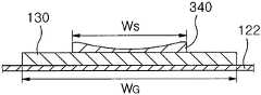
도 5c는 도 5a의 대응 도면으로서, 본 발명의 또 다른 실시예에서의 보호층(340)을 도시한 단면도이다. 도 5c에 도시된 보호층(340)의 구성적인 특징은 위치에 따라 그 두께를 달리한 것이다.5C is a cross-sectional view of the
도 4에 도시된 바와 같이, 캡(120)의 제 2 영역(122)의 전체 영역 중에서 변 형량이 가장 크게 나타나는 부분은 중앙부이다. 따라서 제 2 영역(122)에 큰 외력이 작용하는 경우, 제 2 영역(122)의 중앙부에 대응하는 보호층이 픽셀부(도 4의 100a)를 과도한 압력으로 누르게 되며, 이로 인하여 픽셀부(100a)를 구성하는 요소가 압력에 의하여 손상될 우려가 있다.As shown in FIG. 4, a portion where the deformation amount is greatest in the entire region of the
이를 방지하기 위하여, 즉 보호층과 픽셀부의 과도한 접촉을 방지하기 위하여 도 5c에 도시된 바와 같이 보호층(340)은 제 2 영역(122)의 중앙부에 대응하는 중앙 부분에서부터 외곽부로 갈수록 그 두께가 점차적으로 증가되는 형상을 갖는 것이 가능하다.In order to prevent this, that is, to prevent excessive contact between the protective layer and the pixel portion, as shown in FIG. 5C, the
이러한 형상의 보호층(340)에서는 캡(120)의 제 2 영역(122)의 중앙부가 과도하게 변형, 즉 픽셀부(100a)를 향하여 과도하게 처지는 경우에도 보호층(340)의 대응 영역은 픽셀부(100a)에 접촉하지 않는다. 따라서 픽셀부(100a)를 구성하는 구성 요소가 압력에 의하여 손상되는 문제점은 발생하지 않는다.In the
도 5d는 도 5a의 대응 도면으로서, 또 다른 형상의 보호층을 도시한 단면도이다. 도 5c에 도시된 보호층(340)과 달리, 도 5d에 도시된 보호층(340a)은 그 중심이 캡(120), 특히 제 2 영역(122)의 중앙부(Ca)와 일치하지 않은 상태로 게터(130)에 부착되어 있다. 이와 같은 상태에서 보호층(340a)은 캡(120)의 제 2 영역(122)의 중앙부에 대응하는 영역에서부터 외곽부로 갈수록 그 두께가 증가한다.FIG. 5D is a sectional view of FIG. 5A, showing a protective layer in yet another shape. Unlike the
도 6은 본 발명의 다른 실시예에 사용된 보호층의 또 다른 형상을 도시한 캡의 저면도로서, 다각형, 예를 들어 사각형 보호층(440)의 에지(edge)가 게터(130) 상에 위치하고 있음을 도시하고 있다. 이러한 보호층(440)에 의하여 게터(130)의 모든 외곽부는 외부로 노출된다.FIG. 6 is a bottom view of a cap showing another shape of a protective layer used in another embodiment of the present invention, wherein an edge of a polygonal, eg, rectangular
캡(120)에 작용하는 외력에 의하여 제 2 영역(122)이 기판(100)을 향하여 눌려지는 경우, 수평면이 아닌 경사진 구조의 연결부(123)는 지지대의 기능을 수행하게 되며, 따라서 제 2 영역(122)의 외곽부에는 외력이 거의 작용하지 않는다.When the
이러한 조건에 의하여, 도 3의 점선 "L2"로 나타낸 바와 같이, 캡(120)의 제 2 영역(122)의 중앙부에서 가장 큰 양의 눌려짐(처짐)이 나타나며, 외곽부로 갈 수록 눌려짐 양의 줄어든다.Under these conditions, as indicated by the dotted line “L2” in FIG. 3, the greatest amount of depression (sag) appears at the center of the
따라서, 도 6에서와 같이 게터(130)의 영역 중에서, 외곽부를 제외한 영역, 즉 캡(120)의 제 2 영역(122)의 중앙부(즉, 눌려짐이 가장 크게 나타나는 부분)와 대응하는 영역에만 보호층(440)을 형성하더라도, 게터(130)와 픽셀부(100a)의 캐소드 전극 간의 접촉을 완전하게 방지할 수 있다. 즉, 위와 같은 조건을 만족한다면, 보호층(440)의 각 에지부의 위치는 제한되지는 않는다.Therefore, as shown in FIG. 6, only the region excluding the outer portion of the
이러한 점을 고려하여, 게터(130)에 부착되는 보호층의 형상을 결정하였다. 즉, 도 6에 도시된 바와 같이, 게터(130)에 부착된 보호층(440)은 그 길이 및 폭이 게터(130)의 길이 및 폭보다 작다. 따라서, 게터(130)의 전체 외곽부는 보호층(440)과 대응하지 않고 외부로 노출된다.In consideration of this point, the shape of the protective layer attached to the
도 4에 도시된 보호층(140)과 비교하여, 보호층(440)의 형성 면적을 최소화함으로써 보호층(440)에 의하여 게터(130)의 기능, 즉 흡습 기능이 제한되는 것을 방지할 수 있다. 즉, 게터(130)와 픽셀부(100a)의 캐소드 간의 접촉을 방지하기 위한 보호층(440)의 형성 면적을 최소화함으로써 게터(130)의 흡습 작용을 최대로 유 지할 수 있는 것이다.Compared to the
여기서, 위에서 설명한 바와 같이, 캡(120)에 외력이 가해질 때 처짐량이 가장 크게 나타나는 제 2 영역(122)의 중심부와 보호층(440)의 중심부가 대응하도록 보호층(440)을 게터(130)에 형성하는 것이 바람직하다. 한편, 도 6에 도시된 보호층(440)의 기능은 도 4에 도시된 보호층(140)의 기능과 동일하며, 따라서 이에 대한 설명은 생략한다.Here, as described above, the
여기서, 각 도면 및 이에 대한 설명에서는, 보호층(140, 240, 340, 340a 및 440)이 단일의 연속적인 층으로 형성되어 있음을 도시하고 설명하고 있으나, 보호층의 구성은 이에 제한되지 않는다. 즉, 선택된 재료를 이용하여 2층 이상의 복층 구조로 보호층을 형성할 수 있음은 물론이다.Here, in the drawings and descriptions thereof, the
이하, 본 발명에 따른 구체적인 실시예를 설명한다.Hereinafter, specific embodiments according to the present invention will be described.
[실시예]EXAMPLE
도 4에 도시된 구조를 갖는 유기 전계 발광 소자용 캡을 제조하였으며, 그 구체적인 조건은 하기 표 1과 같다.A cap for an organic electroluminescent device having a structure shown in FIG. 4 was prepared, and specific conditions thereof are as shown in Table 1 below.
상기 표 1에 기재된 비교예, 실시예 1 및 실시예 2에 따른 소자 20개, 24개 및 24개를 각각 선정한 후, 소자의 캡에 5kg, 10kg, 15kg 및 20kg의 하중을 각각 가였다.After selecting 20, 24 and 24 elements according to Comparative Example, Example 1 and Example 2 described in Table 1, respectively, loads of 5 kg, 10 kg, 15 kg and 20 kg were applied to the caps of the elements, respectively.
캡에 가해진 하중을 제거한 후, 각 소자에 대한 라인 불량(line defect) 여부에 대한 검사를 실시하였으며, 그 검사 결과는 하기 표 2와 같다.After removing the load applied to the cap, each device was inspected for line defects, and the test results are shown in Table 2 below.
* : 위의 결과에서, 비교예에 따른 제 1 및 제 2 소자는 캡에 15kg의 힘을 가한 후 실시한 측정 검사 결과 모두 라인 불량으로 판정되었으며, 따라서 비교예에 따른 잔여 소자들에 대해서는 15kg 및 20kg의 하중을 가하는 실험을 생략하였다.*: In the above results, the first and the second device according to the comparative example was determined to be a line defect in the measurement test performed after applying a force of 15 kg to the cap, and therefore 15kg and 20kg for the remaining elements according to the comparative example The experiment to apply the load of was omitted.
X : 위의 표에서 "X"는 해당 소자가 라인 불량 없이 정상적으로 발광하고 있음을 의미한다.X: "X" in the above table means that the device is normally emitting light without a defective line.
표 2에 기재된 "라인 불량"은 게터와 금속 전극(캐소드 전극)의 접촉으로 인하여 금속 전극이 손상 또는 기판에서 분리되었음을 나타내며, 이는 소자에 대한 점등 검사시 손상된 금속 전극에 대응하는 픽셀이 정상적으로 발광하지 않았음을 것을 의미한다.The "line defect" described in Table 2 indicates that the metal electrode is damaged or separated from the substrate due to the contact of the getter and the metal electrode (cathode electrode), which indicates that the pixel corresponding to the damaged metal electrode does not emit light normally during the lighting inspection of the device. It means not.
표 2를 통하여 알 수 있듯이, 본 발명의 실시예 1 및 실시예 2에 따라 제조된 12개의 모든 소자에서는 10kg 및 15kg의 하중이 작용하는 경우에도 라인 불량이 발생하지 않았으며, 특히 20kg의 하중이 작용하는 경우에도 약 16%(12개 소자중 2개 소자)의 매우 낮은 라인 불량율이 발생하였다.As can be seen from Table 2, in all 12 devices manufactured according to Examples 1 and 2 of the present invention, even if the load of 10kg and 15kg is applied, no line defects occurred, in particular, the load of 20kg Even in operation, a very low line failure rate of about 16% (two out of twelve) occurred.
이러한 결과는 본 발명의 실시예 1 및 실시예 2에 따라 제조된 소자에서, 보호층에 의하여 게터와 금속 전극의 접촉이 이루어지지 않아 금속 전극의 손상 및 들뜸 현상이 크게 개선되었음을 의미한다.These results indicate that in the devices manufactured according to Examples 1 and 2 of the present invention, the getter is not in contact with the metal electrode by the protective layer, thereby greatly improving the damage and lifting of the metal electrode.
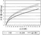
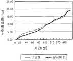
도 7 내지 도 9는 비교예와 실시예 1 및 2에 대한 흡습 기능 및 산소 흡수 기능을 측정한 결과를 나타낸 그래프도로서, 각 도면에 대하여 구체적으로 설명한다.7 to 9 are graphs showing the results of measuring the moisture absorption function and the oxygen absorption function for Comparative Examples and Examples 1 and 2, and the respective drawings will be described in detail.
도 7a는 25℃의 온도 및 60%의 습도 조건 하에서 실시예 1에 따른 6개 소자에서의 평균 흡습 속도 및 비교예에 따른 5개 소자에서의 평균 흡습 속도를 나타낸 그래프로서, 점선은 정상 소자임을 판단하는 기준 흡습 속도를 나타낸다.7A is a graph showing the average moisture absorption rate in the six devices according to Example 1 and the average moisture absorption rate in five devices according to the comparative example under the temperature of 25 ℃ and 60% humidity conditions, the dotted line is a normal device The standard moisture absorption rate to be judged is shown.
도 7b는 25℃의 온도 및 60%의 습도 조건 하에서 실시예 2에 따른 6개 소자에서의 평균 흡습 속도 및 비교예에 따른 5개 소자에서의 평균 흡습 속도를 나타낸 그래프로서, 점선은 정상 소자임을 판단하는 기준 흡습 속도를 나타낸다.7B is a graph showing the average moisture absorption rate in the six devices according to Example 2 and the average moisture absorption rate in five devices according to the comparative example under the temperature of 25 ℃ and 60% humidity conditions, the dotted line is a normal device The standard moisture absorption rate to be judged is shown.
도 7a 및 도 7b에서는 실시예 1 및 2에 따른 소자에서의 흡습 속도가 비교예에 따른 소자에서의 흡습 속도 및 기준 흡습 속도보다는 낮게 나타난다.7A and 7B, the moisture absorption rate in the device according to Examples 1 and 2 is lower than the moisture absorption rate and the reference moisture absorption rate in the device according to the comparative example.
도 8a는 가혹 조건인 32℃의 온도 및 83%의 습도 조건 하에서 실시예 1에 따른 6개 소자에서의 누적 흡습량 및 비교예에 따른 5개 소자에서의 누적 흡습량을 나타낸 그래프로서, 시간 경과에 따른 누적 흡습량의 변화 상태를 나타낸다.FIG. 8A is a graph showing the cumulative moisture absorption in the six devices according to Example 1 and the cumulative moisture absorption in the five devices according to the comparative example under a temperature of 32 ° C. and a humidity of 83% under severe conditions. The change state of the cumulative moisture absorption amount is shown.
또한, 도 8b는 32℃의 온도 및 83%의 습도 조건 하에서 실시예 2에 따른 6개 소자에서의 누적 흡습량 및 비교예에 따른 5개 소자에서의 누적 흡습량을 나타낸 그래프이다.,8B is a graph showing the cumulative moisture absorption in the six devices according to Example 2 and the cumulative moisture absorption in the five devices according to the comparative example under the temperature of 32 ° C. and the humidity of 83%.
도 8a 및 도 8b에 도시된 바와 같이, 비교예에 따른 소자와 비교하여 실시예 1 및 2에 따른 소자들은 초기에는 누적 흡습량이 적지만, 시간이 경과함에 따라, 즉 약 450분 이후에는 비교예에 따른 소자와 누적 흡습량에 있어서 차이가 없음을 알 수 있다. 이는 표면에 보호층이 부착되어 있음에도 불구하고 게터가 흡습 기능을 정상적으로 수행하고 있음을 나타낸다.As shown in FIGS. 8A and 8B, the devices according to Examples 1 and 2 are initially less cumulative moisture absorption compared to the devices according to the comparative example, but as time passes, that is, after about 450 minutes It can be seen that there is no difference in the device and the cumulative moisture absorption according to. This indicates that the getter normally performs the hygroscopic function even though the protective layer is attached to the surface.
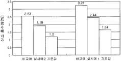
각 소자의 산소 흡수 능력을 표시한 도 9의 좌측부는 실시예 2에 따른 소자를 구성하는 게터(보호층이 부착된 상태임) 5개 및 비교예에 따른 소자를 구성하는 게터(보호층이 부착되지 않은 상태임) 5개를 80℃의 온도 및 약 4%의 산소 분위기의 바이알 내부에 24시간 동안 위치시킨 후 측정한 평균 산소 흡수량을 측정한 결과를 나타낸다. 여기서, 도 9의 좌측부에 기재된 기준값 1.2는 8mm×14mm 규격의 게터가 기본적으로 흡수해야만하는 기준 산소 흡수량을 나타낸다.On the left side of FIG. 9 showing the oxygen absorption capability of each device, five getters (with a protective layer attached) constituting the device according to Example 2 and getters (protective layer attached) constituting the device according to the comparative example Not shown) and the average oxygen uptake measured after placing five in a vial at a temperature of 80 ° C. and an oxygen atmosphere of about 4% for 24 hours. Here, the reference value 1.2 described in the left part of FIG. 9 indicates the reference oxygen absorption amount that the getter of 8 mm x 14 mm standard should be absorbed basically.
도 9에서, 우측부는 실시예 1에 따른 소자를 구성하는 게터(보호층이 부착된 상태임) 5개 및 비교예에 따른 소자를 구성하는 게터(보호층이 부착되지 않은 상태임) 5개를 80℃의 온도 및 약 4%의 산소 분위기의 바이알 내부에 24시간 동안 위치시킨 후 측정한 평균 산소 흡수량을 측정한 결과를 나타낸다. 여기서, 도 9의 우측부에 기재된 기준값 1.64는 9mm×17mm 규격의 게터가 기본적으로 흡수해야만하는 기준 산소 흡수량을 나타낸다.In FIG. 9, the right portion includes five getters (with a protective layer attached) constituting an element according to Example 1 and five getters (with a protective layer not attached) constituting an element according to a comparative example. The result of measuring the average oxygen absorption amount measured after placing for 24 hours in the vial of 80 degreeC temperature and about 4% of oxygen atmosphere is shown. Here, reference value 1.64 described in the right part of FIG. 9 indicates a reference oxygen absorption amount that a 9 mm x 17 mm standard getter should basically absorb.
한편, 도 9의 좌측부 및 우측부에서 비교예의 산소 흡수량 및 기준 산소 흡수량은 어느 정도 차이가 있다. 이러한 차이는 시간 간격을 두고 실시되는 각 실험의 조건, 예를 들어 산소 함유량(체적 비율)의 차이에 의하여 나타난다.On the other hand, the oxygen absorption amount and the reference oxygen absorption amount of the comparative example are somewhat different in the left and right portions of FIG. 9. This difference is indicated by the difference in the conditions of each experiment conducted at time intervals, for example, the oxygen content (volume ratio).
도 9에서 알 수 있는 바와 같이, 본 발명의 제 1 및 제 2 실시예에 적용된 게터는 그 산소 흡수량이 비교예에 적용된 게터의 산소 흡수량보다 0.6%(실시예 2) 내지 0.7%(실시예 1)보다 작게 나타나지만, 기준 산소 흡수량을 크게 초과한다. 이는, 표면에 보호층이 부착되어 있음에도 불구하고 게터가 산소 흡수 기능을 정상적으로 수행하고 있음을 나타낸다.As can be seen in Figure 9, the getter applied to the first and second embodiments of the present invention is 0.6% (Example 2) to 0.7% (Example 1) than the oxygen absorption amount of the getter applied to the comparative example It appears smaller than), but greatly exceeds the reference oxygen uptake. This indicates that the getter performs the oxygen absorption function normally even though the protective layer is attached to the surface.
게터에 보호층이 부착되어 있음에도 불구하고 본 발명의 제 1 및 제 2 실시예에 따른 소자에서는 흡습 및 산소 흡수라는 게터의 기본적인 기능이 보호층에 의하여 큰 영향을 받지 않고 않음을 도 7, 도 8 및 도 9를 통하여 알 수 있다.Although the protective layer is attached to the getter, the basic functions of the getter, such as moisture absorption and oxygen absorption, are not largely affected by the protective layer in the devices according to the first and second embodiments of the present invention. And it can be seen through FIG.
이하의 설명에서는 실시예 2에 나타난 소자를 통하여 게터와 보호층의 폭 및 두께의 비율 관계에 대하여 설명한다.In the following description, the ratio relationship between the width and thickness of the getter and the protective layer will be described through the device shown in Example 2.
게터의Getter's 두께와 보호층의 두께의 관계 Relationship between the thickness and the thickness of the protective layer
표 1에 설명된 실시예 2에 다른 소자에서는 금속 캡의 규격이 44mm×32.75mm이며, 캡에 부착된 게터의 규격은 8mm(폭)×14mm(길이)×0.3mm(두께)이다.In the device other than Example 2 described in Table 1, the size of the metal cap is 44 mm x 32,75 mm, and the size of the getter attached to the cap is 8 mm (width) x 14 mm (length) x 0.3 mm (thickness).
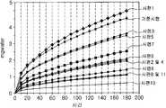
이와 같은 규격의, 보호층이 부착되지 않은 게터 및 서로 다른 두께 및 폭을 갖는 10개의 보호층이 각각 부착된 게터 등, 총 11개의 게터(이하, "시편"이라 칭함)를 이용하여 흡습 실험을 실시하였으며, 시간 경과에 따른 각 시편의 흡습량의 변화를 도 10의 그래프로 나타내었다.A hygroscopic experiment was carried out using a total of eleven getters (hereinafter referred to as "test specimens") such as a getter without a protective layer and a getter with ten protective layers having different thicknesses and widths, respectively. The change in moisture absorption amount of each specimen with time is shown in the graph of FIG. 10.
본 실험에 사용된 게터에 부착된 보호층의 규격(두께 및 폭의 비율)은 하기의 표 3과 같다.Specifications of the protective layer (thickness and width ratio) attached to the getter used in this experiment are shown in Table 3 below.
한편, 시편 1은 보호층이 부착되지 않은 게터를 나타내며, 도 10에서의 "기준 시편"은 최적의 흡습량을 갖는 기준 시편(게터)을 의미한다. 여기서, 기준 시편의 흡습량의 약 80% 정도의 흡습량을 가질 경우 게터가 정상적인 흡습 기능을 갖는 것으로 간주된다.Meanwhile,
한편, 도 11는 도 10의 그래프에서 각 시간에서의 각 시편의 흡습량을 수치화한 비교표로서, 도 10 및 도 11에 나타난 바와 같이, 최적의 흡습량을 갖는 "기준 시편"의 흡습량에 가장 인접한 흡습량을 갖는 시편은 "시편 3" 및 "시편 5"으로서, 각 시편은 흡습 실험 180분 후에 기준 시편의 흡습량(즉, 약 4.5 mgWater)의 80% 정도의 흡습량(3.48 내지 3.59 mgWater)을 나타낸다.Meanwhile, FIG. 11 is a comparison table quantifying the moisture absorption amount of each specimen at each time in the graph of FIG. 10. As shown in FIGS. 10 and 11, the moisture absorption amount of the “reference specimen” having the optimal moisture absorption amount is most shown in FIG. 10. Specimens with adjacent moisture absorptions were "
시편 3 및 시편 5에서의 게터의 두께에 대한 보호층의 두께 백분율은 10% 및 15%이다.The thickness percentages of the protective layer relative to the thickness of the getter in
도 10 및 도 11에 나타난 결과를 통하여, 게터의 두께에 대한 보호층의 두께 백분율이 10% 내지 15%(즉, 게터의 두께에 대한 보호층의 두께 비율은 10:1 내지 7:1)가 가장 바람직한 것임을 알 수 있다.10 and 11, the percentage of the thickness of the protective layer to the thickness of the getter is 10% to 15% (ie, the ratio of the thickness of the protective layer to the thickness of the getter is 10: 1 to 7: 1). It can be seen that most preferred.
한편, 게터의 두께의 10% 및 15%의 두께를 갖는 "시편 2" 및 "시편 4"는 동일한 두께를 갖고 있음에도 불구하고 "시편 3" 및 "시편 5"과 비교하여 흡습량이 현저하게 낮은 상태로 나타난다.On the other hand, "
이러한 결과는 게터의 폭에 대한 보호층의 폭의 비율에 따라 게터의 흡습량이 변화한다는 것을 나타내는 것으로서, 게터의 폭에 대한 보호층의 폭의 백분율 변화에 대한 흡습량 변화 실험 결과를 도 12 및 도 13을 이용하여 설명한다.These results indicate that the moisture absorption amount of the getter changes according to the ratio of the width of the protective layer to the width of the getter. It demonstrates using 13.
게터의Getter's 폭과 보호층의 폭의 관계 Relationship between width and width of protective layer
도 10의 결과를 통하여 게터의 두께에 대한 보호층의 두께 백분율이 10% 및 15%인 경우, 게터가 최적의 흡습 기능을 갖고 있음을 알 수 있었다. 이러한 최적의 두께 비율 중에서 15%의 두께 비율을 유지한 상태에서 게터의 폭에 대한 보호층의 폭의 백분율을 달리하여 게터의 흡습 실험을 실시하였으며, 그 결과를 도 111에 도시하였다.10, it can be seen that the getter has an optimal moisture absorption function when the thickness percentages of the protective layer to the thickness of the getter are 10% and 15%. The moisture absorption experiment of the getter was performed by varying the ratio of the width of the protective layer to the width of the getter while maintaining the thickness ratio of 15% among the optimum thickness ratios, and the results are shown in FIG. 111.
규격이 8mm(폭)×14mm(길이)×0.3mm(두께) 규격의, 보호층이 부착되지 않은 게터 및 두께는 동일하지만 폭이 서로 다른 10개의 보호층이 각각 부착된 게터 등, 총 11개의 게터(이하, "시편"이라 칭함)를 이용하여 흡습 실험을 실시하였으며, 시간 경과에 따른 각 시편의 흡습량의 변화를 도 12에 도시하였다.A total of 11, including getters with 8 mm (width) × 14 mm (length) × 0.3 mm (thickness) dimensions, without getters and 10 getters with the same thickness but 10 different widths. A moisture absorption experiment was conducted using a getter (hereinafter referred to as a "test piece"), and FIG. 12 shows a change in moisture absorption amount of each test piece over time.
본 실험에 사용된 게터에 부착된 보호층의 규격(두께 및 폭)은 하기의 표 4와 같다.The specifications (thickness and width) of the protective layer attached to the getter used in this experiment are shown in Table 4 below.
한편, 본 실험에서의 기준 시편 1은 보호층이 부착되지 않은, 최적의 흡습량을 갖는 게터를 나타내며, 도 12의 그래프에서 "기준 시편"으로 표시하였다. 여기서, 기준 시편의 흡습량의 약 80% 정도의 흡습량을 가질 경우 게터가 정상적인 흡습 기능을 갖는 것으로 간주된다.On the other hand, the
한편 도 13은 도 12의 그래프에서 각 시간에서의 각 시편의 흡습량을 수치화한 비교표이다.On the other hand, Figure 13 is a comparison table that the numerical value of the moisture absorption of each specimen at each time in the graph of FIG.
도 12 및 도 13을 통하여 알 수 있는 바와 같이, 최적의 흡습량을 갖는 "기준 시편"의 흡습량에 가장 근접한 흡습량을 갖는 시편은 시편 6, 7, 8, 9 및 10으로서, 각 시편은 흡습 실험 180분 후에 기준 시편의 흡습량(즉, 약 4.5 mgWater)의 80% 정도의 흡습량(3.7523 내지 4.29923 mgWater)을 나타낸다..As can be seen from FIGS. 12 and 13, the specimens having the moisture absorption amount closest to the moisture absorption amount of the “reference specimen” having the optimum moisture absorption are
시편 6, 7, 8, 9 및 10에서의 게터의 폭에 대한 보호층의 폭의 백분율은 각각 50%, 40%, 30%, 20% 및 10%로서, 본 실험 결과를 통하여 게터의 폭에 대한 보호층의 폭의 백분율이 10% 내지 50%(즉, 게터의 폭에 대한 보호층의 폭의 비율은 2:1 내지 10:1)가 가장 바람직한 것임을 알 수 있다.The percentage of protective layer width to getter width in
위에서 설명한 본 발명의 바람직한 실시예는 예시의 목적을 위해 개시된 것이고, 본 발명에 대한 통상의 지식을 가지는 당업자라면 본 발명의 사상과 범위 안에서 다양한 수정, 변경, 부가가 가능할 것이며, 이러한 수정, 변경 및 부가는 하기의 특허청구범위에 속하는 것으로 보아야 할 것이다.Preferred embodiments of the present invention described above are disclosed for purposes of illustration, and those skilled in the art having various ordinary knowledge of the present invention may make various modifications, changes, and additions within the spirit and scope of the present invention. Additions should be considered to be within the scope of the following claims.
이상과 같은 본 발명은 캡에 외력이 작용할 때, 또는 자연적인 처짐으로 인한 캡의 눌려짐으로 인하여 야기되는 흡습제층과 금속 전극 간의 직접적인 접촉을 흡습제층 표면에 부착된 보호층를 통하여 방지할 수 있으며, 이로 인해 디스플레이 소자의 기능 면에서 안정성을 확보할 수 있다.The present invention as described above can prevent the direct contact between the absorbent layer and the metal electrode caused by the external force applied to the cap, or the cap due to the natural sag through the protective layer attached to the surface of the absorbent layer, This ensures stability in terms of the function of the display element.
Claims (17)
Translated fromKoreanPriority Applications (6)
| Application Number | Priority Date | Filing Date | Title |
|---|---|---|---|
| KR1020060103658AKR100826011B1 (en) | 2006-10-24 | 2006-10-24 | Display elements |
| EP06025587.4AEP1916724B1 (en) | 2006-10-24 | 2006-12-11 | Display device |
| US11/637,775US8319423B2 (en) | 2006-10-24 | 2006-12-13 | Display device with protecting layer for getter layer |
| CN200610170073ACN100576560C (en) | 2006-10-24 | 2006-12-18 | Display device |
| JP2006344579AJP4897468B2 (en) | 2006-10-24 | 2006-12-21 | Display element |
| TW096100034ATWI358962B (en) | 2006-10-24 | 2007-01-02 | Display device |
Applications Claiming Priority (1)
| Application Number | Priority Date | Filing Date | Title |
|---|---|---|---|
| KR1020060103658AKR100826011B1 (en) | 2006-10-24 | 2006-10-24 | Display elements |
Publications (1)
| Publication Number | Publication Date |
|---|---|
| KR100826011B1true KR100826011B1 (en) | 2008-04-29 |
Family
ID=38283242
Family Applications (1)
| Application Number | Title | Priority Date | Filing Date |
|---|---|---|---|
| KR1020060103658AActiveKR100826011B1 (en) | 2006-10-24 | 2006-10-24 | Display elements |
Country Status (6)
| Country | Link |
|---|---|
| US (1) | US8319423B2 (en) |
| EP (1) | EP1916724B1 (en) |
| JP (1) | JP4897468B2 (en) |
| KR (1) | KR100826011B1 (en) |
| CN (1) | CN100576560C (en) |
| TW (1) | TWI358962B (en) |
Cited By (1)
| Publication number | Priority date | Publication date | Assignee | Title |
|---|---|---|---|---|
| KR20140144950A (en)* | 2013-06-12 | 2014-12-22 | 엘지전자 주식회사 | Organic electro-luminescent device display and method for manufacturing the same |
Families Citing this family (2)
| Publication number | Priority date | Publication date | Assignee | Title |
|---|---|---|---|---|
| KR100893864B1 (en)* | 2007-11-07 | 2009-04-20 | 엘지전자 주식회사 | Organic electroluminescent device and manufacturing method thereof |
| WO2009107201A1 (en)* | 2008-02-26 | 2009-09-03 | パイオニア株式会社 | Organic el panel and its manufacturing method |
Citations (5)
| Publication number | Priority date | Publication date | Assignee | Title |
|---|---|---|---|---|
| KR20020004470A (en)* | 2000-07-05 | 2002-01-16 | 구자홍 | organic electroluminescence device |
| JP2002299042A (en)* | 2001-03-30 | 2002-10-11 | Sanyo Electric Co Ltd | Electroluminescent device with shock buffer function and sealing member with shock buffer function for electroluminescent device |
| JP2004127607A (en)* | 2002-09-30 | 2004-04-22 | Seiko Epson Corp | Electro-optical device, method of manufacturing the same, and electronic equipment |
| KR20060103047A (en)* | 2005-03-25 | 2006-09-28 | 엘지전자 주식회사 | Organic light emitting diode |
| KR20070033702A (en)* | 2005-09-22 | 2007-03-27 | 삼성전자주식회사 | Display |
Family Cites Families (109)
| Publication number | Priority date | Publication date | Assignee | Title |
|---|---|---|---|---|
| US4806576A (en)* | 1982-08-05 | 1989-02-21 | Ashland Oil, Inc. | Curable epoxy resin compositions and use in preparing formed, shaped, filled bodies |
| CA1247743A (en)* | 1985-01-24 | 1988-12-28 | Izuru Morita | Operation data recording system |
| US4853856A (en)* | 1985-12-02 | 1989-08-01 | United Engineering Corporation | Vehicle motion logger |
| US4926331A (en)* | 1986-02-25 | 1990-05-15 | Navistar International Transportation Corp. | Truck operation monitoring system |
| US4992943A (en)* | 1989-02-13 | 1991-02-12 | Mccracken Jack J | Apparatus for detecting and storing motor vehicle impact data |
| US5185700A (en)* | 1989-06-15 | 1993-02-09 | Pulse Electronics, Inc. | Solid state event recorder |
| US5239470A (en)* | 1990-02-08 | 1993-08-24 | Yazaki Corporation | Data recording method and device |
| US5224211A (en)* | 1990-04-12 | 1993-06-29 | Rockwell International Corporation | Method and apparatus for non-contact extraction of on-board vehicle trip recorders |
| JPH04169350A (en)* | 1990-11-01 | 1992-06-17 | Nissan Motor Co Ltd | Event drive type vehicle control computer |
| US5919239A (en)* | 1996-06-28 | 1999-07-06 | Fraker; William F. | Position and time-at-position logging system |
| JP3272960B2 (en)* | 1996-08-19 | 2002-04-08 | 株式会社データ・テック | Driving recorder and vehicle operation analyzer |
| US6278921B1 (en)* | 1996-09-16 | 2001-08-21 | Minorplanet Limited | Transferring accumulated data from vehicles |
| JPH10275682A (en) | 1997-02-03 | 1998-10-13 | Nec Corp | Organic EL device |
| DE69702308T2 (en)* | 1997-07-11 | 2000-12-28 | Ico Services Ltd., London | Web access for users in a vehicle |
| US6188939B1 (en)* | 1997-08-18 | 2001-02-13 | The Texas A&M University System | Advanced law enforcement and response technology |
| US6529159B1 (en)* | 1997-08-28 | 2003-03-04 | At Road, Inc. | Method for distributing location-relevant information using a network |
| US6552682B1 (en)* | 1997-08-28 | 2003-04-22 | At Road, Inc. | Method for distributing location-relevant information using a network |
| US6076026A (en)* | 1997-09-30 | 2000-06-13 | Motorola, Inc. | Method and device for vehicle control events data recording and securing |
| US6389340B1 (en)* | 1998-02-09 | 2002-05-14 | Gary A. Rayner | Vehicle data recorder |
| US6405112B1 (en)* | 1998-02-09 | 2002-06-11 | Gary A. Rayner | Vehicle operator performance monitor with enhanced data retrieval capabilities |
| US6718239B2 (en)* | 1998-02-09 | 2004-04-06 | I-Witness, Inc. | Vehicle event data recorder including validation of output |
| JPH11329719A (en) | 1998-04-08 | 1999-11-30 | Lg Electronics Inc | Organic electroluminescent device |
| US20010005217A1 (en)* | 1998-06-01 | 2001-06-28 | Hamilton Jeffrey Allen | Incident recording information transfer device |
| JP2000003783A (en)* | 1998-06-12 | 2000-01-07 | Tdk Corp | Organic EL display |
| US6088635A (en)* | 1998-09-28 | 2000-07-11 | Roadtrac, Llc | Railroad vehicle accident video recorder |
| DE19848090A1 (en)* | 1998-10-19 | 2000-04-27 | Mannesmann Vdo Ag | Device for storing data in a motor vehicle |
| US6060989A (en)* | 1998-10-19 | 2000-05-09 | Lucent Technologies Inc. | System and method for preventing automobile accidents |
| WO2000028410A1 (en)* | 1998-11-06 | 2000-05-18 | Phoenix Group, Inc. | Mobile vehicle accident data system |
| US6525672B2 (en)* | 1999-01-20 | 2003-02-25 | International Business Machines Corporation | Event-recorder for transmitting and storing electronic signature data |
| US6518881B2 (en)* | 1999-02-25 | 2003-02-11 | David A. Monroe | Digital communication system for law enforcement use |
| US6185490B1 (en)* | 1999-03-15 | 2001-02-06 | Thomas W. Ferguson | Vehicle crash data recorder |
| DE50002456D1 (en)* | 1999-03-31 | 2003-07-10 | Bosch Gmbh Robert | METHOD AND DEVICE FOR STORING DATA IN A VEHICLE AND FOR EVALUATING THE STORED DATA |
| JP2000297444A (en)* | 1999-04-13 | 2000-10-24 | Komatsu Ltd | Construction machine information management device |
| US6505106B1 (en)* | 1999-05-06 | 2003-01-07 | International Business Machines Corporation | Analysis and profiling of vehicle fleet data |
| JP3509631B2 (en)* | 1999-05-28 | 2004-03-22 | トヨタ自動車株式会社 | Vehicle data recording device |
| AUPQ281299A0 (en)* | 1999-09-14 | 1999-10-07 | Locktronic Systems Pty. Ltd. | Improvements in image recording apparatus |
| US6208919B1 (en)* | 1999-09-24 | 2001-03-27 | Daimlerchrysler Corporation | Vehicle data acquisition and analysis system |
| US6195605B1 (en)* | 1999-09-29 | 2001-02-27 | Bmi Technologies Inc. | Impact monitor |
| US6434458B1 (en)* | 1999-10-28 | 2002-08-13 | General Electric Company | Method and apparatus for vehicle data transfer optimization |
| US6356823B1 (en)* | 1999-11-01 | 2002-03-12 | Itt Research Institute | System for monitoring and recording motor vehicle operating parameters and other data |
| US6246933B1 (en)* | 1999-11-04 | 2001-06-12 | BAGUé ADOLFO VAEZA | Traffic accident data recorder and traffic accident reproduction system and method |
| US6421080B1 (en)* | 1999-11-05 | 2002-07-16 | Image Vault Llc | Digital surveillance system with pre-event recording |
| US6389339B1 (en)* | 1999-11-24 | 2002-05-14 | William J. Just | Vehicle operation monitoring system and method |
| US6611755B1 (en)* | 1999-12-19 | 2003-08-26 | Trimble Navigation Ltd. | Vehicle tracking, communication and fleet management system |
| KR100369130B1 (en)* | 1999-12-24 | 2003-01-24 | 현대자동차주식회사 | Sensor error minimum method of accident data recorder for vehicle |
| JP3409764B2 (en)* | 1999-12-28 | 2003-05-26 | 日本電気株式会社 | Manufacturing method of organic EL display panel |
| ATE309944T1 (en)* | 2000-02-03 | 2005-12-15 | Honeywell Int Inc | EVENT BASED AIRCRAFT IMAGE SEQUENCE AND DATA RECORDING SYSTEM |
| DE10007218B4 (en)* | 2000-02-17 | 2009-11-26 | Robert Bosch Gmbh | Method for event interpretation and issuing of operating instructions in motor vehicles |
| US6898492B2 (en)* | 2000-03-15 | 2005-05-24 | De Leon Hilary Laing | Self-contained flight data recorder with wireless data retrieval |
| JP4752087B2 (en) | 2000-03-22 | 2011-08-17 | カシオ計算機株式会社 | Electroluminescent device |
| JP4526682B2 (en)* | 2000-03-28 | 2010-08-18 | 日東電工株式会社 | Electroluminescence element |
| US6484095B2 (en)* | 2000-06-06 | 2002-11-19 | Satellite Devices Ltd. | Vehicle operation and position recording system incorporating GPS |
| US6882313B1 (en)* | 2000-06-21 | 2005-04-19 | At Road, Inc. | Dual platform location-relevant service |
| US6636790B1 (en)* | 2000-07-25 | 2003-10-21 | Reynolds And Reynolds Holdings, Inc. | Wireless diagnostic system and method for monitoring vehicles |
| US6604033B1 (en)* | 2000-07-25 | 2003-08-05 | Networkcar.Com | Wireless diagnostic system for characterizing a vehicle's exhaust emissions |
| US6556905B1 (en)* | 2000-08-31 | 2003-04-29 | Lisa M. Mittelsteadt | Vehicle supervision and monitoring |
| US7565230B2 (en)* | 2000-10-14 | 2009-07-21 | Temic Automotive Of North America, Inc. | Method and apparatus for improving vehicle operator performance |
| US6349250B1 (en)* | 2000-10-26 | 2002-02-19 | Detroit Diesel Corporation | Clear historic data from a vehicle data recorder |
| DE10057638C2 (en)* | 2000-11-21 | 2002-11-28 | Daimler Chrysler Ag | Procedure for the documentation of data of a means of transport |
| US7495390B2 (en)* | 2000-12-23 | 2009-02-24 | Lg Display Co., Ltd. | Electro-luminescence device with improved thermal conductivity |
| JP2002280166A (en) | 2001-01-12 | 2002-09-27 | Japan Gore Tex Inc | Organic EL device |
| TW569016B (en) | 2001-01-29 | 2004-01-01 | Semiconductor Energy Lab | Light emitting device |
| JP2002305076A (en) | 2001-02-01 | 2002-10-18 | Semiconductor Energy Lab Co Ltd | Display equipment and its manufacturing method |
| US6867733B2 (en)* | 2001-04-09 | 2005-03-15 | At Road, Inc. | Method and system for a plurality of mobile units to locate one another |
| JP2002359071A (en)* | 2001-04-20 | 2002-12-13 | Lg Phillips Lcd Co Ltd | Organic light emitting device |
| US6594576B2 (en)* | 2001-07-03 | 2003-07-15 | At Road, Inc. | Using location data to determine traffic information |
| AU2002356029A1 (en)* | 2001-08-16 | 2003-03-03 | R. Morley Incorporated | Machine control over the web |
| US6701234B1 (en)* | 2001-10-18 | 2004-03-02 | Andrew John Vogelsang | Portable motion recording device for motor vehicles |
| US6735503B2 (en)* | 2001-11-02 | 2004-05-11 | General Motors Corporation | Automated voice response to deliver remote vehicle diagnostic service |
| US6745153B2 (en)* | 2001-11-27 | 2004-06-01 | General Motors Corporation | Data collection and manipulation apparatus and method |
| KR100497128B1 (en)* | 2001-12-08 | 2005-06-29 | 한국전자통신연구원 | System for checking performance of car and method thereof |
| US6741168B2 (en)* | 2001-12-13 | 2004-05-25 | Samsung Electronics Co., Ltd. | Method and apparatus for automated collection and transfer of collision information |
| EP1324274A3 (en)* | 2001-12-28 | 2005-11-02 | Matsushita Electric Industrial Co., Ltd. | Vehicle information recording system |
| US6684137B2 (en)* | 2001-12-29 | 2004-01-27 | Yokogawa Electric Corporation | Traffic accident recording system |
| JP3977669B2 (en)* | 2002-03-07 | 2007-09-19 | 双葉電子工業株式会社 | Organic EL device |
| KR100475849B1 (en)* | 2002-04-17 | 2005-03-10 | 한국전자통신연구원 | Organic electroluminescent devices having encapsulation thin film formed by wet processing and methods for manufacturing the same |
| JP2003317936A (en) | 2002-04-24 | 2003-11-07 | Sanyo Electric Co Ltd | Electroluminescence display device |
| JP2003320215A (en)* | 2002-04-26 | 2003-11-11 | Japan Gore Tex Inc | Adsorbent molded object and adsorbent unit |
| DE10222141A1 (en)* | 2002-05-17 | 2003-11-27 | Bayerische Motoren Werke Ag | Wireless transmission of vehicle data involves storing data in memory medium or providing for later readout at start of journey, carrying out changes and/or additions to data at end of journey |
| US6535804B1 (en)* | 2002-06-20 | 2003-03-18 | Hu Hsueh Mei | Vehicle recorder system |
| US6967833B2 (en)* | 2002-06-20 | 2005-11-22 | Integrian, Inc. | Protective apparatus for sensitive components |
| US6795759B2 (en)* | 2002-08-26 | 2004-09-21 | International Business Machines Corporation | Secure logging of vehicle data |
| US20040044452A1 (en)* | 2002-08-29 | 2004-03-04 | Lester Electrical Of Nebraska, Inc. | Vehicle monitoring system |
| US20040054444A1 (en)* | 2002-09-16 | 2004-03-18 | Abeska Edward J. | Method of uploading data from a vehicle |
| JP2004110473A (en)* | 2002-09-19 | 2004-04-08 | Hitachi Ltd | Drive recorder for vehicles |
| US6832141B2 (en)* | 2002-10-25 | 2004-12-14 | Davis Instruments | Module for monitoring vehicle operation through onboard diagnostic port |
| KR100532919B1 (en)* | 2002-11-05 | 2005-12-02 | 기아자동차주식회사 | Information reading system of accident vehicles |
| US20050185936A9 (en)* | 2002-11-08 | 2005-08-25 | Ich-Kien Lao | Mobile and vehicle-based digital video system |
| US20060012683A9 (en)* | 2002-11-11 | 2006-01-19 | Ich-Kien Lao | Digital video system-intelligent information management system |
| JP3828484B2 (en)* | 2002-11-29 | 2006-10-04 | 株式会社ザナヴィ・インフォマティクス | Data access method and data access apparatus for in-vehicle information equipment |
| US6728612B1 (en)* | 2002-12-27 | 2004-04-27 | General Motors Corporation | Automated telematics test system and method |
| US6922566B2 (en)* | 2003-02-28 | 2005-07-26 | At Road, Inc. | Opt-In pinging and tracking for GPS mobile telephones |
| US20040189195A1 (en)* | 2003-03-24 | 2004-09-30 | Osram Opto Semiconductors Gmbh | Devices including, methods using, and compositions of reflowable getters |
| JP2004296202A (en)* | 2003-03-26 | 2004-10-21 | Tohoku Pioneer Corp | Organic EL panel and manufacturing method thereof |
| KR100496286B1 (en)* | 2003-04-12 | 2005-06-17 | 삼성에스디아이 주식회사 | Organic electro luminescence display and method for manufacturing the same |
| US6931309B2 (en)* | 2003-05-06 | 2005-08-16 | Innosurance, Inc. | Motor vehicle operating data collection and analysis |
| US6847873B1 (en)* | 2003-07-08 | 2005-01-25 | Shih-Hsiung Li | Driver information feedback and display system |
| US7076348B2 (en)* | 2003-09-09 | 2006-07-11 | Ariens Company | Data collection apparatus and method |
| US20060284556A1 (en)* | 2003-11-12 | 2006-12-21 | Tremel James D | Electronic devices and a method for encapsulating electronic devices |
| US7389178B2 (en)* | 2003-12-11 | 2008-06-17 | Greenroad Driving Technologies Ltd. | System and method for vehicle driver behavior analysis and evaluation |
| KR100667358B1 (en)* | 2004-02-04 | 2007-01-12 | 엘지전자 주식회사 | Electro-luminescence display |
| KR100683674B1 (en)* | 2004-06-29 | 2007-02-20 | 삼성에스디아이 주식회사 | Organic EL device and method for manufacturing same |
| TWM259157U (en)* | 2004-07-13 | 2005-03-11 | S C Security World Co Ltd | Video recording device of vehicle |
| US7340331B2 (en)* | 2004-08-12 | 2008-03-04 | Snap-On Incorporated | Vehicle data recorder using digital and analog diagnostic data |
| WO2006047877A1 (en)* | 2004-11-03 | 2006-05-11 | Thomas Dewaal | Method system, and apparatus for monitoring vehicle operation |
| US7430465B2 (en)* | 2004-11-17 | 2008-09-30 | Spx Corporation | Open-ended PC host interface for vehicle data recorder |
| TW200637427A (en)* | 2004-12-24 | 2006-10-16 | Optrex Kk | Organic EL display device and method for fabricating the same |
| US7355204B2 (en)* | 2004-12-30 | 2008-04-08 | E.I. Du Pont De Nemours And Company | Organic device with environmental protection structure |
| TWI253879B (en) | 2005-02-02 | 2006-04-21 | Au Optronics Corp | Encapsulation structure of organic electroluminescence device |
- 2006
- 2006-10-24KRKR1020060103658Apatent/KR100826011B1/enactiveActive
- 2006-12-11EPEP06025587.4Apatent/EP1916724B1/enactiveActive
- 2006-12-13USUS11/637,775patent/US8319423B2/enactiveActive
- 2006-12-18CNCN200610170073Apatent/CN100576560C/enactiveActive
- 2006-12-21JPJP2006344579Apatent/JP4897468B2/enactiveActive
- 2007
- 2007-01-02TWTW096100034Apatent/TWI358962B/enactive
Patent Citations (5)
| Publication number | Priority date | Publication date | Assignee | Title |
|---|---|---|---|---|
| KR20020004470A (en)* | 2000-07-05 | 2002-01-16 | 구자홍 | organic electroluminescence device |
| JP2002299042A (en)* | 2001-03-30 | 2002-10-11 | Sanyo Electric Co Ltd | Electroluminescent device with shock buffer function and sealing member with shock buffer function for electroluminescent device |
| JP2004127607A (en)* | 2002-09-30 | 2004-04-22 | Seiko Epson Corp | Electro-optical device, method of manufacturing the same, and electronic equipment |
| KR20060103047A (en)* | 2005-03-25 | 2006-09-28 | 엘지전자 주식회사 | Organic light emitting diode |
| KR20070033702A (en)* | 2005-09-22 | 2007-03-27 | 삼성전자주식회사 | Display |
Cited By (2)
| Publication number | Priority date | Publication date | Assignee | Title |
|---|---|---|---|---|
| KR20140144950A (en)* | 2013-06-12 | 2014-12-22 | 엘지전자 주식회사 | Organic electro-luminescent device display and method for manufacturing the same |
| KR102071390B1 (en)* | 2013-06-12 | 2020-01-30 | 엘지전자 주식회사 | Organic electro-luminescent device display and method for manufacturing the same |
Also Published As
| Publication number | Publication date |
|---|---|
| US8319423B2 (en) | 2012-11-27 |
| US20080093990A1 (en) | 2008-04-24 |
| TWI358962B (en) | 2012-02-21 |
| EP1916724A2 (en) | 2008-04-30 |
| EP1916724B1 (en) | 2013-09-18 |
| CN101170123A (en) | 2008-04-30 |
| JP4897468B2 (en) | 2012-03-14 |
| TW200820818A (en) | 2008-05-01 |
| EP1916724A3 (en) | 2011-05-04 |
| CN100576560C (en) | 2009-12-30 |
| JP2008108682A (en) | 2008-05-08 |
Similar Documents
| Publication | Publication Date | Title |
|---|---|---|
| US7026758B2 (en) | Reinforcement of glass substrates in flexible devices | |
| KR100851797B1 (en) | Organic electroluminescent display panel | |
| KR100826011B1 (en) | Display elements | |
| CN101800238B (en) | Organic electroluminescence device | |
| KR20090087815A (en) | Organic EL device | |
| CN109427846B (en) | Array substrate and manufacturing method thereof, display panel and display device | |
| KR101420537B1 (en) | Substrate embeding electronic element and menufacturing of substrate embeding electronic element | |
| CN114335101B (en) | Display panel and method for manufacturing the same | |
| KR20190081953A (en) | Electroluminescent Display Device | |
| WO2021120341A1 (en) | Display panel | |
| US7608997B2 (en) | Organic EL display device having improved desiccant arrangement | |
| JP2010027502A (en) | Organic el display | |
| KR20110027082A (en) | Sealing material and display device using the sealing material | |
| US8836337B2 (en) | Organic electroluminescence device and testing method thereof | |
| CN112864340B (en) | Display panel, display panel preparation method and display device | |
| KR20170014878A (en) | Mounting substrate and electronic device using the same | |
| US7538486B2 (en) | Light emitting display panel having a structure to prevent damage to conductive lines | |
| KR101075868B1 (en) | Surface mounting discharge tube | |
| US20060022579A1 (en) | Organic light emitting diode display panel element and method for manufacturing the same | |
| CN101188247A (en) | A kind of organic electroluminescence display and preparation method thereof | |
| US7579693B2 (en) | Mounting structure of ball grid array | |
| CN1956187A (en) | Obtain highly integrated semiconductor devices | |
| US20070018325A1 (en) | Semiconductor device and method for fabricating the same | |
| WO2017029889A1 (en) | Organic el panel, illuminating device, and method for manufacturing organic el panel | |
| KR101149937B1 (en) | Organic electroluminescent device |
Legal Events
| Date | Code | Title | Description |
|---|---|---|---|
| A201 | Request for examination | ||
| PA0109 | Patent application | Patent event code:PA01091R01D Comment text:Patent Application Patent event date:20061024 | |
| PA0201 | Request for examination | ||
| E902 | Notification of reason for refusal | ||
| PE0902 | Notice of grounds for rejection | Comment text:Notification of reason for refusal Patent event date:20070821 Patent event code:PE09021S01D | |
| N231 | Notification of change of applicant | ||
| PN2301 | Change of applicant | Patent event date:20080124 Comment text:Notification of Change of Applicant Patent event code:PN23011R01D | |
| E701 | Decision to grant or registration of patent right | ||
| PE0701 | Decision of registration | Patent event code:PE07011S01D Comment text:Decision to Grant Registration Patent event date:20080131 | |
| GRNT | Written decision to grant | ||
| PR0701 | Registration of establishment | Comment text:Registration of Establishment Patent event date:20080422 Patent event code:PR07011E01D | |
| PR1002 | Payment of registration fee | Payment date:20080423 End annual number:3 Start annual number:1 | |
| PG1601 | Publication of registration | ||
| PR1001 | Payment of annual fee | Payment date:20110329 Start annual number:4 End annual number:4 | |
| FPAY | Annual fee payment | Payment date:20120330 Year of fee payment:5 | |
| PR1001 | Payment of annual fee | Payment date:20120330 Start annual number:5 End annual number:5 | |
| FPAY | Annual fee payment | Payment date:20130329 Year of fee payment:6 | |
| PR1001 | Payment of annual fee | Payment date:20130329 Start annual number:6 End annual number:6 | |
| FPAY | Annual fee payment | Payment date:20160329 Year of fee payment:9 | |
| PR1001 | Payment of annual fee | Payment date:20160329 Start annual number:9 End annual number:9 | |
| FPAY | Annual fee payment | Payment date:20170320 Year of fee payment:10 | |
| PR1001 | Payment of annual fee | Payment date:20170320 Start annual number:10 End annual number:10 | |
| FPAY | Annual fee payment | Payment date:20190318 Year of fee payment:12 | |
| PR1001 | Payment of annual fee | Payment date:20190318 Start annual number:12 End annual number:12 | |
| PR1001 | Payment of annual fee | Payment date:20200319 Start annual number:13 End annual number:13 | |
| PR1001 | Payment of annual fee | Payment date:20210315 Start annual number:14 End annual number:14 | |
| PR1001 | Payment of annual fee | Payment date:20220314 Start annual number:15 End annual number:15 | |
| PR1001 | Payment of annual fee | Payment date:20230315 Start annual number:16 End annual number:16 | |
| PR1001 | Payment of annual fee | Payment date:20250318 Start annual number:18 End annual number:18 |