KR100825787B1 - Semiconductor memory device including a charge trap layer - Google Patents
Semiconductor memory device including a charge trap layerDownload PDFInfo
- Publication number
- KR100825787B1 KR100825787B1KR1020060104683AKR20060104683AKR100825787B1KR 100825787 B1KR100825787 B1KR 100825787B1KR 1020060104683 AKR1020060104683 AKR 1020060104683AKR 20060104683 AKR20060104683 AKR 20060104683AKR 100825787 B1KR100825787 B1KR 100825787B1
- Authority
- KR
- South Korea
- Prior art keywords
- memory device
- layer
- nitride film
- charge trap
- semiconductor memory
- Prior art date
- Legal status (The legal status is an assumption and is not a legal conclusion. Google has not performed a legal analysis and makes no representation as to the accuracy of the status listed.)
- Expired - Fee Related
Links
Images


Classifications
- H—ELECTRICITY
- H10—SEMICONDUCTOR DEVICES; ELECTRIC SOLID-STATE DEVICES NOT OTHERWISE PROVIDED FOR
- H10D—INORGANIC ELECTRIC SEMICONDUCTOR DEVICES
- H10D30/00—Field-effect transistors [FET]
- H10D30/60—Insulated-gate field-effect transistors [IGFET]
- H10D30/69—IGFETs having charge trapping gate insulators, e.g. MNOS transistors
- H10D30/694—IGFETs having charge trapping gate insulators, e.g. MNOS transistors characterised by the shapes, relative sizes or dispositions of the gate electrodes
- H—ELECTRICITY
- H10—SEMICONDUCTOR DEVICES; ELECTRIC SOLID-STATE DEVICES NOT OTHERWISE PROVIDED FOR
- H10D—INORGANIC ELECTRIC SEMICONDUCTOR DEVICES
- H10D30/00—Field-effect transistors [FET]
- H10D30/60—Insulated-gate field-effect transistors [IGFET]
- H10D30/69—IGFETs having charge trapping gate insulators, e.g. MNOS transistors
- H10D30/691—IGFETs having charge trapping gate insulators, e.g. MNOS transistors having more than two programming levels
Landscapes
- Non-Volatile Memory (AREA)
- Semiconductor Memories (AREA)
Abstract
Translated fromKoreanDescription
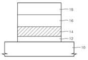
Translated fromKorean도 1은 종래의 전하트랩층을 포함하는 메모리소자를 나타내는 단면도이다.1 is a cross-sectional view illustrating a memory device including a conventional charge trap layer.
도 2a는 정공의 트랩밀도가 높은 실리콘 질화막(Si3N4)을 전하트랩층으로 사용한 경우의 에너지 밴드값의 상태를 나타낸 밴드 다이아그램(diagram)이다.FIG. 2A is a band diagram showing the state of energy band values when a silicon nitride film (Si3 N4 ) having high hole trap density is used as the charge trap layer.
도 2b는 본 발명의 사례인 SRN과 저압(low pressure; LP) SiN을 각각 전하트랩층으로 적용한 메모리소자의 게이트전압(VG)에 따른 드레인전류(ID)를 비교한 그래프이다.FIG. 2B is a graph comparing drain current ID according to gate voltage VG of a memory device in which SRN and low pressure (LP) SiN, which is an example of the present invention, are respectively applied as a charge trap layer.
도 3a는 전자의 트랩밀도가 높은 알루미늄질화물(AlN)을 전하트랩층으로 사용한 경우의 에너지 밴드값의 상태를 나타낸 밴드 다이아그램(diagram)이다.3A is a band diagram showing the state of the energy band value when aluminum nitride (AlN) having a high trap density of electrons is used as the charge trap layer.
도 3b는 본 발명의 사례인 AlN의 프로그램 및 소거 관계를 전압(V)과 커패시턴스 밀도(fF/㎛2)로 나타낸 그래프이다.3B is a graph showing a program and erase relationship of AlN, which is an example of the present invention, in terms of voltage (V) and capacitance density (fF / μm2 ).
도 4a 내지 도 4c는 각각 제1 질화막과 제2 질화막이 순차적으로 적층된 제1 전하트랩층, 제2 질화막과 제1 질화막이 순차적으로 적층된 제2 전하트랩층 및 복수개의 제1 전하트랩층으로 이루어진 제3 전하트랩층이 적용된 메모리소자를 개념적으로 나타낸 단면도이다.4A to 4C illustrate a first charge trap layer in which a first nitride film and a second nitride film are sequentially stacked, a second charge trap layer in which a second nitride film and a first nitride film are sequentially stacked, and a plurality of first charge trap layers, respectively. A cross-sectional view conceptually illustrating a memory device to which a third charge trap layer is formed.
도 5a는 종래의 저압 SiN 전하트랩층을 적용한 메모리소자와 본 발명의 복합 전하트랩층(SRN 및 AlN 복합층)을 적용한 메모리소자의 프로그램에 대한 시간에 따른 문턱전압을 나타낸 그래프이다.5A is a graph illustrating a threshold voltage over time for a program of a memory device to which a conventional low voltage SiN charge trap layer is applied and a memory device to which the composite charge trap layer (SRN and AlN composite layer) of the present invention is applied.
도 5b는 종래의 저압 SiN 전하트랩층을 적용한 메모리소자와 본 발명의 복합 전하트랩층(SRN 및 AlN 복합층)을 적용한 메모리소자의 소거에 대한 시간에 따른 문턱전압을 나타낸 그래프이다.FIG. 5B is a graph illustrating a threshold voltage over time for erasing a memory device to which a conventional low voltage SiN charge trap layer is applied and a memory device to which a composite charge trap layer (SRN and AlN composite layer) of the present invention is applied.
도 6은 종래의 AlN 전하트랩층을 적용한 메모리소자와 본 발명의 복합 전하트랩층(SRN 및 AlN 복합층)을 적용한 메모리소자의 시간에 따른 문턱전압이 변화를 나타낸 그래프이다.FIG. 6 is a graph illustrating changes in threshold voltages of a memory device to which a conventional AlN charge trap layer is applied and a memory device to which a composite charge trap layer (SRN and AlN composite layer) of the present invention is applied.
*도면의 주요부분에 대한 부호의 설명** Description of the symbols for the main parts of the drawings *
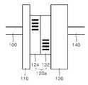
100; 기판 110; 터널 절연막100; A
120a, b, c: 복합 전하트랩층120a, b, c: composite charge trapping layer
130; 차단막 140; 게이트 전극130;
본 발명은 반도체 메모리소자에 관한 것으로, 특히 서로 다른 전하의 트랩밀도를 갖는 복수개의 유전체층이 적층된 전하트랩층을 포함하는 메모리소자에 관한 것이다.BACKGROUND OF THE INVENTION 1. Field of the Invention The present invention relates to a semiconductor memory device, and more particularly to a memory device including a charge trap layer in which a plurality of dielectric layers having different charge trap densities are stacked.
일반적으로, 전원의 공급이 중단되더라도 데이터가 유지되는 반도체 메모리소자 는 불휘발성 메모리소자라고 불리고 있다. 불휘발성 메모리소자는 데이터 저장능력이 뛰어나 이동통신 시스템, 메모리 카드 등에 폭넓게 채용되고 있다. 불휘발성 메모리소자는 전하트랩층에 전하를 저장하고 소거하는 방식을 이용하고 있다. 일반적인 전하트랩 메모리 소자는 단층(single layer)의 전하트랩층을 사용하고 있다.In general, a semiconductor memory device in which data is retained even when power supply is interrupted is called a nonvolatile memory device. Nonvolatile memory devices have excellent data storage capability and are widely used in mobile communication systems and memory cards. Nonvolatile memory devices use a method of storing and erasing charges in a charge trap layer. A typical charge trap memory device uses a single layer of charge trap layers.
도 1은 종래의 전하트랩층을 포함하는 메모리소자를 나타내는 단면도이다.1 is a cross-sectional view illustrating a memory device including a conventional charge trap layer.
도 1을 참조하면, 기판(10), 예컨대 실리콘 기판 상에 터널절연막(12), 전하트랩층(14), 차단막(16; blocking layer) 및 게이트전극(18)이 순차적으로 적층되어 있다. 전하(charge)는 터널절연막(12) 및 차단막(16)과 전하트랩층(14)의 에너지 밴드값의 차이에 의해 전하트랩층(14)에 트랩되고 유지(retention)된다. 이때, 단층의 전하트랩층(14)을 이용한 메모리소자인 단일레벨 셀(single level cell; SLC)는 하나의 셀(cell)에 하나의 정보만을 저장할 수 있다.Referring to FIG. 1, a
그런데, 단일레벨 셀에서 프로그램(program)과 소거(erase) 동작에서 확보할 수 있는 문턱전압(VTH, memory window라고도 함)은 전하트랩층(14)을 이루는 물질의 고유한 특성에 의해 제한적인 값을 가지게 된다. 단일레벨 셀의 경우, 하나의 전하트랩층으로 확보한 문턱전압으로도 소자의 동작이 충분하다. 한편, 고용량의 메모리소자를 만들기 위해, 하나의 셀에 복수 개의 정보를 저장하는 복수레벨 셀(multi level cell; MLC)이 대두되고 있다. 그런데, 복수레벨 셀의 동작을 보장하기 위해서는 문턱전압을 극대화하는 방법이 요구되고 있다. 또한 정보를 저장하고 읽어 들이는 프로그램 및 소거의 속도는 메모리소자의 용량이 커지기 때문에, 단일레벨 셀에 비해 커져야 한다. 하지만, 하나의 전하트랩층을 사용하면 프로그램과 소거 동작에서 문턱전압의 극대화와 속도 향상이라는 두 가지 조건을 만족시키기 어렵다.However, in a single-level cell, the threshold voltage (also referred to as a memory window, VTH ) that can be secured during program and erase operations is limited by the inherent properties of the material forming the
따라서, 본 발명이 이루고자 하는 기술적 과제는 프로그램과 소거 동작에서 문턱전압의 극대화와 속도의 향상을 가져오는 전하트랩층을 포함하는 메모리소자를 제공하는 데 있다.Accordingly, an aspect of the present invention is to provide a memory device including a charge trap layer that maximizes a threshold voltage and improves speed in program and erase operations.
상기 기술적 과제를 달성하기 위한 본 발명에 의한 메모리소자는 반도체 기판과, 상기 반도체 기판 상에 배치된 터널절연막 및 상기 터널절연막 상에 배치되고, 정공(hole) 트랩 밀도가 높은 제1 질화막과 전자(electron) 트랩 밀도가 높은 제2 질화막의 적어도 하나 쌍으로 이루어진 전하트랩층을 포함한다. 상기 전하트랩층의 상부면을 덮는 차단막을 포함한다.In accordance with another aspect of the present invention, a memory device includes a semiconductor substrate, a tunnel insulating film disposed on the semiconductor substrate, a first nitride film disposed on the tunnel insulating film, and having a high hole trap density. electron) a charge trap layer composed of at least one pair of second nitride films having a high trap density. And a blocking film covering an upper surface of the charge trap layer.
본 발명에 있어서, 상기 제1 질화막과 상기 터널절연막과의 가전자대 에너지 밴드값의 차이(△Ev)가 2~3 eV이고, 상기 제2 질화막과 상기 터널절연막과의 가전자대 에너지 밴드값의 차이(△Ev)가 1~1.5 eV일 수 있다. 또한, 상기 제1 질화막과 상기 차단막과의 가전자대 에너지 밴드값의 차이(△Ev)가 2.5~3.5 eV이고, 상기 제2 질화막과 상기 차단막과의 가전자대 에너지 밴드값의 차이(△Ev)가 1~1.5 eV일 수 있다.In the present invention, the difference (ΔEv) of the valence band energy band value between the first nitride film and the tunnel insulation film is 2 to 3 eV, and the difference in the valence band energy band value between the second nitride film and the tunnel insulation film is different. (ΔEv) may be 1 to 1.5 eV. In addition, the difference (ΔEv) of the valence band energy band value between the first nitride film and the blocking film is 2.5 to 3.5 eV, and the difference (ΔEv) of the valence band energy band value between the second nitride film and the blocking film is It may be 1 to 1.5 eV.
상기 제1 질화막은 실리콘(Si)이 풍부한 질화물(Si rich nitride: SRN)으 로 이루어질 수 있고, 상기 제2 질화막은 알루미늄 질화물(AlN)으로 이루어질 수 있다.The first nitride layer may be made of Si rich nitride (SRN), and the second nitride layer may be made of aluminum nitride (AlN).
본 발명의 실시예는 정공의 트랩밀도(trap density)가 높은 질화막과 전자의 트랩밀도가 높은 질화막이 쌍을 이루는 전하트랩층을 포함하는 메모리소자를 제공할 것이다. 정공의 트랩밀도가 높은 질화막은 실리콘이 풍부한 질화물(Si rich nitride; SRN)을 사례로서 제시할 것이고, 전자의 트랩밀도가 높은 질화막은 AlN을 제시할 것이다. 이때, 정공 및 전자의 트랩밀도는 에너지 밴드값의 차이에 의해 결정된다.Embodiments of the present invention will provide a memory device including a charge trap layer in which a nitride film having a high trap density of holes and a nitride film having a high trap density of electrons are paired. A nitride film having a high trap density of holes will present Si rich nitride (SRN) as an example, and a nitride film having a high trap density of electrons will present AlN. At this time, the trap density of the hole and the electron is determined by the difference in the energy band value.
도 2a는 정공의 트랩밀도가 높은 실리콘 질화막(Si3N4)를 전하트랩층으로 사용한 경우의 에너지 밴드값의 상태를 나타낸 밴드 다이아그램(diagram)이다. 여기서, Si3N4는 본 발명의 사례인 SRN보다 실리콘의 함량이 적은 것이나, 본 발명의 특징 중의 하나인 정공의 트랩밀도가 높은 질화막을 설명하기 위하여 Si3N4이 전하트랩층으로 사용되는 경우를 살펴본 것이다.FIG. 2A is a band diagram showing a state of an energy band value when a silicon nitride film (Si3 N4 ) having a high hole trap density is used as a charge trap layer. Here, Si3 N4 has a lower silicon content than SRN, which is an example of the present invention, but Si3 N4 is used as a charge trap layer to explain a nitride film having a high hole trap density. We have seen the case.
도 2a를 참조하면, Si3N4를 전하트랩층으로 사용하는 메모리소자는 기판(100) 상에 터널절연막(110), 전하트랩층인 Si3N4막, 차단막(130) 및 게이트전극(140)이 순차적으로 적층되어 있다. 여기서, 기판(100)은 실리콘층, 터널절연막(110)은 실리콘산화물(SiO2)층, 차단막(130)은 알루미늄산화물(Al2O3)층 및 게이트전극(140)은 폴리실리콘층을 각각 사용하였다. 도시된 바와 같이, 실리콘산화물 층(110)과 Si3N4막과의 가전자대 에너지 밴드값의 차이(△Ev)는 2.85 eV이고, 전도대 에너지 밴드값의 차이(△Ec)는 1.05 eV이다. 즉, Si3N4막은 트랩된 정공을 유지(retention)하는 것이 전자를 유지하는 것보다 유리하다. 또한, 알루미늄 산화막(130)과 Si3N4막과의 가전자대 에너지 밴드값의 차이(△Ev)는 3.0 eV이고, 전도대 에너지 밴드값의 차이(△Ec)는 0.75 eV이다. 즉, Si3N4막은 전자보다는 정공의 트랩에 유리하다. 따라서, Si3N4막은 전자보다는 정공의 트랩밀도가 높은 전하트랩층으로 유용하다.Referring to FIG. 2A, a memory device using Si3 N4 as a charge trap layer includes a
본 발명에 적용될 수 있는 정공 트랩밀도가 높은 질화막(제1 질화막)은 터널절연막과의 가전자대 에너지 밴드값의 차이(△Ev)가 2~3 eV이고, 차단막과의 가전자대 에너지 밴드값의 차이(△Ev)가 2.5~3.5 eV인 것이 바람직하다.The nitride film (first nitride film) having a high hole trap density applicable to the present invention has a difference in valence band energy band value (ΔEv) of 2 to 3 eV from the tunnel insulation film and a difference in valence band energy band value from the blocking film. It is preferable that ((DELTA) Ev) is 2.5-3.5 eV.
도 2b는 본 발명의 사례인 SRN(△ 표시)과 저압 SiN(○ 표시; low pressure(LP)-SiN)을 각각 전하트랩층으로 적용한 메모리소자의 게이트전압(VG)에 따른 드레인전류(ID)를 비교한 그래프이다. 여기서, LP SiN을 비교하면, Si과 N의 함량(원자량)에 따른 VG와 ID의 관계를 알 수 있기 때문이다. 따라서, 상기 VG와 ID의 관계를 살펴봄으로써, Si과 N의 함량에 따른 전하트랩층로서의 특징을 비교할 수 있다. 이때, 프로그램은 17V의 VG에서 100 μsec 동안 진행하였고, 소거는 -19V에서 10msec 동안 실시하였다.2B illustrates a drain current I according to a gate voltage VG of a memory device in which SRN (Δ) and low pressure SiN (○ symbol; low pressure (LP) -SiN), which are examples of the present invention, are respectively applied as charge trap layers.It is a graph comparingD ). Here, comparing the LP SiN, it is because the relationship between VG and ID according to the content (atomic weight) of Si and N can be seen. Therefore, by looking at the relationship between the VG and ID , it is possible to compare the characteristics of the charge trap layer according to the content of Si and N. At this time, the program was conducted at 17V of the VG for 100 μsec, erasing was performed at -19V for 10msec.
도 2b를 참조하면, LP SiN에 의한 메모리소자의 프로그램과 소거가 일어나는 전압(이하, △VTH라고 함)은 a 만큼의 차이를 나타내었다. 이때, LP SiN의 Si과 N의 원자량 비는 1인 상태이다. 이에 반해, 본 발명에 적용되는 SRN이 적용된 메모리소자의 △VTH 는 b 만큼의 차이를 보였다. 다시 말해, SRN을 적용한 소자의 △VTH는LP SiN을 적용한 소자보다 현저하게 커진다는 것을 알 수 있다. 도시된 바와 같이, SRN층은 LP-SiN층보다 문턱전압이 음의 전압 쪽으로 이동하였다. △VTH가 커지면, 하나의 셀에 복수 개의 정보를 저장하는 복수레벨 셀(multi level cell; MLC)에 유용하게 적용될 수 있다.Referring to FIG. 2B, a voltage (hereinafter, referred to asΔV TH ) in which a program and erase of the memory device by LP SiN occurs (hereinafter, referred to asΔV TH ) is shown by a difference. At this time, the atomic weight ratio of Si and N in LP SiN is 1. In contrast, ΔVTH of the SRN-applied memory device according to the present invention showed a difference as much as b. In other words, ΔVTH of the device to which SRN is applied is It can be seen that it is significantly larger than the device to which LP SiN is applied. As shown, the SRN layer shifted the threshold voltage toward the negative voltage than the LP-SiN layer. When ΔVTH is increased, it may be usefully applied to a multi level cell (MLC) that stores a plurality of pieces of information in one cell.
본 발명에 있어서, 정공의 트랩밀도가 높은 실리콘질화막은 Si과 N의 원자량의 비가 1(SiN)보다 크고 2(Si2N) 이하인 것이 바람직하다. Si과 N과의 비를 2 이하로 한정한 것은, 단지 적절한 원자량의 비를 정한 것에 불과하다. 따라서, 정공의 트랩밀도가 높은 질화막이 실리콘질화막이 아닌 경우에는 상기 원자량의 비를 다르게 결정할 수도 있다. 즉, 정공의 트랩밀도가 높은 질화막으로 SRN을 제시하였으나, 정공의 트랩밀도가 높은 질화막은 앞서 설명한 밴드 다이아그램의 특징을 갖고 또한 가해지는 전압에 따라 △VTH 를 조절할 수 있는 물질이면 제한없이 가능하다. 다만, 여기서는 SRN을 사례로써 제시한 것이 불과하다.In the present invention, it is preferable that the silicon nitride film having a high trap density of holes has a ratio of atomic weight of Si and N greater than 1 (SiN) and less than or equal to 2 (Si2 N). The ratio of Si and N to 2 or less is merely a ratio of an appropriate atomic weight. Therefore, when the nitride film having a high hole trap density is not a silicon nitride film, the ratio of the atomic weight may be determined differently. That is, SRN is proposed as a nitride film having a high hole trap density, but a nitride film having a high hole trap density can be used as long as it has the characteristics of the band diagram described above and can controlΔV TH according to the applied voltage. Do. However, here is just an example of SRN.
도 3a는 전자의 트랩밀도가 높은 알루미늄질화물(AlN)을 전하트랩층으로 사용한 경우의 에너지 밴드값의 상태를 나타낸 밴드 다이아그램(diagram)이다.3A is a band diagram showing the state of the energy band value when aluminum nitride (AlN) having a high trap density of electrons is used as the charge trap layer.
도 3a를 참조하면, AlN을 전하트랩층으로 사용하는 메모리소자는 기판(100) 상에 터널절연막(110), 전하트랩층인 AlN층, 차단막(130) 및 게이트전극(140)이 순차적으로 적층되어 있다. 여기서, 기판(100)은 실리콘층, 터널절연막(110)은 실리콘산화물(SiO2)층, 차단막(130)은 알루미늄산화물(Al2O3)층 및 게이트전극(140)은 폴리실리콘층을 각각 사용하였다. 도시된 바와 같이, 실리콘산화물층(110)과 AlN층과의 가전자대 에너지 밴드값의 차이(△Ev)는 1.07 eV이고, 전도대 에너지 밴드값의 차이(△Ec)는 2.1 eV이다. 즉, AlN층은 트랩된 전자를 유지(retention)하는 것이 정공을 유지하는 것보다 유리하다. 또한, 알루미늄 산화막(130)과 AlN층과의 가전자대 에너지 밴드값의 차이(△Ev)는 1.12 eV이고, 전도대 에너지 밴드값의 차이(△Ec)는 1.8 eV이다. 즉, AlN 막은 정공보다 전자의 트랩에 유리하다. 따라서, AlN 막은 정공보다는 전자의 트랩밀도가 높은 전하트랩층으로 유용하다.Referring to FIG. 3A, in a memory device using AlN as a charge trap layer, a
본 발명에 적용될 수 있는 전자 트랩밀도가 높은 질화막(제2 질화막)은 터널절연막과의 가전자대 에너지 밴드값의 차이(△Ev)가 1~1.5 eV이고, 차단막과의 가전자대 에너지 밴드값의 차이(△Ev)가 1~1.5 eV인 것이 바람직하다.The nitride film (second nitride film) having a high electron trap density applicable to the present invention has a difference in valence band energy band value (ΔEv) from 1 to 1.5 eV with a tunnel insulating film and a difference in valence band energy band value from the blocking film. It is preferable that ((DELTA) Ev) is 1-1.5 eV.
도 3b는 AlN의 프로그램 및 소거 관계를 전압(V)와 커패시턴스 밀도(fF/㎛2)로 나타낸 그래프이다. 이때, 프로그램은 가해진 전압을 각각 11V(??), 12V(▽), 13V(△), 14V(○) 및 15V(□)로 변화시키면서 진행하였고, 소거는 각각 -11V(◆), -12V(▼), -13V(▲), -14V(●) 및 -15V(■)로 변화시키면서 실시하였다.3B is a graph showing the program and erase relationship of AlN in terms of voltage (V) and capacitance density (fF / μm 2). At this time, the program proceeded while changing the applied voltage to 11V (??), 12V (▽), 13V (△), 14V (○) and 15V (□), respectively, and the erase was -11V (◆), -12V respectively. (▼), -13V (▲), -14V (●), and -15V (■).
도 3b를 참조하면, AlN층을 전하트랩층으로 사용한 소자는 프로그램의 전압이 커짐에 따라 △VTH 가 커짐을 알 수 있다. 도시된 바와 같이, AlN층에 가해지는 전압에 따라 문턱전압은 양의 전압 쪽으로 이동하였다. △VTH가 커지면, 하나의 셀에 복수 개의 정보를 저장하는 복수레벨 셀(multi level cell; MLC)에 유용하게 적용될 수 있다. 이때, AlN은 육방정계(hexagonal) 구조를 가지는 것이 바람직하다.Referring to FIG. 3B, it can be seen that ΔVTH increases as the voltage of the program increases in the device using the AlN layer as the charge trap layer. As shown, the threshold voltage shifted toward the positive voltage according to the voltage applied to the AlN layer. When ΔVTH is increased, it may be usefully applied to a multi level cell (MLC) that stores a plurality of pieces of information in one cell. At this time, AlN preferably has a hexagonal structure (hexagonal) structure.
도 3a 및 도 3b에서, 전자의 트랩밀도가 높은 질화막으로 AlN을 제시하였으나, 전자의 트랩밀도가 높은 질화막은 앞서 설명한 에너지밴드 다이아그램의 특징을 갖고, 가해지는 전압에 따라 △VTH 를 조절할 수 있는 물질이면 제한없이 가능하다. 다만, 여기서는 AlN을 사례로써 제시한 것이 불과하다.In FIGS. 3A and 3B, AlN is provided as a nitride film having a high trap density of electrons, but a nitride film having a high trap density of electrons has the characteristics of the energy band diagram described above, and ΔVTH can be adjusted according to the applied voltage. As long as the substance is present, it is possible without limitation. However, here only AlN is presented as an example.
이하에서는 앞서 살펴본 정공의 트랩밀도가 높은 질화막(제1 질화막)과 전자의 트랩밀도가 높은 질화막(제2 질화막)을 적층하여 이루어진 전하트랩층(복합 전하층; hybrid trap layer)으로 사용하는 메모리소자에 대하여 설명하기로 한다.Hereinafter, a memory device used as a charge trap layer (hybrid trap layer) formed by stacking a nitride film having a high trap density of holes (first nitride film) and a nitride having a high trap density of electrons (second nitride film). This will be described.
도 4a 내지 도 4c는 본 발명의 메모리소자를 개념적으로 접근한 개략도이다. 구체적으로, 도 4a는 터널절연막(110)에 제1 질화막(122)과 제2 질화막(124)이 순차적으로 적층된 제1 전하트랩층(120a)이 적용된 것이고, 도 4b는 터널절연막(110)에 제2 질화막(124)과 제1 질화막(122)이 순차적으로 적층된 제2 전하트랩층(120b)이 적용된 것이며, 도 4c는 복수개의 제1 전하트랩층(120a)으로 이루어진 제3 전하트랩층(120c)이 적용된 것이다. 필요에 따라, 복수개의 제2 전하트랩 층(120b)이 적용될 수도 있을 것이다. 이때, 각 층(120a, 120b, 120c)을 달리 형성하는 이유는 필요에 따라 적절한 메모리소자의 특성을 확보하기 위한 것이다. 트랩된 전자 및 정공은 복수개의 짙은 사각형으로 표현되었다.4A to 4C are schematic views conceptually approaching the memory device of the present invention. In detail, FIG. 4A illustrates a first
도 4a 내지 도 4c를 참조하면, 기판(100), 예컨대 실리콘 기판 상에 터널절연막(110)으로 SiO2 층을 열산화법(thermal oxidation) 등에 의해 15 ~ 50Å 성장 시킨다. 그후, 복합 전하트랩층을 10-200Å 성장시킨다. 구체적으로, 제1 질화막(122)은 SRN 층을 LPCVD 혹은 ALD(atomic layer deposition) 방법으로 10 ~ 200Å을 성장시키며, 제2 질화막(124)은 AlN 층을 LPCVD 혹은 ALD 방법으로 10 ~ 200Å을 성장시킨다. 이어서, 차단막(130)인 SiO2, Al2O3, Hf2O, Si3N4 등의 고유전율 절연막(high-k dielectric)의 적어도 하나를 10~200Å 성장 시킨 후, 게이트 전극(140)을 형성하여 완성한다. 이때, 제1 질화막(122)과 제2 질화막(124)은 진공의 파괴없이 동일한 챔버 내에서 연속하여 형성할 수 있다.4A to 4C, the SiO2 layer is grown on the
한편, 도 4a와 같이, 제1 질화막(122)으로 SixNy층, 예컨대 SRN층과 차단막으로 Al2O3 사이에 제2 질화막(124)으로 AlN층을 삽입하면 다음과 같은 특성을 갖는다. SixNy층 상에 증착하는 Al2O3에 의해, SixNy층 상에는 원하지 않는 층, 예를 들어 SiON층이 형성된다. 원하지 않는 층은 터널절연막(110)에 인가되는 전기장을 감소시킨다. 그런데, SixNy층 상에 AlN층을 증착하면, 원하지 않는 층의 형성을 방지할 수 있다. 따라서, AlN 층에 의해, 터널절연막(110)에 인가되는 전기장을 원하는 값 으로 유지하여 프로그램 또는 소거에 대한 문턱전압의 변화를 안정화시킬 수 있다.On the other hand, as shown in Figure 4a, when the AlN layer is inserted into the
한편, 도 4b와 같이, 터널절연막(110)과 제1 질화막(122)으로 SixNy층, 예컨대 SRN층 사이에 제2 질화막(124)으로 AlN층을 삽입하면 다음과 같은 특성을 갖는다. 전하트랩물질인 제1 질화막(122)은 정공의 트랩밀도가 높으므로, 낮은 트랩이 존재한다. 낮은 트랩은 프로그램 후에 트랩된 전하가 하부의 터널절연막(110)을 통하여 기판(100)으로 빠져나는 원인이 될 수 있다. 전하가 빠져나가면, 전하를 유지하는 특성이 불량해진다. 그런데, 제2 질화막(124)으로 AlN을 터널절연막(110)과 제1 질화막(122)인 SixNy층 사이에 배치하면, 전하가 터널절연막(110)을 통하여 기판(100)으로 빠져나가는 것을 방지할 수 있다.On the other hand, as shown in FIG. 4B, when the AlN layer is inserted into the
한편, 본 발명의 메모리 소자를 구성하는 복합 전하트랩층의 폭이 종래의 SiN 단일층의 폭보다 2.5 ~ 3.5배 크더라도, 시간에 따른 문턱전압의 변화율은 동일한 패턴을 갖는다.
5a는 종래의 LP-SiN 전하트랩층을 적용한 메모리소자와 본 발명의 복합 전하트랩층(SRN 및 AlN 복합층)을 적용한 메모리소자의 프로그램에 대한 시간에 따른 문턱전압을 나타낸 그래프이다. 이때, 종래의 메모리소자에는 70Å 두께의 LP-SiN 전하트랩층을 사용하였고, 18V의 전압을 인가하였다(■). 본 발명의 메모리소자를 구성하는 복합 전하트랩층은 70Å의 SRN층 및 120Å의 AlN층으로 전체적으로 190Å이었다. 본 발명의 메모리소자는 인가전압을 16V(▼), 17V(●) 및 18V(▲)로 변화시키면서 측정하였다. 각각의 메모리소자는 전하트랩층을 제외하고 동일한 물질 및 구조, 즉 35Å 두께의 실리콘산화물(SiO2)의 터널절연막, 150Å 두께의 알루미늄산화막(Al2O3)의 차단막 및 TaN 게이트 전극으로 이루어진다.On the other hand, even if the width of the composite charge trap layer constituting the memory device of the present invention is 2.5 to 3.5 times larger than the width of the conventional SiN single layer, the rate of change of the threshold voltage over time has the same pattern.
5a is a graph showing a threshold voltage over time for a program of a memory device to which a conventional LP-SiN charge trap layer is applied and a memory device to which the composite charge trap layer (SRN and AlN composite layer) of the present invention is applied. In this case, a 70-kV LP-SiN charge trap layer was used as a conventional memory device, and a voltage of 18 V was applied (■). The composite charge trap layer constituting the memory device of the present invention was 190 kV in total, consisting of an SRN layer of 70 mV and an AlN layer of 120 mV. The memory device of the present invention was measured while varying the applied voltage to 16V (?), 17V (?), And 18V (▲). Each memory device is made of the same material and structure except for the charge trap layer, that is, a tunnel insulating film of 35 Å thick silicon oxide (SiO2 ), a blocking film of 150 Å thick aluminum oxide film (Al2 O3 ), and a TaN gate electrode.
도 5a에 의하면, 본 발명의 메모리소자에 17V를 100 μs 동안 인가하면 문 턱전압(VTH)은 1.9V이었다. 또한, 본 발명의 메모리소자와 종래의 메모리소자의 시간에 따른 문턱전압의 변화율은 거의 유사하였다. 즉, 각각의 소자의 문턱전압의 변화율을 시간에 따라 동일한 패턴을 나타내었다. 그런데, 본 발명의 전하트랩층은 종래의 전하트랩층에 비해 120Å 정도가 두껍다. 만일, 본 발명의 전하트랩층을 종래의 전하트랩층과 동일한 두께로 사용한다면, 상기 변화율을 증가할 것이다. 따라서, 본 발명의 메모리소자는 종래의 메모리소자에 비해 프로그래밍 속도를 향상시킬 수 있다.Referring to FIG. 5A, when 17V is applied to the memory device of the present invention for 100 mu s, the threshold voltage VTH is 1.9V. In addition, the rate of change of the threshold voltage over time of the memory device and the conventional memory device of the present invention were almost similar. That is, the rate of change of the threshold voltage of each device showed the same pattern over time. By the way, the charge trap layer of the present invention is about 120 kHz thicker than the conventional charge trap layer. If the charge trap layer of the present invention is used at the same thickness as the conventional charge trap layer, the change rate will be increased. Therefore, the memory device of the present invention can improve the programming speed compared to the conventional memory device.
도 5b는 종래의 저압 SiN 전하트랩층을 적용한 메모리소자와 본 발명의 복합 전하트랩층(SRN 및 AlN 복합층)을 적용한 메모리소자의 소거에 대한 시간에 따른 문턱전압을 나타낸 그래프이다. 이때, 종래의 메모리소자에는 70Å 두께의 SiN 전하트랩층을 사용하였고, -19V의 전압을 인가하였다(■). 본 발명의 메모리소자를 구성하는 복합 전하트랩층은 70Å의 SRN층 및 120Å의 ALN층으로 전체적으로 190Å이었다. 본 발명의 메모리소자는 인가전압을 -17V(▼), -18V(●) 및 -19V(▲)로 변화시키면서 측정하였다. 각각의 메모리소자는 전하트랩층을 제외하고 동일한 물질 및 구조, 즉 실리콘산화물(SiO2)의 터널절연막은 35Å, 알루미늄산화막(Al2O3)의 차단막은 150Å 및 TaN 게이트 전극으로 이루어진다.FIG. 5B is a graph illustrating a threshold voltage over time for erasing a memory device to which a conventional low voltage SiN charge trap layer is applied and a memory device to which a composite charge trap layer (SRN and AlN composite layer) of the present invention is applied. In this case, a 70-nm-thick SiN charge trap layer was used as a conventional memory device, and a voltage of −19 V was applied (■). The composite charge trap layer constituting the memory device of the present invention was 190 kV in total, consisting of an SRN layer of 70 mV and an ALN layer of 120 mV. The memory device of the present invention was measured while varying the applied voltage to -17V (?), -18V (?), And -19V ()). Each memory device has the same material and structure except for the charge trap layer, that is, the tunnel insulating film of silicon oxide (SiO 2) is 35 kV, the blocking film of aluminum oxide (Al2 O3 ) is 150 kV and the TaN gate electrode.
도 5b에 의하면, 본 발명의 메모리소자에 -17V를 10ms 동안 인가하면 문턱전압(VTH)은 -3.1V이었다. 또한, 본 발명의 메모리소자와 종래의 메모리소자의 시간에 따른 문턱전압의 변화율은 거의 유사하였다. 즉, 각각의 소자의 문턱전압의 변 화율을 시간에 따라 동일한 패턴을 나타내었다. 그런데, 본 발명의 전하트랩층은 종래의 전하트랩층에 비해 120Å 정도가 두껍다. 만일, 본 발명의 전하트랩층을 종래의 전하트랩층과 동일한 두께로 사용한다면, 상기 변화율을 증가할 것이다. 따라서, 본 발명의 메모리소자는 종래의 메모리소자에 비해 소거 속도를 향상시킬 수 있다.Referring to FIG. 5B, when -17V is applied to the memory device of the present invention for 10 ms, the threshold voltage VTH is -3.1V. In addition, the rate of change of the threshold voltage over time of the memory device and the conventional memory device of the present invention were almost similar. That is, the change rate of the threshold voltage of each device shows the same pattern over time. By the way, the charge trap layer of the present invention is about 120 kHz thicker than the conventional charge trap layer. If the charge trap layer of the present invention is used at the same thickness as the conventional charge trap layer, the change rate will be increased. Therefore, the memory device of the present invention can improve the erase speed as compared with the conventional memory device.
도 6은 단층의 AlN을 전하트랩층으로 적용한 메모리소자와 본 발명의 복합 전하트랩층(SRN 및 AlN 복합층)을 적용한 메모리소자의 시간에 따른 문턱전압이 변화를 나타낸 그래프이다. 이때, 측정은 250℃에서 2시간 동안 베이크(bake) 후 85℃에서 실시하였다. 그래프에서 작은 점들이 포함된 사각형은 프로그래밍과 소거의 반복을 하지 않은 메모리소자의 경우이고, 빗금이 칠해진 사각형은 프로그래밍과 소거를 1,000회 반복한 메모리소자의 경우이다. FIG. 6 is a graph illustrating changes in threshold voltages over time of a memory device using a single layer of AlN as a charge trap layer and a memory device to which the composite charge trap layer (SRN and AlN composite layer) of the present invention is applied. At this time, the measurement was carried out at 85 ℃ after baking (bak) for 2 hours at 250 ℃. The rectangles with small dots in the graph represent memory devices that do not repeat programming and erasing, and the hatched rectangles represent memory devices that repeat programming and erasing 1,000 times.
도 6을 참조하면, 종래의 메모리소자는 반복하지 않은 경우는 약 1.2V 그리고 반복한 경우는 약 1.4V의 문턱전압의 변화를 나타내었다. 이에 반해, 본 발명의 메모리소자는 반복하지 않은 경우는 약 0.02V 그리고 1,000회 반복한 경우는 약 0.2V 만큼 문턱전압이 변화되었다. 이에 따라, 본 발명의 메모리소자는 종래에 비해 시간에 따라 문턱전압의 변화가 적어, 장시간 사용해도 안정된 특성을 보일 것이다.Referring to FIG. 6, the conventional memory device exhibits a change in threshold voltage of about 1.2V when not repeated and about 1.4V when repeated. In contrast, the threshold voltage of the memory device of the present invention was changed by about 0.02V when not repeated and about 0.2V when repeated 1,000 times. Accordingly, the memory device of the present invention has less variation in threshold voltage with time than in the related art, and thus shows stable characteristics even when used for a long time.
이하 첨부된 도면을 참조하면서 본 발명의 바람직한 실시예를 상세히 설명한다. 다음에서 설명되는 실시예는 여러 가지 다른 형태로 변형될 수 있으며, 본 발명의 범위가 아래에서 상술되는 실시예에 한정되는 것은 아니다. 본 발명의 실시 예들은 당분야에서 통상의 지식을 가진 자에게 본 발명을 보다 완전하게 설명하기 위하여 제공되는 것이다. 실시예 전체에 걸쳐서 동일한 참조부호는 동일한 구성요소를 나타낸다.Hereinafter, exemplary embodiments of the present invention will be described in detail with reference to the accompanying drawings. The embodiments described below may be modified in various other forms, and the scope of the present invention is not limited to the embodiments described below. Embodiments of the present invention are provided to more fully explain the present invention to those skilled in the art. Like reference numerals denote like elements throughout the embodiments.
이상, 본 발명은 바람직한 실시예를 들어 상세하게 설명하였으나, 본 발명은 상기 실시예에 한정되지 않으며, 본 발명의 기술적 사상의 범위내에서 당분야에서 통상의 지식을 가진 자에 의하여 여러 가지 변형이 가능하다.As mentioned above, although the present invention has been described in detail with reference to preferred embodiments, the present invention is not limited to the above embodiments, and various modifications may be made by those skilled in the art within the scope of the technical idea of the present invention. It is possible.
상술한 본 발명에 따른 전하트랩층을 포함한 반도체 메모리소자는 정공(hole) 트랩 밀도가 높은 제1 질화막과 전자 트랩 밀도가 높은 제2 질화막의 적어도 하나 쌍으로 이루어진 전하트랩층을 사용함으로써, 프로그램과 소거 동작에서 문턱전압의 극대화와 속도의 향상을 가져오는 전하트랩층을 포함하는 메모리소자를 제공할 수 있다. 또한, 본 발명의 메모리 소자는 소자의 동작을 위한 문턱전압의 폭을 확장시켜 하나의 셀에 복수개의 정보를 저장할 수 있는 복수레벨 셀에 유용하게 적용할 수 있다. 나아가, 제2 질화막에 의해, 전하가 기판으로 유출되는 것을 방지할 수 있고 원하지 않은 막이 형성되는 것을 방지할 수 있다.The semiconductor memory device including the charge trap layer according to the present invention described above uses a charge trap layer composed of at least one pair of a first nitride film having a high hole trap density and a second nitride film having a high electron trap density. A memory device including a charge trap layer that maximizes a threshold voltage and improves speed in an erase operation may be provided. In addition, the memory device of the present invention can be usefully applied to a multi-level cell that can store a plurality of information in one cell by extending the width of the threshold voltage for the operation of the device. Furthermore, by the second nitride film, it is possible to prevent the charge from flowing out to the substrate and to prevent the formation of an unwanted film.
Claims (16)
Translated fromKoreanPriority Applications (2)
| Application Number | Priority Date | Filing Date | Title |
|---|---|---|---|
| KR1020060104683AKR100825787B1 (en) | 2006-08-18 | 2006-10-26 | Semiconductor memory device including a charge trap layer |
| US11/782,858US20080042192A1 (en) | 2006-08-18 | 2007-07-25 | Semiconductor memory device including charge trap layer with stacked nitride layers |
Applications Claiming Priority (3)
| Application Number | Priority Date | Filing Date | Title |
|---|---|---|---|
| KR20060078108 | 2006-08-18 | ||
| KR1020060078108 | 2006-08-18 | ||
| KR1020060104683AKR100825787B1 (en) | 2006-08-18 | 2006-10-26 | Semiconductor memory device including a charge trap layer |
Publications (2)
| Publication Number | Publication Date |
|---|---|
| KR20080016398A KR20080016398A (en) | 2008-02-21 |
| KR100825787B1true KR100825787B1 (en) | 2008-04-29 |
Family
ID=39100573
Family Applications (1)
| Application Number | Title | Priority Date | Filing Date |
|---|---|---|---|
| KR1020060104683AExpired - Fee RelatedKR100825787B1 (en) | 2006-08-18 | 2006-10-26 | Semiconductor memory device including a charge trap layer |
Country Status (2)
| Country | Link |
|---|---|
| US (1) | US20080042192A1 (en) |
| KR (1) | KR100825787B1 (en) |
Cited By (2)
| Publication number | Priority date | Publication date | Assignee | Title |
|---|---|---|---|---|
| US8426907B2 (en) | 2008-11-18 | 2013-04-23 | Samsung Electronics Co., Ltd. | Nonvolatile memory devices including multiple charge trapping layers |
| US8431984B2 (en) | 2008-11-18 | 2013-04-30 | Samsung Electronics Co., Ltd. | Nonvolatile memory devices including deep and high density trapping layers |
Families Citing this family (304)
| Publication number | Priority date | Publication date | Assignee | Title |
|---|---|---|---|---|
| JP2009253259A (en)* | 2008-04-11 | 2009-10-29 | Toshiba Corp | Nonvolatile semiconductor memory device, and method of manufacturing the same |
| KR20100107089A (en)* | 2009-03-25 | 2010-10-05 | 삼성전자주식회사 | Storage device and data storage system including of the same |
| US9394608B2 (en) | 2009-04-06 | 2016-07-19 | Asm America, Inc. | Semiconductor processing reactor and components thereof |
| US8802201B2 (en) | 2009-08-14 | 2014-08-12 | Asm America, Inc. | Systems and methods for thin-film deposition of metal oxides using excited nitrogen-oxygen species |
| US20130023129A1 (en) | 2011-07-20 | 2013-01-24 | Asm America, Inc. | Pressure transmitter for a semiconductor processing environment |
| US9017481B1 (en) | 2011-10-28 | 2015-04-28 | Asm America, Inc. | Process feed management for semiconductor substrate processing |
| JP5646569B2 (en)* | 2012-09-26 | 2014-12-24 | 株式会社東芝 | Semiconductor device |
| US10714315B2 (en) | 2012-10-12 | 2020-07-14 | Asm Ip Holdings B.V. | Semiconductor reaction chamber showerhead |
| US20160376700A1 (en) | 2013-02-01 | 2016-12-29 | Asm Ip Holding B.V. | System for treatment of deposition reactor |
| US11015245B2 (en) | 2014-03-19 | 2021-05-25 | Asm Ip Holding B.V. | Gas-phase reactor and system having exhaust plenum and components thereof |
| US9252155B2 (en)* | 2014-06-20 | 2016-02-02 | Macronix International Co., Ltd. | Memory device and method for manufacturing the same |
| US10858737B2 (en) | 2014-07-28 | 2020-12-08 | Asm Ip Holding B.V. | Showerhead assembly and components thereof |
| US9890456B2 (en) | 2014-08-21 | 2018-02-13 | Asm Ip Holding B.V. | Method and system for in situ formation of gas-phase compounds |
| US10941490B2 (en) | 2014-10-07 | 2021-03-09 | Asm Ip Holding B.V. | Multiple temperature range susceptor, assembly, reactor and system including the susceptor, and methods of using the same |
| US10276355B2 (en) | 2015-03-12 | 2019-04-30 | Asm Ip Holding B.V. | Multi-zone reactor, system including the reactor, and method of using the same |
| US10458018B2 (en) | 2015-06-26 | 2019-10-29 | Asm Ip Holding B.V. | Structures including metal carbide material, devices including the structures, and methods of forming same |
| US10211308B2 (en) | 2015-10-21 | 2019-02-19 | Asm Ip Holding B.V. | NbMC layers |
| US11139308B2 (en) | 2015-12-29 | 2021-10-05 | Asm Ip Holding B.V. | Atomic layer deposition of III-V compounds to form V-NAND devices |
| US10529554B2 (en) | 2016-02-19 | 2020-01-07 | Asm Ip Holding B.V. | Method for forming silicon nitride film selectively on sidewalls or flat surfaces of trenches |
| US10343920B2 (en) | 2016-03-18 | 2019-07-09 | Asm Ip Holding B.V. | Aligned carbon nanotubes |
| US10190213B2 (en) | 2016-04-21 | 2019-01-29 | Asm Ip Holding B.V. | Deposition of metal borides |
| US10865475B2 (en) | 2016-04-21 | 2020-12-15 | Asm Ip Holding B.V. | Deposition of metal borides and silicides |
| US10367080B2 (en) | 2016-05-02 | 2019-07-30 | Asm Ip Holding B.V. | Method of forming a germanium oxynitride film |
| US11453943B2 (en) | 2016-05-25 | 2022-09-27 | Asm Ip Holding B.V. | Method for forming carbon-containing silicon/metal oxide or nitride film by ALD using silicon precursor and hydrocarbon precursor |
| US9859151B1 (en) | 2016-07-08 | 2018-01-02 | Asm Ip Holding B.V. | Selective film deposition method to form air gaps |
| US10612137B2 (en) | 2016-07-08 | 2020-04-07 | Asm Ip Holdings B.V. | Organic reactants for atomic layer deposition |
| KR102532607B1 (en) | 2016-07-28 | 2023-05-15 | 에이에스엠 아이피 홀딩 비.브이. | Substrate processing apparatus and method of operating the same |
| US9887082B1 (en) | 2016-07-28 | 2018-02-06 | Asm Ip Holding B.V. | Method and apparatus for filling a gap |
| US9812320B1 (en) | 2016-07-28 | 2017-11-07 | Asm Ip Holding B.V. | Method and apparatus for filling a gap |
| US10643826B2 (en) | 2016-10-26 | 2020-05-05 | Asm Ip Holdings B.V. | Methods for thermally calibrating reaction chambers |
| US11532757B2 (en)* | 2016-10-27 | 2022-12-20 | Asm Ip Holding B.V. | Deposition of charge trapping layers |
| US10714350B2 (en) | 2016-11-01 | 2020-07-14 | ASM IP Holdings, B.V. | Methods for forming a transition metal niobium nitride film on a substrate by atomic layer deposition and related semiconductor device structures |
| US10229833B2 (en) | 2016-11-01 | 2019-03-12 | Asm Ip Holding B.V. | Methods for forming a transition metal nitride film on a substrate by atomic layer deposition and related semiconductor device structures |
| KR102546317B1 (en) | 2016-11-15 | 2023-06-21 | 에이에스엠 아이피 홀딩 비.브이. | Gas supply unit and substrate processing apparatus including the same |
| KR102762543B1 (en) | 2016-12-14 | 2025-02-05 | 에이에스엠 아이피 홀딩 비.브이. | Substrate processing apparatus |
| US11581186B2 (en) | 2016-12-15 | 2023-02-14 | Asm Ip Holding B.V. | Sequential infiltration synthesis apparatus |
| US11447861B2 (en) | 2016-12-15 | 2022-09-20 | Asm Ip Holding B.V. | Sequential infiltration synthesis apparatus and a method of forming a patterned structure |
| KR102700194B1 (en) | 2016-12-19 | 2024-08-28 | 에이에스엠 아이피 홀딩 비.브이. | Substrate processing apparatus |
| US10269558B2 (en) | 2016-12-22 | 2019-04-23 | Asm Ip Holding B.V. | Method of forming a structure on a substrate |
| US10867788B2 (en) | 2016-12-28 | 2020-12-15 | Asm Ip Holding B.V. | Method of forming a structure on a substrate |
| US11390950B2 (en) | 2017-01-10 | 2022-07-19 | Asm Ip Holding B.V. | Reactor system and method to reduce residue buildup during a film deposition process |
| US10468261B2 (en) | 2017-02-15 | 2019-11-05 | Asm Ip Holding B.V. | Methods for forming a metallic film on a substrate by cyclical deposition and related semiconductor device structures |
| US10529563B2 (en) | 2017-03-29 | 2020-01-07 | Asm Ip Holdings B.V. | Method for forming doped metal oxide films on a substrate by cyclical deposition and related semiconductor device structures |
| KR102457289B1 (en) | 2017-04-25 | 2022-10-21 | 에이에스엠 아이피 홀딩 비.브이. | Method for depositing a thin film and manufacturing a semiconductor device |
| US10892156B2 (en) | 2017-05-08 | 2021-01-12 | Asm Ip Holding B.V. | Methods for forming a silicon nitride film on a substrate and related semiconductor device structures |
| US10770286B2 (en) | 2017-05-08 | 2020-09-08 | Asm Ip Holdings B.V. | Methods for selectively forming a silicon nitride film on a substrate and related semiconductor device structures |
| US10886123B2 (en) | 2017-06-02 | 2021-01-05 | Asm Ip Holding B.V. | Methods for forming low temperature semiconductor layers and related semiconductor device structures |
| US12040200B2 (en) | 2017-06-20 | 2024-07-16 | Asm Ip Holding B.V. | Semiconductor processing apparatus and methods for calibrating a semiconductor processing apparatus |
| US11306395B2 (en) | 2017-06-28 | 2022-04-19 | Asm Ip Holding B.V. | Methods for depositing a transition metal nitride film on a substrate by atomic layer deposition and related deposition apparatus |
| KR20190009245A (en) | 2017-07-18 | 2019-01-28 | 에이에스엠 아이피 홀딩 비.브이. | Methods for forming a semiconductor device structure and related semiconductor device structures |
| US11374112B2 (en) | 2017-07-19 | 2022-06-28 | Asm Ip Holding B.V. | Method for depositing a group IV semiconductor and related semiconductor device structures |
| US10541333B2 (en) | 2017-07-19 | 2020-01-21 | Asm Ip Holding B.V. | Method for depositing a group IV semiconductor and related semiconductor device structures |
| US11018002B2 (en) | 2017-07-19 | 2021-05-25 | Asm Ip Holding B.V. | Method for selectively depositing a Group IV semiconductor and related semiconductor device structures |
| US10590535B2 (en) | 2017-07-26 | 2020-03-17 | Asm Ip Holdings B.V. | Chemical treatment, deposition and/or infiltration apparatus and method for using the same |
| TWI815813B (en) | 2017-08-04 | 2023-09-21 | 荷蘭商Asm智慧財產控股公司 | Showerhead assembly for distributing a gas within a reaction chamber |
| US10770336B2 (en) | 2017-08-08 | 2020-09-08 | Asm Ip Holding B.V. | Substrate lift mechanism and reactor including same |
| US10692741B2 (en) | 2017-08-08 | 2020-06-23 | Asm Ip Holdings B.V. | Radiation shield |
| US11769682B2 (en) | 2017-08-09 | 2023-09-26 | Asm Ip Holding B.V. | Storage apparatus for storing cassettes for substrates and processing apparatus equipped therewith |
| US11139191B2 (en) | 2017-08-09 | 2021-10-05 | Asm Ip Holding B.V. | Storage apparatus for storing cassettes for substrates and processing apparatus equipped therewith |
| US11830730B2 (en) | 2017-08-29 | 2023-11-28 | Asm Ip Holding B.V. | Layer forming method and apparatus |
| US11056344B2 (en) | 2017-08-30 | 2021-07-06 | Asm Ip Holding B.V. | Layer forming method |
| KR102491945B1 (en) | 2017-08-30 | 2023-01-26 | 에이에스엠 아이피 홀딩 비.브이. | Substrate processing apparatus |
| US11295980B2 (en) | 2017-08-30 | 2022-04-05 | Asm Ip Holding B.V. | Methods for depositing a molybdenum metal film over a dielectric surface of a substrate by a cyclical deposition process and related semiconductor device structures |
| KR102401446B1 (en) | 2017-08-31 | 2022-05-24 | 에이에스엠 아이피 홀딩 비.브이. | Substrate processing apparatus |
| KR102630301B1 (en) | 2017-09-21 | 2024-01-29 | 에이에스엠 아이피 홀딩 비.브이. | Method of sequential infiltration synthesis treatment of infiltrateable material and structures and devices formed using same |
| US10844484B2 (en) | 2017-09-22 | 2020-11-24 | Asm Ip Holding B.V. | Apparatus for dispensing a vapor phase reactant to a reaction chamber and related methods |
| US10658205B2 (en) | 2017-09-28 | 2020-05-19 | Asm Ip Holdings B.V. | Chemical dispensing apparatus and methods for dispensing a chemical to a reaction chamber |
| US10403504B2 (en) | 2017-10-05 | 2019-09-03 | Asm Ip Holding B.V. | Method for selectively depositing a metallic film on a substrate |
| US10923344B2 (en) | 2017-10-30 | 2021-02-16 | Asm Ip Holding B.V. | Methods for forming a semiconductor structure and related semiconductor structures |
| KR102505240B1 (en) | 2017-11-09 | 2023-03-06 | 삼성전자주식회사 | Three dimensional semiconductor device |
| US10910262B2 (en) | 2017-11-16 | 2021-02-02 | Asm Ip Holding B.V. | Method of selectively depositing a capping layer structure on a semiconductor device structure |
| US11022879B2 (en) | 2017-11-24 | 2021-06-01 | Asm Ip Holding B.V. | Method of forming an enhanced unexposed photoresist layer |
| WO2019103613A1 (en) | 2017-11-27 | 2019-05-31 | Asm Ip Holding B.V. | A storage device for storing wafer cassettes for use with a batch furnace |
| CN111344522B (en) | 2017-11-27 | 2022-04-12 | 阿斯莫Ip控股公司 | Including clean mini-environment device |
| US10872771B2 (en) | 2018-01-16 | 2020-12-22 | Asm Ip Holding B. V. | Method for depositing a material film on a substrate within a reaction chamber by a cyclical deposition process and related device structures |
| KR102695659B1 (en) | 2018-01-19 | 2024-08-14 | 에이에스엠 아이피 홀딩 비.브이. | Method for depositing a gap filling layer by plasma assisted deposition |
| TWI799494B (en) | 2018-01-19 | 2023-04-21 | 荷蘭商Asm 智慧財產控股公司 | Deposition method |
| US11018047B2 (en) | 2018-01-25 | 2021-05-25 | Asm Ip Holding B.V. | Hybrid lift pin |
| USD880437S1 (en) | 2018-02-01 | 2020-04-07 | Asm Ip Holding B.V. | Gas supply plate for semiconductor manufacturing apparatus |
| US11081345B2 (en) | 2018-02-06 | 2021-08-03 | Asm Ip Holding B.V. | Method of post-deposition treatment for silicon oxide film |
| WO2019158960A1 (en) | 2018-02-14 | 2019-08-22 | Asm Ip Holding B.V. | A method for depositing a ruthenium-containing film on a substrate by a cyclical deposition process |
| US10896820B2 (en) | 2018-02-14 | 2021-01-19 | Asm Ip Holding B.V. | Method for depositing a ruthenium-containing film on a substrate by a cyclical deposition process |
| US10731249B2 (en) | 2018-02-15 | 2020-08-04 | Asm Ip Holding B.V. | Method of forming a transition metal containing film on a substrate by a cyclical deposition process, a method for supplying a transition metal halide compound to a reaction chamber, and related vapor deposition apparatus |
| KR102636427B1 (en) | 2018-02-20 | 2024-02-13 | 에이에스엠 아이피 홀딩 비.브이. | Substrate processing method and apparatus |
| US10975470B2 (en) | 2018-02-23 | 2021-04-13 | Asm Ip Holding B.V. | Apparatus for detecting or monitoring for a chemical precursor in a high temperature environment |
| US11473195B2 (en) | 2018-03-01 | 2022-10-18 | Asm Ip Holding B.V. | Semiconductor processing apparatus and a method for processing a substrate |
| US11629406B2 (en) | 2018-03-09 | 2023-04-18 | Asm Ip Holding B.V. | Semiconductor processing apparatus comprising one or more pyrometers for measuring a temperature of a substrate during transfer of the substrate |
| US11114283B2 (en) | 2018-03-16 | 2021-09-07 | Asm Ip Holding B.V. | Reactor, system including the reactor, and methods of manufacturing and using same |
| KR102646467B1 (en) | 2018-03-27 | 2024-03-11 | 에이에스엠 아이피 홀딩 비.브이. | Method of forming an electrode on a substrate and a semiconductor device structure including an electrode |
| US11088002B2 (en) | 2018-03-29 | 2021-08-10 | Asm Ip Holding B.V. | Substrate rack and a substrate processing system and method |
| US11230766B2 (en) | 2018-03-29 | 2022-01-25 | Asm Ip Holding B.V. | Substrate processing apparatus and method |
| KR102501472B1 (en) | 2018-03-30 | 2023-02-20 | 에이에스엠 아이피 홀딩 비.브이. | Substrate processing method |
| KR102600229B1 (en) | 2018-04-09 | 2023-11-10 | 에이에스엠 아이피 홀딩 비.브이. | Substrate supporting device, substrate processing apparatus including the same and substrate processing method |
| JP7114308B2 (en)* | 2018-04-12 | 2022-08-08 | キオクシア株式会社 | semiconductor storage device |
| US12025484B2 (en) | 2018-05-08 | 2024-07-02 | Asm Ip Holding B.V. | Thin film forming method |
| TWI811348B (en) | 2018-05-08 | 2023-08-11 | 荷蘭商Asm 智慧財產控股公司 | Methods for depositing an oxide film on a substrate by a cyclical deposition process and related device structures |
| US12272527B2 (en) | 2018-05-09 | 2025-04-08 | Asm Ip Holding B.V. | Apparatus for use with hydrogen radicals and method of using same |
| KR20190129718A (en) | 2018-05-11 | 2019-11-20 | 에이에스엠 아이피 홀딩 비.브이. | Methods for forming a doped metal carbide film on a substrate and related semiconductor device structures |
| KR102596988B1 (en) | 2018-05-28 | 2023-10-31 | 에이에스엠 아이피 홀딩 비.브이. | Method of processing a substrate and a device manufactured by the same |
| TWI840362B (en) | 2018-06-04 | 2024-05-01 | 荷蘭商Asm Ip私人控股有限公司 | Wafer handling chamber with moisture reduction |
| US11718913B2 (en) | 2018-06-04 | 2023-08-08 | Asm Ip Holding B.V. | Gas distribution system and reactor system including same |
| US11286562B2 (en) | 2018-06-08 | 2022-03-29 | Asm Ip Holding B.V. | Gas-phase chemical reactor and method of using same |
| US10797133B2 (en) | 2018-06-21 | 2020-10-06 | Asm Ip Holding B.V. | Method for depositing a phosphorus doped silicon arsenide film and related semiconductor device structures |
| KR102568797B1 (en) | 2018-06-21 | 2023-08-21 | 에이에스엠 아이피 홀딩 비.브이. | Substrate processing system |
| KR102854019B1 (en) | 2018-06-27 | 2025-09-02 | 에이에스엠 아이피 홀딩 비.브이. | Periodic deposition method for forming a metal-containing material and films and structures comprising the metal-containing material |
| TWI873894B (en) | 2018-06-27 | 2025-02-21 | 荷蘭商Asm Ip私人控股有限公司 | Cyclic deposition methods for forming metal-containing material and films and structures including the metal-containing material |
| US10612136B2 (en) | 2018-06-29 | 2020-04-07 | ASM IP Holding, B.V. | Temperature-controlled flange and reactor system including same |
| KR102686758B1 (en) | 2018-06-29 | 2024-07-18 | 에이에스엠 아이피 홀딩 비.브이. | Method for depositing a thin film and manufacturing a semiconductor device |
| US10388513B1 (en) | 2018-07-03 | 2019-08-20 | Asm Ip Holding B.V. | Method for depositing silicon-free carbon-containing film as gap-fill layer by pulse plasma-assisted deposition |
| US10755922B2 (en) | 2018-07-03 | 2020-08-25 | Asm Ip Holding B.V. | Method for depositing silicon-free carbon-containing film as gap-fill layer by pulse plasma-assisted deposition |
| US10767789B2 (en) | 2018-07-16 | 2020-09-08 | Asm Ip Holding B.V. | Diaphragm valves, valve components, and methods for forming valve components |
| US11053591B2 (en) | 2018-08-06 | 2021-07-06 | Asm Ip Holding B.V. | Multi-port gas injection system and reactor system including same |
| US10883175B2 (en) | 2018-08-09 | 2021-01-05 | Asm Ip Holding B.V. | Vertical furnace for processing substrates and a liner for use therein |
| US10829852B2 (en) | 2018-08-16 | 2020-11-10 | Asm Ip Holding B.V. | Gas distribution device for a wafer processing apparatus |
| US11430674B2 (en) | 2018-08-22 | 2022-08-30 | Asm Ip Holding B.V. | Sensor array, apparatus for dispensing a vapor phase reactant to a reaction chamber and related methods |
| JP2020035128A (en)* | 2018-08-29 | 2020-03-05 | キオクシア株式会社 | Memory system |
| KR102707956B1 (en) | 2018-09-11 | 2024-09-19 | 에이에스엠 아이피 홀딩 비.브이. | Method for deposition of a thin film |
| US11024523B2 (en) | 2018-09-11 | 2021-06-01 | Asm Ip Holding B.V. | Substrate processing apparatus and method |
| US11049751B2 (en) | 2018-09-14 | 2021-06-29 | Asm Ip Holding B.V. | Cassette supply system to store and handle cassettes and processing apparatus equipped therewith |
| CN110970344B (en) | 2018-10-01 | 2024-10-25 | Asmip控股有限公司 | Substrate holding apparatus, system comprising the same and method of using the same |
| US11232963B2 (en) | 2018-10-03 | 2022-01-25 | Asm Ip Holding B.V. | Substrate processing apparatus and method |
| KR102592699B1 (en) | 2018-10-08 | 2023-10-23 | 에이에스엠 아이피 홀딩 비.브이. | Substrate support unit and apparatuses for depositing thin film and processing the substrate including the same |
| KR102546322B1 (en) | 2018-10-19 | 2023-06-21 | 에이에스엠 아이피 홀딩 비.브이. | Substrate processing apparatus and substrate processing method |
| KR102605121B1 (en) | 2018-10-19 | 2023-11-23 | 에이에스엠 아이피 홀딩 비.브이. | Substrate processing apparatus and substrate processing method |
| USD948463S1 (en) | 2018-10-24 | 2022-04-12 | Asm Ip Holding B.V. | Susceptor for semiconductor substrate supporting apparatus |
| US12378665B2 (en) | 2018-10-26 | 2025-08-05 | Asm Ip Holding B.V. | High temperature coatings for a preclean and etch apparatus and related methods |
| US11087997B2 (en) | 2018-10-31 | 2021-08-10 | Asm Ip Holding B.V. | Substrate processing apparatus for processing substrates |
| KR102748291B1 (en) | 2018-11-02 | 2024-12-31 | 에이에스엠 아이피 홀딩 비.브이. | Substrate support unit and substrate processing apparatus including the same |
| US11572620B2 (en) | 2018-11-06 | 2023-02-07 | Asm Ip Holding B.V. | Methods for selectively depositing an amorphous silicon film on a substrate |
| US11031242B2 (en) | 2018-11-07 | 2021-06-08 | Asm Ip Holding B.V. | Methods for depositing a boron doped silicon germanium film |
| US10818758B2 (en) | 2018-11-16 | 2020-10-27 | Asm Ip Holding B.V. | Methods for forming a metal silicate film on a substrate in a reaction chamber and related semiconductor device structures |
| US10847366B2 (en) | 2018-11-16 | 2020-11-24 | Asm Ip Holding B.V. | Methods for depositing a transition metal chalcogenide film on a substrate by a cyclical deposition process |
| US12040199B2 (en) | 2018-11-28 | 2024-07-16 | Asm Ip Holding B.V. | Substrate processing apparatus for processing substrates |
| US11217444B2 (en) | 2018-11-30 | 2022-01-04 | Asm Ip Holding B.V. | Method for forming an ultraviolet radiation responsive metal oxide-containing film |
| KR102636428B1 (en) | 2018-12-04 | 2024-02-13 | 에이에스엠 아이피 홀딩 비.브이. | A method for cleaning a substrate processing apparatus |
| US11158513B2 (en) | 2018-12-13 | 2021-10-26 | Asm Ip Holding B.V. | Methods for forming a rhenium-containing film on a substrate by a cyclical deposition process and related semiconductor device structures |
| TWI874340B (en) | 2018-12-14 | 2025-03-01 | 荷蘭商Asm Ip私人控股有限公司 | Method of forming device structure, structure formed by the method and system for performing the method |
| TWI866480B (en) | 2019-01-17 | 2024-12-11 | 荷蘭商Asm Ip 私人控股有限公司 | Methods of forming a transition metal containing film on a substrate by a cyclical deposition process |
| KR102727227B1 (en) | 2019-01-22 | 2024-11-07 | 에이에스엠 아이피 홀딩 비.브이. | Semiconductor processing device |
| CN111524788B (en) | 2019-02-01 | 2023-11-24 | Asm Ip私人控股有限公司 | Method for forming topologically selective films of silicon oxide |
| KR102626263B1 (en) | 2019-02-20 | 2024-01-16 | 에이에스엠 아이피 홀딩 비.브이. | Cyclical deposition method including treatment step and apparatus for same |
| TWI845607B (en) | 2019-02-20 | 2024-06-21 | 荷蘭商Asm Ip私人控股有限公司 | Cyclical deposition method and apparatus for filling a recess formed within a substrate surface |
| TWI873122B (en) | 2019-02-20 | 2025-02-21 | 荷蘭商Asm Ip私人控股有限公司 | Method of filling a recess formed within a surface of a substrate, semiconductor structure formed according to the method, and semiconductor processing apparatus |
| TWI838458B (en) | 2019-02-20 | 2024-04-11 | 荷蘭商Asm Ip私人控股有限公司 | Apparatus and methods for plug fill deposition in 3-d nand applications |
| TWI842826B (en) | 2019-02-22 | 2024-05-21 | 荷蘭商Asm Ip私人控股有限公司 | Substrate processing apparatus and method for processing substrate |
| KR102782593B1 (en) | 2019-03-08 | 2025-03-14 | 에이에스엠 아이피 홀딩 비.브이. | Structure Including SiOC Layer and Method of Forming Same |
| US11742198B2 (en) | 2019-03-08 | 2023-08-29 | Asm Ip Holding B.V. | Structure including SiOCN layer and method of forming same |
| KR102858005B1 (en) | 2019-03-08 | 2025-09-09 | 에이에스엠 아이피 홀딩 비.브이. | Method for Selective Deposition of Silicon Nitride Layer and Structure Including Selectively-Deposited Silicon Nitride Layer |
| JP2020167398A (en) | 2019-03-28 | 2020-10-08 | エーエスエム・アイピー・ホールディング・ベー・フェー | Door openers and substrate processing equipment provided with door openers |
| KR102809999B1 (en) | 2019-04-01 | 2025-05-19 | 에이에스엠 아이피 홀딩 비.브이. | Method of manufacturing semiconductor device |
| KR20200123380A (en) | 2019-04-19 | 2020-10-29 | 에이에스엠 아이피 홀딩 비.브이. | Layer forming method and apparatus |
| KR20200125453A (en) | 2019-04-24 | 2020-11-04 | 에이에스엠 아이피 홀딩 비.브이. | Gas-phase reactor system and method of using same |
| US11289326B2 (en) | 2019-05-07 | 2022-03-29 | Asm Ip Holding B.V. | Method for reforming amorphous carbon polymer film |
| KR20200130121A (en) | 2019-05-07 | 2020-11-18 | 에이에스엠 아이피 홀딩 비.브이. | Chemical source vessel with dip tube |
| KR20200130652A (en) | 2019-05-10 | 2020-11-19 | 에이에스엠 아이피 홀딩 비.브이. | Method of depositing material onto a surface and structure formed according to the method |
| JP7598201B2 (en) | 2019-05-16 | 2024-12-11 | エーエスエム・アイピー・ホールディング・ベー・フェー | Wafer boat handling apparatus, vertical batch furnace and method |
| JP7612342B2 (en) | 2019-05-16 | 2025-01-14 | エーエスエム・アイピー・ホールディング・ベー・フェー | Wafer boat handling apparatus, vertical batch furnace and method |
| USD975665S1 (en) | 2019-05-17 | 2023-01-17 | Asm Ip Holding B.V. | Susceptor shaft |
| USD947913S1 (en) | 2019-05-17 | 2022-04-05 | Asm Ip Holding B.V. | Susceptor shaft |
| USD935572S1 (en) | 2019-05-24 | 2021-11-09 | Asm Ip Holding B.V. | Gas channel plate |
| USD922229S1 (en) | 2019-06-05 | 2021-06-15 | Asm Ip Holding B.V. | Device for controlling a temperature of a gas supply unit |
| KR20200141002A (en) | 2019-06-06 | 2020-12-17 | 에이에스엠 아이피 홀딩 비.브이. | Method of using a gas-phase reactor system including analyzing exhausted gas |
| KR20200141931A (en) | 2019-06-10 | 2020-12-21 | 에이에스엠 아이피 홀딩 비.브이. | Method for cleaning quartz epitaxial chambers |
| KR20200143254A (en) | 2019-06-11 | 2020-12-23 | 에이에스엠 아이피 홀딩 비.브이. | Method of forming an electronic structure using an reforming gas, system for performing the method, and structure formed using the method |
| USD944946S1 (en) | 2019-06-14 | 2022-03-01 | Asm Ip Holding B.V. | Shower plate |
| USD931978S1 (en) | 2019-06-27 | 2021-09-28 | Asm Ip Holding B.V. | Showerhead vacuum transport |
| KR20210005515A (en) | 2019-07-03 | 2021-01-14 | 에이에스엠 아이피 홀딩 비.브이. | Temperature control assembly for substrate processing apparatus and method of using same |
| JP7499079B2 (en) | 2019-07-09 | 2024-06-13 | エーエスエム・アイピー・ホールディング・ベー・フェー | Plasma device using coaxial waveguide and substrate processing method |
| CN112216646A (en) | 2019-07-10 | 2021-01-12 | Asm Ip私人控股有限公司 | Substrate supporting assembly and substrate processing device comprising same |
| KR20210010307A (en) | 2019-07-16 | 2021-01-27 | 에이에스엠 아이피 홀딩 비.브이. | Substrate processing apparatus |
| KR102860110B1 (en) | 2019-07-17 | 2025-09-16 | 에이에스엠 아이피 홀딩 비.브이. | Methods of forming silicon germanium structures |
| KR20210010816A (en) | 2019-07-17 | 2021-01-28 | 에이에스엠 아이피 홀딩 비.브이. | Radical assist ignition plasma system and method |
| US11643724B2 (en) | 2019-07-18 | 2023-05-09 | Asm Ip Holding B.V. | Method of forming structures using a neutral beam |
| TWI839544B (en) | 2019-07-19 | 2024-04-21 | 荷蘭商Asm Ip私人控股有限公司 | Method of forming topology-controlled amorphous carbon polymer film |
| KR20210010817A (en) | 2019-07-19 | 2021-01-28 | 에이에스엠 아이피 홀딩 비.브이. | Method of Forming Topology-Controlled Amorphous Carbon Polymer Film |
| TWI851767B (en) | 2019-07-29 | 2024-08-11 | 荷蘭商Asm Ip私人控股有限公司 | Methods for selective deposition utilizing n-type dopants and/or alternative dopants to achieve high dopant incorporation |
| US12169361B2 (en) | 2019-07-30 | 2024-12-17 | Asm Ip Holding B.V. | Substrate processing apparatus and method |
| CN112309900A (en) | 2019-07-30 | 2021-02-02 | Asm Ip私人控股有限公司 | Substrate processing apparatus |
| CN112309899A (en) | 2019-07-30 | 2021-02-02 | Asm Ip私人控股有限公司 | Substrate processing apparatus |
| US11587815B2 (en) | 2019-07-31 | 2023-02-21 | Asm Ip Holding B.V. | Vertical batch furnace assembly |
| US11227782B2 (en) | 2019-07-31 | 2022-01-18 | Asm Ip Holding B.V. | Vertical batch furnace assembly |
| US11587814B2 (en) | 2019-07-31 | 2023-02-21 | Asm Ip Holding B.V. | Vertical batch furnace assembly |
| CN112323048B (en) | 2019-08-05 | 2024-02-09 | Asm Ip私人控股有限公司 | Liquid level sensor for chemical source container |
| CN112342526A (en) | 2019-08-09 | 2021-02-09 | Asm Ip私人控股有限公司 | Heater assembly including cooling device and method of using same |
| USD965524S1 (en) | 2019-08-19 | 2022-10-04 | Asm Ip Holding B.V. | Susceptor support |
| USD965044S1 (en) | 2019-08-19 | 2022-09-27 | Asm Ip Holding B.V. | Susceptor shaft |
| JP2021031769A (en) | 2019-08-21 | 2021-03-01 | エーエスエム アイピー ホールディング ビー.ブイ. | Production apparatus of mixed gas of film deposition raw material and film deposition apparatus |
| USD930782S1 (en) | 2019-08-22 | 2021-09-14 | Asm Ip Holding B.V. | Gas distributor |
| USD949319S1 (en) | 2019-08-22 | 2022-04-19 | Asm Ip Holding B.V. | Exhaust duct |
| KR20210024423A (en) | 2019-08-22 | 2021-03-05 | 에이에스엠 아이피 홀딩 비.브이. | Method for forming a structure with a hole |
| USD979506S1 (en) | 2019-08-22 | 2023-02-28 | Asm Ip Holding B.V. | Insulator |
| USD940837S1 (en) | 2019-08-22 | 2022-01-11 | Asm Ip Holding B.V. | Electrode |
| US11286558B2 (en) | 2019-08-23 | 2022-03-29 | Asm Ip Holding B.V. | Methods for depositing a molybdenum nitride film on a surface of a substrate by a cyclical deposition process and related semiconductor device structures including a molybdenum nitride film |
| KR20210024420A (en) | 2019-08-23 | 2021-03-05 | 에이에스엠 아이피 홀딩 비.브이. | Method for depositing silicon oxide film having improved quality by peald using bis(diethylamino)silane |
| KR102806450B1 (en) | 2019-09-04 | 2025-05-12 | 에이에스엠 아이피 홀딩 비.브이. | Methods for selective deposition using a sacrificial capping layer |
| KR102733104B1 (en) | 2019-09-05 | 2024-11-22 | 에이에스엠 아이피 홀딩 비.브이. | Substrate processing apparatus |
| US11562901B2 (en) | 2019-09-25 | 2023-01-24 | Asm Ip Holding B.V. | Substrate processing method |
| CN112593212B (en) | 2019-10-02 | 2023-12-22 | Asm Ip私人控股有限公司 | Method for forming topologically selective silicon oxide film by cyclic plasma enhanced deposition process |
| KR20210042810A (en) | 2019-10-08 | 2021-04-20 | 에이에스엠 아이피 홀딩 비.브이. | Reactor system including a gas distribution assembly for use with activated species and method of using same |
| TWI846953B (en) | 2019-10-08 | 2024-07-01 | 荷蘭商Asm Ip私人控股有限公司 | Substrate processing device |
| TW202128273A (en) | 2019-10-08 | 2021-08-01 | 荷蘭商Asm Ip私人控股有限公司 | Gas injection system, reactor system, and method of depositing material on surface of substratewithin reaction chamber |
| TWI846966B (en) | 2019-10-10 | 2024-07-01 | 荷蘭商Asm Ip私人控股有限公司 | Method of forming a photoresist underlayer and structure including same |
| US12009241B2 (en) | 2019-10-14 | 2024-06-11 | Asm Ip Holding B.V. | Vertical batch furnace assembly with detector to detect cassette |
| TWI834919B (en) | 2019-10-16 | 2024-03-11 | 荷蘭商Asm Ip私人控股有限公司 | Method of topology-selective film formation of silicon oxide |
| US11637014B2 (en) | 2019-10-17 | 2023-04-25 | Asm Ip Holding B.V. | Methods for selective deposition of doped semiconductor material |
| KR102845724B1 (en) | 2019-10-21 | 2025-08-13 | 에이에스엠 아이피 홀딩 비.브이. | Apparatus and methods for selectively etching films |
| KR20210050453A (en) | 2019-10-25 | 2021-05-07 | 에이에스엠 아이피 홀딩 비.브이. | Methods for filling a gap feature on a substrate surface and related semiconductor structures |
| US11646205B2 (en) | 2019-10-29 | 2023-05-09 | Asm Ip Holding B.V. | Methods of selectively forming n-type doped material on a surface, systems for selectively forming n-type doped material, and structures formed using same |
| KR20210054983A (en) | 2019-11-05 | 2021-05-14 | 에이에스엠 아이피 홀딩 비.브이. | Structures with doped semiconductor layers and methods and systems for forming same |
| US11501968B2 (en) | 2019-11-15 | 2022-11-15 | Asm Ip Holding B.V. | Method for providing a semiconductor device with silicon filled gaps |
| KR102861314B1 (en) | 2019-11-20 | 2025-09-17 | 에이에스엠 아이피 홀딩 비.브이. | Method of depositing carbon-containing material on a surface of a substrate, structure formed using the method, and system for forming the structure |
| US11450529B2 (en) | 2019-11-26 | 2022-09-20 | Asm Ip Holding B.V. | Methods for selectively forming a target film on a substrate comprising a first dielectric surface and a second metallic surface |
| CN112951697B (en) | 2019-11-26 | 2025-07-29 | Asmip私人控股有限公司 | Substrate processing apparatus |
| CN120432376A (en) | 2019-11-29 | 2025-08-05 | Asm Ip私人控股有限公司 | Substrate processing apparatus |
| CN112885692B (en) | 2019-11-29 | 2025-08-15 | Asmip私人控股有限公司 | Substrate processing apparatus |
| JP7527928B2 (en) | 2019-12-02 | 2024-08-05 | エーエスエム・アイピー・ホールディング・ベー・フェー | Substrate processing apparatus and substrate processing method |
| KR20210070898A (en) | 2019-12-04 | 2021-06-15 | 에이에스엠 아이피 홀딩 비.브이. | Substrate processing apparatus |
| KR20210078405A (en) | 2019-12-17 | 2021-06-28 | 에이에스엠 아이피 홀딩 비.브이. | Method of forming vanadium nitride layer and structure including the vanadium nitride layer |
| KR20210080214A (en) | 2019-12-19 | 2021-06-30 | 에이에스엠 아이피 홀딩 비.브이. | Methods for filling a gap feature on a substrate and related semiconductor structures |
| JP7636892B2 (en) | 2020-01-06 | 2025-02-27 | エーエスエム・アイピー・ホールディング・ベー・フェー | Channeled Lift Pins |
| JP7730637B2 (en) | 2020-01-06 | 2025-08-28 | エーエスエム・アイピー・ホールディング・ベー・フェー | Gas delivery assembly, components thereof, and reactor system including same |
| US11993847B2 (en) | 2020-01-08 | 2024-05-28 | Asm Ip Holding B.V. | Injector |
| KR20210093163A (en) | 2020-01-16 | 2021-07-27 | 에이에스엠 아이피 홀딩 비.브이. | Method of forming high aspect ratio features |
| KR102675856B1 (en) | 2020-01-20 | 2024-06-17 | 에이에스엠 아이피 홀딩 비.브이. | Method of forming thin film and method of modifying surface of thin film |
| TWI889744B (en) | 2020-01-29 | 2025-07-11 | 荷蘭商Asm Ip私人控股有限公司 | Contaminant trap system, and baffle plate stack |
| TW202513845A (en) | 2020-02-03 | 2025-04-01 | 荷蘭商Asm Ip私人控股有限公司 | Semiconductor structures and methods for forming the same |
| KR20210100010A (en) | 2020-02-04 | 2021-08-13 | 에이에스엠 아이피 홀딩 비.브이. | Method and apparatus for transmittance measurements of large articles |
| US11776846B2 (en) | 2020-02-07 | 2023-10-03 | Asm Ip Holding B.V. | Methods for depositing gap filling fluids and related systems and devices |
| KR20210103956A (en) | 2020-02-13 | 2021-08-24 | 에이에스엠 아이피 홀딩 비.브이. | Substrate processing apparatus including light receiving device and calibration method of light receiving device |
| TW202146691A (en) | 2020-02-13 | 2021-12-16 | 荷蘭商Asm Ip私人控股有限公司 | Gas distribution assembly, shower plate assembly, and method of adjusting conductance of gas to reaction chamber |
| TWI855223B (en) | 2020-02-17 | 2024-09-11 | 荷蘭商Asm Ip私人控股有限公司 | Method for growing phosphorous-doped silicon layer |
| CN113410160A (en) | 2020-02-28 | 2021-09-17 | Asm Ip私人控股有限公司 | System specially used for cleaning parts |
| KR20210113043A (en) | 2020-03-04 | 2021-09-15 | 에이에스엠 아이피 홀딩 비.브이. | Alignment fixture for a reactor system |
| US11876356B2 (en) | 2020-03-11 | 2024-01-16 | Asm Ip Holding B.V. | Lockout tagout assembly and system and method of using same |
| KR20210116240A (en) | 2020-03-11 | 2021-09-27 | 에이에스엠 아이피 홀딩 비.브이. | Substrate handling device with adjustable joints |
| KR102775390B1 (en) | 2020-03-12 | 2025-02-28 | 에이에스엠 아이피 홀딩 비.브이. | Method for Fabricating Layer Structure Having Target Topological Profile |
| US12173404B2 (en) | 2020-03-17 | 2024-12-24 | Asm Ip Holding B.V. | Method of depositing epitaxial material, structure formed using the method, and system for performing the method |
| KR102755229B1 (en) | 2020-04-02 | 2025-01-14 | 에이에스엠 아이피 홀딩 비.브이. | Thin film forming method |
| TWI887376B (en) | 2020-04-03 | 2025-06-21 | 荷蘭商Asm Ip私人控股有限公司 | Method for manufacturing semiconductor device |
| TWI888525B (en) | 2020-04-08 | 2025-07-01 | 荷蘭商Asm Ip私人控股有限公司 | Apparatus and methods for selectively etching silcon oxide films |
| US11821078B2 (en) | 2020-04-15 | 2023-11-21 | Asm Ip Holding B.V. | Method for forming precoat film and method for forming silicon-containing film |
| KR20210128343A (en) | 2020-04-15 | 2021-10-26 | 에이에스엠 아이피 홀딩 비.브이. | Method of forming chromium nitride layer and structure including the chromium nitride layer |
| US11996289B2 (en) | 2020-04-16 | 2024-05-28 | Asm Ip Holding B.V. | Methods of forming structures including silicon germanium and silicon layers, devices formed using the methods, and systems for performing the methods |
| KR20210130646A (en) | 2020-04-21 | 2021-11-01 | 에이에스엠 아이피 홀딩 비.브이. | Method for processing a substrate |
| CN113555279A (en) | 2020-04-24 | 2021-10-26 | Asm Ip私人控股有限公司 | Methods of forming vanadium nitride-containing layers and structures comprising the same |
| KR102866804B1 (en) | 2020-04-24 | 2025-09-30 | 에이에스엠 아이피 홀딩 비.브이. | Vertical batch furnace assembly comprising a cooling gas supply |
| TW202208671A (en) | 2020-04-24 | 2022-03-01 | 荷蘭商Asm Ip私人控股有限公司 | Methods of forming structures including vanadium boride and vanadium phosphide layers |
| KR20210132612A (en) | 2020-04-24 | 2021-11-04 | 에이에스엠 아이피 홀딩 비.브이. | Methods and apparatus for stabilizing vanadium compounds |
| KR20210132600A (en) | 2020-04-24 | 2021-11-04 | 에이에스엠 아이피 홀딩 비.브이. | Methods and systems for depositing a layer comprising vanadium, nitrogen, and a further element |
| KR102783898B1 (en) | 2020-04-29 | 2025-03-18 | 에이에스엠 아이피 홀딩 비.브이. | Solid source precursor vessel |
| KR20210134869A (en) | 2020-05-01 | 2021-11-11 | 에이에스엠 아이피 홀딩 비.브이. | Fast FOUP swapping with a FOUP handler |
| JP7726664B2 (en) | 2020-05-04 | 2025-08-20 | エーエスエム・アイピー・ホールディング・ベー・フェー | Substrate processing system for processing a substrate |
| KR102788543B1 (en) | 2020-05-13 | 2025-03-27 | 에이에스엠 아이피 홀딩 비.브이. | Laser alignment fixture for a reactor system |
| TW202146699A (en) | 2020-05-15 | 2021-12-16 | 荷蘭商Asm Ip私人控股有限公司 | Method of forming a silicon germanium layer, semiconductor structure, semiconductor device, method of forming a deposition layer, and deposition system |
| KR20210143653A (en) | 2020-05-19 | 2021-11-29 | 에이에스엠 아이피 홀딩 비.브이. | Substrate processing apparatus |
| KR20210145079A (en) | 2020-05-21 | 2021-12-01 | 에이에스엠 아이피 홀딩 비.브이. | Flange and apparatus for processing substrates |
| KR102795476B1 (en) | 2020-05-21 | 2025-04-11 | 에이에스엠 아이피 홀딩 비.브이. | Structures including multiple carbon layers and methods of forming and using same |
| TWI873343B (en) | 2020-05-22 | 2025-02-21 | 荷蘭商Asm Ip私人控股有限公司 | Reaction system for forming thin film on substrate |
| KR20210146802A (en) | 2020-05-26 | 2021-12-06 | 에이에스엠 아이피 홀딩 비.브이. | Method for depositing boron and gallium containing silicon germanium layers |
| TWI876048B (en) | 2020-05-29 | 2025-03-11 | 荷蘭商Asm Ip私人控股有限公司 | Substrate processing device |
| TW202212620A (en) | 2020-06-02 | 2022-04-01 | 荷蘭商Asm Ip私人控股有限公司 | Apparatus for processing substrate, method of forming film, and method of controlling apparatus for processing substrate |
| TW202208659A (en) | 2020-06-16 | 2022-03-01 | 荷蘭商Asm Ip私人控股有限公司 | Method for depositing boron containing silicon germanium layers |
| TW202218133A (en) | 2020-06-24 | 2022-05-01 | 荷蘭商Asm Ip私人控股有限公司 | Method for forming a layer provided with silicon |
| TWI873359B (en) | 2020-06-30 | 2025-02-21 | 荷蘭商Asm Ip私人控股有限公司 | Substrate processing method |
| US12431354B2 (en) | 2020-07-01 | 2025-09-30 | Asm Ip Holding B.V. | Silicon nitride and silicon oxide deposition methods using fluorine inhibitor |
| TW202202649A (en) | 2020-07-08 | 2022-01-16 | 荷蘭商Asm Ip私人控股有限公司 | Substrate processing method |
| KR20220010438A (en) | 2020-07-17 | 2022-01-25 | 에이에스엠 아이피 홀딩 비.브이. | Structures and methods for use in photolithography |
| KR20220011092A (en) | 2020-07-20 | 2022-01-27 | 에이에스엠 아이피 홀딩 비.브이. | Method and system for forming structures including transition metal layers |
| TWI878570B (en) | 2020-07-20 | 2025-04-01 | 荷蘭商Asm Ip私人控股有限公司 | Method and system for depositing molybdenum layers |
| US12322591B2 (en) | 2020-07-27 | 2025-06-03 | Asm Ip Holding B.V. | Thin film deposition process |
| KR20220021863A (en) | 2020-08-14 | 2022-02-22 | 에이에스엠 아이피 홀딩 비.브이. | Method for processing a substrate |
| US12040177B2 (en) | 2020-08-18 | 2024-07-16 | Asm Ip Holding B.V. | Methods for forming a laminate film by cyclical plasma-enhanced deposition processes |
| TW202228863A (en) | 2020-08-25 | 2022-08-01 | 荷蘭商Asm Ip私人控股有限公司 | Method for cleaning a substrate, method for selectively depositing, and reaction system |
| US11725280B2 (en) | 2020-08-26 | 2023-08-15 | Asm Ip Holding B.V. | Method for forming metal silicon oxide and metal silicon oxynitride layers |
| TW202229601A (en) | 2020-08-27 | 2022-08-01 | 荷蘭商Asm Ip私人控股有限公司 | Method of forming patterned structures, method of manipulating mechanical property, device structure, and substrate processing system |
| TW202217045A (en) | 2020-09-10 | 2022-05-01 | 荷蘭商Asm Ip私人控股有限公司 | Methods for depositing gap filing fluids and related systems and devices |
| USD990534S1 (en) | 2020-09-11 | 2023-06-27 | Asm Ip Holding B.V. | Weighted lift pin |
| KR20220036866A (en) | 2020-09-16 | 2022-03-23 | 에이에스엠 아이피 홀딩 비.브이. | Silicon oxide deposition method |
| USD1012873S1 (en) | 2020-09-24 | 2024-01-30 | Asm Ip Holding B.V. | Electrode for semiconductor processing apparatus |
| TWI889903B (en) | 2020-09-25 | 2025-07-11 | 荷蘭商Asm Ip私人控股有限公司 | Semiconductor processing method |
| US12009224B2 (en) | 2020-09-29 | 2024-06-11 | Asm Ip Holding B.V. | Apparatus and method for etching metal nitrides |
| KR20220045900A (en) | 2020-10-06 | 2022-04-13 | 에이에스엠 아이피 홀딩 비.브이. | Deposition method and an apparatus for depositing a silicon-containing material |
| CN114293174A (en) | 2020-10-07 | 2022-04-08 | Asm Ip私人控股有限公司 | Gas supply unit and substrate processing apparatus including the same |
| TW202229613A (en) | 2020-10-14 | 2022-08-01 | 荷蘭商Asm Ip私人控股有限公司 | Method of depositing material on stepped structure |
| TW202232565A (en) | 2020-10-15 | 2022-08-16 | 荷蘭商Asm Ip私人控股有限公司 | Method of manufacturing semiconductor device, and substrate treatment apparatus using ether-cat |
| TW202217037A (en) | 2020-10-22 | 2022-05-01 | 荷蘭商Asm Ip私人控股有限公司 | Method of depositing vanadium metal, structure, device and a deposition assembly |
| TW202223136A (en) | 2020-10-28 | 2022-06-16 | 荷蘭商Asm Ip私人控股有限公司 | Method for forming layer on substrate, and semiconductor processing system |
| TW202229620A (en) | 2020-11-12 | 2022-08-01 | 特文特大學 | Deposition system, method for controlling reaction condition, method for depositing |
| TW202229795A (en) | 2020-11-23 | 2022-08-01 | 荷蘭商Asm Ip私人控股有限公司 | A substrate processing apparatus with an injector |
| TW202235649A (en) | 2020-11-24 | 2022-09-16 | 荷蘭商Asm Ip私人控股有限公司 | Methods for filling a gap and related systems and devices |
| TW202235675A (en) | 2020-11-30 | 2022-09-16 | 荷蘭商Asm Ip私人控股有限公司 | Injector, and substrate processing apparatus |
| US12255053B2 (en) | 2020-12-10 | 2025-03-18 | Asm Ip Holding B.V. | Methods and systems for depositing a layer |
| TW202233884A (en) | 2020-12-14 | 2022-09-01 | 荷蘭商Asm Ip私人控股有限公司 | Method of forming structures for threshold voltage control |
| US11946137B2 (en) | 2020-12-16 | 2024-04-02 | Asm Ip Holding B.V. | Runout and wobble measurement fixtures |
| TW202232639A (en) | 2020-12-18 | 2022-08-16 | 荷蘭商Asm Ip私人控股有限公司 | Wafer processing apparatus with a rotatable table |
| TW202231903A (en) | 2020-12-22 | 2022-08-16 | 荷蘭商Asm Ip私人控股有限公司 | Transition metal deposition method, transition metal layer, and deposition assembly for depositing transition metal on substrate |
| TW202242184A (en) | 2020-12-22 | 2022-11-01 | 荷蘭商Asm Ip私人控股有限公司 | Precursor capsule, precursor vessel, vapor deposition assembly, and method of loading solid precursor into precursor vessel |
| TW202226899A (en) | 2020-12-22 | 2022-07-01 | 荷蘭商Asm Ip私人控股有限公司 | Plasma treatment device having matching box |
| USD980813S1 (en) | 2021-05-11 | 2023-03-14 | Asm Ip Holding B.V. | Gas flow control plate for substrate processing apparatus |
| USD1023959S1 (en) | 2021-05-11 | 2024-04-23 | Asm Ip Holding B.V. | Electrode for substrate processing apparatus |
| USD981973S1 (en) | 2021-05-11 | 2023-03-28 | Asm Ip Holding B.V. | Reactor wall for substrate processing apparatus |
| USD980814S1 (en) | 2021-05-11 | 2023-03-14 | Asm Ip Holding B.V. | Gas distributor for substrate processing apparatus |
| USD990441S1 (en) | 2021-09-07 | 2023-06-27 | Asm Ip Holding B.V. | Gas flow control plate |
| USD1060598S1 (en) | 2021-12-03 | 2025-02-04 | Asm Ip Holding B.V. | Split showerhead cover |
Citations (3)
| Publication number | Priority date | Publication date | Assignee | Title |
|---|---|---|---|---|
| JP2002009181A (en) | 2000-06-23 | 2002-01-11 | Sony Corp | Non-volatile semiconductor storage device and its manufacturing method |
| JP2002203917A (en) | 2000-10-26 | 2002-07-19 | Sony Corp | Nonvolatile semiconductor memory device and method of manufacturing the same |
| JP2005228760A (en) | 2004-02-10 | 2005-08-25 | Nippon Telegr & Teleph Corp <Ntt> | Charge storage memory and manufacturing method thereof |
Family Cites Families (9)
| Publication number | Priority date | Publication date | Assignee | Title |
|---|---|---|---|---|
| JPH0582795A (en)* | 1991-08-22 | 1993-04-02 | Rohm Co Ltd | Semiconductor memory device |
| US5640345A (en)* | 1993-10-01 | 1997-06-17 | Matsushita Electric Industrial Co., Ltd. | Semiconductor memory device and fabrication process |
| JP2005252069A (en)* | 2004-03-05 | 2005-09-15 | Tdk Corp | Electronic device and its manufacturing method |
| TWI244166B (en)* | 2004-03-11 | 2005-11-21 | Ememory Technology Inc | A non-volatile memory cell and fabricating method thereof |
| KR20050116976A (en)* | 2004-06-09 | 2005-12-14 | 동부아남반도체 주식회사 | Flash memory device and method for programming/erasing the same |
| US7612403B2 (en)* | 2005-05-17 | 2009-11-03 | Micron Technology, Inc. | Low power non-volatile memory and gate stack |
| US7402850B2 (en)* | 2005-06-21 | 2008-07-22 | Micron Technology, Inc. | Back-side trapped non-volatile memory device |
| US7429767B2 (en)* | 2005-09-01 | 2008-09-30 | Micron Technology, Inc. | High performance multi-level non-volatile memory device |
| US8809936B2 (en)* | 2006-07-31 | 2014-08-19 | Globalfoundries Inc. | Memory cell system with multiple nitride layers |
- 2006
- 2006-10-26KRKR1020060104683Apatent/KR100825787B1/ennot_activeExpired - Fee Related
- 2007
- 2007-07-25USUS11/782,858patent/US20080042192A1/ennot_activeAbandoned
Patent Citations (3)
| Publication number | Priority date | Publication date | Assignee | Title |
|---|---|---|---|---|
| JP2002009181A (en) | 2000-06-23 | 2002-01-11 | Sony Corp | Non-volatile semiconductor storage device and its manufacturing method |
| JP2002203917A (en) | 2000-10-26 | 2002-07-19 | Sony Corp | Nonvolatile semiconductor memory device and method of manufacturing the same |
| JP2005228760A (en) | 2004-02-10 | 2005-08-25 | Nippon Telegr & Teleph Corp <Ntt> | Charge storage memory and manufacturing method thereof |
Cited By (2)
| Publication number | Priority date | Publication date | Assignee | Title |
|---|---|---|---|---|
| US8426907B2 (en) | 2008-11-18 | 2013-04-23 | Samsung Electronics Co., Ltd. | Nonvolatile memory devices including multiple charge trapping layers |
| US8431984B2 (en) | 2008-11-18 | 2013-04-30 | Samsung Electronics Co., Ltd. | Nonvolatile memory devices including deep and high density trapping layers |
Also Published As
| Publication number | Publication date |
|---|---|
| US20080042192A1 (en) | 2008-02-21 |
| KR20080016398A (en) | 2008-02-21 |
Similar Documents
| Publication | Publication Date | Title |
|---|---|---|
| KR100825787B1 (en) | Semiconductor memory device including a charge trap layer | |
| US10727249B2 (en) | Memory cells, integrated structures and memory arrays | |
| US7402492B2 (en) | Method of manufacturing a memory device having improved erasing characteristics | |
| US6444545B1 (en) | Device structure for storing charge and method therefore | |
| US9214525B2 (en) | Gate stack having electron blocking layers on charge storage layers for electronic devices | |
| JP4907815B2 (en) | Manufacturing method of ONO floating gate electrode in 2-bit EEPROM device | |
| KR100843229B1 (en) | Flash memory device comprising a charge trap film of a hybrid structure and a manufacturing method thereof | |
| US20050199944A1 (en) | [non-volatile memory cell] | |
| TWI407492B (en) | Non-volatile nanocrystal memory and manufacturing method thereof | |
| US20090127611A1 (en) | Non-volatile memory device and memory card and system including the same | |
| KR101338166B1 (en) | A nonvolatile memory device and the method of the same | |
| US20050167734A1 (en) | Flash memory devices using large electron affinity material for charge trapping | |
| EP2166571B1 (en) | Memory device and its reading method | |
| KR100819003B1 (en) | Nonvolatile Memory Device Manufacturing Method | |
| WO2010087265A1 (en) | Nonvolatile semiconductor storage device and method for manufacturing same | |
| US7132337B2 (en) | Charge-trapping memory device and method of production | |
| US7394127B2 (en) | Non-volatile memory device having a charge storage oxide layer and operation thereof | |
| KR100905276B1 (en) | Flash memory device including multylayer tunnel insulator and method of fabricating the same | |
| CN1638130A (en) | Semiconductor memory and producing method thereof | |
| US20100259984A1 (en) | Erase method of nonvolatile semiconductor memory device | |
| US8542540B2 (en) | Nonvolatile memory and methods for manufacturing the same with molecule-engineered tunneling barriers | |
| KR100688586B1 (en) | Nonvolatile memory device having local charge trap layer and driving method thereof | |
| KR100763535B1 (en) | Manufacturing method of nonvolatile memory device | |
| KR101104090B1 (en) | Charge storage device and manufacturing method thereof | |
| KR20090003876A (en) | Flash memory device comprising a multilayer tunnel insulating film and method for manufacturing the same |
Legal Events
| Date | Code | Title | Description |
|---|---|---|---|
| A201 | Request for examination | ||
| PA0109 | Patent application | St.27 status event code:A-0-1-A10-A12-nap-PA0109 | |
| PA0201 | Request for examination | St.27 status event code:A-1-2-D10-D11-exm-PA0201 | |
| D13-X000 | Search requested | St.27 status event code:A-1-2-D10-D13-srh-X000 | |
| D14-X000 | Search report completed | St.27 status event code:A-1-2-D10-D14-srh-X000 | |
| E902 | Notification of reason for refusal | ||
| PE0902 | Notice of grounds for rejection | St.27 status event code:A-1-2-D10-D21-exm-PE0902 | |
| P11-X000 | Amendment of application requested | St.27 status event code:A-2-2-P10-P11-nap-X000 | |
| P13-X000 | Application amended | St.27 status event code:A-2-2-P10-P13-nap-X000 | |
| P11-X000 | Amendment of application requested | St.27 status event code:A-2-2-P10-P11-nap-X000 | |
| P13-X000 | Application amended | St.27 status event code:A-2-2-P10-P13-nap-X000 | |
| R15-X000 | Change to inventor requested | St.27 status event code:A-3-3-R10-R15-oth-X000 | |
| R16-X000 | Change to inventor recorded | St.27 status event code:A-3-3-R10-R16-oth-X000 | |
| PG1501 | Laying open of application | St.27 status event code:A-1-1-Q10-Q12-nap-PG1501 | |
| E701 | Decision to grant or registration of patent right | ||
| PE0701 | Decision of registration | St.27 status event code:A-1-2-D10-D22-exm-PE0701 | |
| GRNT | Written decision to grant | ||
| PR0701 | Registration of establishment | St.27 status event code:A-2-4-F10-F11-exm-PR0701 | |
| PR1002 | Payment of registration fee | St.27 status event code:A-2-2-U10-U11-oth-PR1002 Fee payment year number:1 | |
| PG1601 | Publication of registration | St.27 status event code:A-4-4-Q10-Q13-nap-PG1601 | |
| PR1001 | Payment of annual fee | St.27 status event code:A-4-4-U10-U11-oth-PR1001 Fee payment year number:4 | |
| FPAY | Annual fee payment | ||
| PR1001 | Payment of annual fee | St.27 status event code:A-4-4-U10-U11-oth-PR1001 Fee payment year number:5 | |
| R18-X000 | Changes to party contact information recorded | St.27 status event code:A-5-5-R10-R18-oth-X000 | |
| FPAY | Annual fee payment | ||
| PR1001 | Payment of annual fee | St.27 status event code:A-4-4-U10-U11-oth-PR1001 Fee payment year number:6 | |
| PR1001 | Payment of annual fee | St.27 status event code:A-4-4-U10-U11-oth-PR1001 Fee payment year number:7 | |
| PR1001 | Payment of annual fee | St.27 status event code:A-4-4-U10-U11-oth-PR1001 Fee payment year number:8 | |
| LAPS | Lapse due to unpaid annual fee | ||
| PC1903 | Unpaid annual fee | St.27 status event code:A-4-4-U10-U13-oth-PC1903 Not in force date:20160423 Payment event data comment text:Termination Category : DEFAULT_OF_REGISTRATION_FEE | |
| PC1903 | Unpaid annual fee | St.27 status event code:N-4-6-H10-H13-oth-PC1903 Ip right cessation event data comment text:Termination Category : DEFAULT_OF_REGISTRATION_FEE Not in force date:20160423 | |
| P22-X000 | Classification modified | St.27 status event code:A-4-4-P10-P22-nap-X000 | |
| P22-X000 | Classification modified | St.27 status event code:A-4-4-P10-P22-nap-X000 |