KR100819562B1 - Semiconductor device having retrograde area and manufacturing method thereof - Google Patents
Semiconductor device having retrograde area and manufacturing method thereofDownload PDFInfo
- Publication number
- KR100819562B1 KR100819562B1KR1020070004308AKR20070004308AKR100819562B1KR 100819562 B1KR100819562 B1KR 100819562B1KR 1020070004308 AKR1020070004308 AKR 1020070004308AKR 20070004308 AKR20070004308 AKR 20070004308AKR 100819562 B1KR100819562 B1KR 100819562B1
- Authority
- KR
- South Korea
- Prior art keywords
- region
- retrograde
- trench
- gate electrode
- impurity ions
- Prior art date
- Legal status (The legal status is an assumption and is not a legal conclusion. Google has not performed a legal analysis and makes no representation as to the accuracy of the status listed.)
- Expired - Fee Related
Links
Images


Classifications
- H—ELECTRICITY
- H01—ELECTRIC ELEMENTS
- H01L—SEMICONDUCTOR DEVICES NOT COVERED BY CLASS H10
- H01L21/00—Processes or apparatus adapted for the manufacture or treatment of semiconductor or solid state devices or of parts thereof
- H01L21/02—Manufacture or treatment of semiconductor devices or of parts thereof
- H01L21/04—Manufacture or treatment of semiconductor devices or of parts thereof the devices having potential barriers, e.g. a PN junction, depletion layer or carrier concentration layer
- H01L21/18—Manufacture or treatment of semiconductor devices or of parts thereof the devices having potential barriers, e.g. a PN junction, depletion layer or carrier concentration layer the devices having semiconductor bodies comprising elements of Group IV of the Periodic Table or AIIIBV compounds with or without impurities, e.g. doping materials
- H01L21/26—Bombardment with radiation
- H01L21/263—Bombardment with radiation with high-energy radiation
- H01L21/265—Bombardment with radiation with high-energy radiation producing ion implantation
- H01L21/26506—Bombardment with radiation with high-energy radiation producing ion implantation in group IV semiconductors
- H01L21/26513—Bombardment with radiation with high-energy radiation producing ion implantation in group IV semiconductors of electrically active species
- H01L21/2652—Through-implantation
- F—MECHANICAL ENGINEERING; LIGHTING; HEATING; WEAPONS; BLASTING
- F02—COMBUSTION ENGINES; HOT-GAS OR COMBUSTION-PRODUCT ENGINE PLANTS
- F02M—SUPPLYING COMBUSTION ENGINES IN GENERAL WITH COMBUSTIBLE MIXTURES OR CONSTITUENTS THEREOF
- F02M37/00—Apparatus or systems for feeding liquid fuel from storage containers to carburettors or fuel-injection apparatus; Arrangements for purifying liquid fuel specially adapted for, or arranged on, internal-combustion engines
- F02M37/22—Arrangements for purifying liquid fuel specially adapted for, or arranged on, internal-combustion engines, e.g. arrangements in the feeding system
- F—MECHANICAL ENGINEERING; LIGHTING; HEATING; WEAPONS; BLASTING
- F02—COMBUSTION ENGINES; HOT-GAS OR COMBUSTION-PRODUCT ENGINE PLANTS
- F02M—SUPPLYING COMBUSTION ENGINES IN GENERAL WITH COMBUSTIBLE MIXTURES OR CONSTITUENTS THEREOF
- F02M21/00—Apparatus for supplying engines with non-liquid fuels, e.g. gaseous fuels stored in liquid form
- F02M21/02—Apparatus for supplying engines with non-liquid fuels, e.g. gaseous fuels stored in liquid form for gaseous fuels
- F02M21/0203—Apparatus for supplying engines with non-liquid fuels, e.g. gaseous fuels stored in liquid form for gaseous fuels characterised by the type of gaseous fuel
- F02M21/0209—Hydrocarbon fuels, e.g. methane or acetylene
- F02M21/0212—Hydrocarbon fuels, e.g. methane or acetylene comprising at least 3 C-Atoms, e.g. liquefied petroleum gas [LPG], propane or butane
- H—ELECTRICITY
- H01—ELECTRIC ELEMENTS
- H01L—SEMICONDUCTOR DEVICES NOT COVERED BY CLASS H10
- H01L21/00—Processes or apparatus adapted for the manufacture or treatment of semiconductor or solid state devices or of parts thereof
- H01L21/02—Manufacture or treatment of semiconductor devices or of parts thereof
- H01L21/04—Manufacture or treatment of semiconductor devices or of parts thereof the devices having potential barriers, e.g. a PN junction, depletion layer or carrier concentration layer
- H01L21/18—Manufacture or treatment of semiconductor devices or of parts thereof the devices having potential barriers, e.g. a PN junction, depletion layer or carrier concentration layer the devices having semiconductor bodies comprising elements of Group IV of the Periodic Table or AIIIBV compounds with or without impurities, e.g. doping materials
- H01L21/26—Bombardment with radiation
- H01L21/263—Bombardment with radiation with high-energy radiation
- H01L21/265—Bombardment with radiation with high-energy radiation producing ion implantation
- H01L21/2658—Bombardment with radiation with high-energy radiation producing ion implantation of a molecular ion, e.g. decaborane
- H—ELECTRICITY
- H10—SEMICONDUCTOR DEVICES; ELECTRIC SOLID-STATE DEVICES NOT OTHERWISE PROVIDED FOR
- H10B—ELECTRONIC MEMORY DEVICES
- H10B12/00—Dynamic random access memory [DRAM] devices
- H10B12/01—Manufacture or treatment
- H10B12/02—Manufacture or treatment for one transistor one-capacitor [1T-1C] memory cells
- H10B12/05—Making the transistor
- H10B12/053—Making the transistor the transistor being at least partially in a trench in the substrate
- H—ELECTRICITY
- H10—SEMICONDUCTOR DEVICES; ELECTRIC SOLID-STATE DEVICES NOT OTHERWISE PROVIDED FOR
- H10D—INORGANIC ELECTRIC SEMICONDUCTOR DEVICES
- H10D62/00—Semiconductor bodies, or regions thereof, of devices having potential barriers
- H10D62/10—Shapes, relative sizes or dispositions of the regions of the semiconductor bodies; Shapes of the semiconductor bodies
- H10D62/17—Semiconductor regions connected to electrodes not carrying current to be rectified, amplified or switched, e.g. channel regions
- H10D62/213—Channel regions of field-effect devices
- H10D62/221—Channel regions of field-effect devices of FETs
- H10D62/235—Channel regions of field-effect devices of FETs of IGFETs
- H10D62/299—Channel regions of field-effect devices of FETs of IGFETs having lateral doping variations
- H—ELECTRICITY
- H10—SEMICONDUCTOR DEVICES; ELECTRIC SOLID-STATE DEVICES NOT OTHERWISE PROVIDED FOR
- H10D—INORGANIC ELECTRIC SEMICONDUCTOR DEVICES
- H10D64/00—Electrodes of devices having potential barriers
- H10D64/01—Manufacture or treatment
- H10D64/025—Manufacture or treatment forming recessed gates, e.g. by using local oxidation
- H10D64/027—Manufacture or treatment forming recessed gates, e.g. by using local oxidation by etching at gate locations
- H—ELECTRICITY
- H10—SEMICONDUCTOR DEVICES; ELECTRIC SOLID-STATE DEVICES NOT OTHERWISE PROVIDED FOR
- H10D—INORGANIC ELECTRIC SEMICONDUCTOR DEVICES
- H10D64/00—Electrodes of devices having potential barriers
- H10D64/20—Electrodes characterised by their shapes, relative sizes or dispositions
- H10D64/27—Electrodes not carrying the current to be rectified, amplified, oscillated or switched, e.g. gates
- H10D64/311—Gate electrodes for field-effect devices
- H10D64/411—Gate electrodes for field-effect devices for FETs
- H10D64/511—Gate electrodes for field-effect devices for FETs for IGFETs
- H10D64/517—Gate electrodes for field-effect devices for FETs for IGFETs characterised by the conducting layers
- H10D64/518—Gate electrodes for field-effect devices for FETs for IGFETs characterised by the conducting layers characterised by their lengths or sectional shapes
Landscapes
- Engineering & Computer Science (AREA)
- Physics & Mathematics (AREA)
- High Energy & Nuclear Physics (AREA)
- Manufacturing & Machinery (AREA)
- Microelectronics & Electronic Packaging (AREA)
- Condensed Matter Physics & Semiconductors (AREA)
- General Physics & Mathematics (AREA)
- Health & Medical Sciences (AREA)
- Computer Hardware Design (AREA)
- Toxicology (AREA)
- Power Engineering (AREA)
- Chemical & Material Sciences (AREA)
- Combustion & Propulsion (AREA)
- Spectroscopy & Molecular Physics (AREA)
- Mechanical Engineering (AREA)
- General Engineering & Computer Science (AREA)
- Chemical Kinetics & Catalysis (AREA)
- General Chemical & Material Sciences (AREA)
- Oil, Petroleum & Natural Gas (AREA)
- Semiconductor Memories (AREA)
- Insulated Gate Type Field-Effect Transistor (AREA)
Abstract
Translated fromKoreanDescription
Translated fromKorean도 1은 본 발명의 실시 예에 따른 레트로그레이드 영역을 갖는 반도체소자를 설명하기 위한 단면도이다.1 is a cross-sectional view for describing a semiconductor device having a retrograde region according to an exemplary embodiment of the inventive concept.
도 2 내지 도 9는 본 발명의 실시 예에 따른 레트로그레이드 영역을 갖는 반도체소자의 제조방법을 설명하기 위한 단면도들이다.2 to 9 are cross-sectional views illustrating a method of manufacturing a semiconductor device having a retrograde area according to an embodiment of the present invention.
도 10 및 도 11은 본 발명의 다른 실시 예들에 따른 레트로그레이드 영역을 갖는 반도체소자의 제조방법을 설명하기 위한 단면도들이다.10 and 11 are cross-sectional views illustrating a method of manufacturing a semiconductor device having a retrograde area according to other example embodiments of the inventive concepts.
본 발명은 반도체소자 및 그 제조방법에 관한 것으로, 특히 레트로그레이드 영역을 갖는 반도체소자 및 그 제조방법에 관한 것이다.The present invention relates to a semiconductor device and a method for manufacturing the same, and more particularly, to a semiconductor device having a retrograde region and a method for manufacturing the same.
반도체소자의 고집적화 필요에 따라 트랜지스터의 크기를 극한적으로 축소하려는 연구가 진행되고 있다. 상기 트랜지스터의 크기를 축소하기 위하여 게이트전 극의 평면 크기를 감소시키는 경우, 단 채널 효과(short channel effect)에 의한 오프 전류(off current) 증가 및 리프레시(refresh) 특성 저하와 같은 난관에 봉착하게 된다.As the need for high integration of semiconductor devices, research is being conducted to dramatically reduce the size of transistors. When the plane size of the gate electrode is reduced in order to reduce the size of the transistor, it encounters difficulties such as an increase in off current and a decrease in refresh characteristics due to a short channel effect. .
이러한 단 채널 효과의 극복을 위하여 상기 게이트전극의 평면 크기에 비하여 상대적으로 긴 유효 채널 길이를 갖는 리세스 채널 트랜지스터(recess channel transistor)가 제안된 바 있다.In order to overcome the short channel effect, a recess channel transistor having a relatively long effective channel length compared to the plane size of the gate electrode has been proposed.
상기 리세스 채널 트랜지스터는 반도체기판을 식각하여 형성된 게이트 트렌치 및 상기 게이트 트렌치를 채우는 게이트전극을 구비한다. 즉, 상기 게이트전극은 상기 반도체기판 내부로 신장된 구조를 갖는다. 상기 게이트전극에 문턱전압 이상의 게이트전압이 인가되면 상기 게이트전극의 하단표면에 대응하는 상기 반도체기판에 상기 리세스 채널 트랜지스터의 채널(channel)이 형성될 수 있다.The recess channel transistor includes a gate trench formed by etching a semiconductor substrate and a gate electrode filling the gate trench. That is, the gate electrode has a structure extending into the semiconductor substrate. When a gate voltage of at least a threshold voltage is applied to the gate electrode, a channel of the recess channel transistor may be formed on the semiconductor substrate corresponding to the bottom surface of the gate electrode.
이에 따라, 상기 리세스 채널 트랜지스터의 유효 채널 길이(effective channel length)는 상기 게이트 트렌치의 깊이에 비례하여 증가될 수 있다. 즉, 상기 게이트 트렌치를 깊게 형성하여 상기 리세스 채널 트랜지스터의 유효 채널 길이를 증가시킬 수 있다.Accordingly, an effective channel length of the recess channel transistor may be increased in proportion to the depth of the gate trench. That is, the gate trench may be deeply formed to increase the effective channel length of the recess channel transistor.
그런데 상기 게이트 트렌치의 깊이 증가는 바디 효과(body effect)에 의한 문턱전압의 상승을 가중시킨다. 일반적으로 상기 반도체기판은 접지되거나 바디 바이어스(body bias)가 인가된다. 상기 바디 바이어스는 트랜지스터의 문턱전압을 변화시킨다. 예를 들면, 상기 게이트전압이 양의 전압일 경우 상기 바디 바이어스는 음의 전압일 수 있다. 이 경우에, 상기 트랜지스터의 문턱전압은 상기 바디 바이어 스의 크기에 비례하여 상승될 수 있다.However, the increase in the depth of the gate trench increases the increase of the threshold voltage due to the body effect. In general, the semiconductor substrate is grounded or a body bias is applied. The body bias changes the threshold voltage of the transistor. For example, when the gate voltage is a positive voltage, the body bias may be a negative voltage. In this case, the threshold voltage of the transistor may be increased in proportion to the magnitude of the body bias.
여기서, 상기 게이트 트렌치의 깊이 증가는 상기 바디 바이어스에 의한 상기 문턱전압의 상승비율을 더욱 크게 할 수 있다. 상기 문턱전압의 상승은 낮은 동작전압을 갖는 반도체소자의 구현을 어렵게 한다.Here, increasing the depth of the gate trench may further increase the rate of increase of the threshold voltage due to the body bias. The increase in the threshold voltage makes it difficult to implement a semiconductor device having a low operating voltage.
한편, 채널영역에 레트로그레이드 영역을 갖는 반도체소자가 미국공개특허 제 US2003/0183856A1 호에 "채널영역에서 레트로그레이드 도펀트 프로필을 구비한 반도체소자 및 그 제조방법 (Semiconductor device having a retrograde dopant profile in a channel region and method for fabricating the same)" 이라는 제목으로 웨크조레크 등(Weiczorek et al.)에 의해 개시된 바 있다.On the other hand, a semiconductor device having a retrograde region in the channel region is disclosed in US Patent Publication No. US2003 / 0183856A1 "Semiconductor device having a retrograde dopant profile in a channel region and method for fabricating the same ”, as described by Weiczorek et al.
본 발명이 이루고자 하는 기술적 과제는 상술한 종래기술의 문제점을 개선하기 위한 것으로서, 유효 채널 길이를 증가시키면서 바디 바이어스(body bias)에 의한 문턱전압의 상승을 효율적으로 제어할 수 있는 반도체소자를 제공하는 데 있다.SUMMARY OF THE INVENTION The present invention has been made in an effort to improve the above-described problems of the related art, and provides a semiconductor device capable of efficiently controlling a rise in threshold voltage due to body bias while increasing an effective channel length. There is.
본 발명이 이루고자 하는 다른 기술적 과제는, 유효 채널 길이를 증가시키면서 바디 바이어스(body bias)에 의한 문턱전압의 상승을 효율적으로 제어할 수 있는 반도체소자의 형성방법을 제공하는 데 있다.Another object of the present invention is to provide a method of forming a semiconductor device capable of efficiently controlling the increase in the threshold voltage due to body bias while increasing the effective channel length.
상기 기술적 과제를 달성하기 위하여 본 발명은, 레트로그레이드 영역을 갖 는 반도체소자를 제공한다. 이 소자는 제 1 형 불순물 이온들을 갖는 반도체기판에 한정된 활성영역을 구비한다. 상기 활성영역은 레트로그레이드 영역(retrograde region), 상부 채널영역 및 서로 이격된 한 쌍의 소스/드레인 영역들을 갖는다. 상기 상부 채널영역은 상기 레트로그레이드 영역 상에 배치되고 상기 제 1 형 불순물 이온들을 구비한다. 상기 소스/드레인 영역들은 상기 상부 채널영역 상에 배치된다. 상기 레트로그레이드 영역은 제 2 형 불순물 이온들을 갖는다. 상기 활성영역에 형성된 게이트 트렌치를 채우는 게이트전극이 제공된다. 상기 게이트전극은 상기 소스/드레인 영역들 사이에 배치되고 상기 상부 채널영역을 관통하여 상기 레트로그레이드 영역 내에 신장된다.In order to achieve the above technical problem, the present invention provides a semiconductor device having a retrograde area. This device has an active region defined in a semiconductor substrate having first type impurity ions. The active region has a retrograde region, an upper channel region and a pair of source / drain regions spaced apart from each other. The upper channel region is disposed on the retrograde region and includes the first type impurity ions. The source / drain regions are disposed on the upper channel region. The retrograde region has second type impurity ions. A gate electrode is provided to fill a gate trench formed in the active region. The gate electrode is disposed between the source / drain regions and extends into the retrograde region through the upper channel region.
본 발명의 몇몇 실시 예에 있어서, 상기 제 1 형은 P형이고 상기 제 2 형은 N형일 수 있다. 이 경우에, 상기 레트로그레이드 영역은 인(phosphorus)을 함유하는 것일 수 있다. 상기 상부 채널영역은 붕소(boron)를 함유하는 것일 수 있다.In some embodiments of the present invention, the first type may be P type and the second type may be N type. In this case, the retrograde region may contain phosphorus. The upper channel region may contain boron.
다른 실시 예에 있어서, 상기 게이트 트렌치는 상부 트렌치 및 하부 트렌치를 구비할 수 있다. 상기 하부 트렌치는 상기 상부 트렌치의 하부에 연결되고 상기 상부 트렌치보다 큰 폭을 구비하며 상기 레트로그레이드 영역의 상부표면보다 낮은 레벨에 바닥을 갖는 것일 수 있다.In another embodiment, the gate trench may include an upper trench and a lower trench. The lower trench may be connected to a lower portion of the upper trench, have a width greater than that of the upper trench, and have a bottom at a level lower than an upper surface of the retrograde region.
또 다른 실시 예에 있어서, 상기 게이트전극은 상기 상부 트렌치를 채우는 상부 게이트전극 및 상기 하부 트렌치를 채우는 하부 게이트전극을 구비할 수 있다. 상기 하부 게이트전극은 구형일 수 있다.In another embodiment, the gate electrode may include an upper gate electrode filling the upper trench and a lower gate electrode filling the lower trench. The lower gate electrode may be spherical.
또 다른 실시 예에 있어서, 상기 상부 게이트전극 및 상기 소스/드레인 영역 들 사이에 절연성 스페이서가 개재될 수 있다.In another embodiment, an insulating spacer may be interposed between the upper gate electrode and the source / drain regions.
또 다른 실시 예에 있어서, 상기 하부 게이트전극 및 상기 레트로그레이드 영역 사이에 하부 채널영역이 개재될 수 있다. 상기 하부 채널영역은 상기 제 1 형 불순물 이온들을 함유할 수 있다.In another embodiment, a lower channel region may be interposed between the lower gate electrode and the retrograde region. The lower channel region may contain the first type impurity ions.
또 다른 실시 예에 있어서, 상기 활성영역은 소자분리막에 의하여 한정될 수 있다. 상기 소자분리막은 상기 레트로그레이드 영역에 접촉될 수 있다. 상기 레트로그레이드 영역의 상부표면은 상기 소자분리막의 바닥보다 높은 레벨에 위치할 수 있다.In another embodiment, the active region may be defined by an isolation layer. The device isolation layer may contact the retrograde region. The upper surface of the retrograde region may be located at a level higher than the bottom of the device isolation layer.
또한, 본 발명은, 레트로그레이드 영역을 갖는 디램(DRAM)을 제공한다. 상기 디램(DRAM)은 P 형 불순물 이온들을 갖는 반도체기판을 구비한다. 상기 반도체기판에 한정된 활성영역이 제공된다. 상기 활성영역은 N 형 불순물 이온들을 갖는 레트로그레이드 영역(retrograde region)을 구비하고, 상기 레트로그레이드 영역 상에 배치되고 상기 P 형 불순물 이온들을 갖는 상부 채널영역을 구비하며, 상기 상부 채널영역 상에 배치되고 서로 이격된 한 쌍의 소스/드레인 영역들을 구비한다. 상기 반도체기판 상에 스토리지 노드가 배치된다. 상기 스토리지 노드에 접촉되고 상기 소스/드레인 영역들 중 하나에 접촉된 매립 콘택플러그 (buried contact plug)가 제공된다. 상기 활성영역에 형성된 게이트 트렌치를 채우는 게이트전극이 제공된다. 상기 게이트전극은 상기 소스/드레인 영역들 사이에 배치되고 상기 상부 채널영역을 관통하여 상기 레트로그레이드 영역 내에 신장된다.The present invention also provides a DRAM having a retrograde area. The DRAM includes a semiconductor substrate having P-type impurity ions. An active region limited to the semiconductor substrate is provided. The active region includes a retrograde region having N-type impurity ions, is disposed on the retrograde region and has an upper channel region having the P-type impurity ions, and is disposed on the upper channel region. And a pair of source / drain regions spaced apart from each other. The storage node is disposed on the semiconductor substrate. A buried contact plug in contact with the storage node and in contact with one of the source / drain regions is provided. A gate electrode is provided to fill a gate trench formed in the active region. The gate electrode is disposed between the source / drain regions and extends into the retrograde region through the upper channel region.
몇몇 실시 예에 있어서, 상기 반도체기판 상에 배치된 비트 라인 및 비트 플 러그 (bit plug)를 구비할 수 있다. 상기 비트 플러그의 일단은 상기 비트 라인에 접촉되고 상기 비트 플러그의 타단은 상기 소스/드레인 영역들 중 다른 하나에 접촉될 수 있다.In some embodiments, the semiconductor device may include a bit line and a bit plug disposed on the semiconductor substrate. One end of the bit plug may be in contact with the bit line and the other end of the bit plug may be in contact with another one of the source / drain regions.
이에 더하여, 본 발명은, 레트로그레이드 영역을 갖는 반도체소자의 형성방법을 제공한다. 이 방법은 제 1 형 불순물 이온들을 갖는 반도체기판의 활성영역에 제 2 형 불순물 이온들을 주입하여 레트로그레이드 영역(retrograde region)을 형성하는 것을 포함한다. 상기 활성영역을 식각하여 게이트 트렌치를 형성한다. 상기 게이트 트렌치는 상기 레트로그레이드 영역 내에 바닥을 갖는다. 상기 게이트 트렌치를 채우는 게이트전극을 형성한다.In addition, the present invention provides a method of forming a semiconductor device having a retrograde region. The method includes implanting second type impurity ions into an active region of a semiconductor substrate having first type impurity ions to form a retrograde region. The active region is etched to form a gate trench. The gate trench has a bottom in the retrograde area. A gate electrode filling the gate trench is formed.
몇몇 실시 예에 있어서, 상기 활성영역을 한정하는 소자분리막을 형성할 수 있다. 상기 소자분리막의 하단은 상기 레트로그레이드 영역의 상부표면보다 보다 낮은 레벨에 형성될 수 있다.In some embodiments, an isolation layer may be formed to define the active region. A lower end of the device isolation layer may be formed at a level lower than an upper surface of the retrograde region.
다른 실시 예에 있어서, 상기 게이트 트렌치를 형성하는 것은 상기 활성영역을 부분적으로 식각하여 상부 트렌치를 형성하고, 상기 상부 트렌치의 하부에 하부 트렌치를 형성하는 것을 포함할 수 있다. 상기 하부 트렌치는 상기 상부 트렌치보다 큰 폭으로 형성할 수 있다. 상기 하부 트렌치는 상기 레트로그레이드 영역의 상부표면보다 낮은 레벨에 바닥을 갖도록 형성할 수 있다.In example embodiments, the forming of the gate trench may include forming an upper trench by partially etching the active region, and forming a lower trench under the upper trench. The lower trench may have a larger width than the upper trench. The lower trench may be formed to have a bottom at a level lower than an upper surface of the retrograde region.
또 다른 실시 예에 있어서, 상기 하부 트렌치를 형성하기 전에 상기 상부 트렌치의 측벽에 절연성 스페이서를 형성할 수 있다.In another embodiment, an insulating spacer may be formed on sidewalls of the upper trench before forming the lower trench.
또 다른 실시 예에 있어서, 상기 게이트전극 및 상기 레트로그레이드 영역 사이에 상기 제 1 형 불순물 이온들을 주입하여 하부 채널영역을 형성할 수 있다.In another embodiment, a lower channel region may be formed by implanting the first type impurity ions between the gate electrode and the retrograde region.
또 다른 실시 예에 있어서, 상기 레트로그레이드 영역 상의 상기 활성영역에 상기 제 1 형 불순물 이온들을 주입하여 상부 채널영역을 형성할 수 있다.In another embodiment, an upper channel region may be formed by implanting the first type impurity ions into the active region on the retrograde region.
또 다른 실시 예에 있어서, 상기 상부 채널영역 상의 상기 활성영역에 상기 제 2 형 불순물 이온들을 주입하여 소스/드레인 영역들을 형성할 수 있다.In another embodiment, source / drain regions may be formed by implanting the second type impurity ions into the active region on the upper channel region.
이하, 첨부한 도면들을 참조하여 본 발명의 바람직한 실시 예들을 상세히 설명하기로 한다. 그러나 본 발명은 여기서 설명되어지는 실시 예들에 한정되지 않고 다른 형태로 구체화될 수도 있다. 오히려, 여기서 소개되는 실시 예들은 개시된 내용이 철저하고 완전해질 수 있도록 그리고 당업자에게 본 발명의 사상이 충분히 전달될 수 있도록 하기 위해 제공되어지는 것이다. 도면들에 있어서, 층 및 영역들의 두께는 명확성을 기하기 위하여 과장되어진 것이다. 또한, 층이 다른 층 또는 기판 "상"에 있다고 언급되어지는 경우에 그것은 다른 층 또는 기판 상에 직접 형성될 수 있거나 또는 그들 사이에 제 3의 층이 개재될 수도 있다. 명세서 전체에 걸쳐서 동일한 참조번호로 표시된 부분들은 동일한 구성요소들을 의미한다.Hereinafter, exemplary embodiments of the present invention will be described in detail with reference to the accompanying drawings. However, the present invention is not limited to the embodiments described herein and may be embodied in other forms. Rather, the embodiments introduced herein are provided to ensure that the disclosed contents are thorough and complete, and that the spirit of the present invention to those skilled in the art will fully convey. In the drawings, the thicknesses of layers and regions are exaggerated for clarity. In addition, where a layer is said to be "on" another layer or substrate, it may be formed directly on the other layer or substrate, or a third layer may be interposed therebetween. Portions denoted by like reference numerals denote like elements throughout the specification.
도 1은 본 발명의 실시 예에 따른 레트로그레이드 영역을 갖는 디램(dynamic random access memory; DRAM)의 일부분을 보여주는 단면도이다.1 is a cross-sectional view illustrating a portion of a dynamic random access memory (DRAM) having a retrograde area according to an exemplary embodiment of the present invention.
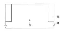
도 1을 참조하면, 반도체기판(51)의 소정영역에 활성영역(52)을 한정하는 소자분리막(53)이 제공될 수 있다.Referring to FIG. 1, an
상기 반도체기판(51)은 제 1 형 불순물 이온들을 갖는 실리콘웨이퍼일 수 있다. 상기 소자분리막(53)은 상기 활성영역(52)의 측벽들을 둘러싸도록 배치될 수 있다. 상기 소자분리막(53)은 실리콘산화막, 실리콘질화막, 실리콘산질화막, 또는 이들의 조합막과 같은 절연막일 수 있다. 상기 제 1 형은 P 형 또는 N 형일 수 있다.The
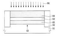
상기 활성영역(52)은 레트로그레이드 영역(retrograde region; 62), 상부 채널영역(63), 및 소스/드레인 영역들(92)을 구비할 수 있다.The
상기 레트로그레이드 영역(62)의 상부표면은 상기 소자분리막(53)의 바닥보다 상부레벨에 배치할 수 있다. 이 경우에, 상기 레트로그레이드 영역(62)은 상기 소자분리막(53)의 측벽들에 접촉될 수 있다. 상기 레트로그레이드 영역(62)은 제 2 형 불순물 이온들을 구비할 수 있다. 상기 제 2 형 불순물 이온들은 상기 제 1 형 불순물 이온들과 다른 도전형을 갖는다. 상기 제 1 형이 상기 P 형인 경우 상기 제 2 형은 상기 N형일 수 있으며, 상기 제 1 형이 상기 N 형인 경우 상기 제 2 형은 상기 P형일 수 있다.The upper surface of the
이하에서는, 상기 제 1 형은 상기 P 형이고, 상기 제 2 형은 상기 N형인 경우를 상정하여 설명하기로 한다. 이 경우에, 상기 제 2 형 불순물 이온들은 N 형 불순물 이온들일 수 있으며, 상기 N 형 불순물 이온들은 인(phosphorus) 또는 비소(arsenic)일 수 있다. 그리고 본 발명의 실시 예에서 상기 레트로그레이드 영역(62)은 상기 인(phosphorus)을 함유할 수 있다. 또한, 상기 제 1 형 불순물 이온들은 P 형 불순물 이온들일 수 있으며, 상기 P 형 불순물 이온들은 붕소(B) 또는 불화붕소(BF2)일 수 있다.Hereinafter, a case in which the first type is the P type and the second type is the N type will be described. In this case, the second type impurity ions may be N type impurity ions, and the N type impurity ions may be phosphorus or arsenic. In addition, in the embodiment of the present invention, the
상기 상부 채널영역(63)은 상기 레트로그레이드 영역(62) 상에 배치될 수 있다. 상기 상부 채널영역(63)은 상기 레트로그레이드 영역(62)의 상부표면에 접촉될 수 있다. 상기 상부 채널영역(63)은 상기 제 1 형 불순물 이온들을 구비할 수 있다. 즉, 상기 상부 채널영역(63)은 붕소(B) 또는 불화붕소(BF2)를 함유할 수 있다.The
상기 소스/드레인 영역들(92)은 상기 상부 채널영역(63) 상에 서로 이격되도록 배치될 수 있다. 상기 소스/드레인 영역들(92)은 상기 상부 채널영역(63)의 상부표면에 접촉될 수 있다. 상기 소스/드레인 영역들(92)은 상기 제 2 형 불순물 이온들을 구비할 수 있다. 상기 소스/드레인 영역들(92)은 차례로 적층된 저농도 불순물영역(64) 및 고농도 불순물영역(91)을 포함할 수 있다.The source /
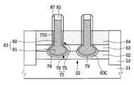
상기 활성영역(52)에 형성된 게이트 트렌치(77)를 채우는 게이트전극(83)이 제공될 수 있다. 상기 게이트전극(83)은 폴리실리콘막, 금속막, 금속 실리사이드막, 또는 이들의 조합막과 같은 도전막일 수 있다.A
상기 게이트 트렌치(77)는 상부 트렌치(75) 및 하부 트렌치(76)를 구비할 수 있다. 상기 상부 트렌치(75)는 상기 소스/드레인 영역들(92) 사이를 가로지르도록 배치될 수 있다. 상기 하부 트렌치(76)는 상기 상부 트렌치(75)의 하부에 연결될 수 있다. 상기 하부 트렌치(76)는 상기 상부 트렌치(75)보다 큰 폭을 구비할 수 있다. 상기 하부 트렌치(76)는 상기 레트로그레이드 영역(62)의 상부표면보다 낮은 레벨에 바닥을 갖는 것일 수 있다. 즉, 상기 하부 트렌치(76)는 상기 상부 채널영역(63)을 관통하여 상기 레트로그레이드 영역(62) 내에 연장될 수 있다. 상기 하부 트렌치(76)는 구형일 수 있다.The
상기 게이트전극(83)은 상기 상부 트렌치(75)를 채우는 상부 게이트전극(82) 및 상기 하부 트렌치(76)를 채우는 하부 게이트전극(81)을 포함할 수 있다. 상기 하부 게이트전극(81)은 구형일 수 있다.The
상기 하부 게이트전극(81) 및 상기 레트로그레이드 영역(62) 사이에 상기 제 1 형 불순물 이온들을 갖는 하부 채널영역(63C)이 개재될 수 있다. 즉, 상기 하부 채널영역(63C)은 붕소(B) 또는 불화붕소(BF2)를 함유할 수 있다. 상기 하부 채널영역(63C)은 상기 활성영역(52) 내에 배치될 수 있다.A
상기 게이트전극(83)은 상기 상부 채널영역(63)을 가로지르도록 배치될 수 있다. 이 경우에, 상기 상부 채널영역(63)은 상기 게이트전극(83)의 양측에 분리될 수 있다. 상기 하부 채널영역(63C)의 일단은 상기 분리된 상부 채널영역들(63) 중 하나에 접촉될 수 있다. 상기 하부 채널영역(63C)의 타단은 상기 분리된 상부 채널영역들(63)중 다른 하나에 접촉될 수 있다. 결과적으로, 상기 분리된 상부 채널영역들(63)은 상기 하부 채널영역(63C)에 의하여 전기적으로 접속될 수 있다.The
상기 상부 게이트전극(82) 및 상기 소스/드레인 영역들(92) 사이에 절연성 스페이서(75S)가 개재될 수 있다. 상기 절연성 스페이서(75S)는 실리콘질화막, 실리콘산화막, 실리콘산질화막, 또는 이들의 조합막일 수 있다. 그러나 상기 절연성 스페이서(75S)는 생략될 수 있다.An insulating
상기 게이트전극(83) 및 상기 활성영역(52) 사이에 게이트유전막(79)이 개재 될 수 있다. 상기 게이트유전막(79)은 실리콘질화막, 실리콘산화막, 실리콘산질화막, 고유전막(high-k dielectrics), 또는 이들의 조합막과 같은 절연막일 수 있다. 구체적으로, 상기 게이트유전막(79)은 상기 절연성 스페이서(75S) 및 상기 상부 게이트전극(82) 사이에 개재될 수 있으며, 상기 게이트유전막(79)은 상기 상부 채널영역(63) 및 상기 하부 게이트전극(81) 사이에 개재될 수 있고, 상기 게이트유전막(79)은 상기 하부 채널영역(63C) 및 상기 하부 게이트전극(81) 사이에 개재될 수 있다. 상기 게이트전극(83)은 상기 게이트유전막(79)에 의하여 상기 활성영역(52)으로부터 절연될 수 있다.A
상기 상부 게이트전극(82) 상에 절연패턴(85)이 제공될 수 있다. 상기 절연패턴(85)은 실리콘질화막, 실리콘산화막, 실리콘산질화막, 또는 이들의 조합막과 같은 절연막일 수 있다.An insulating
상기 상부 게이트전극(82)은 상기 소스/드레인 영역들(92) 보다 상부레벨에 돌출될 수 있다. 이 경우에, 상기 절연패턴(85) 및 상기 상부 게이트전극(82)의 측벽들 상에 게이트 스페이서들(87)이 배치될 수 있다. 상기 게이트 스페이서들(87)은 실리콘질화막, 실리콘산화막, 실리콘산질화막, 또는 이들의 조합막과 같은 절연막일 수 있다.The
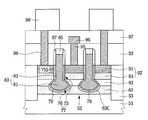
이와는 달리, 다른 실시 예에 있어서, 상기 절연패턴(85) 및 상기 상부 게이트전극(82)은 상기 소스/드레인 영역들(92)의 상부표면들 보다 낮은 레벨에 배치될 수도 있다. 이 경우에, 상기 절연패턴(85) 및 상기 상부 게이트전극(82)은 상기 상부 트렌치(75) 내에 배치될 수 있다.Alternatively, in another embodiment, the insulating
상기 게이트전극(83)을 갖는 상기 반도체기판(51)의 전면은 하부 절연막(93)으로 덮일 수 있다. 상기 하부 절연막(93)은 실리콘질화막, 실리콘산화막, 실리콘산질화막, 저유전막(low-k dielectrics), 또는 이들의 조합막일 수 있다. 상기 하부 절연막(93)은 평탄화된 상부표면을 구비할 수 있다.The entire surface of the
상기 하부 절연막(93) 상에 비트 라인(96)이 배치될 수 있다. 상기 비트라인(96)은 상기 하부 절연막(93)을 관통하는 비트 플러그(bit plug; 95)에 의하여 상기 소스/드레인 영역들(92) 중 선택된 하나에 전기적으로 접속될 수 있다. 즉, 상기 비트 플러그(95)의 일단은 상기 비트라인(96)에 접촉될 수 있으며, 상기 비트 플러그(95)의 타단은 상기 소스/드레인 영역들(92) 중 선택된 하나에 접촉될 수 있다. 상기 비트 플러그(95) 및 상기 비트라인(96)은 폴리실리콘막, 금속막, 금속 실리사이드막, 또는 이들의 조합막과 같은 도전막일 수 있다.The
상기 비트라인(96) 및 상기 하부 절연막(93)은 상부 절연막(97)으로 덮일 수 있다. 상기 상부 절연막(97)은 실리콘질화막, 실리콘산화막, 실리콘산질화막, 저유전막(low-k dielectrics), 또는 이들의 조합막일 수 있다. 상기 상부 절연막(97)은 평탄화된 상부표면을 구비할 수 있다.The
상기 상부 절연막(97) 상에 스토리지 노드(storage node; 99)가 배치될 수 있다. 상기 스토리지 노드(99)는 커패시터의 하부전극일 수 있다. 상기 스토리지 노드(99)는 폴리실리콘막, 금속막, 금속 실리사이드막, 또는 이들의 조합막과 같은 도전막일 수 있다.A
상기 스토리지 노드(99)는 상기 상부 절연막(97) 및 상기 하부 절연막(93)을 차례로 관통하는 매립 콘택플러그 (buried contact plug; 98)에 의하여 상기 소스/드레인 영역들(92) 중 선택된 다른 하나에 전기적으로 접속될 수 있다. 즉, 상기 매립 콘택플러그(98)의 일단은 상기 스토리지 노드(99)에 접촉될 수 있으며, 상기 매립 콘택플러그(98)의 타단은 상기 소스/드레인 영역들(92) 중 선택된 다른 하나에 접촉될 수 있다. 상기 매립 콘택플러그(98)는 폴리실리콘막, 금속막, 금속 실리사이드막, 또는 이들의 조합막과 같은 도전막일 수 있다.The
상기 게이트전극(83)에 문턱전압 이상의 게이트전압이 인가되면 상기 게이트전극(83)의 하단표면에 대응하는 상기 상부 채널영역(63) 및 상기 하부 채널영역(63C)에 채널(channel)이 형성될 수 있다. 즉, 상기 게이트 트렌치(77)를 이용하여 유효 채널 길이를 증가시킬 수 있다.When a gate voltage of more than a threshold voltage is applied to the
상기 반도체기판(51)에는 바디 바이어스(body bias; VB)가 인가될 수 있다. 이 경우에, 상기 상부 채널영역(63) 및 상기 하부 채널영역(63C)은 상기 레트로그레이드 영역(62)에 의하여 상기 반도체기판(51)으로부터 전기적으로 고립될 수 있다. 이에 따라, 상기 바디 바이어스(VB)에 의존하여 문턱전압이 상승하는 것을 효율적으로 제어 할 수 있다.A body bias VB may be applied to the
도 2 내지 도 9는 본 발명의 제 1 실시 예에 따른 레트로그레이드 영역을 갖는 반도체소자의 제조방법을 설명하기 위한 단면도들이다.2 to 9 are cross-sectional views illustrating a method of manufacturing a semiconductor device having a retrograde area according to a first embodiment of the present invention.
도 2를 참조하면, 반도체기판(51)의 소정영역에 활성영역(52)을 한정하는 소자분리막(53)을 형성할 수 있다.Referring to FIG. 2, an
상기 반도체기판(51)은 제 1 형 불순물 이온들을 갖는 실리콘웨이퍼로 형성할 수 있다. 상기 소자분리막(53)은 트렌치소자분리 기술을 이용하여 형성할 수 있다. 상기 소자분리막(53)은 상기 활성영역(52)의 측벽들을 둘러싸도록 형성될 수 있다. 상기 소자분리막(53)은 실리콘산화막, 실리콘질화막, 실리콘산질화막, 또는 이들의 조합막과 같은 절연막으로 형성할 수 있다. 상기 제 1 형은 P 형 또는 N 형일 수 있다.The
이하에서는, 상기 제 1 형은 상기 P 형인 경우를 상정하여 설명하기로 한다. 이 경우에, 상기 제 1 형 불순물 이온들은 P 형 불순물 이온들일 수 있으며, 상기 P 형 불순물 이온들은 붕소(B) 또는 불화붕소(BF2)일 수 있다.Hereinafter, the first type will be described assuming the case of the P type. In this case, the first type impurity ions may be P type impurity ions, and the P type impurity ions may be boron (B) or boron fluoride (BF2 ).
도 3을 참조하면, 상기 활성영역(52)에 제 1 이온주입 공정(60)을 이용하여 제 2 형 불순물 이온들을 주입하여 레트로그레이드 영역(retrograde region; 62)을 형성할 수 있다. 상기 레트로그레이드 영역(62)은 상기 소자분리막(53)의 측벽들에 접촉되도록 형성할 수 있다. 상기 레트로그레이드 영역(62)의 상부표면은 상기 소자분리막(53)의 바닥보다 상부레벨에 형성할 수 있다.Referring to FIG. 3, a
상기 제 2 형 불순물 이온들은 상기 제 1 형 불순물 이온들과 다른 도전형을 갖는다. 상기 제 1 형이 상기 P 형인 경우 상기 제 2 형은 상기 N형일 수 있으며, 상기 제 1 형이 상기 N 형인 경우 상기 제 2 형은 상기 P형일 수 있다.The second type impurity ions have a different conductivity type from the first type impurity ions. When the first type is the P type, the second type may be the N type, and when the first type is the N type, the second type may be the P type.
이하에서는, 상기 제 1 형은 상기 P 형이고, 상기 제 2 형은 상기 N형인 경우를 상정하여 설명하기로 한다. 이 경우에, 상기 제 2 형 불순물 이온들은 N 형 불순물 이온들일 수 있으며, 상기 N 형 불순물 이온들은 인(phosphorus) 또는 비소(arsenic)일 수 있다. 그리고 본 발명의 제 1 실시 예에서 상기 레트로그레이드 영역(62)은 상기 인(phosphorus)을 함유할 수 있다.Hereinafter, a case in which the first type is the P type and the second type is the N type will be described. In this case, the second type impurity ions may be N type impurity ions, and the N type impurity ions may be phosphorus or arsenic. In addition, in the first embodiment of the present invention, the
상기 레트로그레이드 영역(62) 상의 상기 활성영역(52)에 상기 제 1 형 불순물 이온들을 주입하여 상부 채널영역(63)을 형성할 수 있다. 이 경우에, 상기 상부 채널영역(63)은 붕소(B) 또는 불화붕소(BF2)를 함유할 수 있다. 상기 상부 채널영역(63)은 상기 레트로그레이드 영역(62)의 상부표면에 접촉되도록 형성할 수 있다.The
상기 상부 채널영역(63) 상의 상기 활성영역(52)에 상기 제 2 형 불순물 이온들을 주입하여 저농도 불순물영역(64)을 형성할 수 있다. 상기 저농도 불순물영역(64)은 상기 상부 채널영역(63)의 상부표면에 접촉되도록 형성할 수 있다.The low
그 결과, 상기 레트로그레이드 영역(62), 상기 상부 채널영역(63) 및 상기 저농도 불순물영역(64)은 상기 활성영역(52) 내에 차례로 적층될 수 있다. 또한, 상기 상부 채널영역(63)은 상기 레트로그레이드 영역(62)에 의하여 상기 반도체기판(51)으로부터 전기적으로 고립될 수 있다.As a result, the
그러나 본 발명의 다른 실시 예에서, 상기 저농도 불순물영역(64)을 형성하는 것은 생략될 수 있다. 이 경우에, 상기 저농도 불순물영역(64)은 후속공정을 이용하여 형성할 수 있다. 또 다른 실시 예에서, 상기 상부 채널영역(63) 및 상기 저농도 불순물영역(64)은 모두 생략될 수 있다. 이 경우에, 상기 상부 채널영역(63) 및 상기 저농도 불순물영역(64)은 후속공정을 이용하여 형성할 수 있다.However, in another embodiment of the present invention, forming the low
도 4를 참조하면, 상기 반도체기판(51) 상에 상기 활성영역(52)을 부분적으로 노출시키는 개구부(73A)를 갖는 하드마스크 패턴(73)을 형성할 수 있다. 상기 하드마스크 패턴(73)은 차례로 적층된 버퍼막(71) 및 마스크막(72)으로 형성할 수 있다.Referring to FIG. 4, a
상기 버퍼막(71)은 화학기상증착(chemical vapor deposition; CVD) 방법 또는 열산화(thermal oxidation) 방법에 의한 실리콘산화막으로 형성할 수 있다. 상기 마스크막(72)은 실리콘질화막과 같은 질화막으로 형성할 수 있다.The
상기 하드마스크 패턴(73)을 식각마스크로 사용하여 상기 노출된 활성영역(52)을 식각하여 상부 트렌치(75)를 형성할 수 있다. 상기 상부 트렌치(75)는 상기 활성영역(52)을 가로지르도록 형성할 수 있다. 상기 노출된 활성영역(52)을 식각하는 것은 이방성 식각 공정을 이용하여 상기 상부 채널영역(63)이 노출될 때 까지 수행할 수 있다. 이 경우에, 상기 저농도 불순물영역(64)은 상기 상부 트렌치(75)의 양측에 분할될 수 있다. 즉, 상기 상부 트렌치(75)의 양측에 서로 이격된 한 쌍의 상기 저농도 불순물영역들(64)이 잔존할 수 있다.The
도 5를 참조하면, 상기 상부 트렌치(75) 내의 측벽들에 절연성 스페이서(75S)를 형성할 수 있다. 상기 절연성 스페이서(75S)는 상기 활성영역(52)에 대하여 식각선택비를 갖는 물질막으로 형성할 수 있다. 상기 절연성 스페이서(75S)는 실리콘질화막, 실리콘산화막, 실리콘산질화막, 또는 이들의 조합막으로 형성할 수 있다.Referring to FIG. 5, an insulating
상기 절연성 스페이서(75S) 및 상기 하드마스크 패턴(73)을 식각마스크로 사 용하여 상기 노출된 상부 채널영역(63) 및 상기 레트로그레이드 영역(62)을 식각하여 하부 트렌치(76)를 형성할 수 있다. 상기 노출된 상부 채널영역(63) 및 상기 레트로그레이드 영역(62)을 식각하는 것은 등방성 식각 공정, 이방성 식각 공정, 또는 이들의 조합을 이용하여 수행할 수 있다.The
상기 하부 트렌치(76)는 상기 상부 트렌치(75)의 하부에 연결될 수 있다. 상기 하부 트렌치(76)는 상기 상부 트렌치(75)보다 큰 폭으로 형성할 수 있다. 상기 하부 트렌치(76)의 바닥은 상기 레트로그레이드 영역(62)의 상부표면보다 낮은 레벨에 형성할 수 있다. 즉, 상기 하부 트렌치(76)는 상기 상부 채널영역(63)을 관통하여 상기 레트로그레이드 영역(62) 내에 연장될 수 있다. 상기 하부 트렌치(76)는 구형으로 형성할 수 있다.The
상기 상부 트렌치(75) 및 상기 하부 트렌치(76)는 게이트 트렌치(77)를 구성할 수 있다. 그 결과, 상기 저농도 불순물영역(64) 및 상기 상부 채널영역(63)의 각각은 상기 게이트 트렌치(77)의 양측에 분할될 수 있다. 상기 게이트 트렌치(77)의 바닥은 상기 레트로그레이드 영역(62) 내에 연장될 수 있다. 즉, 상기 게이트 트렌치(77) 내에 상기 레트로그레이드 영역(62), 상기 상부 채널영역들(63) 및 상기 절연성 스페이서(75S)가 노출될 수 있다.The
도 6을 참조하면, 상기 노출된 레트로그레이드 영역(62)에 제 2 이온주입 공정(60C)을 이용하여 상기 제 1 형 불순물 이온들을 주입하여 하부 채널영역(63C)을 형성할 수 있다. 이 경우에, 상기 하부 채널영역(63C)은 붕소(B) 또는 불화붕 소(BF2)를 함유할 수 있다. 상기 하부 채널영역(63C)은 상기 게이트 트렌치(77)의 바닥표면을 따라 형성될 수 있다. 상기 하부 채널영역(63C)의 하부에 상기 레트로그레이드 영역(62)이 잔존할 수 있다.Referring to FIG. 6, the
상기 하부 채널영역(63C)의 일단은 상기 분리된 상부 채널영역들(63) 중 하나에 접촉될 수 있다. 상기 하부 채널영역(63C)의 타단은 상기 분리된 상부 채널영역들(63)중 다른 하나에 접촉될 수 있다. 결과적으로, 상기 분리된 상부 채널영역들(63)은 상기 하부 채널영역(63C)에 의하여 전기적으로 접속될 수 있다.One end of the
도 7을 참조하면, 상기 게이트 트렌치(77)에 게이트유전막(79)을 형성할 수 있다. 상기 게이트유전막(79)은 실리콘질화막, 실리콘산화막, 실리콘산질화막, 고유전막(high-k dielectrics), 또는 이들의 조합막과 같은 절연막으로 형성할 수 있다. 상기 게이트유전막(79)은 상기 게이트 트렌치(77)의 내벽을 따라 균일한 두께로 형성될 수 있다. 이 경우에, 상기 게이트유전막(79)은 상기 절연성 스페이서(75S), 상기 노출된 상부 채널영역들(63) 및 상기 하부 채널영역(63C)을 덮도록 형성될 수 있다.Referring to FIG. 7, a
상기 게이트 트렌치(77)에 게이트전극(83)을 형성할 수 있다. 상기 게이트전극(83)은 폴리실리콘막, 금속막, 금속 실리사이드막, 또는 이들의 조합막과 같은 도전막으로 형성할 수 있다. 상기 게이트전극(83)은 상기 상부 트렌치(75)를 채우는 상부 게이트전극(82) 및 상기 하부 트렌치(76)를 채우는 하부 게이트전극(81)을 포함할 수 있다. 상기 하부 게이트전극(81)은 상기 상부 게이트전극(82)보다 큰 폭 으로 형성할 수 있다. 상기 하부 게이트전극(81)은 구형으로 형성할 수 있다.A
상기 상부 게이트전극(82) 상에 절연패턴(85)을 형성할 수 있다. 상기 절연패턴(85)은 실리콘질화막, 실리콘산화막, 실리콘산질화막, 또는 이들의 조합막과 같은 절연막으로 형성할 수 있다.An insulating
이어서, 상기 하드마스크 패턴(73)을 제거하여 상기 저농도 불순물영역(64)을 노출시킬 수 있다. 상기 상부 게이트전극(82)은 상기 저농도 불순물영역(64) 보다 상부레벨에 돌출될 수 있다. 이 경우에, 상기 절연패턴(85) 및 상기 상부 게이트전극(82)의 측벽들 상에 게이트 스페이서들(87)을 형성할 수 있다. 상기 게이트 스페이서들(87)은 실리콘질화막, 실리콘산화막, 실리콘산질화막, 또는 이들의 조합막과 같은 절연막으로 형성할 수 있다.Subsequently, the
다른 방법으로, 상기 하드마스크 패턴(73)을 제거하는 동안 상기 절연패턴(85)이 함께 식각되어 제거되거나 일부만 잔존될 수 있다.Alternatively, the insulating
또 다른 방법으로, 상기 하드마스크 패턴(73)은 상기 게이트전극(83)을 형성하기 전에 제거할 수 있다. 이 경우에, 상기 상부 게이트전극(82) 및 상기 절연패턴(85)은 상기 상부 트렌치(75) 내에 형성할 수 있다. 즉, 상기 상부 게이트전극(82)은 상기 저농도 불순물영역들(64)의 상부표면 보다 낮은 레벨에 형성할 수 있다.As another method, the
이하에서는, 상기 상부 게이트전극(82)은 상기 저농도 불순물영역들(64) 보다 상부레벨에 돌출된 경우를 상정하여 설명하기로 한다.Hereinafter, the case where the
도 8을 참조하면, 상기 게이트전극(83), 상기 절연패턴(85) 및 상기 게이트 스페이서들(87)을 이온주입 마스크로 사용하여 상기 노출된 저농도 불순물영역들(64)에 제 3 이온주입 공정(89)을 이용하여 상기 제 2 형 불순물 이온들을 주입하여 고농도 불순물영역들(91)을 형성할 수 있다. 그 결과, 상기 저농도 불순물영역들(64)은 상기 고농도 불순물영역들(91)의 하부에 잔존할 수 있다.Referring to FIG. 8, a third ion implantation process is performed on the exposed low
상기 저농도 불순물영역들(64) 및 상기 고농도 불순물영역들(91)은 소스/드레인 영역들(92)을 구성할 수 있다. 즉, 상기 소스/드레인 영역들(92)은 상기 게이트전극(83) 양측에 서로 이격되어 형성될 수 있다. 상기 소스/드레인 영역들(92)은 상기 상부 채널영역들(63)에 접촉될 수 있다.The low
도 9를 참조하면, 상기 반도체기판(51)의 전면 상을 덮는 하부 절연막(93)을 형성할 수 있다. 상기 하부 절연막(93)은 실리콘질화막, 실리콘산화막, 실리콘산질화막, 저유전막(low-k dielectrics), 또는 이들의 조합막으로 형성할 수 있다. 상기 하부 절연막(93)은 상기 게이트전극(83)을 덮을 수 있다. 상기 하부 절연막(93)을 평탄화하여 평평한 상부표면을 형성할 수 있다.Referring to FIG. 9, a lower insulating
상기 하부 절연막(93)을 관통하는 비트 플러그(bit plug; 95)를 형성할 수 있다. 상기 하부 절연막(93) 상에 상기 비트 플러그(95)와 접촉되는 비트 라인(96)을 형성할 수 있다. 상기 비트 플러그(95)는 상기 소스/드레인 영역들(92)중 선택된 하나에 접촉될 수 있다. 즉, 상기 비트 라인(96)은 상기 비트 플러그(95)를 경유하여 상기 소스/드레인 영역들(92)중 선택된 하나에 전기적으로 접속될 수 있다. 상기 비트 플러그(95) 및 상기 비트 라인(96)은 폴리실리콘막, 금속막, 금속실리사이드막, 또는 이들의 조합막과 같은 도전막으로 형성할 수 있다.A bit plug 95 may be formed to penetrate the lower insulating
상기 하부 절연막(93)을 덮는 상부 절연막(97)을 형성할 수 있다. 상기 상부 절연막(97)은 실리콘질화막, 실리콘산화막, 실리콘산질화막, 저유전막(low-k dielectrics), 또는 이들의 조합막으로 형성할 수 있다. 상기 상부 절연막(97)은 상기 비트 라인(96)을 덮을 수 있다. 상기 상부 절연막(97)을 평탄화하여 평평한 상부표면을 형성할 수 있다.An upper insulating
상기 상부 절연막(97) 및 상기 하부 절연막(93)을 차례로 관통하여 상기 소스/드레인 영역들(92) 중 선택된 다른 하나에 접촉된 매립 콘택플러그 (buried contact plug; 98)를 형성할 수 있다. 상기 매립 콘택플러그(98)는 폴리실리콘막, 금속막, 금속 실리사이드막, 또는 이들의 조합막과 같은 도전막으로 형성할 수 있다.A buried
상기 상부 절연막(97) 상에 상기 매립 콘택플러그(98)와 접촉되는 스토리지 노드(storage node; 99)를 형성할 수 있다. 상기 스토리지 노드(99)는 커패시터의 하부전극일 수 있다. 상기 스토리지 노드(99)는 폴리실리콘막, 금속막, 금속 실리사이드막, 또는 이들의 조합막과 같은 도전막으로 형성할 수 있다. 상기 스토리지 노드(99)는 상기 매립 콘택플러그(98)를 경유하여 상기 소스/드레인 영역들(92) 중 선택된 다른 하나에 전기적으로 접속될 수 있다.A
도 10은 본 발명의 제 2 실시 예에 따른 레트로그레이드 영역을 갖는 반도체소자의 제조방법을 설명하기 위한 단면도이다.10 is a cross-sectional view illustrating a method of manufacturing a semiconductor device having a retrograde area according to a second embodiment of the present invention.
도 10을 참조하면, 본 발명의 제 2 실시 예에 따른 반도체소자의 제조방법은 도 2를 참조하여 설명된 상기 활성영역(52) 및 상기 소자분리막(53)을 형성하는 것 을 포함할 수 있다. 이하에서는, 차이점만 간략하게 설명하기로 한다.Referring to FIG. 10, a method of manufacturing a semiconductor device according to the second embodiment of the present invention may include forming the
상기 활성영역(52)에 제 4 이온주입 공정(60A)을 이용하여 상기 제 2 형 불순물 이온들을 주입하여 레트로그레이드 영역(retrograde region; 62)을 형성할 수 있다. 상기 레트로그레이드 영역(62)은 상기 소자분리막(53)의 측벽들에 접촉되도록 형성할 수 있다. 상기 레트로그레이드 영역(62)의 상부표면은 상기 소자분리막(53)의 바닥보다 상부레벨에 형성할 수 있다.The
상기 제 2 형 불순물 이온들은 N 형 불순물 이온들일 수 있으며, 상기 N 형 불순물 이온들은 인(phosphorus) 또는 비소(arsenic)일 수 있다. 그리고 본 발명의 제 2 실시 예에서 상기 레트로그레이드 영역(62)은 상기 인(phosphorus)을 함유할 수 있다.The second type impurity ions may be N type impurity ions, and the N type impurity ions may be phosphorus or arsenic. In addition, in the second embodiment of the present invention, the
상기 레트로그레이드 영역(62) 상의 상기 활성영역(52)에 상기 제 1 형 불순물 이온들을 주입하여 상부 채널영역(63)을 형성할 수 있다. 이 경우에, 상기 상부 채널영역(63)은 붕소(B) 또는 불화붕소(BF2)를 함유할 수 있다. 상기 상부 채널영역(63)은 상기 레트로그레이드 영역(62)의 상부표면에 접촉되도록 형성할 수 있다.The
그 결과, 상기 레트로그레이드 영역(62) 및 상기 상부 채널영역(63)은 상기 활성영역(52) 내에 차례로 적층될 수 있다. 또한, 상기 상부 채널영역(63)은 상기 레트로그레이드 영역(62)에 의하여 상기 반도체기판(51)으로부터 전기적으로 고립될 수 있다.As a result, the
그러나 본 발명의 다른 실시 예에서, 상기 상부 채널영역(63)을 형성하는 것 은 생략될 수 있다. 이 경우에, 상기 상부 채널영역(63)은 후속공정을 이용하여 형성할 수 있다.However, in another embodiment of the present invention, forming the
도 11은 본 발명의 제 3 실시 예에 따른 레트로그레이드 영역을 갖는 반도체소자의 제조방법을 설명하기 위한 단면도이다.11 is a cross-sectional view for describing a method of manufacturing the semiconductor device having the retrograde region according to the third embodiment of the present invention.
도 11을 참조하면, 본 발명의 제 3 실시 예에 따른 반도체소자의 제조방법은 도 2를 참조하여 설명된 상기 활성영역(52) 및 상기 소자분리막(53)을 형성하는 것을 포함할 수 있다. 이하에서는, 차이점만 간략하게 설명하기로 한다.Referring to FIG. 11, the method of manufacturing a semiconductor device according to the third exemplary embodiment may include forming the
상기 활성영역(52)에 제 5 이온주입 공정(60B)을 이용하여 상기 제 2 형 불순물 이온들을 주입하여 레트로그레이드 영역(retrograde region; 62)을 형성할 수 있다. 상기 레트로그레이드 영역(62)은 상기 소자분리막(53)의 측벽들에 접촉되도록 형성할 수 있다. 상기 레트로그레이드 영역(62)의 상부표면은 상기 소자분리막(53)의 바닥보다 상부레벨에 형성할 수 있다.A
상기 제 2 형 불순물 이온들은 N 형 불순물 이온들일 수 있으며, 상기 N 형 불순물 이온들은 인(phosphorus) 또는 비소(arsenic)일 수 있다. 그리고 본 발명의 제 3 실시 예에서 상기 레트로그레이드 영역(62)은 상기 인(phosphorus)을 함유할 수 있다.The second type impurity ions may be N type impurity ions, and the N type impurity ions may be phosphorus or arsenic. In addition, in the third embodiment of the present invention, the
상기 레트로그레이드 영역(62) 상의 상기 활성영역(52)에 상기 제 1 형 불순물 이온들을 주입하여 상부 채널영역(63)을 형성할 수 있다. 이 경우에, 상기 상부 채널영역(63)은 붕소(B) 또는 불화붕소(BF2)를 함유할 수 있다. 상기 상부 채널영 역(63)은 상기 레트로그레이드 영역(62)의 상부표면에 접촉되도록 형성할 수 있다.The
상기 상부 채널영역(63) 상의 상기 활성영역(52)에 상기 제 2 형 불순물 이온들을 주입하여 저농도 불순물영역(64)을 형성할 수 있다. 상기 저농도 불순물영역(64)은 상기 상부 채널영역(63)의 상부표면에 접촉되도록 형성할 수 있다.The low
상기 저농도 불순물영역(64)에 상기 제 2 형 불순물 이온들을 주입하여 고농도 불순물영역(91)을 형성할 수 있다. 상기 고농도 불순물영역(91)은 상기 저농도 불순물영역(64)의 표면을 따라 형성할 수 있다. 그 결과, 상기 저농도 불순물영역(64)은 상기 고농도 불순물영역(91)의 하부에 잔존할 수 있다.The high
결과적으로, 상기 레트로그레이드 영역(62), 상기 상부 채널영역(63), 상기 저농도 불순물영역(64) 및 상기 고농도 불순물영역(91)은 상기 활성영역(52) 내에 차례로 적층될 수 있다. 또한, 상기 상부 채널영역(63)은 상기 레트로그레이드 영역(62)에 의하여 상기 반도체기판(51)으로부터 전기적으로 고립될 수 있다.As a result, the
<실험 예>Experimental Example
[표1]은 본 발명의 실시 예에 따른 바디 효과(body-effect)에 의한 문턱전압의 변화를 알아보기 위한 실험결과이다.[Table 1] is an experimental result to determine the change in the threshold voltage due to the body effect (body-effect) according to an embodiment of the present invention.
[표1]에 있어서, 상기 시료 1 및 상기 시료 2는 게이트 길이(gate length) 35nm, 게이트 폭(gate width) 50nm, 및 게이트 트렌치의 깊이(gate trench depth) 180nm를 갖도록 제작하였다. 상기 시료 2는 레트로그레이드 영역 형성을 위한 인(phosphorus) 이온주입 공정을 수행하였으며, 상기 시료 1은 상기 레트로그레이드 영역 형성을 위한 이온주입 공정을 생략하였다. 상기 시료 2의 상기 레트로그레이드 영역 형성을 위한 인(phosphorus) 이온주입 공정은 180KV 의 에너지 및 5E+12 atoms/㎠ 의 도즈(dose)로 수행하였다.In Table 1, Sample 1 and Sample 2 were manufactured to have a gate length of 35 nm, a gate width of 50 nm, and a gate trench depth of 180 nm. The sample 2 performed a phosphorus ion implantation process for forming a retrograde region, and the sample 1 omitted an ion implantation process for forming a retrograde region. Phosphorus ion implantation process for forming the retrograde region of Sample 2 was performed with energy of 180 KV and dose of 5E + 12 atoms / cm 2.
[표1]을 참조하면, 상기 시료 1 의 문턱전압은 0.699 V 로 측정되었으며, 상기 시료 2의 문턱전압은 0.683 V 로 측정되었다. 즉, 상기 시료 1 및 상기 시료 2 의 문턱전압들은 비슷한 레벨을 보임을 알 수 있다. 그리고 상기 시료 1 의 바디 바이어스(body bias)에 의한 문턱전압 변화율(BE)은 0.287 V/-1V 로 측정되었으며, 상기 시료 2 의 바디 바이어스(body bias)에 의한 문턱전압 변화율(BE)은 0.162 V/-1V 로 측정되었다. 즉, 상기 시료 2 의 바디 바이어스(body bias)에 의한 문턱전압 변화율(BE)은 상기 시료 1에 비하여 약50% 감소함을 알 수 있다.Referring to Table 1, the threshold voltage of the sample 1 was measured as 0.699 V, and the threshold voltage of the sample 2 was measured as 0.683 V. That is, it can be seen that the threshold voltages of the sample 1 and the sample 2 have similar levels. The threshold voltage change rate (BE) due to the body bias of the sample 1 was measured at 0.287 V / -1V, and the threshold voltage change rate BE due to the body bias of the sample 2 was 0.162 V. It was measured at / -1V. That is, it can be seen that the threshold voltage change rate (BE) due to the body bias of the sample 2 is reduced by about 50% compared to the sample 1.
결론적으로, 본 발명의 실시 예에 따르면 상기 레트로그레이드 영역을 이용하여 바디 효과(body-effect)에 의한 문턱전압 상승을 효율적으로 제어할 수 있다.In conclusion, according to an exemplary embodiment of the present invention, the threshold voltage increase due to a body effect may be efficiently controlled by using the retrograde region.
상술한 바와 같이 본 발명에 따르면, 제 1 형 불순물 이온들을 갖는 반도체기판에 활성영역이 한정된다. 상기 활성영역은 레트로그레이드 영역(retrograde region), 상부 채널영역, 하부 채널영역 및 서로 이격된 한 쌍의 소스/드레인 영역들을 구비할 수 있다. 상기 레트로그레이드 영역은 제 2 형 불순물 이온들을 갖는다. 상기 활성영역에 형성된 게이트 트렌치를 채우는 게이트전극이 제공된다. 상기 게이트전극은 상기 소스/드레인 영역들 사이에 배치되고 상기 상부 채널영역을 관통하여 상기 레트로그레이드 영역 내에 신장된다. 이에 따라, 상기 게이트전극에 문턱전압 이상의 게이트전압이 인가되면 상기 게이트전극의 하단표면에 대응하는 상기 상부 채널영역 및 상기 하부 채널영역에 채널(channel)이 형성될 수 있다. 즉, 상기 게이트 트렌치를 이용하여 유효 채널 길이를 증가시킬 수 있다.As described above, according to the present invention, the active region is defined in the semiconductor substrate having the first type impurity ions. The active region may include a retrograde region, an upper channel region, a lower channel region, and a pair of source / drain regions spaced apart from each other. The retrograde region has second type impurity ions. A gate electrode is provided to fill a gate trench formed in the active region. The gate electrode is disposed between the source / drain regions and extends into the retrograde region through the upper channel region. Accordingly, when a gate voltage of more than a threshold voltage is applied to the gate electrode, a channel may be formed in the upper channel region and the lower channel region corresponding to the bottom surface of the gate electrode. That is, the effective channel length can be increased by using the gate trench.
또한, 상기 상부 채널영역 및 상기 하부 채널영역은 상기 레트로그레이드 영역에 의하여 상기 반도체기판으로부터 전기적으로 고립될 수 있다. 이에 따라, 바디 바이어스(body bias)에 의존하여 상기 문턱전압이 상승하는 것을 효율적으로 제어 할 수 있다.In addition, the upper channel region and the lower channel region may be electrically isolated from the semiconductor substrate by the retrograde region. Accordingly, it is possible to efficiently control the increase of the threshold voltage depending on the body bias.
결과적으로, 유효 채널 길이를 증가시키면서 바디 효과(body effect)에 의한 문턱전압의 상승을 방지할 수 있는 반도체소자를 구현할 수 있다.As a result, a semiconductor device capable of preventing an increase in a threshold voltage due to a body effect while increasing the effective channel length can be implemented.
Claims (25)
Translated fromKoreanPriority Applications (3)
| Application Number | Priority Date | Filing Date | Title |
|---|---|---|---|
| KR1020070004308AKR100819562B1 (en) | 2007-01-15 | 2007-01-15 | Semiconductor device having retrograde area and manufacturing method thereof |
| US11/809,252US20080169493A1 (en) | 2007-01-15 | 2007-05-31 | Semiconductor devices and dynamic random access memories having a retrograde region and methods of forming the same |
| CNA2008100029822ACN101226959A (en) | 2007-01-15 | 2008-01-15 | Dynamic random access memory, semiconductor device and method of forming same |
Applications Claiming Priority (1)
| Application Number | Priority Date | Filing Date | Title |
|---|---|---|---|
| KR1020070004308AKR100819562B1 (en) | 2007-01-15 | 2007-01-15 | Semiconductor device having retrograde area and manufacturing method thereof |
Publications (1)
| Publication Number | Publication Date |
|---|---|
| KR100819562B1true KR100819562B1 (en) | 2008-04-08 |
Family
ID=39533819
Family Applications (1)
| Application Number | Title | Priority Date | Filing Date |
|---|---|---|---|
| KR1020070004308AExpired - Fee RelatedKR100819562B1 (en) | 2007-01-15 | 2007-01-15 | Semiconductor device having retrograde area and manufacturing method thereof |
Country Status (3)
| Country | Link |
|---|---|
| US (1) | US20080169493A1 (en) |
| KR (1) | KR100819562B1 (en) |
| CN (1) | CN101226959A (en) |
Families Citing this family (67)
| Publication number | Priority date | Publication date | Assignee | Title |
|---|---|---|---|---|
| KR100854501B1 (en)* | 2007-02-23 | 2008-08-26 | 삼성전자주식회사 | Morse transistor having recess channel region and method of manufacturing same |
| KR100825815B1 (en)* | 2007-06-07 | 2008-04-28 | 삼성전자주식회사 | A semiconductor device having an active pattern having a channel recess portion and a method of manufacturing the same |
| US8097916B2 (en)* | 2007-07-23 | 2012-01-17 | Infineon Technologies Austria Ag | Method for insulating a semiconducting material in a trench from a substrate |
| JP2009224520A (en)* | 2008-03-14 | 2009-10-01 | Elpida Memory Inc | Semiconductor device and method of manufacturing semiconductor device |
| JP2010003916A (en)* | 2008-06-20 | 2010-01-07 | Elpida Memory Inc | Semiconductor device and method of manufacturing the same |
| US8421162B2 (en) | 2009-09-30 | 2013-04-16 | Suvolta, Inc. | Advanced transistors with punch through suppression |
| US8273617B2 (en) | 2009-09-30 | 2012-09-25 | Suvolta, Inc. | Electronic devices and systems, and methods for making and using the same |
| US8530286B2 (en) | 2010-04-12 | 2013-09-10 | Suvolta, Inc. | Low power semiconductor transistor structure and method of fabrication thereof |
| KR20110124584A (en)* | 2010-05-11 | 2011-11-17 | 삼성전자주식회사 | Semiconductor device having recess channel transistor and manufacturing method thereof |
| US8569128B2 (en) | 2010-06-21 | 2013-10-29 | Suvolta, Inc. | Semiconductor structure and method of fabrication thereof with mixed metal types |
| US8759872B2 (en) | 2010-06-22 | 2014-06-24 | Suvolta, Inc. | Transistor with threshold voltage set notch and method of fabrication thereof |
| US8377783B2 (en) | 2010-09-30 | 2013-02-19 | Suvolta, Inc. | Method for reducing punch-through in a transistor device |
| US8404551B2 (en) | 2010-12-03 | 2013-03-26 | Suvolta, Inc. | Source/drain extension control for advanced transistors |
| US8461875B1 (en) | 2011-02-18 | 2013-06-11 | Suvolta, Inc. | Digital circuits having improved transistors, and methods therefor |
| US8525271B2 (en) | 2011-03-03 | 2013-09-03 | Suvolta, Inc. | Semiconductor structure with improved channel stack and method for fabrication thereof |
| US8400219B2 (en) | 2011-03-24 | 2013-03-19 | Suvolta, Inc. | Analog circuits having improved transistors, and methods therefor |
| US8748270B1 (en) | 2011-03-30 | 2014-06-10 | Suvolta, Inc. | Process for manufacturing an improved analog transistor |
| US8999861B1 (en) | 2011-05-11 | 2015-04-07 | Suvolta, Inc. | Semiconductor structure with substitutional boron and method for fabrication thereof |
| US8796048B1 (en) | 2011-05-11 | 2014-08-05 | Suvolta, Inc. | Monitoring and measurement of thin film layers |
| US8811068B1 (en) | 2011-05-13 | 2014-08-19 | Suvolta, Inc. | Integrated circuit devices and methods |
| US8569156B1 (en) | 2011-05-16 | 2013-10-29 | Suvolta, Inc. | Reducing or eliminating pre-amorphization in transistor manufacture |
| US8735987B1 (en) | 2011-06-06 | 2014-05-27 | Suvolta, Inc. | CMOS gate stack structures and processes |
| US8995204B2 (en) | 2011-06-23 | 2015-03-31 | Suvolta, Inc. | Circuit devices and methods having adjustable transistor body bias |
| US8629016B1 (en) | 2011-07-26 | 2014-01-14 | Suvolta, Inc. | Multiple transistor types formed in a common epitaxial layer by differential out-diffusion from a doped underlayer |
| US8609492B2 (en)* | 2011-07-27 | 2013-12-17 | Micron Technology, Inc. | Vertical memory cell |
| KR101891373B1 (en) | 2011-08-05 | 2018-08-24 | 엠아이이 후지쯔 세미컨덕터 리미티드 | Semiconductor devices having fin structures and fabrication methods thereof |
| US8748986B1 (en) | 2011-08-05 | 2014-06-10 | Suvolta, Inc. | Electronic device with controlled threshold voltage |
| US8645878B1 (en) | 2011-08-23 | 2014-02-04 | Suvolta, Inc. | Porting a circuit design from a first semiconductor process to a second semiconductor process |
| US8614128B1 (en) | 2011-08-23 | 2013-12-24 | Suvolta, Inc. | CMOS structures and processes based on selective thinning |
| US8713511B1 (en) | 2011-09-16 | 2014-04-29 | Suvolta, Inc. | Tools and methods for yield-aware semiconductor manufacturing process target generation |
| JP5609939B2 (en)* | 2011-09-27 | 2014-10-22 | 株式会社デンソー | Semiconductor device |
| US9236466B1 (en) | 2011-10-07 | 2016-01-12 | Mie Fujitsu Semiconductor Limited | Analog circuits having improved insulated gate transistors, and methods therefor |
| US8895327B1 (en) | 2011-12-09 | 2014-11-25 | Suvolta, Inc. | Tipless transistors, short-tip transistors, and methods and circuits therefor |
| US8819603B1 (en) | 2011-12-15 | 2014-08-26 | Suvolta, Inc. | Memory circuits and methods of making and designing the same |
| US8883600B1 (en) | 2011-12-22 | 2014-11-11 | Suvolta, Inc. | Transistor having reduced junction leakage and methods of forming thereof |
| US8599623B1 (en) | 2011-12-23 | 2013-12-03 | Suvolta, Inc. | Circuits and methods for measuring circuit elements in an integrated circuit device |
| US8877619B1 (en) | 2012-01-23 | 2014-11-04 | Suvolta, Inc. | Process for manufacture of integrated circuits with different channel doping transistor architectures and devices therefrom |
| US8970289B1 (en) | 2012-01-23 | 2015-03-03 | Suvolta, Inc. | Circuits and devices for generating bi-directional body bias voltages, and methods therefor |
| US9093550B1 (en) | 2012-01-31 | 2015-07-28 | Mie Fujitsu Semiconductor Limited | Integrated circuits having a plurality of high-K metal gate FETs with various combinations of channel foundation structure and gate stack structure and methods of making same |
| US9406567B1 (en) | 2012-02-28 | 2016-08-02 | Mie Fujitsu Semiconductor Limited | Method for fabricating multiple transistor devices on a substrate with varying threshold voltages |
| US8863064B1 (en) | 2012-03-23 | 2014-10-14 | Suvolta, Inc. | SRAM cell layout structure and devices therefrom |
| JP5852913B2 (en)* | 2012-03-27 | 2016-02-03 | ルネサスエレクトロニクス株式会社 | Semiconductor device |
| US9299698B2 (en) | 2012-06-27 | 2016-03-29 | Mie Fujitsu Semiconductor Limited | Semiconductor structure with multiple transistors having various threshold voltages |
| US8637955B1 (en) | 2012-08-31 | 2014-01-28 | Suvolta, Inc. | Semiconductor structure with reduced junction leakage and method of fabrication thereof |
| US9112057B1 (en) | 2012-09-18 | 2015-08-18 | Mie Fujitsu Semiconductor Limited | Semiconductor devices with dopant migration suppression and method of fabrication thereof |
| US9041126B2 (en) | 2012-09-21 | 2015-05-26 | Mie Fujitsu Semiconductor Limited | Deeply depleted MOS transistors having a screening layer and methods thereof |
| US9431068B2 (en) | 2012-10-31 | 2016-08-30 | Mie Fujitsu Semiconductor Limited | Dynamic random access memory (DRAM) with low variation transistor peripheral circuits |
| US8816754B1 (en) | 2012-11-02 | 2014-08-26 | Suvolta, Inc. | Body bias circuits and methods |
| US9093997B1 (en) | 2012-11-15 | 2015-07-28 | Mie Fujitsu Semiconductor Limited | Slew based process and bias monitors and related methods |
| US9070477B1 (en) | 2012-12-12 | 2015-06-30 | Mie Fujitsu Semiconductor Limited | Bit interleaved low voltage static random access memory (SRAM) and related methods |
| US9112484B1 (en) | 2012-12-20 | 2015-08-18 | Mie Fujitsu Semiconductor Limited | Integrated circuit process and bias monitors and related methods |
| US9268885B1 (en) | 2013-02-28 | 2016-02-23 | Mie Fujitsu Semiconductor Limited | Integrated circuit device methods and models with predicted device metric variations |
| US8994415B1 (en) | 2013-03-01 | 2015-03-31 | Suvolta, Inc. | Multiple VDD clock buffer |
| US8988153B1 (en) | 2013-03-09 | 2015-03-24 | Suvolta, Inc. | Ring oscillator with NMOS or PMOS variation insensitivity |
| US9299801B1 (en) | 2013-03-14 | 2016-03-29 | Mie Fujitsu Semiconductor Limited | Method for fabricating a transistor device with a tuned dopant profile |
| US9449967B1 (en) | 2013-03-15 | 2016-09-20 | Fujitsu Semiconductor Limited | Transistor array structure |
| CN104051524B (en)* | 2013-03-15 | 2017-12-05 | 英飞凌科技奥地利有限公司 | Semiconductor devices |
| US9112495B1 (en) | 2013-03-15 | 2015-08-18 | Mie Fujitsu Semiconductor Limited | Integrated circuit device body bias circuits and methods |
| US9478571B1 (en) | 2013-05-24 | 2016-10-25 | Mie Fujitsu Semiconductor Limited | Buried channel deeply depleted channel transistor |
| US8976575B1 (en) | 2013-08-29 | 2015-03-10 | Suvolta, Inc. | SRAM performance monitor |
| US9710006B2 (en) | 2014-07-25 | 2017-07-18 | Mie Fujitsu Semiconductor Limited | Power up body bias circuits and methods |
| US9319013B2 (en) | 2014-08-19 | 2016-04-19 | Mie Fujitsu Semiconductor Limited | Operational amplifier input offset correction with transistor threshold voltage adjustment |
| KR102354463B1 (en)* | 2015-01-09 | 2022-01-24 | 삼성전자주식회사 | Semiconducor devices having retrograde channels and methods for fabricating the same |
| KR102303300B1 (en)* | 2017-08-04 | 2021-09-16 | 삼성전자주식회사 | Semiconductor device |
| CN112038340B (en)* | 2019-06-04 | 2024-08-23 | 长鑫存储技术有限公司 | Memory structure and forming method thereof |
| CN113078113B (en)* | 2020-01-03 | 2023-01-31 | 长鑫存储技术有限公司 | Semiconductor structure and preparation method thereof |
| CN115775821A (en)* | 2021-09-06 | 2023-03-10 | 长鑫存储技术有限公司 | Semiconductor structure and manufacturing method thereof |
Citations (2)
| Publication number | Priority date | Publication date | Assignee | Title |
|---|---|---|---|---|
| KR20040069795A (en)* | 2003-01-30 | 2004-08-06 | 아남반도체 주식회사 | Method for manufacturing semiconductor device with fluorine implant |
| JP2006049897A (en) | 2004-07-30 | 2006-02-16 | Internatl Business Mach Corp <Ibm> | Method of manufacturing ultra-thin body field effect transistor (FET) device and ultra-thin body FET device manufactured thereby (ultra-thin body ultra-steep retrograde well (SSRW) FET device) |
Family Cites Families (7)
| Publication number | Priority date | Publication date | Assignee | Title |
|---|---|---|---|---|
| US6342709B1 (en)* | 1997-12-10 | 2002-01-29 | The Kansai Electric Power Co., Inc. | Insulated gate semiconductor device |
| US6018174A (en)* | 1998-04-06 | 2000-01-25 | Siemens Aktiengesellschaft | Bottle-shaped trench capacitor with epi buried layer |
| EP1271654B1 (en)* | 2001-02-01 | 2017-09-20 | Mitsubishi Denki Kabushiki Kaisha | Semiconductor device and method of manufacturing the same |
| DE10214066B4 (en)* | 2002-03-28 | 2007-02-01 | Advanced Micro Devices, Inc., Sunnyvale | Semiconductor device having a retrograde doping profile in a channel region and method of making the same |
| US8338887B2 (en)* | 2005-07-06 | 2012-12-25 | Infineon Technologies Ag | Buried gate transistor |
| JP4773169B2 (en)* | 2005-09-14 | 2011-09-14 | エルピーダメモリ株式会社 | Manufacturing method of semiconductor device |
| US7476932B2 (en)* | 2006-09-29 | 2009-01-13 | The Boeing Company | U-shape metal-oxide-semiconductor (UMOS) gate structure for high power MOS-based semiconductor devices |
- 2007
- 2007-01-15KRKR1020070004308Apatent/KR100819562B1/ennot_activeExpired - Fee Related
- 2007-05-31USUS11/809,252patent/US20080169493A1/ennot_activeAbandoned
- 2008
- 2008-01-15CNCNA2008100029822Apatent/CN101226959A/enactivePending
Patent Citations (2)
| Publication number | Priority date | Publication date | Assignee | Title |
|---|---|---|---|---|
| KR20040069795A (en)* | 2003-01-30 | 2004-08-06 | 아남반도체 주식회사 | Method for manufacturing semiconductor device with fluorine implant |
| JP2006049897A (en) | 2004-07-30 | 2006-02-16 | Internatl Business Mach Corp <Ibm> | Method of manufacturing ultra-thin body field effect transistor (FET) device and ultra-thin body FET device manufactured thereby (ultra-thin body ultra-steep retrograde well (SSRW) FET device) |
Also Published As
| Publication number | Publication date |
|---|---|
| US20080169493A1 (en) | 2008-07-17 |
| CN101226959A (en) | 2008-07-23 |
Similar Documents
| Publication | Publication Date | Title |
|---|---|---|
| KR100819562B1 (en) | Semiconductor device having retrograde area and manufacturing method thereof | |
| US7615449B2 (en) | Semiconductor device having a recess channel transistor | |
| US8530962B2 (en) | Transistor of semiconductor device and method for manufacturing the same | |
| US6780732B2 (en) | DRAM access transistor | |
| US7701002B2 (en) | Semiconductor device having buried gate electrode and method of fabricating the same | |
| US9245975B2 (en) | Recessed channel insulated-gate field effect transistor with self-aligned gate and increased channel length | |
| US8053307B2 (en) | Method of fabricating semiconductor device with cell epitaxial layers partially overlap buried cell gate electrode | |
| US7268043B2 (en) | Semiconductor device and method of manufacturing the same | |
| US7910989B2 (en) | Semiconductor device with increased channel area and decreased leakage current | |
| US20070252198A1 (en) | Semiconductor device having a fin channel transistor | |
| US20080242024A1 (en) | Method of manufacturing semiconductor device | |
| CN101546772A (en) | Semiconductor device including capacitor element and manufacturing method thereof | |
| US10825931B2 (en) | Semiconductor device with undercutted-gate and method of fabricating the same | |
| US20080073730A1 (en) | Semiconductor device and method for formimg the same | |
| US20120175709A1 (en) | Semiconductor device and method of manufacturing the same | |
| US8658491B2 (en) | Manufacturing method of transistor structure having a recessed channel | |
| KR100668511B1 (en) | Fin transistor and its manufacturing method | |
| US20110298040A1 (en) | Semiconductor device and method of manufacturing the same | |
| US7265039B2 (en) | Method for fabricating semiconductor device with improved refresh time | |
| US7354827B2 (en) | Transistor having asymmetric channel region, semiconductor device including the same, and method of fabricating semiconductor device including the same | |
| KR20070070890A (en) | Fin transistor and its manufacturing method | |
| US7279741B2 (en) | Semiconductor device with increased effective channel length and method of manufacturing the same | |
| KR100951573B1 (en) | Semiconductor device and manufacturing method thereof | |
| KR20250087884A (en) | Semiconductor device | |
| US7652323B2 (en) | Semiconductor device having step gates and method of manufacturing the same |
Legal Events
| Date | Code | Title | Description |
|---|---|---|---|
| A201 | Request for examination | ||
| PA0109 | Patent application | St.27 status event code:A-0-1-A10-A12-nap-PA0109 | |
| PA0201 | Request for examination | St.27 status event code:A-1-2-D10-D11-exm-PA0201 | |
| D13-X000 | Search requested | St.27 status event code:A-1-2-D10-D13-srh-X000 | |
| D14-X000 | Search report completed | St.27 status event code:A-1-2-D10-D14-srh-X000 | |
| E701 | Decision to grant or registration of patent right | ||
| PE0701 | Decision of registration | St.27 status event code:A-1-2-D10-D22-exm-PE0701 | |
| GRNT | Written decision to grant | ||
| PR0701 | Registration of establishment | St.27 status event code:A-2-4-F10-F11-exm-PR0701 | |
| PR1002 | Payment of registration fee | St.27 status event code:A-2-2-U10-U11-oth-PR1002 Fee payment year number:1 | |
| PG1601 | Publication of registration | St.27 status event code:A-4-4-Q10-Q13-nap-PG1601 | |
| LAPS | Lapse due to unpaid annual fee | ||
| PC1903 | Unpaid annual fee | St.27 status event code:A-4-4-U10-U13-oth-PC1903 Not in force date:20110329 Payment event data comment text:Termination Category : DEFAULT_OF_REGISTRATION_FEE | |
| PC1903 | Unpaid annual fee | St.27 status event code:N-4-6-H10-H13-oth-PC1903 Ip right cessation event data comment text:Termination Category : DEFAULT_OF_REGISTRATION_FEE Not in force date:20110329 | |
| R18-X000 | Changes to party contact information recorded | St.27 status event code:A-5-5-R10-R18-oth-X000 | |
| P22-X000 | Classification modified | St.27 status event code:A-4-4-P10-P22-nap-X000 | |
| P22-X000 | Classification modified | St.27 status event code:A-4-4-P10-P22-nap-X000 |