KR100819104B1 - Parallel bit test circuit and parallel bit test method - Google Patents
Parallel bit test circuit and parallel bit test methodDownload PDFInfo
- Publication number
- KR100819104B1 KR100819104B1KR1020060086008AKR20060086008AKR100819104B1KR 100819104 B1KR100819104 B1KR 100819104B1KR 1020060086008 AKR1020060086008 AKR 1020060086008AKR 20060086008 AKR20060086008 AKR 20060086008AKR 100819104 B1KR100819104 B1KR 100819104B1
- Authority
- KR
- South Korea
- Prior art keywords
- data
- clock signal
- output
- parallel bit
- compressed
- Prior art date
- Legal status (The legal status is an assumption and is not a legal conclusion. Google has not performed a legal analysis and makes no representation as to the accuracy of the status listed.)
- Expired - Fee Related
Links
Images


Classifications
- G—PHYSICS
- G11—INFORMATION STORAGE
- G11C—STATIC STORES
- G11C29/00—Checking stores for correct operation ; Subsequent repair; Testing stores during standby or offline operation
- G11C29/04—Detection or location of defective memory elements, e.g. cell constructio details, timing of test signals
- G11C29/08—Functional testing, e.g. testing during refresh, power-on self testing [POST] or distributed testing
- G11C29/12—Built-in arrangements for testing, e.g. built-in self testing [BIST] or interconnection details
- G11C29/18—Address generation devices; Devices for accessing memories, e.g. details of addressing circuits
- G11C29/30—Accessing single arrays
- G11C29/34—Accessing multiple bits simultaneously
- G—PHYSICS
- G11—INFORMATION STORAGE
- G11C—STATIC STORES
- G11C11/00—Digital stores characterised by the use of particular electric or magnetic storage elements; Storage elements therefor
- G11C11/21—Digital stores characterised by the use of particular electric or magnetic storage elements; Storage elements therefor using electric elements
- G11C11/34—Digital stores characterised by the use of particular electric or magnetic storage elements; Storage elements therefor using electric elements using semiconductor devices
- G11C11/40—Digital stores characterised by the use of particular electric or magnetic storage elements; Storage elements therefor using electric elements using semiconductor devices using transistors
- G11C11/401—Digital stores characterised by the use of particular electric or magnetic storage elements; Storage elements therefor using electric elements using semiconductor devices using transistors forming cells needing refreshing or charge regeneration, i.e. dynamic cells
- G—PHYSICS
- G11—INFORMATION STORAGE
- G11C—STATIC STORES
- G11C29/00—Checking stores for correct operation ; Subsequent repair; Testing stores during standby or offline operation
- G11C29/04—Detection or location of defective memory elements, e.g. cell constructio details, timing of test signals
- G11C29/08—Functional testing, e.g. testing during refresh, power-on self testing [POST] or distributed testing
- G11C29/12—Built-in arrangements for testing, e.g. built-in self testing [BIST] or interconnection details
- G11C29/12015—Built-in arrangements for testing, e.g. built-in self testing [BIST] or interconnection details comprising clock generation or timing circuitry
- G—PHYSICS
- G11—INFORMATION STORAGE
- G11C—STATIC STORES
- G11C29/00—Checking stores for correct operation ; Subsequent repair; Testing stores during standby or offline operation
- G11C29/04—Detection or location of defective memory elements, e.g. cell constructio details, timing of test signals
- G11C29/08—Functional testing, e.g. testing during refresh, power-on self testing [POST] or distributed testing
- G11C29/12—Built-in arrangements for testing, e.g. built-in self testing [BIST] or interconnection details
- G11C29/38—Response verification devices
- G11C29/40—Response verification devices using compression techniques
- G—PHYSICS
- G11—INFORMATION STORAGE
- G11C—STATIC STORES
- G11C11/00—Digital stores characterised by the use of particular electric or magnetic storage elements; Storage elements therefor
- G11C11/21—Digital stores characterised by the use of particular electric or magnetic storage elements; Storage elements therefor using electric elements
- G11C11/34—Digital stores characterised by the use of particular electric or magnetic storage elements; Storage elements therefor using electric elements using semiconductor devices
- G11C11/40—Digital stores characterised by the use of particular electric or magnetic storage elements; Storage elements therefor using electric elements using semiconductor devices using transistors
- G11C11/41—Digital stores characterised by the use of particular electric or magnetic storage elements; Storage elements therefor using electric elements using semiconductor devices using transistors forming static cells with positive feedback, i.e. cells not needing refreshing or charge regeneration, e.g. bistable multivibrator or Schmitt trigger
- G—PHYSICS
- G11—INFORMATION STORAGE
- G11C—STATIC STORES
- G11C29/00—Checking stores for correct operation ; Subsequent repair; Testing stores during standby or offline operation
- G11C29/04—Detection or location of defective memory elements, e.g. cell constructio details, timing of test signals
- G11C29/08—Functional testing, e.g. testing during refresh, power-on self testing [POST] or distributed testing
- G11C29/12—Built-in arrangements for testing, e.g. built-in self testing [BIST] or interconnection details
- G11C2029/1204—Bit line control
- G—PHYSICS
- G11—INFORMATION STORAGE
- G11C—STATIC STORES
- G11C29/00—Checking stores for correct operation ; Subsequent repair; Testing stores during standby or offline operation
- G11C29/04—Detection or location of defective memory elements, e.g. cell constructio details, timing of test signals
- G11C29/08—Functional testing, e.g. testing during refresh, power-on self testing [POST] or distributed testing
- G11C29/12—Built-in arrangements for testing, e.g. built-in self testing [BIST] or interconnection details
- G11C29/18—Address generation devices; Devices for accessing memories, e.g. details of addressing circuits
- G11C29/26—Accessing multiple arrays
- G11C2029/2602—Concurrent test
Landscapes
- Engineering & Computer Science (AREA)
- Microelectronics & Electronic Packaging (AREA)
- Computer Hardware Design (AREA)
- For Increasing The Reliability Of Semiconductor Memories (AREA)
- Dram (AREA)
Abstract
Translated fromKorean
Description
Translated fromKorean도 1은 종래의 반도체 메모리 장치의 병렬 비트 테스트 회로의 일례를 간략히 보인 블록도.1 is a block diagram schematically showing an example of a parallel bit test circuit of a conventional semiconductor memory device.
도 2는 데이터 압축부의 일례를 보인 논리 회로도.2 is a logic circuit diagram showing an example of a data compression unit.
도 3은 에러교정을 위한 패리티 셀 영역의 추가로 인해 메모리 어레이의 크기가 50% 더 증가된 경우의 병렬 비트 테스트를 설명하기 위한 블록도.3 is a block diagram illustrating a parallel bit test in the case where the size of the memory array is increased by 50% further due to the addition of a parity cell region for error correction.
도 4는 버스트 길이가 2인 경우를 설명하기 위한 타이밍도.4 is a timing diagram for explaining the case where the burst length is two;
도 5는 본 발명의 일 실시예에 따른 반도체 메모리 장치의 병렬 비트 테스트 회로의 블록도.5 is a block diagram of a parallel bit test circuit of a semiconductor memory device according to an embodiment of the present invention.
도 6은 도 5에서 n 이 24이고 버스트 길이가 3인 경우를 예시한 블록도.FIG. 6 is a block diagram illustrating a case where n is 24 and a burst length is 3 in FIG. 5; FIG.
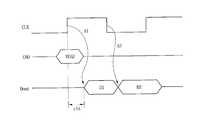
도 7은 도 6에서 버스트 길이가 3인 경우를 설명하기 위한 타이밍도.FIG. 7 is a timing diagram for explaining the case where the burst length is 3 in FIG. 6; FIG.
도 8은 도 6에서의 딜레이부의 일례를 보인 회로도.FIG. 8 is a circuit diagram illustrating an example of a delay unit in FIG. 6. FIG.
<도면의 주요부분에 대한 부호의 설명><Description of the symbols for the main parts of the drawings>
DL : 데이터 라인DL: data line
50 ~ 55, 61 ~ 68, 71 ~ 74 : 데이터 압축부50 to 55, 61 to 68, 71 to 74: data compression section
56 : 메모리 어레이57, 77 : 버스 폭 변환부56:
58, 78 : 딜레이부CLK : 클럭신호58, 78: delay unit CLK: clock signal
CLKD : 딜레이된 클럭BLCS : 버스트 길이 제어신호CLKD: Delayed Clock BLCS: Burst Length Control Signal
INV1 ~ INV4 : 인버터MC1 ~ MC4 : 모스 커패시터INV1 to INV4: Inverter MC1 to MC4: Morse Capacitor
본 발명은 반도체 메모리 장치의 병렬 비트 테스트 회로 및 병렬 비트 테스트 방법에 관한 것으로서, 보다 상세하게는 내부적으로 데이터 라인의 수가 늘어나는 경우, 특히 에러 교정(error correction)을 위한 패리티 비트(parity bit) 인해 비트 수가 증가하더라도 테스트 타임의 증가없이 출력 핀의 수를 줄임으로써 테스트 장비의 채널 부족 문제를 극복할 수 있는 병렬 비트 테스트 회로 및 병렬 비트 테스트 방법에 관한 것이다.BACKGROUND OF THE
일반적으로, 디램(DRAM ; Dynamic Random Access memory)과 같은 반도체 메모리 장치의 경우에는 데이터(data)의 리드(read) 및 라이트(write) 동작이 정확하게 이루어져야 한다. 이와 같이 데이터의 리드 및 라이트 동작이 정확하게 이루어지기 위해서는 칩 내에 불량 셀(cell)이 존재하여서는 아니된다.In general, in the case of a semiconductor memory device such as a dynamic random access memory (DRAM), read and write operations of data must be accurately performed. As described above, in order to accurately read and write data, a defective cell should not exist in the chip.
그러나, 반도체 메모리 장치의 초고집적화 추세에 따라 하나의 칩에 집적되 는 셀의 수가 수천만 개 또는 그 이상으로 되어감에 따라 칩의 제조 공정의 발달에도 불구하고 불량 셀의 존재 가능성은 더욱 커진다. 그리고, 상기 칩에 대한 정확한 테스트가 수행되어져 불량 셀을 포함하는 칩을 선별해 내지 않는다면, 그러한 불량 셀을 포함하는 칩은 신뢰성이 확보될 수 없다.However, as the number of cells integrated in a single chip increases to tens of millions or more in accordance with the trend of ultra-high integration of semiconductor memory devices, the possibility of the presence of defective cells increases even with the development of the chip manufacturing process. And, unless the accurate test is performed on the chip to select chips containing defective cells, the chips containing such defective cells cannot be secured.
반도체 메모리 장치의 테스트에 있어서 중요한 이슈는 테스트의 신뢰성 및 테스트 타임으로 크게 두 가지로 나눠 볼 수 있다. 이 중 특히 후자인 테스트 타임에 관해 살펴보면, 수천만 개의 셀에 대해 고속으로 테스트하여 테스트 타임을 감소시키는 것은, 반도체 메모리 장치의 제품 개발 기간의 단축과 아울러 제품 출하시까지의 테스트 타임 단축이 제품의 비용(cost)과 직결된다는 면에서 생산의 효율성 및 제조업체 간의 경쟁에 있어서 매우 중요한 이슈이다.There are two major issues in testing semiconductor memory devices: reliability of test and test time. In particular, in the latter test time, reducing the test time by testing at tens of millions of cells at high speed is not only shortening the product development period of the semiconductor memory device but also reducing the test time until the product is shipped. It is a very important issue in production efficiency and competition among manufacturers in terms of cost.
일반적으로, 반도체 메모리 장치에서는, 반도체 메모리 장치 내의 메모리 셀의 양/불량(pass/fail) 여부를 가리고자 할 때, 만약 한 개의 셀 씩 테스트한다면, 고집적화 또는 초고집적화된 반도체 메모리 장치의 테스트 타임은 길어지고 비용도 증가하게 된다.In general, in a semiconductor memory device, in order to mask the pass / fail of memory cells in a semiconductor memory device, if one cell is tested one by one, the test time of a highly integrated or ultra-integrated semiconductor memory device is It will be longer and more expensive.
따라서, 테스트 타임을 줄이기 위해 병렬 비트 테스트(parallel bit test)가 사용된다.Therefore, parallel bit test is used to reduce test time.
웨이퍼 상태에 있는 칩의 양/불량을 구분하기 위해, EDS(Electro Die Sorting) 단계에서 칩에서의 불량 처리된 셀 어드레스(cell address)를 판별하여 해당 셀을 리페어하는 경우에도 마찬가지로 상기 병렬 비트 테스트는 유용하다.In order to distinguish between the quantity of chips in a wafer state and a defect, the parallel bit test may be performed in the case of repairing a corresponding cell by determining a defective cell address in a chip in an electro die sorting (EDS) step. useful.
예를 들어, 상기 병렬 비트 테스트는 다수의 셀에 같은 데이터를 라이트한 후, 리드시 배타 논리합(exclusive OR) 회로를 이용하여, 같은 데이터가 읽혀지면 양(pass)으로 처리하고, 하나라도 다른 데이터가 읽혀지면 불량(fail)으로 처리한다. 그리하여, 상기 병렬 비트 테스트는 테스트 타임을 단축할 수 있다.For example, the parallel bit test writes the same data to a plurality of cells, and then uses an exclusive OR circuit at read time to process the same data when it is read, and pass one data to another. If is read, it is treated as a failure. Thus, the parallel bit test can shorten the test time.
이하에서는 첨부된 도면을 참조하여, 종래의 병렬 비트 테스트에 관하여 설명한다.Hereinafter, a conventional parallel bit test will be described with reference to the accompanying drawings.
도 1은 종래의 반도체 메모리 장치의 병렬 비트 테스트 회로의 일례를 간략히 보인 블록도이다.1 is a block diagram schematically illustrating an example of a parallel bit test circuit of a conventional semiconductor memory device.
도 1을 참조하면, 메모리 어레이(16) 및 복수의 데이터 압축부들(10 ~ 15)이 도시되어 있다.Referring to FIG. 1, a
상기 메모리 어레이(16)는 매트릭스 형태로 배열된 복수의 메모리 셀들(미도시)을 구비한다. 그리고, 상기 복수의 메모리 셀들 각각에는 대응되는 데이터라인이 연결되어져 있다.The
상기 데이터 압축부(10 ~ 15) 각각은 배타 논리합 회로를 포함한다.Each of the
상기 배타 논리합 회로(eXclusive OR ; XOR)를 포함하는 데이터 압축부(10)에 대한 일례는 도 2에 도시되어 있다.An example of the
도 2를 참조하면, 데이터 라인들(DL0, DL1, DL2, DL3)에 연결된 두 개의 배타 논리합 회로(21, 22)로 리드하고자 하는 데이터가 인가되면, 상기 배타 논리합 회로(21)는 데이터 라인들(DL0, DL2)에서 출력되는 데이터에 대해 배타 논리합(XOR) 연산을 수행하고, 상기 배타 논리합 회로(22)는 데이터 라인들(DL1, DL3)에서 출력되는 데이터에 대해 배타 논리합(XOR) 연산을 수행한다. 그리고, 논리합 회로(23)는 상기 배타 논리합 회로(21, 22)의 배타 논리합 연산 결과를 수신하여 논리합(OR) 연산을 수행한 후 출력 핀(DQ0)으로 출력한다. 상기 데이터 압축부(10)이외의 다른 데이터 압축부들(11 ~ 15)의 경우에도 도 2에 도시된 회로와 동일하다.Referring to FIG. 2, when data to be read is applied to two exclusive OR
다시 도 1을 참조하면, 하나의 워드라인(미도시)을 활성화시키면, 총 4 x 16개의 데이터 비트들을 한꺼번에 읽어낸다. 상기 데이터 압축부(10 ~ 15) 각각에 연결된 복수의 데이터 라인들은 네 개다. 하나의 데이터 압축부에 연결된 데이터 라인들이 네 개보다 더 많거나 더 적을 수 있지만, 도 2에서는 네 개인 경우가 예시되어 있다.Referring back to FIG. 1, when one word line (not shown) is activated, a total of 4 x 16 data bits are read at a time. Four data lines connected to each of the
따라서, 상기 데이터 압축부(10 ~ 15) 각각은 4 비트(4 bits)의 데이터를 1 비트로 압축하는 개념으로 볼 수 있다.Therefore, each of the
예를 들어, 데이터 라인들(DL[3:0])로 인가되는 데이터가 하나라도 다르면, 데이터 압축부(10)는 논리 '1'을 출력 핀(DQ0)으로 출력한다. 반대로, 상기 데이터 라인들(DL[3:0])로 인가되는 데이터가 모두 같으면, 데이터 압축부(10)는 논리 '0'을 출력 핀(DQ0)으로 출력한다.For example, if any data applied to the data lines DL [3: 0] is different, the
버스트 길이(burst length)가 1인 경우에는 병렬 비트 테스트에 사용되는 출력 핀들은 상기 설명에서와 같이 DQ0 ~ DQ15이다. 그러나, 버스트 길이가 2인 경우에는 도시되지는 않았지만, 병렬 비트 테스트에 사용되는 출력 핀들은 그 개수가 반으로 줄어든다. 예를 들면, 버스트 길이가 2인 경우에 병렬 비트 테스트에 사용되는 출력 핀들은 DQ0, DQ2, DQ4, DQ6, DQ8, DQ10, DQ12, DQ14일 수 있다.When the burst length is 1, the output pins used for the parallel bit test are DQ0 to DQ15 as described above. However, although not shown when the burst length is 2, the number of output pins used for parallel bit testing is cut in half. For example, when the burst length is 2, the output pins used for the parallel bit test may be DQ0, DQ2, DQ4, DQ6, DQ8, DQ10, DQ12, and DQ14.
여기서, 버스트 길이(burst length)는 하나의 클럭 사이클 내에서 연속된 데이터의 개수를 나타낸다. 예를 들면, 버스트 길이가 1인 경우는 클럭신호의 상승 에지에서만 데이터를 샘플링하는 경우이고, 버스트 길이가 2인 경우는 클럭신호의 상승 에지 및 하강 에지에서 데이터를 샘플링하는 경우이다. 버스트 길이가 2인 경우는 도 4를 참조하여 설명될 수 있다.Here, the burst length represents the number of consecutive data in one clock cycle. For example, when the burst length is 1, data is sampled only at the rising edge of the clock signal, and when the burst length is 2, data is sampled at the rising edge and the falling edge of the clock signal. The case where the burst length is 2 may be described with reference to FIG. 4.
즉, 도 4는 버스트 길이가 2인 경우를 설명하기 위한 타이밍도로서 도 4를 참조하면, 클럭신호(CLK)의 상승 에지에 동기되어 리드 명령(READ)이 반도체 메모리 장치로 인가되면, 억세스 타임(tAA) 후에 출력 핀(DQ 핀)으로 데이터(D1)가 출력되고, 상기 데이터(D1)에 연속되어 데이터(D2)가 상기 출력 핀으로 출력된다. 여기서, 상기 데이터(D1)는 클럭신호(CLK)의 상승 에지에 응답하여 출력되고(A1), 상기 데이터(D2)는 클럭신호(CLK)의 하강 에지에 응답하여 출력된다(A2).That is, FIG. 4 is a timing diagram for explaining the case where the burst length is 2. Referring to FIG. 4, when the read command READ is applied to the semiconductor memory device in synchronization with the rising edge of the clock signal CLK, the access time is determined. After tAA, data D1 is output to the output pin DQ pin, and data D2 is output to the output pin in succession to the data D1. Here, the data D1 is output in response to the rising edge of the clock signal CLK (A1), and the data D2 is output in response to the falling edge of the clock signal CLK (A2).
도 3은 도 2의 메모리 어레이 영역에 에러 교정을 위한 패리티 셀 영역(parity cell area)을 추가함으로 인해 메모리 어레이의 크기가 50% 더 증가된 경우의 병렬 비트 테스트를 설명하기 위한 블록도이다.FIG. 3 is a block diagram illustrating a parallel bit test when a size of a memory array is increased by 50% by adding a parity cell area for error correction to the memory array area of FIG. 2.
도 3을 참조하면, 데이터 압축부들(31 ~ 44) 및 출력 핀들(DQ0 ~ DQ23)이 도시되어 있다.Referring to FIG. 3,
상기 데이터 압축부들(31 ~ 44)은 두 개의 그룹(30, 40)으로 그룹지어져 있다. 제1 그룹(30)은 도 1에 도시된 데이터 압축부들에 대응되는 그룹이고, 제2 그룹(40)은 패리티 비트용 데이터 압축부들이다.The
데이터에서 에러 교정을 위한 패리티 비트가 아닌 비트를 노멀 비트라고 하 면, 하나의 데이터 압축부에 연결된 데이터 라인의 개수는 네 개이므로, 상기 노멀 비트 영역의 데이터 라인들의 개수는 64개이고 상기 패리티 비트 영역의 데이터 라인들의 개수는 32개이다. 따라서, 이 경우 패리티 비트 오버헤드(parity bit overhead)는 50%이다.When the bits other than the parity bits for error correction in data are called normal bits, since the number of data lines connected to one data compression unit is four, the number of data lines in the normal bit area is 64 and the parity bit area. The number of data lines in is 32. Thus, in this case the parity bit overhead is 50%.
그에 따라, 상기 패리티 비트용 데이터 압축부의 개수는 8개이고 노멀 비트용 데이터 압축부의 개수는 16개이므로 총 데이터 압축부의 개수는 24개이다.Accordingly, since the number of data compression units for parity bits is 8 and the number of data compression units for normal bits is 16, the total number of data compression units is 24.
그리하여, 참조부호 48에서 보여지는 바와 같이, 총 96개의 데이터 비트들이 동시에 출력되므로 버스트 길이 1로 병렬 비트 테스트하기 위해서는 출력 핀의 개수가 24개여야 한다. 또한, 참조부호 49에서 보여지는 바와 같이 버스트 길이 2로 하더라도 최소한 16개의 출력 핀이 요구된다.Thus, as shown at 48, a total of 96 data bits are output simultaneously, so the number of output pins must be 24 for parallel bit testing with
그러므로, 상기와 같은 경우 테스트 장비 입장에서 볼 경우에는 하나의 테스트 장비에서 동시에 테스트할 수 있는 칩의 개수가 줄어들게 되어 테스트 타임의 증가를 가져오는 문제점이 있다.Therefore, in the above case, the number of chips that can be simultaneously tested in one test equipment is reduced in view of the test equipment, thereby increasing the test time.
따라서, 메모리 용량의 증가가 있고 입출력 라인의 증가도 있는 경우, 특히 에러 교정을 위한 패리티 비트가 추가되는 경우에 있어서 병렬 비트 테스트를 할 경우 테스트 타임의 증가를 억제하기 위한 방안이 절실히 요구된다.Therefore, when there is an increase in memory capacity and an increase in input / output lines, especially when parity bits for error correction are added, there is an urgent need for a method for suppressing an increase in test time when performing parallel bit tests.
따라서, 본 발명의 목적은 하나의 테스트 장비에서 동시에 테스트할 수 있는 칩의 개수가 줄어듦으로 인해 테스트 타임이 증가되는 문제점을 개선하기 위한 병 렬 비트 테스트 회로 및 그에 의한 병렬 비트 테스트 방법을 제공함에 있다.Accordingly, an object of the present invention is to provide a parallel bit test circuit and a parallel bit test method for improving the problem that the test time is increased by reducing the number of chips that can be tested simultaneously in one test equipment. .
본 발명의 다른 목적은 반도체 메모리 장치에 있어서 메모리 용량의 증가가 있고 입출력 라인의 증가도 있는 경우 병렬 비트 테스트의 테스트 타임의 증가를 억제할 수 있는 병렬 비트 테스트 회로 및 그에 의한 병렬 비트 테스트 방법을 제공함에 있다.Another object of the present invention is to provide a parallel bit test circuit and a parallel bit test method thereof, which can suppress an increase in test time of a parallel bit test when there is an increase in memory capacity and an increase in input / output lines in a semiconductor memory device. Is in.
본 발명의 또 다른 목적은 반도체 메모리 장치에 있어서 에러 교정을 위한 패리티 비트가 추가되는 경우에 있어서 병렬 비트 테스트를 할 경우 테스트 타임의 증가를 줄일 수 있는 병렬 비트 테스트 회로 및 그에 의한 병렬 비트 테스트 방법을 제공함에 있다.It is still another object of the present invention to provide a parallel bit test circuit and a parallel bit test method for reducing an increase in test time when a parallel bit test is performed in a case where a parity bit for error correction is added in a semiconductor memory device. In providing.
상기의 목적들을 달성하기 위한 본 발명의 일 양상에 따른 복수의 메모리 셀들이 매트릭스 형태로 배열된 메모리 어레이를 구비하는 반도체 메모리 장치의 병렬 비트 테스트 회로는, 상기 메모리 셀들에 연결된 복수의 데이터 라인들에 연결되어 상기 데이터 라인들로부터 출력되는 데이터를 수신한 후 압축함으로써 압축된 데이터를 출력하기 위한 복수의 데이터 압축부들; 클럭신호를 수신하여 딜레이된 클럭신호를 생성하기 위한 딜레이부; 및 상기 클럭신호 및 딜레이된 클럭신호에 응답하여 상기 데이터 압축부들로부터 출력되는 상기 압축된 데이터를 상기 압축된 데이터의 폭보다 작은 폭으로 변환한 후 출력단으로 출력하기 위한 버스 폭 변환부를 구비함을 특징으로 한다.A parallel bit test circuit of a semiconductor memory device having a memory array in which a plurality of memory cells are arranged in a matrix form according to an aspect of the present invention for achieving the above objects is provided in a plurality of data lines connected to the memory cells. A plurality of data compressors connected to output compressed data by receiving and outputting data output from the data lines; A delay unit for receiving the clock signal and generating a delayed clock signal; And a bus width converter configured to convert the compressed data output from the data compressors to a width smaller than the width of the compressed data in response to the clock signal and the delayed clock signal, and output the output signal to an output terminal. It is done.
상기 딜레이부는 적어도 하나 이상의 딜레이된 클럭신호를 생성할 수 있다.The delay unit may generate at least one delayed clock signal.
또한, 상기 버스 폭 변환부는 버스트 길이 제어신호에 의해 제어됨으로써, 인가되는 상기 압축된 데이터를 상기 압축된 데이터의 폭보다 작은 폭을 갖는 출력 데이터로 변환할 수 있다.The bus width converting unit may be controlled by a burst length control signal, thereby converting the compressed data to be output data having a width smaller than that of the compressed data.
또한, 상기 데이터 압축부들 각각은 소정의 개수의 데이터 라인들로부터 출력되는 데이터를 수신한 후 하나의 데이터로 압축함으로써 압축된 데이터를 상기 버스 폭 변환부의 데이터 입력단으로 인가할 수 있다.In addition, each of the data compressors may receive the data output from a predetermined number of data lines and compress the data into one data to apply the compressed data to the data input terminal of the bus width converter.
또한, 상기 반도체 메모리 장치는 DDR SDRAM일 수 있다. 그리하여, 상기 버스 폭 변환부는, 상기 클럭신호의 상승 에지에 응답하여 제1 데이터가 상기 출력단으로 출력되게 하고, 상기 클럭신호의 하강 에지에 응답하여 상기 제1 데이터에 연속되게 제2 데이터가 상기 출력단으로 출력되게 하며, 상기 딜레이된 클럭신호의 하강 에지에 응답하여 상기 제2 데이터에 연속되게 제3 데이터가 상기 출력단으로 출력되게 할 수 있다. 상기 제3 데이터는 에러 교정을 위한 패리티 비트 영역의 데이터일 수 있다.In addition, the semiconductor memory device may be a DDR SDRAM. Thus, the bus width converter is configured to output first data to the output terminal in response to the rising edge of the clock signal, and to output the second data in succession to the first data in response to the falling edge of the clock signal. The third data may be output to the output terminal in succession to the second data in response to the falling edge of the delayed clock signal. The third data may be data of a parity bit region for error correction.
상기의 목적들을 달성하기 위한 본 발명의 일 양상에 따른 복수의 메모리 셀들이 매트릭스 형태로 배열된 메모리 어레이를 구비하는 반도체 메모리 장치의 병렬 비트 테스트 방법은, 상기 메모리 셀들에 연결된 복수의 데이터 라인들로부터 출력되는 데이터를 수신한 후 압축하는 데이터 압축 단계; 클럭신호로부터 적어도 하나 이상의 딜레이된 클럭신호를 생성하는 딜레이된 클럭신호 생성 단계; 및 상기 클럭신호 및 딜레이된 클럭신호에 응답하여 상기 데이터 압축 단계에서 압축된 데이터를 상기 압축된 데이터의 폭보다 작은 폭으로 변환하는 버스 폭 변환 단계를 구비함을 특징으로 한다.A parallel bit test method of a semiconductor memory device having a memory array in which a plurality of memory cells are arranged in a matrix form according to an aspect of the present invention for achieving the above objects is provided from a plurality of data lines connected to the memory cells. A data compression step of receiving and outputting the output data; A delayed clock signal generation step of generating at least one delayed clock signal from the clock signal; And a bus width conversion step of converting the data compressed in the data compression step to a width smaller than the width of the compressed data in response to the clock signal and the delayed clock signal.
여기서, 상기 버스 폭 변환 단계는 버스트 길이 제어신호에 의해 제어되어 상기 압축된 데이터의 폭보다 작은 폭으로 변환하는 단계일 수 있다.Here, the bus width converting step may be a step of converting a width smaller than the width of the compressed data controlled by the burst length control signal.
또한, 상기 반도체 메모리 장치는 DDR SDRAM일 수 있고, 상기 버스 폭 변환 단계는, 상기 클럭신호의 상승 에지에 응답하여 제1 데이터를 상기 출력단으로 출력하는 단계; 상기 클럭신호의 하강 에지에 응답하여 상기 제1 데이터에 연속된 제2 데이터를 상기 출력단으로 출력하는 단계; 상기 딜레이된 클럭신호의 하강 에지에 응답하여 상기 제2 데이터에 연속된 제3 데이터를 상기 출력단으로 출력하는 단계를 구비할 수 있다.The semiconductor memory device may be a DDR SDRAM, and the bus width converting may include: outputting first data to the output terminal in response to a rising edge of the clock signal; Outputting second data continuous to the first data to the output terminal in response to a falling edge of the clock signal; And outputting third data continuous to the second data to the output terminal in response to a falling edge of the delayed clock signal.
상기의 목적들을 달성하기 위한 본 발명의 다른 양상에 따른 복수의 메모리 셀들이 매트릭스 형태로 배열된 메모리 어레이를 구비하는 반도체 메모리 장치의 병렬 비트 테스트 회로는, 상기 메모리 셀들에 연결된 복수의 데이터 라인들에 연결되어 상기 데이터 라인들로부터 출력되는 데이터를 수신한 후 압축함으로써 압축된 데이터를 출력하기 위한 복수의 데이터 압축부들; 클럭신호를 수신하여, 상승에지시점 및 하강에지시점이 상기 클럭신호의 하나의 클럭사이클 내에 존재하도록 딜레이되며 상기 클럭신호와는 다른 위상을 가지는 적어도 하나 이상의 딜레이된 클럭신호를 생성하기 위한 딜레이부; 및 상기 클럭신호 및 상기 딜레이된 클럭신호에 응답하고 버스트 길이 제어신호에 의해 제어되어, 상기 데이터 압축부들로부터 출력되는 상기 압축된 데이터를 상기 압축된 데이터의 폭보다 작은 폭으로 변환한 후 상기 클럭신호의 하나의 클럭 사이클내에서 적어도 세 개 이상의 연속된 데이터가 출력단으로 출력되도록 하는 버스 폭 변환부를 구비함을 특징으로 한다.A parallel bit test circuit of a semiconductor memory device having a memory array in which a plurality of memory cells are arranged in a matrix form according to another aspect of the present invention for achieving the above objects is provided with a plurality of data lines connected to the memory cells. A plurality of data compressors connected to output compressed data by receiving and outputting data output from the data lines; A delay unit for receiving at least one clock signal and generating at least one delayed clock signal having a rising edge and a falling edge within one clock cycle of the clock signal and having a phase different from that of the clock signal; And the clock signal in response to the clock signal and the delayed clock signal and controlled by a burst length control signal to convert the compressed data output from the data compression units to a width smaller than the width of the compressed data. And a bus width converting unit configured to output at least three consecutive data to an output stage in one clock cycle of the circuit.
여기서, 상기 딜레이부는, 상기 버스 폭 변환부가 상기 클럭신호의 하나의 클럭 사이클 내에서 세 개의 연속된 데이터를 출력단으로 출력하는 경우, 하나의 딜레이된 클럭신호를 생성할 수 있다. 상기 세 개의 연속된 데이터 중 마지막 데이터는 에러 교정을 위한 패리티 비트 영역의 데이터일 수 있다.The delay unit may generate one delayed clock signal when the bus width converter outputs three consecutive data to an output terminal in one clock cycle of the clock signal. The last data of the three consecutive data may be data of a parity bit region for error correction.
또한, 상기 딜레이부는, 상기 버스 폭 변환부가 상기 클럭신호의 하나의 클럭 사이클 내에서 네 개의 연속된 데이터를 출력단으로 출력하는 경우, 두 개의 딜레이된 클럭신호를 생성할 수 있다. 상기 네 개의 연속된 데이터 중 마지막 데이터는 에러 교정을 위한 패리티 비트 영역의 데이터일 수 있다.The delay unit may generate two delayed clock signals when the bus width converter outputs four consecutive data to an output terminal within one clock cycle of the clock signal. The last data of the four consecutive data may be data of a parity bit region for error correction.
상기의 목적들을 달성하기 위한 본 발명의 또 다른 양상에 따른 에러 교정을 위한 패리티 비트를 포함하는 복수의 메모리 셀들이 매트릭스 형태로 배열된 메모리 어레이를 구비하는 반도체 메모리 장치의 병렬 비트 테스트 회로는, 상기 메모리 셀들에 연결된 복수의 데이터 라인들에 연결되어 상기 데이터 라인들로부터 출력되는 데이터를 수신한 후 압축함으로써 압축된 데이터를 출력하기 위한 복수의 데이터 압축부들; 클럭신호를 수신하여, 상승에지시점 및 하강에지시점이 상기 클럭신호의 하나의 클럭사이클 내에 존재하도록 딜레이되며 상기 클럭신호와는 다른 위상을 가지는 적어도 하나 이상의 딜레이된 클럭신호를 생성하기 위한 딜레이부; 및 상기 클럭신호 및 상기 적어도 하나 이상의 딜레이된 클럭신호에 응답하고 버스트 길이 제어신호에 의해 제어되어, 상기 데이터 압축부들로부터 출력되는 상기 압축된 데이터를 상기 압축된 데이터의 폭보다 작은 폭으로 변환한 후 상기 클럭신호의 하나의 클럭 사이클 내에서 적어도 세 개 이상의 연속된 데이터가 출력단으로 출력되도록 하는 버스 폭 변환부를 구비함을 특징으로 한다.A parallel bit test circuit of a semiconductor memory device including a memory array in which a plurality of memory cells including parity bits for error correction according to another aspect of the present invention for achieving the above objects are arranged in a matrix form, the A plurality of data compressors connected to a plurality of data lines connected to memory cells to output compressed data by receiving and compressing data output from the data lines; A delay unit for receiving at least one clock signal and generating at least one delayed clock signal having a rising edge and a falling edge within one clock cycle of the clock signal and having a phase different from that of the clock signal; And in response to the clock signal and the at least one delayed clock signal and controlled by a burst length control signal, converting the compressed data output from the data compression units into a width smaller than the width of the compressed data. And a bus width converting unit configured to output at least three consecutive data to an output terminal in one clock cycle of the clock signal.
여기서, 상기 딜레이부는 인버터 체인 회로, PLL 회로 및 DLL 회로 중 어느 하나일 수 있다.Here, the delay unit may be any one of an inverter chain circuit, a PLL circuit, and a DLL circuit.
이하에서는 첨부된 도면들을 참조하여 본 발명의 바람직한 실시예를 상세히 설명한다. 첨부된 도면 및 이하의 설명들은 본 발명이 속하는 기술분야에서 통상의 지식을 가지는 자에게 본 발명에 대한 이해를 돕기 위한 의도로 예를 들어 도시되고 한정된 것에 불과하다. 그러므로, 이하의 설명들이 본 발명의 범위를 제한하는 것으로 사용되어서는 아니 될 것이다.Hereinafter, exemplary embodiments of the present invention will be described in detail with reference to the accompanying drawings. The accompanying drawings and the following description are by way of example only and are intended to assist those of ordinary skill in the art to understand the present invention. Therefore, the following descriptions should not be used to limit the scope of the present invention.
도 5는 본 발명의 일 실시예에 따른 반도체 메모리 장치의 병렬 비트 테스트 회로의 블록도이다.5 is a block diagram of a parallel bit test circuit of a semiconductor memory device according to an embodiment of the present invention.
도 5를 참조하면, 복수의 메모리 셀들이 매트릭스 형태로 배열된 메모리 어레이를 구비하는 반도체 메모리 장치의 병렬 비트 테스트 회로는, 복수의 데이터 압축부들(50 ~ 55), 딜레이부(58) 및 버스 폭 변환부(57)를 구비한다.Referring to FIG. 5, a parallel bit test circuit of a semiconductor memory device including a memory array in which a plurality of memory cells are arranged in a matrix form may include a plurality of
상기 데이터 압축부들(50 ~ 55)은 상기 메모리 셀들(미도시)에 연결된 복수 개의 데이터 라인들(DL[m-1:0], DL[2m-1:m], DL[3m-1:2m], ..., DL[(n-2)m-1:(n-3)m], DL[(n-1)m-1:(n-2)m, DL[nm-1:(n-1)m] ; 여기서, m, n은 자연수이고 m≤n 임.)에 연결된다. 그리하여, 상기 데이터 압축부들(50 ~ 55)은 상기 데이터 라인들(DL[m-1:0], DL[2m-1:m], DL[3m-1:2m], ..., DL[(n-2)m-1:(n-3)m], DL[(n-1)m-1:(n-2)m, DL[nm-1:(n-1)m])로부터 출력되는 데이터를 수신한 후 압축함으로써 압축된 데이터를 상기 버스 폭 변환부(57)로 출력한다.The
상기 데이터 압축부들(50 ~ 55) 각각은 소정의 개수의 데이터 라인들로부터 출력되는 데이터를 수신한 후 하나의 데이터로 압축함으로써 압축된 데이터를 상기 버스 폭 변환부(57)의 데이터 입력단(DX0 ~ DX(n-1))으로 인가한다.Each of the
예를 들어, m = 4, n = 24인 경우, 각각의 데이터 압축부에는 네 개의 데이터가 인가된다. 그리하여, 각각의 데이터 압축부는 네 개의 데이터를 수신하여 배타 논리합 연산을 포함한 일련의 연산을 수행한 후 그 결과를 상기 버스 폭 변환부(57)의 입력단(DX0 ~ DX(n-1))으로 인가한다. 각각의 데이터 압축부는 앞서 도 2에 예시된 바와 같이 두 개의 배타 논리합 회로(21, 22) 및 하나의 논리합 회로(23)로 구성될 수 있다.For example, when m = 4 and n = 24, four data are applied to each data compression unit. Thus, each data compression unit receives four data, performs a series of operations including an exclusive OR operation, and then applies the result to the input terminals DX0 to DX (n-1) of the
상기 딜레이부(58)는 클럭신호(CLK)를 수신하여 딜레이된 클럭신호(CLKD)를 생성한다. 상기 딜레이부(58)는 적어도 하나 이상의 딜레이된 클럭신호(CLKD)를 생성할 수 있다.
상기 딜레이된 클럭신호(CLKD)는 상기 클럭신호(CLK)와는 다른 위상을 가지며 상기 딜레이된 클럭신호(CLKD)의 상승에지시점 및 하강에지시점은 상기 클럭신호(CLK)의 하나의 클럭사이클 내에 존재하게 된다.
상기 딜레이부(58)에 관한 예는 도 8에 도시되어 있으므로, 이후에 도 8을 참조하여 상세히 설명하도록 한다.The
The delayed clock signal CLKD has a phase different from that of the clock signal CLK, and the rising and falling edges of the delayed clock signal CLKD are present in one clock cycle of the clock signal CLK. Done.
An example of the
상기 버스 폭 변환부(57)는 상기 클럭신호 및 딜레이된 클럭신호에 응답하여 상기 데이터 압축부들(50 ~ 55)로부터 출력되는 상기 압축된 데이터를 상기 압축된 데이터의 폭보다 작은 폭으로 변환한 후 출력단(DQ0 ~ DQ(n/bl-1))으로 출력한다. bl은 버스트 길이로서, 이는 버스트 길이 제어신호(BLCS ; Burst Length Control Signal)에 의해 제어된다. 따라서, 상기 버스트 길이가 1인 경우에는 출력 핀의 개수는 n개가 필요하고, 버스트 길이가 2인 경우에는 출력 핀의 개수는 n/2개가 필요하고, 버스트 길이가 3인 경우에는 출력 핀의 개수는 n/3 개가 필요함을 알 수 있다.The
그리하여, 상기 버스 폭 변환부(57)는 상기 클럭신호(CLK)의 하나의 클럭 사 이클 내에서 적어도 세 개 이상의 연속된 데이터가 출력단으로 출력되도록 한다.Thus, the
만약, 상기 버스 폭 변환부(57)가 상기 클럭신호(CLK)의 하나의 클럭 사이클 내에서 세 개의 연속된 데이터를 출력단으로 출력하는 경우에는, 상기 딜레이부(58)는 하나의 딜레이된 클럭신호(CLKD)를 생성한다.
상기 딜레이된 클럭신호(CLKD)는 상기 클럭신호(CLK)와는 다른 위상을 가지며 상기 딜레이된 클럭신호(CLKD)의 상승에지시점 및 하강에지시점은 상기 클럭신호(CLK)의 하나의 클럭사이클 내에 존재하게 된다.
그리고, 상기 세 개의 연속된 데이터 중 마지막 데이터는 에러 교정을 위한 패리티 비트 영역의 데이터일 수 있고, 상기 에러 교정을 위한 패리티 비트 영역의 데이터는 상기 딜레이된 클럭신호(CLKD)의 하강 에지에서 샘플링될 수 있다.If the
The delayed clock signal CLKD has a phase different from that of the clock signal CLK, and the rising and falling edges of the delayed clock signal CLKD are present in one clock cycle of the clock signal CLK. Done.
The last data of the three consecutive data may be data of a parity bit region for error correction, and data of the parity bit region for error correction may be sampled at the falling edge of the delayed clock signal CLKD. Can be.
만약, 상기 버스 폭 변환부(57)가 상기 클럭신호(CLK)의 하나의 클럭 사이클 내에서 네 개의 연속된 데이터를 출력단으로 출력하는 경우, 두 개의 딜레이된 클럭신호를 생성한다. 그리고, 상기 네 개의 연속된 데이터 중 마지막 데이터는 에러 교정을 위한 패리티 비트 영역의 데이터일 수 있고, 상기 에러 교정을 위한 패리티 비트 영역의 데이터는 상기 두 개의 딜레이된 클럭신호 중 더 딜레이된 클럭신호의 하강 에지에서 샘플링될 수 있다.If the
상기 버스 폭 변환부(57)가 상기 클럭신호(CLK)의 하나의 클럭 사이클 내에서 세 개의 연속된 데이터를 출력단으로 출력하는 경우의 예가 도 6 및 도 7에 나타나 있다.6 and 7 illustrate an example in which the
즉, 도 6은 도 5에서 n = 24이고, 버스트 길이가 3인 경우를 예시한 블록도이고, 도 7은 도 6에서 버스트 길이가 3인 경우를 설명하기 위한 타이밍도이다.That is, FIG. 6 is a block diagram illustrating a case where n = 24 and a burst length is 3 in FIG. 5, and FIG. 7 is a timing diagram for explaining the case where a burst length is 3 in FIG. 6.
먼저 도 6을 참조하면, 데이터 압축부들(61 ~ 68, 71 ~ 74)로부터 출력되는 24 비트의 압축된 데이터가 버스 폭 변환부(77)의 입력단(DX0 ~ DX23)으로 입력된 다. 그리고, 버스트 길이가 3이므로, 상기 버스 폭 변환부(77)는 클럭신호(CLK) 및 딜레이부(78)에서 생성된 딜레이된 클럭신호(CLKD)에 응답하여 8 비트의 데이터를 출력단(DQ0 ~ DQ7)으로 출력한다. 이 경우, 버스트 길이 제어신호(BLCS)는 버스트 길이가 3이 되도록 제어한다.First, referring to FIG. 6, 24-bit compressed data output from the
도 6 및 도 7을 함께 참조하면, 상기 버스 폭 변환부(77)는, 상기 클럭신호(CLK)의 상승 에지에 응답하여 제1 데이터(D1)가 상기 출력단(DQ0 ~ DQ7)으로 출력되게 하고(도 7의 A11), 상기 클럭신호(CLK)의 하강 에지에 응답하여 상기 제1 데이터(D1)에 연속되게 제2 데이터(D2)가 상기 출력단(DQ0 ~ DQ7)으로 출력되게 하며(A12), 상기 딜레이부(78)에 의해 생성된 상기 딜레이된 클럭신호(CLKD)의 하강 에지에 응답하여 상기 제2 데이터(D2)에 연속되게 제3 데이터(D3)가 상기 출력단(DQ0 ~ DQ7)으로 출력되게 할 수 있다(A13). 상기 제1 데이터(D1), 제2 데이터(D2) 및 제3 데이터(D3) 각각은 8 비트이다. 상기 반도체 메모리 장치에서의 메모리 어레이가 에러 교정을 위한 패리티 비트를 포함하는 복수의 메모리 셀들을 구비하는 경우에, 상기 제3 데이터(D3)는 에러 교정을 위한 패리티 비트 영역의 데이터일 수 있다.6 and 7, the
종래의 경우와 본 발명을 비교해 본다면, 종래와 같이 버스트 길이가 1인 경우에는 출력 데이터의 비트수가 24 비트이므로 출력 핀이 최소한 24 개가 요구된다(도 3에서의 참조부호 48). 또한, 종래와 같이 버스트 길이가 2인 경우에도 데이터를 16 + 8 bits 로 나눠 본다면, 출력 핀이 최소한 16개가 요구된다(도 3에서의 참조부호 49). 따라서, 이 경우에는 테스트 장비 입장에서 볼 때, 하나의 테스트 장비에서 동시에 테스트할 수 있는 칩의 개수가 줄어들게 되므로 인해 테스트 타임의 증가를 초래하게 된다.When comparing the present invention with the conventional case, when the burst length is 1 as in the prior art, at least 24 output pins are required because the number of bits of the output data is 24 bits (
그러나, 본 발명에서와 같이 버스트 길이가 3인 경우에는 데이터를 8 + 8 + 8 bits 로 나눌 수 있으므로, 출력 데이터의 비트수가 8 비트가 되어 요구되는 출력 핀이 8 개로 줄어들게 된다. 따라서, 하나의 테스트 장비에서 동시에 테스트할 수 있는 칩의 개수가 종래에 비해 증가하므로 테스트 타임의 증가를 억제할 수 있다.However, when the burst length is 3 as in the present invention, since data can be divided into 8 + 8 + 8 bits, the number of bits of the output data becomes 8 bits, thereby reducing the required output pins to eight. Therefore, since the number of chips that can be tested simultaneously in one test equipment is increased compared to the related art, an increase in test time can be suppressed.
나아가, 버스트 길이가 4 또는 그 이상인 경우도 가능할 수 있다. 예를 들어, 버스트 길이가 4인 경우에는 데이터를 6 + 6 + 6 + 6 bits 로 나눌 수 있으므로 요구되는 출력 핀을 6 개로 줄일 수도 있다.Furthermore, it may be possible if the burst length is 4 or more. For example, if the burst length is 4, the data can be divided into 6 + 6 + 6 + 6 bits, thus reducing the required output pins to six.
상술한 바와 같이, 상기 버스 폭 변환부(57)는 버스트 길이 제어신호(BLCS)에 의해 제어되어 인가되는 상기 압축된 데이터를 상기 압축된 데이터의 폭보다 작은 폭으로 변환하여 상기 출력단(DQ0 ~ DQ(n/bl-1))으로 출력할 수 있다. 그리하여, 반도체 메모리 장치의 용량 증가가 있고 입출력 라인의 증가도 있는 경우, 예를 들면, 에러 교정을 위한 패리티 비트(parity bit)가 추가되는 경우에 있어서 병렬 비트 테스트를 할 경우 테스트 타임의 증가를 줄일 수 있게 된다.As described above, the
상기 반도체 메모리 장치는 DDR SDRAM(Double Data Rate Synchronous Dynamic Random Access Memory)일 수 있다. DDR SDRAM에서 버스트 길이가 3인 경우, 클럭신호의 상승 에지 및 하강 에지 모두에서 데이터를 샘플링하고, 딜레이된 클럭신호의 하강 에지에서도 데이터를 샘플링하게 된다.The semiconductor memory device may be a DDR SDRAM (Double Data Rate Synchronous Dynamic Random Access Memory). When the burst length is 3 in the DDR SDRAM, data is sampled at both the rising edge and the falling edge of the clock signal, and the data is also sampled at the falling edge of the delayed clock signal.
도 8은 도 6에서의 딜레이부(78)의 일례를 보인 회로도이다.FIG. 8 is a circuit diagram illustrating an example of the
도 8을 참조하면, 상기 딜레이부(78)는 복수 개의 인버터들(INV1, INV2, ..., INV3, INV4)를 포함하는 인버터 체인을 구비한다. 상기 인버터들(INV1, INV2, ..., INV3) 각각의 출력단에는 딜레이 효과를 증가시키기 위해 한 쌍의 모스 커패시터(INV1의 출력단에는 MC1, MC2이 구비되고,... INV3의 출력단에는 MC3, MC4이 구비됨)가 구비된다. 그리하여, 상기 딜레이부(78)는 클럭신호(CLK)를 수신하여 딜레이된 클럭신호(CLKD)를 생성한다.
상기 딜레이된 클럭신호(CLKD)는 상기 클럭신호(CLK)와는 다른 위상을 가지며 상기 딜레이된 클럭신호(CLKD)의 상승에지시점 및 하강에지시점은 상기 클럭신호(CLK)의 하나의 클럭사이클 내에 존재하게 된다.
생성되어야 할 딜레이된 클럭신호(CLKD)가 두 개인 경우에는 상기 인버터 체인 중간의 인버터의 출력신호(예를 들면, INV2의 출력신호)를 사용할 수도 있고, 상기 인버터 체인에 또 다른 인버터들이 더 추가되어질 수도 있다.Referring to FIG. 8, the
The delayed clock signal CLKD has a phase different from that of the clock signal CLK, and the rising and falling edges of the delayed clock signal CLKD are present in one clock cycle of the clock signal CLK. Done.
In the case of two delayed clock signals CLKD to be generated, an output signal of an inverter in the middle of the inverter chain (for example, an output signal of INV2) may be used, and another inverter may be added to the inverter chain. It may be.
상기 딜레이부(78)는 도 8에 도시된 바와 같이 인버터 체인일 수도 있지만, 일반적인 PLL(Phase Locked Loop) 회로나 DLL(Delay Locked Loop) 회로가 사용될 수도 있다. 상기 PLL 회로나 DLL 회로에 의해 클럭신호의 위상을 변화시키는 것은 본 발명의 기술 분야에서 통상의 지식을 가진 자에게 너무도 잘 알려져 있으므로 상세한 설명은 생략한다.Although the
이하에서는 본 발명의 일 실시예에 따른 반도체 메모리 장치의 병렬 비트 테스트 방법에 대해 도 5 내지 도 8을 참조하여 설명한다.Hereinafter, a parallel bit test method of a semiconductor memory device according to an exemplary embodiment of the present invention will be described with reference to FIGS. 5 through 8.
본 발명의 일 실시예에 따른 복수의 메모리 셀들이 매트릭스 형태로 배열된 메모리 어레이(56)를 구비하는 반도체 메모리 장치의 병렬 비트 테스트 방법은, 데이터 압축 단계, 딜레이된 클럭신호 생성 단계 및 버스 폭 변환 단계를 구비한다.In a parallel bit test method of a semiconductor memory device including a
상기 데이터 압축 단계는 상기 메모리 셀들에 연결된 복수의 데이터 라인들(DL[m-1:0], DL[2m-1:m], DL[3m-1:2m], ..., DL[(n-2)m-1:(n-3)m], DL[(n-1)m-1:(n-2)m, DL[nm-1:(n-1)m])로부터 출력되는 데이터를 수신한 후 압축하는 단계이다. 상기 데이터는 복수 개의 데이터 압축부들(50 ~ 55)에 의해 압축될 수 있다.The data compression step includes a plurality of data lines DL [m-1: 0], DL [2m-1: m], DL [3m-1: 2m], ..., DL [( n-2) m-1: (n-3) m], output from DL [(n-1) m-1: (n-2) m, DL [nm-1: (n-1) m]) After receiving the data is compressed. The data may be compressed by the plurality of
상기 딜레이된 클럭신호 생성 단계는 클럭신호(CLK)로부터 적어도 하나 이상의 딜레이된 클럭신호(CLKD)를 생성하는 단계이다. 상기 딜레이된 클럭신호(CLKD)는 딜레이부(58)에 의해 생성될 수 있다.The delayed clock signal generation step may include generating at least one delayed clock signal CLKD from the clock signal CLK. The delayed clock signal CLKD may be generated by the
상기 버스 폭 변환 단계는 상기 클럭신호(CLK) 및 딜레이된 클럭신호(CLKD)에 응답하여 상기 데이터 압축 단계에서 압축된 데이터를 상기 압축된 데이터의 폭보다 작은 폭으로 변환하는 단계이다. 상기 버스 폭 변환은 버스 폭 변환부(57)에 의해 수행될 수 있다.The bus width converting step is a step of converting the data compressed in the data compression step to a width smaller than the width of the compressed data in response to the clock signal CLK and the delayed clock signal CLKD. The bus width conversion may be performed by the bus
나아가, 상기 버스 폭 변환부(57)는 버스트 길이 제어신호(BLCS)에 의해 제어되어 상기 압축된 데이터를 상기 압축된 데이터의 폭보다 작은 폭으로 변환할 수 있다.In addition, the
또한, 상기 버스 폭 변환 단계는, 상기 클럭신호(CLK)의 상승 에지에 응답하여 제1 데이터(D1)를 상기 출력단(DQ0 ~ DQ7)으로 출력하는 단계(A11), 상기 클럭신호(CLK)의 하강 에지에 응답하여 상기 제1 데이터(D1)에 연속된 제2 데이터(D2)를 상기 출력단(DQ0 ~ DQ7)으로 출력하는 단계(A12) 및 상기 딜레이된 클럭신호(CLKD)의 하강 에지에 응답하여 상기 제2 데이터(D2)에 연속된 제3 데이터(D3)를 상기 출력단(DQ0 ~ DQ7)으로 출력하는 단계(A13)를 구비할 수 있다.The bus width converting may include outputting first data D1 to the output terminals DQ0 to DQ7 in response to the rising edge of the clock signal CLK, Outputting second data D2 consecutive to the first data D1 to the output terminals DQ0 to DQ7 in response to the falling edge and responding to the falling edge of the delayed clock signal CLKD. And outputting the third data D3 consecutive to the second data D2 to the output terminals DQ0 to DQ7 (A13).
여기서, 상기 반도체 메모리 장치의 메모리 셀 어레이가 에러 교정을 위한 패리티 비트를 포함하는 복수의 메모리 셀들을 구비하는 경우, 상기 제3 데이터는 에러 교정을 위한 패리티 비트 영역의 데이터일 수 있다.Here, when the memory cell array of the semiconductor memory device includes a plurality of memory cells including parity bits for error correction, the third data may be data of a parity bit region for error correction.
병렬 비트 테스트 회로에서와 마찬가지로 상기 딜레이된 클럭신호는 두 개 이상일 수 있고, 버스트 길이도 4 또는 그 이상일 수도 있다.As in the parallel bit test circuit, the delayed clock signal may be two or more, and the burst length may be 4 or more.
상술한 바와 같이, 본 발명에 따른 반도체 메모리 장치의 병렬 비트 테스트 회로 및 그에 따른 병렬 비트 테스트 방법은 병렬 비트 테스트에 사용되는 출력 핀의 개수를 줄일 수 있으므로 하나의 테스트 장비에서 동시에 테스트할 수 있는 칩의 개수를 증가시킬 수 있다. 따라서, 테스트 타임의 증가가 억제된다.As described above, since the parallel bit test circuit and the parallel bit test method of the semiconductor memory device according to the present invention can reduce the number of output pins used for the parallel bit test, the chip can be tested simultaneously in one test equipment. The number of can be increased. Therefore, an increase in test time is suppressed.
본 발명에 따른 반도체 메모리 장치의 병렬 비트 테스트 회로 및 그에 따른 변렬 비트 테스트 방법은 상기 실시예에 한정되지 않고, 본 발명의 기본 원리를 벗어나지 않는 범위에서 다양하게 설계되고 응용될 수 있을 것이다.The parallel bit test circuit and the parallel bit test method of the semiconductor memory device according to the present invention are not limited to the above embodiments, and may be variously designed and applied without departing from the basic principles of the present invention.
상술한 바와 같이 본 발명은 개선된 병렬 비트 테스트 회로 및 그에 의한 병렬 비트 테스트 방법을 제공함으로써, 하나의 테스트 장비에서 동시에 테스트할 수 있는 칩의 개수가 줄어듦으로 인해 테스트 타임이 증가되는 문제점을 해결하는 효과를 갖는다.As described above, the present invention provides an improved parallel bit test circuit and a parallel bit test method, thereby solving the problem of increasing test time due to the decrease in the number of chips that can be tested simultaneously in one test equipment. Has an effect.
또한, 본 발명은 반도체 메모리 장치에 있어서 메모리 용량의 증가가 있고 입출력 라인의 증가도 있는 경우 병렬 비트 테스트의 테스트 타임의 증가를 억제할 수 있고, 특히 에러 교정을 위한 패리티 비트가 추가되는 경우에 있어서 병렬 비트 테스트를 할 경우 테스트 타임의 증가를 억제하는 효과를 갖는다.Further, the present invention can suppress an increase in the test time of the parallel bit test when there is an increase in the memory capacity and an increase in the input / output line in the semiconductor memory device, and particularly in the case where a parity bit for error correction is added. Parallel bit testing has the effect of suppressing an increase in test time.
Claims (20)
Translated fromKoreanPriority Applications (3)
| Application Number | Priority Date | Filing Date | Title |
|---|---|---|---|
| KR1020060086008AKR100819104B1 (en) | 2006-09-07 | 2006-09-07 | Parallel bit test circuit and parallel bit test method |
| US11/896,828US7518937B2 (en) | 2006-09-07 | 2007-09-06 | Parallel bit test circuit and method |
| TW096133291ATW200822127A (en) | 2006-09-07 | 2007-09-06 | Parallel bit test circuit and method |
Applications Claiming Priority (1)
| Application Number | Priority Date | Filing Date | Title |
|---|---|---|---|
| KR1020060086008AKR100819104B1 (en) | 2006-09-07 | 2006-09-07 | Parallel bit test circuit and parallel bit test method |
Publications (2)
| Publication Number | Publication Date |
|---|---|
| KR20080022628A KR20080022628A (en) | 2008-03-12 |
| KR100819104B1true KR100819104B1 (en) | 2008-04-03 |
Family
ID=39169488
Family Applications (1)
| Application Number | Title | Priority Date | Filing Date |
|---|---|---|---|
| KR1020060086008AExpired - Fee RelatedKR100819104B1 (en) | 2006-09-07 | 2006-09-07 | Parallel bit test circuit and parallel bit test method |
Country Status (3)
| Country | Link |
|---|---|
| US (1) | US7518937B2 (en) |
| KR (1) | KR100819104B1 (en) |
| TW (1) | TW200822127A (en) |
Families Citing this family (9)
| Publication number | Priority date | Publication date | Assignee | Title |
|---|---|---|---|---|
| US8368418B2 (en)* | 2007-11-14 | 2013-02-05 | Advantest Corporation | Testing apparatus for multiple identical circuit components |
| US8164975B2 (en)* | 2009-09-23 | 2012-04-24 | Micron Technology, Inc. | Data capture system and method, and memory controllers and devices |
| KR20130049659A (en)* | 2011-11-04 | 2013-05-14 | 에스케이하이닉스 주식회사 | Semiconductor system comprising data output circuit |
| US8862798B1 (en)* | 2011-12-02 | 2014-10-14 | Altera Corporation | Fast parallel-to-serial memory data transfer system and method |
| TWI572018B (en)* | 2015-10-28 | 2017-02-21 | 旺宏電子股份有限公司 | Memory device and fabricating method thereof |
| US20170125125A1 (en)* | 2015-10-30 | 2017-05-04 | Texas Instruments Incorporated | Area-efficient parallel test data path for embedded memories |
| US12032851B2 (en) | 2021-07-28 | 2024-07-09 | SK Hynix Inc. | Storage device and operating method of the storage device |
| CN116705126B (en)* | 2022-02-24 | 2024-07-05 | 长鑫存储技术有限公司 | Data transmission/test circuit, method and memory |
| KR20240133233A (en) | 2023-02-28 | 2024-09-04 | 에스케이하이닉스 주식회사 | Memory device and operating method thereof |
Citations (3)
| Publication number | Priority date | Publication date | Assignee | Title |
|---|---|---|---|---|
| KR930022382A (en)* | 1992-04-22 | 1993-11-24 | 김광호 | Parallel test circuit of semiconductor memory chip |
| KR20030052509A (en)* | 2001-12-21 | 2003-06-27 | 삼성전자주식회사 | Semiconductor memory device |
| KR20060066431A (en)* | 2004-12-13 | 2006-06-16 | 주식회사 하이닉스반도체 | Parallel test circuit |
Family Cites Families (16)
| Publication number | Priority date | Publication date | Assignee | Title |
|---|---|---|---|---|
| US4751864A (en)* | 1987-03-30 | 1988-06-21 | Cincinnati Milacron Inc. | Cutting tool having an intensifier |
| DE3826277A1 (en)* | 1987-08-04 | 1989-02-16 | Yamazaki Mazak Corp | MACHINE TOOL WITH A GRINDING FUNCTION, INCLUDING AN ELECTROEROSION APPARATUS / TREATMENT DEVICE, A GRINDING TOOL AND A COLLECTING DEVICE |
| ZA965340B (en)* | 1995-06-30 | 1997-01-27 | Interdigital Tech Corp | Code division multiple access (cdma) communication system |
| US6082939A (en)* | 1998-07-09 | 2000-07-04 | Toyoda Koki Kabushiki Kaisha | Machine tool and cover apparatus therefor |
| JP3948141B2 (en)* | 1998-09-24 | 2007-07-25 | 富士通株式会社 | Semiconductor memory device and control method thereof |
| DE19918082B4 (en)* | 1999-04-21 | 2005-09-08 | Deckel Maho Gmbh | Universal Machine Tool |
| US20020135683A1 (en)* | 1999-12-20 | 2002-09-26 | Hideo Tamama | Digital still camera system and method |
| JP2001315032A (en)* | 2000-05-08 | 2001-11-13 | Mori Seiki Co Ltd | Machine Tools |
| JP2002133895A (en)* | 2000-08-17 | 2002-05-10 | Toshiba Corp | Redundancy circuit using antifuse and defective address search method in semiconductor memory |
| JP2002096239A (en)* | 2000-09-18 | 2002-04-02 | Mori Seiki Co Ltd | Machine Tools |
| US6796206B2 (en)* | 2001-03-15 | 2004-09-28 | Kuo-Hao Li | Working machine having a safety door |
| US6529428B2 (en)* | 2001-05-22 | 2003-03-04 | G-Link Technology | Multi-bit parallel testing for memory devices |
| US20030189940A1 (en)* | 2001-07-02 | 2003-10-09 | Globespan Virata Incorporated | Communications system using rings architecture |
| US20030090498A1 (en)* | 2001-11-13 | 2003-05-15 | Photela, Inc. | Method and apparatus for the creation of digital photo albums |
| DE10219370A1 (en)* | 2002-04-30 | 2003-11-20 | Infineon Technologies Ag | Reading data with specific burst length out of semiconductor memory takes over first address part from memory cell address bus and transmits read-out instruction to instruction bus of memory |
| KR100576453B1 (en)* | 2004-03-06 | 2006-05-08 | 주식회사 하이닉스반도체 | Memory device containing parallel test circuit |
- 2006
- 2006-09-07KRKR1020060086008Apatent/KR100819104B1/ennot_activeExpired - Fee Related
- 2007
- 2007-09-06USUS11/896,828patent/US7518937B2/enactiveActive
- 2007-09-06TWTW096133291Apatent/TW200822127A/enunknown
Patent Citations (3)
| Publication number | Priority date | Publication date | Assignee | Title |
|---|---|---|---|---|
| KR930022382A (en)* | 1992-04-22 | 1993-11-24 | 김광호 | Parallel test circuit of semiconductor memory chip |
| KR20030052509A (en)* | 2001-12-21 | 2003-06-27 | 삼성전자주식회사 | Semiconductor memory device |
| KR20060066431A (en)* | 2004-12-13 | 2006-06-16 | 주식회사 하이닉스반도체 | Parallel test circuit |
Also Published As
| Publication number | Publication date |
|---|---|
| US7518937B2 (en) | 2009-04-14 |
| KR20080022628A (en) | 2008-03-12 |
| US20080062788A1 (en) | 2008-03-13 |
| TW200822127A (en) | 2008-05-16 |
Similar Documents
| Publication | Publication Date | Title |
|---|---|---|
| KR100819104B1 (en) | Parallel bit test circuit and parallel bit test method | |
| KR101048606B1 (en) | Input / Output Compression and Pin Reduction in Integrated Circuits | |
| US5913928A (en) | Data compression test mode independent of redundancy | |
| US6400625B2 (en) | Semiconductor integrated circuit device capable of performing operational test for contained memory core at operating frequency higher than that of memory tester | |
| US20140151703A1 (en) | Semiconductor device | |
| JP2000207900A (en) | Synchronous semiconductor memory device | |
| US9373420B2 (en) | Semiconductor test device | |
| US20030147299A1 (en) | Semiconductor memory device capable of making switch between synchronizing signals for operation on data generated by different circuit configurations | |
| US8108741B2 (en) | Semiconductor memory device having mount test circuits and mount test method thereof | |
| US6854078B2 (en) | Multi-bit test circuit | |
| US20010028583A1 (en) | Semiconductor memory device having data parallel/serial conversion function and capable of efficiently performing operational test | |
| GB2327272A (en) | Integrated circuit with means for outputting data from a number of internal data channels via a lower number of ouput contact pads | |
| US7406637B2 (en) | Semiconductor memory device capable of testing memory cells at high speed | |
| KR100732241B1 (en) | Semiconductor memory device having high test efficiency, test method of semiconductor memory device, and test system having same | |
| US7802154B2 (en) | Method and apparatus for generating high-frequency command and address signals for high-speed semiconductor memory device testing | |
| US7055075B2 (en) | Apparatus for random access memory array self-test | |
| KR20130102398A (en) | Circuit for parallel bit test of semiconductor memory device | |
| KR20110047890A (en) | Semiconductor memory device and compression test method thereof | |
| US6542422B1 (en) | Semiconductor memory device performing high speed coincidence comparison operation with defective memory cell address | |
| US7948912B2 (en) | Semiconductor integrated circuit with test mode | |
| KR100604888B1 (en) | Integrated circuit device and integrated circuit device test method with improved test circuit | |
| US20100223514A1 (en) | Semiconductor memory device | |
| US9236145B2 (en) | Semiconductor device | |
| US20090303806A1 (en) | Synchronous semiconductor memory device | |
| KR20170016636A (en) | Parameter setting circuit, semiconductor apparatus and semiconductor system using the same |
Legal Events
| Date | Code | Title | Description |
|---|---|---|---|
| A201 | Request for examination | ||
| PA0109 | Patent application | St.27 status event code:A-0-1-A10-A12-nap-PA0109 | |
| PA0201 | Request for examination | St.27 status event code:A-1-2-D10-D11-exm-PA0201 | |
| D13-X000 | Search requested | St.27 status event code:A-1-2-D10-D13-srh-X000 | |
| D14-X000 | Search report completed | St.27 status event code:A-1-2-D10-D14-srh-X000 | |
| E902 | Notification of reason for refusal | ||
| PE0902 | Notice of grounds for rejection | St.27 status event code:A-1-2-D10-D21-exm-PE0902 | |
| P11-X000 | Amendment of application requested | St.27 status event code:A-2-2-P10-P11-nap-X000 | |
| P13-X000 | Application amended | St.27 status event code:A-2-2-P10-P13-nap-X000 | |
| E701 | Decision to grant or registration of patent right | ||
| PE0701 | Decision of registration | St.27 status event code:A-1-2-D10-D22-exm-PE0701 | |
| PG1501 | Laying open of application | St.27 status event code:A-1-1-Q10-Q12-nap-PG1501 | |
| GRNT | Written decision to grant | ||
| PR0701 | Registration of establishment | St.27 status event code:A-2-4-F10-F11-exm-PR0701 | |
| PR1002 | Payment of registration fee | St.27 status event code:A-2-2-U10-U11-oth-PR1002 Fee payment year number:1 | |
| PG1601 | Publication of registration | St.27 status event code:A-4-4-Q10-Q13-nap-PG1601 | |
| PR1001 | Payment of annual fee | St.27 status event code:A-4-4-U10-U11-oth-PR1001 Fee payment year number:4 | |
| PR1001 | Payment of annual fee | St.27 status event code:A-4-4-U10-U11-oth-PR1001 Fee payment year number:5 | |
| R18-X000 | Changes to party contact information recorded | St.27 status event code:A-5-5-R10-R18-oth-X000 | |
| FPAY | Annual fee payment | Payment date:20130228 Year of fee payment:6 | |
| PR1001 | Payment of annual fee | St.27 status event code:A-4-4-U10-U11-oth-PR1001 Fee payment year number:6 | |
| FPAY | Annual fee payment | Payment date:20140228 Year of fee payment:7 | |
| PR1001 | Payment of annual fee | St.27 status event code:A-4-4-U10-U11-oth-PR1001 Fee payment year number:7 | |
| FPAY | Annual fee payment | Payment date:20150302 Year of fee payment:8 | |
| PR1001 | Payment of annual fee | St.27 status event code:A-4-4-U10-U11-oth-PR1001 Fee payment year number:8 | |
| LAPS | Lapse due to unpaid annual fee | ||
| PC1903 | Unpaid annual fee | St.27 status event code:A-4-4-U10-U13-oth-PC1903 Not in force date:20160328 Payment event data comment text:Termination Category : DEFAULT_OF_REGISTRATION_FEE | |
| P22-X000 | Classification modified | St.27 status event code:A-4-4-P10-P22-nap-X000 | |
| PC1903 | Unpaid annual fee | St.27 status event code:N-4-6-H10-H13-oth-PC1903 Ip right cessation event data comment text:Termination Category : DEFAULT_OF_REGISTRATION_FEE Not in force date:20160328 | |
| P22-X000 | Classification modified | St.27 status event code:A-4-4-P10-P22-nap-X000 |