KR100819096B1 - Cleaning Method Using Remote Plasma in Semiconductor Manufacturing Equipment - Google Patents
Cleaning Method Using Remote Plasma in Semiconductor Manufacturing EquipmentDownload PDFInfo
- Publication number
- KR100819096B1 KR100819096B1KR1020060114902AKR20060114902AKR100819096B1KR 100819096 B1KR100819096 B1KR 100819096B1KR 1020060114902 AKR1020060114902 AKR 1020060114902AKR 20060114902 AKR20060114902 AKR 20060114902AKR 100819096 B1KR100819096 B1KR 100819096B1
- Authority
- KR
- South Korea
- Prior art keywords
- gas
- remote plasma
- chamber
- plasma generator
- cleaning
- Prior art date
- Legal status (The legal status is an assumption and is not a legal conclusion. Google has not performed a legal analysis and makes no representation as to the accuracy of the status listed.)
- Active
Links
Images


Classifications
- H—ELECTRICITY
- H01—ELECTRIC ELEMENTS
- H01L—SEMICONDUCTOR DEVICES NOT COVERED BY CLASS H10
- H01L21/00—Processes or apparatus adapted for the manufacture or treatment of semiconductor or solid state devices or of parts thereof
- H01L21/02—Manufacture or treatment of semiconductor devices or of parts thereof
- H01L21/04—Manufacture or treatment of semiconductor devices or of parts thereof the devices having potential barriers, e.g. a PN junction, depletion layer or carrier concentration layer
- H01L21/18—Manufacture or treatment of semiconductor devices or of parts thereof the devices having potential barriers, e.g. a PN junction, depletion layer or carrier concentration layer the devices having semiconductor bodies comprising elements of Group IV of the Periodic Table or AIIIBV compounds with or without impurities, e.g. doping materials
- H01L21/30—Treatment of semiconductor bodies using processes or apparatus not provided for in groups H01L21/20 - H01L21/26
- H01L21/302—Treatment of semiconductor bodies using processes or apparatus not provided for in groups H01L21/20 - H01L21/26 to change their surface-physical characteristics or shape, e.g. etching, polishing, cutting
- H01L21/306—Chemical or electrical treatment, e.g. electrolytic etching
- H01L21/3065—Plasma etching; Reactive-ion etching
- C—CHEMISTRY; METALLURGY
- C23—COATING METALLIC MATERIAL; COATING MATERIAL WITH METALLIC MATERIAL; CHEMICAL SURFACE TREATMENT; DIFFUSION TREATMENT OF METALLIC MATERIAL; COATING BY VACUUM EVAPORATION, BY SPUTTERING, BY ION IMPLANTATION OR BY CHEMICAL VAPOUR DEPOSITION, IN GENERAL; INHIBITING CORROSION OF METALLIC MATERIAL OR INCRUSTATION IN GENERAL
- C23C—COATING METALLIC MATERIAL; COATING MATERIAL WITH METALLIC MATERIAL; SURFACE TREATMENT OF METALLIC MATERIAL BY DIFFUSION INTO THE SURFACE, BY CHEMICAL CONVERSION OR SUBSTITUTION; COATING BY VACUUM EVAPORATION, BY SPUTTERING, BY ION IMPLANTATION OR BY CHEMICAL VAPOUR DEPOSITION, IN GENERAL
- C23C16/00—Chemical coating by decomposition of gaseous compounds, without leaving reaction products of surface material in the coating, i.e. chemical vapour deposition [CVD] processes
- C23C16/44—Chemical coating by decomposition of gaseous compounds, without leaving reaction products of surface material in the coating, i.e. chemical vapour deposition [CVD] processes characterised by the method of coating
- C23C16/4401—Means for minimising impurities, e.g. dust, moisture or residual gas, in the reaction chamber
- C23C16/4405—Cleaning of reactor or parts inside the reactor by using reactive gases
- H—ELECTRICITY
- H01—ELECTRIC ELEMENTS
- H01L—SEMICONDUCTOR DEVICES NOT COVERED BY CLASS H10
- H01L21/00—Processes or apparatus adapted for the manufacture or treatment of semiconductor or solid state devices or of parts thereof
- H01L21/02—Manufacture or treatment of semiconductor devices or of parts thereof
- H01L21/04—Manufacture or treatment of semiconductor devices or of parts thereof the devices having potential barriers, e.g. a PN junction, depletion layer or carrier concentration layer
- H01L21/18—Manufacture or treatment of semiconductor devices or of parts thereof the devices having potential barriers, e.g. a PN junction, depletion layer or carrier concentration layer the devices having semiconductor bodies comprising elements of Group IV of the Periodic Table or AIIIBV compounds with or without impurities, e.g. doping materials
- H01L21/30—Treatment of semiconductor bodies using processes or apparatus not provided for in groups H01L21/20 - H01L21/26
- H01L21/302—Treatment of semiconductor bodies using processes or apparatus not provided for in groups H01L21/20 - H01L21/26 to change their surface-physical characteristics or shape, e.g. etching, polishing, cutting
- H01L21/304—Mechanical treatment, e.g. grinding, polishing, cutting
- Y—GENERAL TAGGING OF NEW TECHNOLOGICAL DEVELOPMENTS; GENERAL TAGGING OF CROSS-SECTIONAL TECHNOLOGIES SPANNING OVER SEVERAL SECTIONS OF THE IPC; TECHNICAL SUBJECTS COVERED BY FORMER USPC CROSS-REFERENCE ART COLLECTIONS [XRACs] AND DIGESTS
- Y10—TECHNICAL SUBJECTS COVERED BY FORMER USPC
- Y10S—TECHNICAL SUBJECTS COVERED BY FORMER USPC CROSS-REFERENCE ART COLLECTIONS [XRACs] AND DIGESTS
- Y10S134/00—Cleaning and liquid contact with solids
- Y10S134/902—Semiconductor wafer
- Y—GENERAL TAGGING OF NEW TECHNOLOGICAL DEVELOPMENTS; GENERAL TAGGING OF CROSS-SECTIONAL TECHNOLOGIES SPANNING OVER SEVERAL SECTIONS OF THE IPC; TECHNICAL SUBJECTS COVERED BY FORMER USPC CROSS-REFERENCE ART COLLECTIONS [XRACs] AND DIGESTS
- Y10—TECHNICAL SUBJECTS COVERED BY FORMER USPC
- Y10S—TECHNICAL SUBJECTS COVERED BY FORMER USPC CROSS-REFERENCE ART COLLECTIONS [XRACs] AND DIGESTS
- Y10S438/00—Semiconductor device manufacturing: process
- Y10S438/905—Cleaning of reaction chamber
- Y—GENERAL TAGGING OF NEW TECHNOLOGICAL DEVELOPMENTS; GENERAL TAGGING OF CROSS-SECTIONAL TECHNOLOGIES SPANNING OVER SEVERAL SECTIONS OF THE IPC; TECHNICAL SUBJECTS COVERED BY FORMER USPC CROSS-REFERENCE ART COLLECTIONS [XRACs] AND DIGESTS
- Y10—TECHNICAL SUBJECTS COVERED BY FORMER USPC
- Y10S—TECHNICAL SUBJECTS COVERED BY FORMER USPC CROSS-REFERENCE ART COLLECTIONS [XRACs] AND DIGESTS
- Y10S438/00—Semiconductor device manufacturing: process
- Y10S438/909—Controlled atmosphere
Landscapes
- Chemical & Material Sciences (AREA)
- Engineering & Computer Science (AREA)
- Physics & Mathematics (AREA)
- Materials Engineering (AREA)
- Condensed Matter Physics & Semiconductors (AREA)
- Mechanical Engineering (AREA)
- Metallurgy (AREA)
- Organic Chemistry (AREA)
- General Chemical & Material Sciences (AREA)
- Power Engineering (AREA)
- Chemical Kinetics & Catalysis (AREA)
- General Physics & Mathematics (AREA)
- Manufacturing & Machinery (AREA)
- Computer Hardware Design (AREA)
- Microelectronics & Electronic Packaging (AREA)
- Plasma & Fusion (AREA)
- Chemical Vapour Deposition (AREA)
Abstract
Translated fromKoreanDescription
Translated fromKorean도 1은 일반적인 리모트 플라즈마 챔버를 갖는 CVD설비의 구조도1 is a structural diagram of a CVD apparatus having a general remote plasma chamber
도 2는 종래의 NOVELLUS사(社)설비에서 PEOX공정을 실시한 후 웨이퍼에 파티클이 발생한 상태의 예시도Figure 2 is an illustration of a particle generated on the wafer after performing the PEOX process in a conventional NOVELLUS company equipment
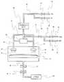
도 3은 본 발명의 일 실시 예에 따른 반도체 제조설비의 개략적인 구성도3 is a schematic configuration diagram of a semiconductor manufacturing apparatus according to an embodiment of the present invention;
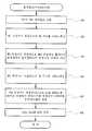
도 4는 본 발명의 일 실시 예에 따른 원격플라즈마 발생에 의한 반도체제조설비의 세정을 위한 흐름도 4 is a flowchart for cleaning a semiconductor manufacturing equipment by remote plasma generation according to an embodiment of the present invention.
* 도면의 주요부분에 대한 부호의 설명 * Explanation of symbols on the main parts of the drawings
10: 프로세스챔버 12: 웨이퍼 척10: process chamber 12: wafer chuck
14: 웨이퍼 16: 메인공정가스 공급관14: wafer 16: main process gas supply pipe
18, 24, 26:제1 내지 제3 에어밸브 20, 22: 제1 및 제2 공정가스 공급관18, 24, 26: first to
28: 가스분배 매니폴드 30: 샤워헤드28: gas distribution manifold 30: shower head
32: 분기관 34: 플라즈마 공급라인32: branch pipe 34: plasma supply line
36: 원격플라즈마 발생기 38: 세정가스 공급라인36: remote plasma generator 38: cleaning gas supply line
40, 42: 제1 및 제2 세정가스 공급관 44, 46: 제4 및 제 5에어밸브40, 42: first and second cleaning
50: 공정가스 배출라인 52: 배출라인50: process gas discharge line 52: discharge line
54: 고진공밸브 56: 진공펌프54: high vacuum valve 56: vacuum pump
본 발명은 반도체 제조설비의 리모트 플라즈마를 이용한 세정방법에 관한 것으로, 특히 PEOX공정을 진행할 시 파티클이 발생되지 않도록 하기 위해 리모트플라즈마를 이용하여 세정하는 PEOX공정을 진행하는 반도체 제조설비의 리모트 플라즈마를 이용한 세정방법에 관한 것이다.The present invention relates to a cleaning method using a remote plasma of a semiconductor manufacturing equipment, and in particular, using a remote plasma of a semiconductor manufacturing equipment performing a PEOX process for cleaning by using a remote plasma in order to prevent particles from being generated during the PEOX process. It relates to a cleaning method.
집적 회로와 같은 반도체 제품들의 제조는 때때로 실리콘 웨이퍼와 같은 기판상에 층들의 형성을 수반한다. 층들이 종종 다른 물질들을 포함함에 따라, 증착 프로세스를 위한 다양한 기술들이 개발되어 왔다. 예를 들어, 금속층이 증착되어 전도성의 인터커넥트를 형성하도록 패턴되거나, 절연층이 한 도전층을 다른 도전층으로부터 전기적으로 절연시키도록 형성될 수 있다. 절연 물질들과 다른 물질들의 층들을 형성하기 위해 사용된 일부 타입의 층 형성 프로세스가 CVD 프로세스이다.The manufacture of semiconductor products such as integrated circuits sometimes involves the formation of layers on a substrate such as a silicon wafer. As the layers often include other materials, various techniques have been developed for the deposition process. For example, a metal layer may be deposited to pattern to form a conductive interconnect, or an insulating layer may be formed to electrically insulate one conductive layer from another. Some type of layer forming process used to form layers of insulating materials and other materials is a CVD process.
화학 기상 증착 프로세스들은, 전자기 에너지가 프리커서(precursor) 가스 또는 증기를 더 반응성의 플라즈마로 변형시키기 위하여 적어도 하나의 프리커서 가스 또는 증기에 인가되는 플라즈마 강화 CVD(" PECVD" ) 프로세스들뿐 아니라, 프리커서 가스 또는 증기가 기판의 가열된 표면에 대응하여 반응하는 열 증착 프로세스들을 포함한다. 플라즈마를 형성하는 것은 막을 형성하는데 필요한 온도를 낮추거나 형성 속도를 증가시킬 수 있다. 따라서, 플라즈마 강화 프로세스는 많은 응용들에서 바람직하다.Chemical vapor deposition processes, as well as plasma enhanced CVD (“PECVD”) processes, in which electromagnetic energy is applied to at least one precursor gas or vapor to transform the precursor gas or vapor into a more reactive plasma, Thermal deposition processes in which the precursor gas or vapor reacts corresponding to the heated surface of the substrate. Forming the plasma may lower the temperature or increase the rate of formation necessary to form the film. Thus, plasma intensification processes are desirable in many applications.
기판상에 층이 형성될 때, 일부 물질은 통상적으로 증착 챔버의 벽들상 및 증착 시스템의 다른 구성 요소들에도 역시 찌꺼기로서 증착된다. 챔버의 벽들상의 물질은, 찌꺼기가 쌓이고 미립자 오염의 소스가 될 수 있기 때문에 일반적으로 바람직하지 못하다. 챔버 내부로부터 찌꺼기를 제거하기 위해 몇 가지 세척 과정들이 개발되었다. " 습식세척(wet-clean)" 으로 알려진 한 타입의 과정은 증착 챔버를 부분적으로 분해하고 적당한 세척액으로 표면들을 닦아줌으로써 수행된다. 다른 타입의 세척 프로세스들은 챔버 배기 시스템에 의해 제거될 수 있는 휘발성 생성물로 찌꺼기를 변환함에의해 찌꺼기를 제거하는 데에 플라즈마를 사용한다. 이러한 프로세스들은 " 건식세척(dry-clean)" 으로 알려져 있다.When a layer is formed on a substrate, some material is typically deposited as debris on the walls of the deposition chamber as well as other components of the deposition system. The material on the walls of the chamber is generally undesirable because it builds up debris and can be a source of particulate contamination. Several cleaning procedures have been developed to remove debris from inside the chamber. One type of process known as "wet-clean" is performed by partially disassembling the deposition chamber and wiping the surfaces with a suitable cleaning solution. Other types of cleaning processes use plasma to remove the debris by converting the debris into volatile products that can be removed by the chamber exhaust system. These processes are known as "dry-clean".
플라즈마 건식세척에는 두 가지 일반적인 타입들이 있다. 한 타입은 프로세싱 챔버 내부에서, 또는 인시튜(in situ)로 플라즈마를 형성한다. 다른 타입은 원격 플라즈마 발생기에 플라즈마를 형성하고, 그 다음 프로세싱 챔버로 플라즈마를 흘려 보낸다. 그러한 원격 플라즈마 세척 프로세스는 인시튜 플라즈마 시스템을 가지지 않은 증착 시스템에 건식세척 능력을 제공하는 것과 같은 몇 가지 이점을 제공한다. 더욱이, 원격 플라즈마 시스템은 세척 플라즈마 프리커서 가스 또는 증기 들을 플라즈마로 변환하는데 더 능률적일 수 있고, 챔버 외부에서 플라즈마를 형성하는 것은 플라즈마가열 및 스퍼터링 효과와 같은 플라즈마 형성 프로세스의 바람직하지 않은 잠재적인 부산물들로부터 챔버 내부를 보호한다.There are two general types of plasma dry cleaning. One type forms a plasma inside the processing chamber or in situ. Another type forms a plasma in a remote plasma generator and then flows the plasma into the processing chamber. Such remote plasma cleaning processes provide several advantages, such as providing dry cleaning capabilities for deposition systems that do not have an in-situ plasma system. Moreover, remote plasma systems can be more efficient at converting the cleaning plasma precursor gas or vapors into plasma, and forming the plasma outside the chamber is undesirable potential byproducts of the plasma forming process such as plasma heating and sputtering effects. To protect the inside of the chamber from
이러한 원격플라즈마 시스템을 세척하는 기술이 미합중국 특허 US 6,29,297호에 개시되어 있다. 미합중국 특허 US 6,29,297호는 세척 플라즈마 및 희석물 가스의 혼합물을 챔버내로 흘려보내기 전에 원격 플라즈마 발생기에 형성된 세척플라즈마를 희석함으로써 증착 챔버를 보다 완전하고 균일하며 빠르게 세척한다. 특정 실시예에서, 산화 실리콘 막을 기판상에 증착시키기 위해 사용되는 증착 시스템은 그 후에 증착 챔버로 도입되기 전에 이원자 질소 가스(N2)로 희석되는, 원격 형성된 삼불화 질소(NF3) 플라즈마의 혼합물을 사용하여 세척된다. PECVD 시스템은, 예를 들어, 테트라에틸오르토시레인 (tetraethylorthosilane;" TEOS" ) 또는 실란을 증착 가스로써 사용한다. 원격 마이크로웨이브 플라즈마 발생기는, 가스 인입구 노즐을 통하여 증착 챔버로 혼합물을 흘려보내기 전에, 희석되지 않은 NF3 또는 다른 세척 또는 에칭 프리커서 가스를 N2 또는 다른 일반적으로 비반응성인 희석물 가스로 희석되는 세척 플라즈마로 효율적으로 변환시킨다. 세척 프로세스는 200mm 웨이퍼들과 함께 사용되는 증착 시스템들 상에서 사용될 수 있고, 300mm 증착 시스템들 상에서 사용되도록 비율조정될 수 있다. 희석물의 흐름을 변화시키는 것은 시스템의 에칭 프로파일을 변화시키고 에칭 속도를 증가시키며 챔버 세척에 필요한 시간을 감소시킨다.Techniques for cleaning such remote plasma systems are disclosed in US Pat. No. 6,29,297. US Pat. No. 6,29,297 cleans the deposition chamber more completely, uniformly and quickly by diluting the cleaning plasma formed in the remote plasma generator before flowing the mixture of cleaning plasma and diluent gas into the chamber. In certain embodiments, the deposition system used to deposit a silicon oxide film on a substrate then uses a mixture of remotely formed nitrogen trifluoride (NF 3) plasma, which is then diluted with diatomic nitrogen gas (N 2) before being introduced into the deposition chamber. By washing. PECVD systems use, for example, tetraethylorthosilane (“TEOS”) or silane as the deposition gas. The remote microwave plasma generator is a cleaning plasma in which undiluted NF3 or other cleaning or etching precursor gas is diluted with N2 or other generally non-reactive diluent gas before flowing the mixture through the gas inlet nozzle into the deposition chamber. Convert efficiently to The cleaning process can be used on deposition systems used with 200 mm wafers and can be scaled to be used on 300 mm deposition systems. Changing the dilution flow changes the etch profile of the system, increases the etch rate and reduces the time required for chamber cleaning.
프로세스 웨이퍼는 원격 플라즈마 발생기에서 발생되고 그 후 웨이퍼를 에칭 하기 위해 챔버내로 도입되기 전에 N2로 희석되는 에칭 플라즈마를 사용하여 에칭된다. 희석물 흐름은 웨이퍼를 가로지르는 에칭 프로파일 및 /또는 에칭 속도를 제어하기 위하여 선택될 수 있는 반면, 에칭 플라즈마 프리커서 흐름은 플라즈마 변환 효율을 최적화하거나 및/또는 프리커서 흐름을 보존하기 위하여 선택된다.Process wafers are etched using an etch plasma that is generated in a remote plasma generator and then diluted with N2 before being introduced into the chamber to etch the wafer. Diluent flow may be selected to control the etch profile and / or etch rate across the wafer, while the etch plasma precursor flow is selected to optimize plasma conversion efficiency and / or to preserve the precursor flow.
예시적인 기판 프로세싱을 수행하기 위한 하나의 적당한 CVD 장치가 도 1에 나타나 있으며, 도 1은 챔버 벽(15a) 챔버 리드(lid) 어셈블리(15b)를 포함하는 진공 챔버 또는 프로세싱 챔버(15)를 가지는 CVD 시스템(10)의 간략도이다.One suitable CVD apparatus for performing exemplary substrate processing is shown in FIG. 1, which has a vacuum chamber or
CVD 시스템(10)은 프로세스 가스들을 프로세싱 챔버내의 받침대(12)상에 놓인 기판(미도시)으로 분산시키기 위한 가스 분배 " 매니폴드" (manifold;11)를 포함한다. 받침대는 알루미늄, 알루미나 또는 질화 알루미늄과 같은 세라믹, 또는 다른 물질들 및 물질들의 결합들로 만들어질 수 있다. 받침대는 프로세싱동안 기판을 가열할 내장된 저항 히터(미도시) 또는 고주파(RF) 전극 및/또는 서셉터와 같은 다른 구조들을 포함할 수 있다. 내장된 저항 히터를 위해서 다양한 구성들이 사용될 수 있다. 바람직한 실시예에서, 단일 엘리먼트는 평행한 동심원들의 형태로 두개의 완전한 회전을 만든다. 외부 전원(미도시)까지 받침대 하부를 통과하는 스템(12c)내의 전선들을 통하여 가열 엘리먼트로 전력이 공급된다.The
프로세싱의 동안, 기판(예:반도체 웨이퍼)은 받침대(12)의 평평한(또는 약간 볼록한) 표면(12a)상에 위치된다. 받침대는 하부 로딩/오프-로딩 위치와 매니폴드(11)와 가까이 인접하는 상부 프로세싱 위치(점선(14)에 의해 표시) 사이에서 제어 가능하게 이동할 수 있다. 중심판(미도시)은 받침대의 위치에 관한 정보를 제공 하는 센서들을 가진다.During processing, the substrate (eg, semiconductor wafer) is placed on the flat (or slightly convex) surface 12a of the
도 1에서는 원형 가스 분배(11)의 뚫린 구멍들을 통하여 챔버(15)내로 가스들이 유입된다. 보다 상세하게는, 증착 프로세스 가스들은 인입구 매니폴드(11), 관통된 블록커(blocker) 판(42), 그 다음 가스 분배 면판(11)의 구멍을 통하여 챔버내로 유입된다.In FIG. 1, gases are introduced into the
가스 패널(6)은 혼합 블록(9)으로의 가스 공급 라인들(8)을 통하여 가스를 매니폴드(11)로 공급하는 가스 소스들 7a-d를 포함하는데 가스들은 혼합블록에서 블록커판(42) 및 면판(13a)을 통하여 챔버(15)로 흐르기전에 혼합된다.The gas panel 6 comprises gas sources 7a-d which supply gas to the manifold 11 via gas supply lines 8 to the mixing block 9, the gases being
각 프로세스 가스를 위한 공급 라인은 전형적으로 가스 분배 통로를 따라 여러 포인트들에 있는 안전 차단 밸브들(미도시)을 포함하는데, 그것은 가스의 흐름을 국부 또는 원격 제어를 통하여 자동 또는 수동으로 차단한다. 가스 패널은 또한 매스 흐름 제어기들(미도시) 또는 공급 라인을 통하여 챔버로 흐르는 가스의 흐름을 제어하는 다른 디바이스들을 포함한다. 당업자들은 도 1에서 나타난 구성은 단지 예시적인 것이고, 예를 들어, 더 많거나 적은 가스 소스들이 특정의 응용을 위해 사용될 수 있으며 구성에 대한 다른 조정들도 적절할 수 있다는 것을 이해한다.The supply line for each process gas typically includes safety shutoff valves (not shown) at several points along the gas distribution passageway, which automatically or manually shut off the flow of gas via local or remote control. The gas panel also includes mass flow controllers (not shown) or other devices that control the flow of gas into the chamber through the supply line. Those skilled in the art understand that the configuration shown in FIG. 1 is merely exemplary, and that, for example, more or fewer gas sources may be used for a particular application and other adjustments to the configuration may be appropriate.
CVD 시스템(10)은 열 CVD 프로세스 또는 플라즈마-강화 CVD(PECVD) 프로세스를 수행하도록 구성될 수 있다. PECVD 프로세스들은 인시튜에서 형성된 플라즈마 또는 원격 플라즈마 발생기(27)에서 형성된 플라즈마를 사용할 수 있다. 인시튜 PECVD 프로세스에서, RF 전원(44)은, 면판(13a)과 받침대의 표면(12a) 사이의 원통형 영역 내에 플라즈마를 형성하기 위해, 가스 분배 면판(13a)과 받침대(12) 사이 에 RF 전력과 같은 전력을 인가한다.(이 영역은 여기에서 " 반응 영역" 으로 언급될 것이다.) 플라즈마의 구성 성분들은 반응하여 받침대상에서 지지되는 반도체 웨이퍼 표면상에 목적하는 막을 형성한다.
RF 전원(44)은 13.56MHz의 높은 RF 주파수(RF1) 및/또는 360KHz의 낮은 RF 주파수(RF2)에서 전력을 공급할 수 있는 혼합 주파수 공급기이다. 플라즈마를 형성하기 위해 혼합된 높고 낮은 주파수들을 사용하는 것은 진공 챔버(15)로 유입되는 반응 종의 분해를 강화한다.
원격 플라즈마 프로세스에서, 가스 소스(7a)로 부터의 프로세스 가스는 원격 플라즈마 발생기(27)로 공급된다. 마이크로웨이브 소스(28)는 가스 분배 면판(13a)를 통하여 챔버내로 흐르는 플라즈마를 형성하기 위하여 마이크로웨이브 에너지로 플라즈마 챔버(29)를 조사(irradiate)한다. 원격 플라즈마 발생기에서 플라즈마가 형성될 때, 고 에너지 포톤 및 열과 같은 플라즈마 형성의 전형적인 부산물은 프로세스 웨이퍼나 증착 챔버 내부에 직접적으로 영향을 미치지는 않는다. 더욱이, 일부 플라즈마 프리커서 가스들은, 인시튜 플라즈마 시스템의 더 낮은 주파수보다 원격 마이크로웨이브 플라즈마 발생기에서 보다 효율적으로 분해된다.In the remote plasma process, process gas from the gas source 7a is supplied to the remote plasma generator 27. The
열처리에서 프로세스 가스 혼합물은, 반응을 위한 열 에너지를 공급하기 위하여 가열되는 받침대(12)상에 지지되는 반도체 웨이퍼의 표면상에 바람직한 막들을 증착시키기 위하여 반응한다. 웨이퍼상에 바람직한 막의 형성을 더 촉진 또는 제어하기 위하여 플라즈마 강화 CVD 프로세스들이 웨이퍼를 가열할 수 있다고 또는 웨이퍼가 가열될 수 있다고 이해된다.In the heat treatment the process gas mixture reacts to deposit the desired films on the surface of the semiconductor wafer supported on the
배기 통로(23) 및 차단 밸브(24)와 같은 주변 구조들 및 증착 챔버의 벽들의 온도는 챔버 벽들 내의 채널들(미도시)을 통한 열교환액의 순환에 의해 또한 제어될 수 있다. 열교환액은 챔버벽들을 바람직한 효과에 따라 가열하거나 냉각하기 위하여 사용될 수 있다. 예를 들어, 원 위치 플라즈마 프로세스의 동안 차가운 액체가 시스템으로부터 열을 제거하거나 챔버의 벽들상에 증착 생성물들의 형성을 제한하기 위해 사용될 수 있는 반면, 열 증착 프로세스 동안 뜨거운 액체는 고른 열 경도를 유지하도록 도울 수 있다. 가스 분배 매니폴드(11)는 열 교환 통로들(18)을 가진다. 전형적인 열교환액들은 수계(water-based) 에틸렌글리콜 혼합물, 유계(oil-based) 열전달 액체들 또는 유사한 액체들이다. " 열교환자" 에 의한 가열로 언급되는 이 가열은 바람직하지 않은 반응 산물들의 응축을 감소시키거나 제거하고, 프로세스 가스들의 휘발성 산물들 및, 차가운 진공 통로들의 벽들상에 응축되고 가스 흐름이 없는 기간 동안 프로세싱 챔버내로 되돌아간다면 프로세스를 오염시킬 수 있는, 다른 오염물들의 제거를 개선시킨다.The surrounding structures such as the exhaust passage 23 and the
반응 부산물들을 포함하는, 층에 증착되지 않는 가스 혼합물의 나머지는 진공 펌프(30)에 의해 챔버로부터 배기된다.The remainder of the gas mixture that is not deposited in the layer, including the reaction byproducts, is evacuated from the chamber by the
특히, 가스들은 반응 영역을 둘러싸는 환형(annular) 슬롯형 오리피스(orifice)(16)을 통하여 고리 모양 배기 플레넘(17)으로 배기된다. 고리 모양 슬롯형 구멍(16) 및 플레넘(17)은 챔버의 원통형 측면벽(15a)(벽상의 상부 절연 라이닝을 포함함)의 상부와 원통형 챔버 리드(20)의 하부 사이의 틈으로 정의된다. 슬롯 구멍(16) 및 플레넘(17)의 원형대칭 및 균일성은 웨이퍼상에 균일한 막을 증착 시키기 위하여 웨이퍼상으로의 본질적으로 균일한 프로세스 가스들의 흐름을 만든다.In particular, the gases are exhausted into an annular exhaust plenum 17 through an annular slotted
배기 플레넘(17)으로부터, 가스들은 배기 플레넘(17)의 측면 연장 부분(21)의 아래로, 뷰잉 포트(viewing port)(미도시)를 지나고, (본체가 하부 챔버벽(15a)과 통합된)진공 차단 밸브(24)를 지나며 배기 출구(25)내로 흐른다. 배기출구(25) 및 포어라인(foreline;31) 사이의 스로틀 밸브(32;throttle valve)는 챔버내의 선택된 압력 및/또는 가스흐름을 유지하도록 조정될 수 있다. 일부 프로세스들이나 프로세스 단계에서, 스로틀 밸브의 위치는 압력 센서(미도시)로부터 제어기(34)로의 피드백 신호에 따라 정해진다. 다른 프로세스들이나 프로세스 단계에서는, 피드백 루프는 디스에이블되고 스로틀 밸브는 고정된 위치로 정해진다. 스로틀 밸브를 완전히 여는 것에 의해 최대 펌핑 속도가 제공된다.From the exhaust plenum 17, gases pass through a viewing port (not shown) below the lateral extension 21 of the exhaust plenum 17 (the body is connected to the lower chamber wall 15a). Flows into the exhaust outlet 25 through the integrated
그러므로, 진공 펌프가 일정 속도로 작동하는 동안, 챔버상의 배기 끌어당김은 스로틀 밸브로 조정될 수 있다. 모터(32)에 의해 동작되는 승강 메커니즘은 히터 받침대 어셈블리를 상승시키거나 하강시킨다. 받침대가 하강될 때, 웨이퍼 승강핀들(12b)은 승강핀판(33)과 접하고 웨이퍼를 받침대의 표면(12a)으로부터 들어올린다. 웨이퍼 핀들(12b)은 웨이퍼들을 챔버 측면의 삽입/제거 구멍(26)을 통하여 이송하기에 적당한 높이에 위치한다. 로보트 블레이드(미도시)가 챔버들 사이 또는 챔버 및 웨이퍼 카세트 사이에서 웨이퍼들을 이송할 수 있다. 웨이퍼를 탑재한 후, 모터는 웨이퍼를 선택된 프로세싱 위치로 들어올린다.Therefore, while the vacuum pump is operating at a constant speed, the exhaust attraction on the chamber can be adjusted with the throttle valve. An elevating mechanism operated by the
시스템 제어기(34)는 다양한 서브시스템들 및 증착 시스템(10)의 메커니즘들 을 제어한다. 웨이퍼 위치 시스템, 가스공급 시스템, 챔버 압력 시스템, 가열 시스템들 및 플라즈마 시스템들은 컴퓨터 판독 가능 메모리(38)에 저장된 프로그램(70)에 따라 시스템 제어기(34)에 의해 제어된다. 시스템 제어기로 및 그로부터의 신호들은 제어 라인들(36)을 통해 전달되며, 제어 라인들은 단순화를 위해 그 일부만이 도시된다. 제어기(34)는, 제어기(34)의 제어하의 적절한 모터들에 의해 움직이는 받침대(12) 및 스로틀 밸브(32)와 같은 이동 가능 기계 어셈블리들의 위치를 결정하기 위해, 광센서들과 같은 센서들로부터의 피드백 신호들에 의존한다.
메모리(38)는 하드 드라이브, 읽기 전용 메모리, 임의 접근 메모리, 플로피 디스크 드라이브 또는 다른 적절한 저장 장치를 포함할 수 있다. 프로세서(37)는 싱글 보드 컴퓨터(SBC), 아날로그 및 디지털 입출력 보드들, 인터페이스 보드들 및 스텝 모터 제어기 보드들을 포함한다. CVD 시스템(10)의 다양한 부분들은, 보드와 카드 케이지 및 커넥터 크기들 및 타입들을 정의하는 베사 모듈러 유럽(Versa Modular European;VME) 규격에 따른다. VME 규격은 또한 16비트데이터 버스 및 24비트 어드레스 버스를 가지는 것과 같은 버스 구조를 정의한다.
시스템 제어기는 시스템 제어 소프트웨어를 실행하는데, 이는 범용 증착 시스템을 특정 증착 시스템으로 구성하기 위해 컴퓨터가 판독할 수 있는 메모리(38)내에 저장된 컴퓨터 프로그램(70)이다. 바람직하게는, 메모리(38)는 하드디스크 드라이브이나, 메모리(38)는 다른 종류의 메모리일 수도 있다.The system controller executes system control software, which is a computer program 70 stored in a computer
컴퓨터 프로그램은, 타이밍, 가스들의 혼합, 챔버 압력, 챔버 온도, RF 전력 레벨, 받침대 위치 및 특정 프로세스의 다른 파라미터들을 명령하는, 명령들의 집 합을 포함한다. 예를 들어, 플로피 디스크 또는 다른 적절한 드라이브를 포함하는, 다른 메모리 디바이스들상에 저장된 다른 컴퓨터 프로그램들도 제어기(34)를 작동시키기 위하여 또한 사용될 수 있다.The computer program includes a set of instructions that instructs timing, mixing of gases, chamber pressure, chamber temperature, RF power level, pedestal position and other parameters of a particular process. Other computer programs stored on other memory devices, including, for example, floppy disks or other suitable drives, may also be used to operate the
이와 같은 시스템을 이용하여 PETEOS공정을 적용할 경우 문제가 없었으나 PEOX공정을 적용할 경우 SiH4, N2O, N2가스를 사용하게 되어 원격플라즈마 크린시 사용되는 NF3와 공정 시 사용되어 잔류하는 SiH4가 반응하여 파티클 오염이 발생하여 공정을 적용할 수 없는 문제가 있었다.When applying PETEOS process using this system, there was no problem, but when applying PEOX process, SiH4, N2O, N2 gas is used, and NF3 used in remote plasma clean and SiH4 remaining in the process react. Particle contamination occurred and there was a problem that the process could not be applied.
NOVELLUS사(社)설비에서 PEOX공정을 완료한 후 원격플라즈마 크린(RPC: Romote Plasma Clean)을 실시한 후 다시 PEOX공정을 진행하였을 경우 50매진행시까지 도 2와 같이 파티클이 발생되었다.After completing the PEOX process at the NOVELLUS company, the remote plasma clean (RPC: Romote Plasma Clean) was performed, and when the PEOX process was performed again, particles were generated as shown in FIG.
따라서 본 발명의 목적은 상기와 같은 문제를 해결하기 위해 원격플라즈마 크린 후 PEOX공정 진행 시 파티클에 의한 오염을 방지할 수 있는 반도체 제조설비 및 그 반도체 제조설비의 리모트 플라즈마를 이용한 세정방법을 제공함에 있다.Accordingly, an object of the present invention is to provide a semiconductor manufacturing equipment and a cleaning method using a remote plasma of the semiconductor manufacturing equipment that can prevent contamination by particles during the PEOX process after the remote plasma cleaning to solve the above problems. .
상기 목적을 달성하기 위한 PEOX공정을 진행하기 위한 반도체 제조설비는, SiH4, N2O가스를 공급받아 PEOX공정을 진행하기 위한 프로세스챔버와, 공정가스를 공급하기 위한 통로를 형성하는 메인공정가스 공급라인과, 상기 메인공정가스 공급 라인 상에 설치되어 제1 공정가스(SiH4)와 제2 공정가스(N2O)를 자동으로 공급하거나 차단하는 에어밸브와, 상기 메인공정가스 공급라인 통해 유입된 공정가스를 분산시키기 위한 가스분배 매니폴드와, 상기 가스분배 매니폴드로부터 분산되어 유입된 공정가스를 상기 프로세스챔버내부로 분사하는 샤워헤드와, 소정의 공정가스가 유입될 때 리액터에 의해 원격 플라즈마를 발생하는 원격플라즈마 발생기와, 상기 원격플라즈마 발생기로부터 발생된 NF3 또는 Ar 플라즈마가스를 상기 프로세스 챔버로 공급하기 위한 통로를 형성하는 원격플라즈마 공급라인과, 상기 프로세스챔버의 하부에 연결되어 공정가스를 배출하기 위한 공정가스 배출라인을 포함함을 특징으로 한다.The semiconductor manufacturing equipment for proceeding the PEOX process to achieve the above object, the main process gas supply line for forming a process chamber for supplying the process gas, the process chamber for supplying the process gas and the supply of SiH4, N2O gas and And an air valve installed on the main process gas supply line to automatically supply or block a first process gas (SiH4) and a second process gas (N2O), and a process gas introduced through the main process gas supply line. A gas distribution manifold, a shower head for injecting the process gas dispersed from the gas distribution manifold into the process chamber, and a remote plasma generating a remote plasma by a reactor when a predetermined process gas is introduced. Generator and cylinder for supplying NF3 or Ar plasma gas generated from the remote plasma generator to the process chamber , And a remote plasma supply line to form a connected to the lower portion of the process chambers is characterized in that it comprises a process gas discharge line for discharging the process gas.
상기 원격플라즈마 발생기는 NF3가스를 공급받아 플라즈마를 발생하여 상기 리액터를 세정하는 것을 특징으로 한다.The remote plasma generator is supplied with NF 3 gas to generate a plasma to clean the reactor.
상기 원격플라즈마 발생기는 상기 리액터를 세정한 후 Ar가스를 공급받아 플라즈마를 발생하여 상기 리액터와 상기 프로세스챔버에 잔류하는 상기 NH3가스를 제거함을 특징으로 한다.The remote plasma generator cleans the reactor and is supplied with Ar gas to generate plasma to remove the NH 3 gas remaining in the reactor and the process chamber.
상기 목적을 달성하기 위한 본 발명에 따르면, 원격플라즈마 발생기를 구비한 반도체 제조설비의 리모트 플라즈마를 이용한 세정방법은, PEOX공정이 완료된 후 SiH4 아웃렛 라인을 오픈시켜 N2가스를 공급하여 프로세스챔버를 퍼지시키는 단계와, 상기 N2가스가 퍼지되는 상태에서 상기 원격플라즈마 발생기로 NF3가스를 설정시간 동안 공급하고 플라즈마를 형성하여 상기 원격플라즈마 발생기의 리액터를 세정하는 단계와, 상기 원격플라즈마 발생기의 리액터 세정을 완료한 후 상기 SiH4 공급라인을 오픈시키고 N2가스를 공급하여 상기 프로세스챔버를 통해 퍼지시키는 단계와, 상기 N2가스로 상기 프로세스챔버를 통해 퍼지시키는 상태에서 상기 원격플라즈마 발생기로 Ar을 공급하고 플라즈마를 발생하여 상기 원격플라즈마 발생기와 상기 프로세스챔버에 잔류하는 NF3가스를 제거하는 단계와, 상기 NF3가스를 제거한 후 풀 플러쉬를 설정된 횟수만큼 진행하여 상기 프로세스챔버에 잔류하는 공정가스를 제거하는 단계로 이루어짐을 특징으로 한다.According to the present invention for achieving the above object, the cleaning method using a remote plasma of the semiconductor manufacturing equipment having a remote plasma generator, after the PEOX process is completed by opening the SiH4 outlet line to supply the N2 gas to purge the process chamber And cleaning the reactor of the remote plasma generator by supplying NF3 gas to the remote plasma generator for a predetermined time while the N2 gas is purged, forming a plasma, and completing the reactor cleaning of the remote plasma generator. And opening the SiH4 supply line and supplying N2 gas to purge through the process chamber, and supplying Ar to the remote plasma generator in the state of purging the N2 gas through the process chamber and generating a plasma. Remote Plasma Generator and Process Chamber Is a made of an step of removing residual NF3 gas and comprising the steps of the process proceeds as set number of full flushing, remove the NF3 gas to remove the process gas remaining in the process chamber characteristics.
상기 풀 플러쉬의 설정된 횟수는 10회임을 특징으로 한다.The set number of times of the full flush is characterized in that 10 times.
상기 Ar가스는 1500cc의 유량으로 120초동안 공급함을 특징으로 한다.The Ar gas is supplied for 120 seconds at a flow rate of 1500 cc.
상기 풀 풀러쉬는 N2가스를 9000cc의 유량으로 333초동안 SiH4 공급라인과 N2O 공급라인으로 교대로 공급함을 특징으로 한다.The full full rush is characterized in that the N2 gas is alternately supplied to the SiH4 supply line and the N2O supply line for 333 seconds at a flow rate of 9000 cc.
상기 NF3가스 세정 후 상기 SiH4 공급라인으로 공급되는 상기 N2가스는 상기 SiH4 공급라인으로 상기 NF3가 역류하지 않도록 함을 특징으로 한다.The N2 gas supplied to the SiH4 supply line after the NF3 gas cleaning is characterized in that the NF3 does not flow back to the SiH4 supply line.
이하 본 발명에 따른 바람직한 실시 예를 첨부한 도면을 참조하여 상세히 설명한다. 그리고 본 발명을 설명함에 있어서, 관련된 공지 기능 혹은 구성에 대한 구체적인 설명이 본 발명의 요지를 불필요하게 흐릴 수 있다고 판단되는 경우 그 상세한 설명을 생략한다.Hereinafter, exemplary embodiments of the present invention will be described in detail with reference to the accompanying drawings. In the following description of the present invention, if it is determined that a detailed description of a related known function or configuration may unnecessarily obscure the subject matter of the present invention, the detailed description thereof will be omitted.
도 3은 본 발명의 일 실시 예에 따른 반도체 제조설비의 개략적인 구성도이다.3 is a schematic diagram of a semiconductor manufacturing apparatus according to an embodiment of the present invention.
SiH4, N2O가스를 공급받아 PEOX공정을 진행하기 위한 프로세스챔버(10)와, 상기 프로세스 챔버(10)내에 설치된 웨이퍼 척(12)과, 상기 웨이퍼 척(12) 상에 놓 여지는 웨이퍼(14)와, 공정가스를 공급하기 위한 통로를 형성하는 메인공정가스 공급관(16)과, 상기 메인공정가스 공급관(16) 상에 설치되어 공정가스를 자동으로 공급하거나 차단하는 제1 에어밸브(18)와, 상기 메인공정가스 공급관(16)과 연통되어 제1 공정가스(SiH4)를 공급하기 위한 통로를 형성하는 제1 공정가스 공급관(22)과, 상기 메인공정가스 공급관(16)과 연통되어 제2 공정가스(N2O)를 공급하기 위한 통로를 형성하는 제2 공정가스 공급관(22)과, 상기 제1 공정가스 공급관(20) 상에 설치되어 제1 공정가스를 공급하거나 차단하는 제2 에어밸브(24)와, 상기 제2 공정가스 공급관(22) 상에 설치되어 제2 공정가스를 공급하거나 차단하는 제3 에어밸브(26)와, 상기 메인공정가스 공급관(16)을 통해 유입된 공정가스를 분산시키기 위한 가스분배 매니폴드(28)와, 상기 가스분배 매니폴드(28)에 연통되어 상기 분산된 가스를 상기 프로세스챔버(10)로 공급하기 위한 통로를 형성하는 분기관(32)과, 상기 가스분배 매니폴드(28)로부터 분산되어 상기 분기관(32)를 통해 유입된 공정가스를 프로세스챔버(10)내부로 분사하는 샤워헤드(30)와, 상기 분기관(32)에 연통되어 원격 플라즈마를 프로세스챔버(10)로 공급하기 위한 통로를 형성하는 플라즈마 공급라인(34)과, 공정가스가 유입될 때 원격 플라즈마를 발생하는 원격플라즈마 발생기(36)와, 상기 원격플라즈마 발생기(36)에 연결되어 상기 원격플라즈마 발생기(36)로부터 발생된 NF3 또는 Ar가스를 공급하기 위한 통로를 형성하는 세정가스 공급라인(38)과, 상기 세정가스 공급라인(38)에 연통되어 제1 세정가스(NF3)를 공급하기 위한 통로를 형성하는 제1 세정가스 공급관(40)과, 상기 세정가스 공급라인(38)에 연통되어 제2 세정가스(Ar)를 공급하기 위한 통로를 형성하는 제2 세정가 스 공급관(42)과, 상기 제1 세정가스 공급관(40) 상에 설치되어 제1 세정가스를 공급하거나 차단하는 제4 에어밸브(44)와, 상기 제2 세정가스 공급관(42) 상에 설치되어 제2 세정가스를 공급하거나 차단하는 제5 에어밸브(46)와, 상기 프로세스챔버(10)의 하부에 연결되어 공정가스를 배출하기 위한 공정가스 배출라인(50)과, 상기 공정가스 배출라인(50) 상에 설치되어 프로세스챔버(10)내의 선택된 압력 및/또는 가스흐름을 유지하도록 조절하기 위한 스로틀 밸브(throttle valve)(52)와, 상기 프로세스챔버(10)와 상기 진공펌프(56)간을 차단하기 위한 고진공밸브(Hi-Vacuum Valve)(54)와, 상기 프로세스쳄버(10)를 진공으로 형성시킬 수 있도록 펌핑동작을 수행하는 진공펌프(56)로 구성되어 있다.The
도 4는 본 발명의 일 실시 예에 따른 원격플라즈마 발생에 의한 반도체제조설비의 세정을 위한 흐름도이다.4 is a flowchart for cleaning a semiconductor manufacturing apparatus by remote plasma generation according to an embodiment of the present invention.
상술한 도 3 내지 도 4를 참조하여 본 발명의 바람직한 실시 예의 동작을 상세히 설명한다.3 to 4 will be described in detail the operation of the preferred embodiment of the present invention.
제1 내지 제3 에어밸브(18, 24, 26)가 오픈되고 SiH4, N2O가스가 메인공정가스 공급관(16)을 통해 매니폴드(28)로 유입되면 가스분배 매니폴드(28)에서 가스가 분산되어 샤워헤드(30)로 유입된다. 이때 상기 샤워헤드(30)는 분기관(32)를 통해 분산된 혼합공정가스를 프로세스챔버(10)의 내부로 분사한다. 상기 프로세스챔버(10)의 내부로 분사된 혼합공정가스는 프로세스 챔버(10)에서 플라즈마로 형성되어 웨이퍼(14)에 증착되어 PEOX공정이 진행된다. 이와 같이 PEOX공정이 진행되고 나서 원격플라즈마 발생기(36)와 프로세스챔버(10)를 주기적으로 세정하여야 한다.When the first to
원격플라즈마 발생기(36)와 프로세스챔버(10)를 세정하는 동작을 도 4를 참조하여 설명한다.The operation of cleaning the
원격플라즈마 크린(Remote Plasma Clean)이 시작되면 101단계에서 도시하지 않는 콘트롤러는 제1 및 제2 에어밸브(18, 24)를 오픈시킨다. 즉, SiH4 아웃렛(Outlet)라인 밸브를 오프시킨다. 그리고 102단계에서 제1 공정가스 공급관(20)을 통해 1500cc가 일정하게 유동되도록 N2가스를 공급한다. 그런 후 103단계에서 제4에어밸브(44)를 오픈시키고 제1 세정가스 공급관(40)을 통해 제1 세정가스인 NF3가스를 원격플라즈마 발생기(36)로 공급하고 RF전원을 공급하여 플라즈마가 발생되도록 하여 원격플라즈마 발생기(36)에 설치된 리액터를 세정한다. 상기 원격플라즈마 발생기(36)에서 리액터를 세정하면서 배출되는 플라즈마는 플라즈마 공급라인(34)을 통해 프로세스챔버(10)로 유입되고, 프로세스챔버(10)로 유입된 NF3가스는 진공펌프(56)의 펌핑에 의해 공정가스 배출라인(50)을 통해 배출된다. 이때 제1 공정가스 공급관(20)을 통해 공급되는 N2가스는 원격플라즈마 발생기(36)로부터 배출되는 NF3가스의 역류를 방지하는 기능을 한다. 원격플라즈마 발생기(36)의 리액터 세정이 완료되면 원격플라즈마 발생기(36)의 동작이 정지된 후 104단계에서 제1 공정가스 공급관(20)을 통해 1500cc가 일정하게 유동되도록 N2가스를 공급한다. 그런 후 105단계에서 제5에어밸브(46)를 오픈시키고 제2 세정가스 공급관(42)을 통해 Ar가스를 1500cc가 일정하게 유지되도록 원격플라즈마 발생기(36)로 120초 동안 공급하고 RF전원을 공급하여 플라즈마가 발생되도록 하여 원격플라즈마 발생기(36)와 프로세스챔버(10)에 잔류하는 NF3가스를 세정한다.When Remote Plasma Clean is started, the controller (not shown) opens the first and
이렇게 원격플라즈마 발생기(36)와 프로세스챔버(10)가 Ar가스에 의한 퍼지가 완료되면 제2에어밸브(24) 및 제5 에어밸브(46)가 클로즈되고 원격플라즈마 발생기(36)의 동작이 정지된다. 그런 후 106단계에서 풀 플러쉬(Full Flush)동작을 10회 진행한다. 풀 플러쉬동작은 제1 및 제2 에어밸브(18, 24)를 오픈시킨상태에서 제1 공정가스 공급관(20)을 통해 N2가스를 9000cc가 유지되도록 333초동안 공급하고 제2 에어밸브(24)를 클로즈시킨다. 그런 후 제3에어밸브(26)를 오픈시키고 제2 공정가스 공급관(22)를 통해 N2가스를 9000cc가 유지되도록 333초동안 공급하고 제3 에어밸브(26)를 클로즈시킨다. 이와 같은 동작을 10회반복하여 메인공정 가스공급관(16)을 통해 프로세스 챔버(10)로 N2가스를 퍼지시키게 되면 프로세스챔버(10)로 유입된 N2가스는 진공펌프(56)의 펌핑에 의해 공정가스 배출라인(50)을 통해 배출되어 프로세스챔버(10)를 세정하게 된다.When the
한편 상기한 설명에서 많은 사항이 구체적으로 기재되어 있으나, 그들은 발명의 범위를 한정하는 것이라기보다는 바람직한 실시예의 예시로서 해석되어야 한다. 따라서 본 발명의 범위는 설명된 실시예에 의하여 정하여 질 것이 아니고 특허 청구범위에 기재된 기술적 사상에 의해 정하여져야 한다.On the other hand, while many matters have been described in detail in the above description, they should be construed as illustrative of preferred embodiments rather than to limit the scope of the invention. Therefore, the scope of the present invention should not be defined by the described embodiments, but should be determined by the technical spirit described in the claims.
상술한 바와 같이 본 발명은 반도체 제조설비의 PEOX공정에서 원격플라즈마 크린(Remote Plasma Clean) 시 사용되는 NF3가스가 프로세스챔버내에 잔류하지 않도록 세정하여 PEOX공정진행 시 웨이퍼에 파티클이 발생하지 않도록 하여 품질불량 을 방지하고, 또한 프로세스 챔버 내부가 NF3에 의한 오염을 방지하여 프로세스챔버의 분해 크리닝을 6개월주기로 연장가능하도록 하여 크리닝을 자주하지 않게 되어 생산성을 향상시킬 수 있는 이점이 있다.As described above, the present invention cleans the NF3 gas used during the Remote Plasma Clean in the PEOX process of the semiconductor manufacturing equipment so that no particles remain on the wafer during the process of the PEOX process. In addition, the inside of the process chamber is prevented from being contaminated by NF3, so that the decomposition cleaning of the process chamber can be extended to a six month period, thereby eliminating frequent cleaning, thereby improving productivity.
Claims (8)
Translated fromKoreanPriority Applications (2)
| Application Number | Priority Date | Filing Date | Title |
|---|---|---|---|
| KR1020060114902AKR100819096B1 (en) | 2006-11-21 | 2006-11-21 | Cleaning Method Using Remote Plasma in Semiconductor Manufacturing Equipment |
| US11/942,761US8025736B2 (en) | 2006-11-21 | 2007-11-20 | Semiconductor device fabrication equipment for performing PEOX process and method including cleaning the equipment with remotely produced plasma |
Applications Claiming Priority (1)
| Application Number | Priority Date | Filing Date | Title |
|---|---|---|---|
| KR1020060114902AKR100819096B1 (en) | 2006-11-21 | 2006-11-21 | Cleaning Method Using Remote Plasma in Semiconductor Manufacturing Equipment |
Publications (1)
| Publication Number | Publication Date |
|---|---|
| KR100819096B1true KR100819096B1 (en) | 2008-04-02 |
Family
ID=39415708
Family Applications (1)
| Application Number | Title | Priority Date | Filing Date |
|---|---|---|---|
| KR1020060114902AActiveKR100819096B1 (en) | 2006-11-21 | 2006-11-21 | Cleaning Method Using Remote Plasma in Semiconductor Manufacturing Equipment |
Country Status (2)
| Country | Link |
|---|---|
| US (1) | US8025736B2 (en) |
| KR (1) | KR100819096B1 (en) |
Cited By (2)
| Publication number | Priority date | Publication date | Assignee | Title |
|---|---|---|---|---|
| KR20160090768A (en)* | 2015-01-22 | 2016-08-01 | 어플라이드 머티어리얼스, 인코포레이티드 | Improved injector for spatially separated atomic layer deposition chamber |
| KR20180002103A (en)* | 2016-06-28 | 2018-01-08 | 주식회사 원익아이피에스 | Wafer Processing Apparatus |
Families Citing this family (11)
| Publication number | Priority date | Publication date | Assignee | Title |
|---|---|---|---|---|
| CN103348776B (en)* | 2011-02-15 | 2017-06-09 | 应用材料公司 | Method and apparatus for multi-zone plasma generation |
| CN102867773B (en)* | 2011-07-06 | 2015-08-05 | 中国科学院微电子研究所 | Method for reducing HDPCVD (high-density plasma chemical vapor deposition) defects |
| CN103035466B (en)* | 2011-10-08 | 2016-06-08 | 北京北方微电子基地设备工艺研究中心有限责任公司 | A kind of pre-cleaning method and plasma apparatus |
| KR20130089084A (en)* | 2012-02-01 | 2013-08-09 | 삼성전자주식회사 | Substrate treating apparatus and reaction gas removing method using the apparatus |
| TWI522490B (en)* | 2012-05-10 | 2016-02-21 | 應用材料股份有限公司 | Method of depositing a film on a substrate using microwave plasma chemical vapor deposition |
| US10407771B2 (en) | 2014-10-06 | 2019-09-10 | Applied Materials, Inc. | Atomic layer deposition chamber with thermal lid |
| KR102375158B1 (en)* | 2014-12-26 | 2022-03-17 | 삼성디스플레이 주식회사 | Deposition device and method of driving the same |
| WO2016157312A1 (en)* | 2015-03-27 | 2016-10-06 | 堺ディスプレイプロダクト株式会社 | Film forming device and method for cleaning film forming device |
| KR102610827B1 (en)* | 2018-12-20 | 2023-12-07 | 어플라이드 머티어리얼스, 인코포레이티드 | Method and apparatus for providing improved gas flow to the processing volume of a processing chamber |
| CN115773471A (en)* | 2022-11-24 | 2023-03-10 | 江苏微导纳米科技股份有限公司 | Atomic layer deposition apparatus and method thereof |
| KR20250119565A (en)* | 2022-12-12 | 2025-08-07 | 램 리써치 코포레이션 | Gas flow control in processing tools |
Citations (2)
| Publication number | Priority date | Publication date | Assignee | Title |
|---|---|---|---|---|
| JPH0969504A (en)* | 1994-07-21 | 1997-03-11 | Applied Komatsu Technol Kk | Cleaning technology for deposition chamber employing remote exciting source |
| KR20030060145A (en)* | 2002-01-07 | 2003-07-16 | 삼성전자주식회사 | Method of cleanning process chamber |
Family Cites Families (16)
| Publication number | Priority date | Publication date | Assignee | Title |
|---|---|---|---|---|
| US4960488A (en)* | 1986-12-19 | 1990-10-02 | Applied Materials, Inc. | Reactor chamber self-cleaning process |
| US5207836A (en)* | 1989-08-25 | 1993-05-04 | Applied Materials, Inc. | Cleaning process for removal of deposits from the susceptor of a chemical vapor deposition apparatus |
| US5843239A (en)* | 1997-03-03 | 1998-12-01 | Applied Materials, Inc. | Two-step process for cleaning a substrate processing chamber |
| US6872322B1 (en)* | 1997-11-12 | 2005-03-29 | Applied Materials, Inc. | Multiple stage process for cleaning process chambers |
| US6107192A (en) | 1997-12-30 | 2000-08-22 | Applied Materials, Inc. | Reactive preclean prior to metallization for sub-quarter micron application |
| US6067999A (en)* | 1998-04-23 | 2000-05-30 | International Business Machines Corporation | Method for deposition tool cleaning |
| US6274500B1 (en)* | 1999-10-12 | 2001-08-14 | Chartered Semiconductor Manufacturing Ltd. | Single wafer in-situ dry clean and seasoning for plasma etching process |
| US6527968B1 (en)* | 2000-03-27 | 2003-03-04 | Applied Materials Inc. | Two-stage self-cleaning silicon etch process |
| JP2002280376A (en)* | 2001-03-22 | 2002-09-27 | Research Institute Of Innovative Technology For The Earth | Cleaning method for CVD apparatus and cleaning apparatus therefor |
| US7159597B2 (en)* | 2001-06-01 | 2007-01-09 | Applied Materials, Inc. | Multistep remote plasma clean process |
| JP3990881B2 (en)* | 2001-07-23 | 2007-10-17 | 株式会社日立製作所 | Semiconductor manufacturing apparatus and cleaning method thereof |
| US6902629B2 (en)* | 2002-04-12 | 2005-06-07 | Applied Materials, Inc. | Method for cleaning a process chamber |
| US7588036B2 (en)* | 2002-07-01 | 2009-09-15 | Applied Materials, Inc. | Chamber clean method using remote and in situ plasma cleaning systems |
| US20040200498A1 (en)* | 2003-04-08 | 2004-10-14 | Applied Materials, Inc. | Method and apparatus for cleaning a substrate processing chamber |
| JP3855982B2 (en)* | 2003-09-25 | 2006-12-13 | セイコーエプソン株式会社 | Cleaning method and cleaning device |
| US20070264443A1 (en)* | 2006-05-09 | 2007-11-15 | Applied Materials, Inc. | Apparatus and method for avoidance of parasitic plasma in plasma source gas supply conduits |
- 2006
- 2006-11-21KRKR1020060114902Apatent/KR100819096B1/enactiveActive
- 2007
- 2007-11-20USUS11/942,761patent/US8025736B2/ennot_activeExpired - Fee Related
Patent Citations (2)
| Publication number | Priority date | Publication date | Assignee | Title |
|---|---|---|---|---|
| JPH0969504A (en)* | 1994-07-21 | 1997-03-11 | Applied Komatsu Technol Kk | Cleaning technology for deposition chamber employing remote exciting source |
| KR20030060145A (en)* | 2002-01-07 | 2003-07-16 | 삼성전자주식회사 | Method of cleanning process chamber |
Cited By (4)
| Publication number | Priority date | Publication date | Assignee | Title |
|---|---|---|---|---|
| KR20160090768A (en)* | 2015-01-22 | 2016-08-01 | 어플라이드 머티어리얼스, 인코포레이티드 | Improved injector for spatially separated atomic layer deposition chamber |
| KR102589174B1 (en)* | 2015-01-22 | 2023-10-12 | 어플라이드 머티어리얼스, 인코포레이티드 | Improved injector for spatially separated atomic layer deposition chamber |
| KR20180002103A (en)* | 2016-06-28 | 2018-01-08 | 주식회사 원익아이피에스 | Wafer Processing Apparatus |
| KR102125471B1 (en)* | 2016-06-28 | 2020-06-24 | 주식회사 원익아이피에스 | Wafer Processing Apparatus |
Also Published As
| Publication number | Publication date |
|---|---|
| US8025736B2 (en) | 2011-09-27 |
| US20080115801A1 (en) | 2008-05-22 |
Similar Documents
| Publication | Publication Date | Title |
|---|---|---|
| KR100819096B1 (en) | Cleaning Method Using Remote Plasma in Semiconductor Manufacturing Equipment | |
| JP7410106B2 (en) | Apparatus and method for deposition and etching during gap filling | |
| US7037376B2 (en) | Backflush chamber clean | |
| KR100801377B1 (en) | Dilute remote plasma clean | |
| KR101081628B1 (en) | Gas distribution showerhead featuring an exhaust opening | |
| US6843858B2 (en) | Method of cleaning a semiconductor processing chamber | |
| TWI390652B (en) | Gas baffle and distributor for semiconductor process chamber | |
| TWI736946B (en) | Processing systems and methods for halide scavenging | |
| US10553409B2 (en) | Method of cleaning plasma processing apparatus | |
| TWI518217B (en) | Etching method and etching device | |
| CN104821267A (en) | Substrate processing apparatus and method of manufacturing semiconductor device | |
| US5902494A (en) | Method and apparatus for reducing particle generation by limiting DC bias spike | |
| US20230130652A1 (en) | Substrate treating method and chamber cleaning method | |
| US6436303B1 (en) | Film removal employing a remote plasma source | |
| US20040052969A1 (en) | Methods for operating a chemical vapor deposition chamber using a heated gas distribution plate | |
| KR100829925B1 (en) | Apparatus and Method for Processing Substrates | |
| US20240395513A1 (en) | Apparatus for cleaning plasma chambers | |
| JP7677886B2 (en) | Interval-adjusted purge improves throughput | |
| TW202514710A (en) | Methods and apparatus for rps-rf plasma clean and activation for advanced semiconductor packaging | |
| JP7721644B2 (en) | Systems and methods for deposit residue control | |
| JP7642628B2 (en) | AUTOMATIC CLEANING FOR LOADLOCKS IN SUBSTRATE PROCESSING SYSTEMS - Patent application | |
| US20220301867A1 (en) | Methods and apparatus for processing a substrate | |
| CN111295734B (en) | Method and apparatus for increasing reactor processing batch size | |
| JP2006319042A (en) | Plasma cleaning method and method for forming film | |
| JP2025533555A (en) | Dome-shaped chamber for generating in-situ cleaning plasma |
Legal Events
| Date | Code | Title | Description |
|---|---|---|---|
| A201 | Request for examination | ||
| PA0109 | Patent application | Patent event code:PA01091R01D Comment text:Patent Application Patent event date:20061121 | |
| PA0201 | Request for examination | ||
| E902 | Notification of reason for refusal | ||
| PE0902 | Notice of grounds for rejection | Comment text:Notification of reason for refusal Patent event date:20071024 Patent event code:PE09021S01D | |
| E701 | Decision to grant or registration of patent right | ||
| PE0701 | Decision of registration | Patent event code:PE07011S01D Comment text:Decision to Grant Registration Patent event date:20080228 | |
| GRNT | Written decision to grant | ||
| PR0701 | Registration of establishment | Comment text:Registration of Establishment Patent event date:20080327 Patent event code:PR07011E01D | |
| PR1002 | Payment of registration fee | Payment date:20080328 End annual number:3 Start annual number:1 | |
| PG1601 | Publication of registration | ||
| PR1001 | Payment of annual fee | Payment date:20110302 Start annual number:4 End annual number:4 | |
| PR1001 | Payment of annual fee | Payment date:20120229 Start annual number:5 End annual number:5 | |
| FPAY | Annual fee payment | Payment date:20130228 Year of fee payment:6 | |
| PR1001 | Payment of annual fee | Payment date:20130228 Start annual number:6 End annual number:6 | |
| FPAY | Annual fee payment | Payment date:20140228 Year of fee payment:7 | |
| PR1001 | Payment of annual fee | Payment date:20140228 Start annual number:7 End annual number:7 | |
| FPAY | Annual fee payment | Payment date:20150302 Year of fee payment:8 | |
| PR1001 | Payment of annual fee | Payment date:20150302 Start annual number:8 End annual number:8 | |
| FPAY | Annual fee payment | Payment date:20170228 Year of fee payment:10 | |
| PR1001 | Payment of annual fee | Payment date:20170228 Start annual number:10 End annual number:10 | |
| FPAY | Annual fee payment | Payment date:20180228 Year of fee payment:11 | |
| PR1001 | Payment of annual fee | Payment date:20180228 Start annual number:11 End annual number:11 | |
| FPAY | Annual fee payment | Payment date:20190228 Year of fee payment:12 | |
| PR1001 | Payment of annual fee | Payment date:20190228 Start annual number:12 End annual number:12 | |
| FPAY | Annual fee payment | Payment date:20200228 Year of fee payment:13 | |
| PR1001 | Payment of annual fee | Payment date:20200228 Start annual number:13 End annual number:13 | |
| PR1001 | Payment of annual fee | Payment date:20210225 Start annual number:14 End annual number:14 | |
| PR1001 | Payment of annual fee | Payment date:20230222 Start annual number:16 End annual number:16 | |
| PR1001 | Payment of annual fee | Payment date:20240227 Start annual number:17 End annual number:17 | |
| PR1001 | Payment of annual fee | Payment date:20250225 Start annual number:18 End annual number:18 |