KR100818708B1 - Method of manufacturing semiconductor device including surface cleaning - Google Patents
Method of manufacturing semiconductor device including surface cleaningDownload PDFInfo
- Publication number
- KR100818708B1 KR100818708B1KR1020060078351AKR20060078351AKR100818708B1KR 100818708 B1KR100818708 B1KR 100818708B1KR 1020060078351 AKR1020060078351 AKR 1020060078351AKR 20060078351 AKR20060078351 AKR 20060078351AKR 100818708 B1KR100818708 B1KR 100818708B1
- Authority
- KR
- South Korea
- Prior art keywords
- layer
- hydrofluoric acid
- insulating layer
- glycol
- semiconductor device
- Prior art date
- Legal status (The legal status is an assumption and is not a legal conclusion. Google has not performed a legal analysis and makes no representation as to the accuracy of the status listed.)
- Expired - Fee Related
Links
Images


Classifications
- H—ELECTRICITY
- H01—ELECTRIC ELEMENTS
- H01L—SEMICONDUCTOR DEVICES NOT COVERED BY CLASS H10
- H01L21/00—Processes or apparatus adapted for the manufacture or treatment of semiconductor or solid state devices or of parts thereof
- H01L21/02—Manufacture or treatment of semiconductor devices or of parts thereof
- H01L21/04—Manufacture or treatment of semiconductor devices or of parts thereof the devices having potential barriers, e.g. a PN junction, depletion layer or carrier concentration layer
- H01L21/18—Manufacture or treatment of semiconductor devices or of parts thereof the devices having potential barriers, e.g. a PN junction, depletion layer or carrier concentration layer the devices having semiconductor bodies comprising elements of Group IV of the Periodic Table or AIIIBV compounds with or without impurities, e.g. doping materials
- H01L21/30—Treatment of semiconductor bodies using processes or apparatus not provided for in groups H01L21/20 - H01L21/26
- H01L21/302—Treatment of semiconductor bodies using processes or apparatus not provided for in groups H01L21/20 - H01L21/26 to change their surface-physical characteristics or shape, e.g. etching, polishing, cutting
- C—CHEMISTRY; METALLURGY
- C23—COATING METALLIC MATERIAL; COATING MATERIAL WITH METALLIC MATERIAL; CHEMICAL SURFACE TREATMENT; DIFFUSION TREATMENT OF METALLIC MATERIAL; COATING BY VACUUM EVAPORATION, BY SPUTTERING, BY ION IMPLANTATION OR BY CHEMICAL VAPOUR DEPOSITION, IN GENERAL; INHIBITING CORROSION OF METALLIC MATERIAL OR INCRUSTATION IN GENERAL
- C23G—CLEANING OR DE-GREASING OF METALLIC MATERIAL BY CHEMICAL METHODS OTHER THAN ELECTROLYSIS
- C23G1/00—Cleaning or pickling metallic material with solutions or molten salts
- C23G1/02—Cleaning or pickling metallic material with solutions or molten salts with acid solutions
- C23G1/10—Other heavy metals
- C23G1/103—Other heavy metals copper or alloys of copper
- C—CHEMISTRY; METALLURGY
- C23—COATING METALLIC MATERIAL; COATING MATERIAL WITH METALLIC MATERIAL; CHEMICAL SURFACE TREATMENT; DIFFUSION TREATMENT OF METALLIC MATERIAL; COATING BY VACUUM EVAPORATION, BY SPUTTERING, BY ION IMPLANTATION OR BY CHEMICAL VAPOUR DEPOSITION, IN GENERAL; INHIBITING CORROSION OF METALLIC MATERIAL OR INCRUSTATION IN GENERAL
- C23G—CLEANING OR DE-GREASING OF METALLIC MATERIAL BY CHEMICAL METHODS OTHER THAN ELECTROLYSIS
- C23G1/00—Cleaning or pickling metallic material with solutions or molten salts
- C23G1/02—Cleaning or pickling metallic material with solutions or molten salts with acid solutions
- C23G1/10—Other heavy metals
- C23G1/106—Other heavy metals refractory metals
- C—CHEMISTRY; METALLURGY
- C23—COATING METALLIC MATERIAL; COATING MATERIAL WITH METALLIC MATERIAL; CHEMICAL SURFACE TREATMENT; DIFFUSION TREATMENT OF METALLIC MATERIAL; COATING BY VACUUM EVAPORATION, BY SPUTTERING, BY ION IMPLANTATION OR BY CHEMICAL VAPOUR DEPOSITION, IN GENERAL; INHIBITING CORROSION OF METALLIC MATERIAL OR INCRUSTATION IN GENERAL
- C23G—CLEANING OR DE-GREASING OF METALLIC MATERIAL BY CHEMICAL METHODS OTHER THAN ELECTROLYSIS
- C23G1/00—Cleaning or pickling metallic material with solutions or molten salts
- C23G1/02—Cleaning or pickling metallic material with solutions or molten salts with acid solutions
- C23G1/12—Light metals
- C23G1/125—Light metals aluminium
- H—ELECTRICITY
- H01—ELECTRIC ELEMENTS
- H01L—SEMICONDUCTOR DEVICES NOT COVERED BY CLASS H10
- H01L21/00—Processes or apparatus adapted for the manufacture or treatment of semiconductor or solid state devices or of parts thereof
- H01L21/02—Manufacture or treatment of semiconductor devices or of parts thereof
- H01L21/02041—Cleaning
- H01L21/02057—Cleaning during device manufacture
- H01L21/0206—Cleaning during device manufacture during, before or after processing of insulating layers
- H01L21/02063—Cleaning during device manufacture during, before or after processing of insulating layers the processing being the formation of vias or contact holes
Landscapes
- Chemical & Material Sciences (AREA)
- Engineering & Computer Science (AREA)
- Chemical Kinetics & Catalysis (AREA)
- General Chemical & Material Sciences (AREA)
- Materials Engineering (AREA)
- Mechanical Engineering (AREA)
- Metallurgy (AREA)
- Organic Chemistry (AREA)
- Physics & Mathematics (AREA)
- Condensed Matter Physics & Semiconductors (AREA)
- General Physics & Mathematics (AREA)
- Manufacturing & Machinery (AREA)
- Computer Hardware Design (AREA)
- Microelectronics & Electronic Packaging (AREA)
- Power Engineering (AREA)
- Internal Circuitry In Semiconductor Integrated Circuit Devices (AREA)
- Cleaning Or Drying Semiconductors (AREA)
- Weting (AREA)
Abstract
Translated fromKoreanDescription
Translated fromKorean도 1 내지 도 3은 본 발명의 실시예에 따른 표면 세정을 포함하는 반도체소자 제조방법을 설명하기 위해서 개략적으로 도시한 단면도들이다.1 to 3 are cross-sectional views schematically illustrating a method of manufacturing a semiconductor device including surface cleaning according to an embodiment of the present invention.
도 4 내지 도 9는 본 발명의 실시예에 따른 표면 세정을 포함하는 반도체소자 제조방법의 변형예를 설명하기 위해서 개략적으로 도시한 단면도들이다.4 to 9 are cross-sectional views schematically illustrating a modified example of a method of manufacturing a semiconductor device including surface cleaning according to an embodiment of the present invention.
본 발명은 반도체소자에 관한 것으로, 특히, 층의 표면으로부터 자연산화물(native oxide)을 포함하는 표면오염물(contamination)을 제거하는 세정(surface cleaning)방법을 포함하는 반도체소자 제조방법에 에 관한 것이다.BACKGROUND OF THE INVENTION 1. Field of the Invention The present invention relates to a semiconductor device, and more particularly, to a method for manufacturing a semiconductor device including a surface cleaning method for removing surface contamination including native oxide from a surface of a layer.
반도체소자의 디자인룰(design rule)이 감소됨에 따라, 80㎚ 이하의 미세선폭을 가지는 초단채널 모스(MOS) 트랜지스터들이 반도체기판 상에 집적되고 있다. 또한, 이와 같이 반도체소자의 디자인룰이 감소됨에 따라, 연결배선의 구조 또는 소자를 형성할 때 자연산화물과 같은 표면오염물을 제거하는 과정에 여러 제약 또는 공정마진(process margin)의 한계가 발생하고 있다.As design rules of semiconductor devices are reduced, ultrashort channel MOS transistors having a fine line width of 80 nm or less are being integrated on the semiconductor substrate. In addition, as the design rule of the semiconductor device is reduced, various limitations or process margins are generated in the process of removing surface contaminants such as natural oxides when forming the structure of the connection wiring or the device. .
예컨대, 연결콘택은 트랜지스터들의 소스(source) 또는/ 및 드레인(drain)과 같은 접합(junction)에 접촉 연결되는 구조로 형성된다. 이때, 연결콘택의 접촉면적을 보다 확보하기 위해서, 게이트 스택(gate stack)이 식각 장벽(etch barrier)으로 작용하도록 하는 자기정렬콘택(SAC: Self Aligned Contact) 과정으로 형성되고 있다. 이러한 SAC을 형성하는 과정에서, 정션(junction)과 연결콘택 간의 접촉저항의 개선을 위해서, 정션층의 표면에 수반된 오염물, 예컨대, 자연산화물을 세정하여 제거하는 과정이 도전 플러그(plug)층의 증착 이전에 도입되고 있다.For example, the connection contact is formed in a structure that is in contact with a junction, such as a source or / and drain (drain) of the transistors. In this case, in order to further secure the contact area of the connection contact, a gate stack is formed through a Self Aligned Contact (SAC) process to act as an etch barrier. In the process of forming such an SAC, in order to improve the contact resistance between the junction and the connection contact, the process of cleaning and removing contaminants, for example, natural oxides, attached to the surface of the junction layer is performed by the conductive plug layer. It is being introduced before deposition.
이러한 자연산화물을 제거하는 과정은 주로 버퍼산화물에천트(BOE: Buffered Oxide Etchant)나 희석불산(diluted HF)을 습식액으로 이용하는 습식 과정으로 수행되고 있다. 그런데, 이러한 습식세정 과정에서 콘택홀(contact hole)의 측벽을 이루는 절연층 부분이 원하지 않게 침식 소모(loss)되는 현상이 발생되고 있다. 이러한 침식 소모 현상은 이러한 습식세정을 수행하는 과정에 제약 또는 한계 요소로 인식되고 있다.The removal of the natural oxide is mainly performed by a wet process using a buffered oxide etchant (BOE) or dilute hydrofluoric acid (diluted HF) as a wet liquid. However, a phenomenon in which the portion of the insulating layer constituting the sidewall of the contact hole is undesirably eroded is lost in the wet cleaning process. This erosion consumption phenomenon is recognized as a limitation or limiting factor in the process of performing the wet cleaning.
구체적으로 설명하면, 반도체소자의 디자인룰이 감소됨에 따라, 콘택홀과 이웃하는 콘택홀을 분리 격리하는 절연층 부분의 선폭이 매우 협소해지고 있다. 따라서, 이러한 절연층 부분의 소모는 결국 콘택홀과 콘택홀 간의 충분한 격리를 보장하기 어렵게 한다. 이에 따라, 콘택홀을 채우는 연결콘택들 간에 전기적 단락(short)의 발생이 유발될 수 있다. 또한, 이러한 연결콘택에 연결되는 트랜지스터 소자 등에 누설 전류(leakage current)의 발생을 유발할 수 있다.Specifically, as the design rule of the semiconductor device is reduced, the line width of the insulating layer portion separating and isolating the contact hole and the neighboring contact hole becomes very narrow. Therefore, the exhaustion of this insulating layer part makes it difficult to ensure sufficient isolation between the contact hole and the contact hole. Accordingly, the occurrence of an electrical short may occur between the connection contacts filling the contact hole. In addition, leakage current may be generated in a transistor device or the like connected to the connection contact.
따라서, 자연산화물을 제거할 때 다른 주위의 절연층들 또는 다른 도전층, 반도체층 등에 대한 침식을 보다 억제할 수 있으며, 자연산화물을 보다 효과적으로 제거할 수 있는 세정 방법의 개발이 요구되고 있다.Therefore, when removing the natural oxide, it is possible to further suppress erosion of other surrounding insulating layers, other conductive layers, semiconductor layers, and the like, and to develop a cleaning method capable of removing the natural oxide more effectively.
본 발명이 이루고자 하는 기술적 과제는, 층간절연층의 소실을 억제하며 자연산화물을 제거할 수 있는 표면 세정을 포함하는 반도체소자 제조방법을 제시하는 데 있다.SUMMARY OF THE INVENTION The present invention has been made in an effort to provide a method of manufacturing a semiconductor device including surface cleaning capable of suppressing disappearance of an interlayer insulating layer and removing natural oxides.
상기의 기술적 과제를 달성하기 위한 본 발명의 일 관점은, 글리콜(glycol)류 유기화합물 용액 또는 이소프로필알코올(IPA)에 불산(HF), 불소 이온(F-) 또는 불산 이온(HF2-)의 화학종을 함유한 불산(HF) 용액을 혼합하여 식각액을 준비하는 단계, 및 상기 식각액을 이용하여 세정 대상층의 표면 오염물을 세정하는 단계를 포함하는 반도체소자 제조방법을 제시한다.Or a hydrofluoric acid ion (HF2-) - one aspect of the present invention to an aspect of the is a glycol (glycol) flow hydrofluoric acid (HF), fluorine ion (F) an organic compound solution or isopropyl alcohol (IPA) It provides a method of manufacturing a semiconductor device comprising the step of preparing an etching solution by mixing a hydrofluoric acid (HF) solution containing a chemical species of, and cleaning the surface contaminants of the object to be cleaned using the etching solution.
본 발명의 다른 일 관점은, 절연층에 의한 노출되는 세정 대상층 표면의 오염물을 알코올류 유기화합물에 분산된 불소(F)를 포함하는 화학종을 포함하는 식각액(etchant)을 이용하여 세정하는 단계를 포함하는 반도체소자 제조방법을 제시한다.Another aspect of the present invention, the step of cleaning the contaminants on the surface of the layer to be cleaned by the insulating layer using an etchant containing a chemical species containing fluorine (F) dispersed in an alcoholic organic compound. A semiconductor device manufacturing method is provided.
본 발명의 또 다른 일 관점은, 하부층 상에 절연층을 형성하는 단계, 상기 절연층을 선택적 식각하여 상기 하부층의 표면을 노출하는 콘택홀을 형성하는 단계, 상기 콘택홀에 노출된 상기 하부층 표면의 오염물을 알코올류 유기화합물에 분산된 불소(F)를 포함하는 화학종을 포함하는 식각액(etchant)을 이용하여 세정하는 단계, 및 상기 콘택홀을 도전층으로 채워 연결콘택을 형성하는 단계를 포함하는 반 도체소자 제조방법을 제시한다.Another aspect of the invention, forming an insulating layer on the lower layer, selectively etching the insulating layer to form a contact hole to expose the surface of the lower layer, the surface of the lower layer exposed to the contact hole Cleaning the contaminants with an etchant comprising a chemical species comprising fluorine (F) dispersed in an alcoholic organic compound, and filling the contact hole with a conductive layer to form a connection contact. A semiconductor device manufacturing method is provided.
본 발명의 또 다른 일 관점은, 반도체 기판 상에 제1도전층, 측부의 스페이서 및 상부의 캡층을 포함하는 스택(stack)들을 형성하는 단계, 상기 스택들을 덮는 절연층을 형성하는 단계, 상기 절연층을 상기 스페이서 및 상기 캡층을 장벽으로 이용하여 식각하여 콘택홀을 형성하는 단계, 상기 콘택홀에 노출된 상기 반도체 기판의 표면에 수반된 오염물을 알코올류 유기화합물에 분산된 불소(F)를 포함하는 화학종을 포함하는 식각액(etchant)을 이용하여 세정하는 단계, 상기 세정된 콘택홀을 채우는 제2도전층을 형성하는 단계, 및 상기 제2도전층을 상기 캡층이 노출되게 평탄화하여 상기 스택 및 잔류하는 상기 절연층 부분에 의해 분리된 연결콘택들을 형성하는 단계를 포함하는 반도체소자 제조방법을 제시한다.Another aspect of the invention, forming a stack comprising a first conductive layer, a spacer on the side and an upper cap layer on a semiconductor substrate, forming an insulating layer covering the stack, the insulation Forming a contact hole by etching the layer using the spacer and the cap layer as a barrier, and including fluorine (F) dispersed in an alcoholic organic compound in the contaminants accompanying the surface of the semiconductor substrate exposed to the contact hole. Washing using an etchant containing a chemical species, forming a second conductive layer filling the cleaned contact hole, and planarizing the second conductive layer to expose the cap layer, wherein the stack and A method of manufacturing a semiconductor device including forming connection contacts separated by a portion of the insulating layer remaining thereon is provided.
상기 세정 대상층 또는 하부층은 실리콘 기판, 다결정실리콘층, 비정질실리콘층, 텅스텐(W)층, 텅스텐질화물(WN)층, 텅스텐실리사이드(WSix)층, 티타늄(Ti)층, 티타늄질화물(TiN)층, 구리(Cu)층, 알루미늄(Al)층 및 아연(Zn)층을 포함하는 일군에서 선택되는 어느 하나의 층을 포함할 수 있다.The layer to be cleaned or the lower layer may be a silicon substrate, a polysilicon layer, an amorphous silicon layer, a tungsten (W) layer, a tungsten nitride (WN) layer, a tungsten silicide (WSix ) layer, a titanium (Ti) layer, a titanium nitride (TiN) layer. It may include any one layer selected from the group comprising a copper (Cu) layer, an aluminum (Al) layer and a zinc (Zn) layer.
상기 세정은 상기 알코올류 유기화합물로 이소프로필알코올(IPA)을 적어도 80% 이상 포함하고 상기 이소프로필알코올에 불산(HF), 불소 이온(F-) 또는 불산 이온(HF2-)이 상기 불소(F)를 포함하는 화학종으로 많아야 20% 미만으로 분산된 상기 식각액을 이용하여 수행될 수 있다.The cleaning may include at least 80% or more of isopropyl alcohol (IPA) as the alcoholic organic compound, and hydrofluoric acid (HF), fluorine ion (F− ) or hydrofluoric acid ion (HF2− ) may be added to the isopropyl alcohol. It can be performed using the etchant dispersed at less than 20% as a chemical species comprising F).
상기 세정은 상기 알코올류 유기화합물로 글리콜(glycol)류 유기화합물을 적어도 80% 이상 포함하고 상기 글리콜(glycol)류 유기화합물에 불산(HF), 불소 이온(F-) 또는 불산 이온(HF2-)이 상기 불소(F)를 포함하는 화학종으로 많아야 20% 미만으로 분산된 상기 식각액을 이용하여 수행될 수 있다.The cleaning may include at least 80% of a glycol organic compound as the alcohol organic compound, and the hydrofluoric acid (HF), fluorine ion (F− ), or hydrofluoric acid ion (HF2− ) in the glycol organic compound. ) May be performed using the etchant dispersed at most 20% or less as a chemical species containing fluorine (F).
상기 식각액은 상기 불소(F)를 포함하는 화학종의 분산을 촉진하는 분산제를 더 포함할 수 있다.The etchant may further include a dispersant that promotes dispersion of the chemical species including the fluorine (F).
상기 세정은 수분 함량이 많아야 10% 미만으로 제어된 상기 식각액을 이용하여 수행될 수 있다.The cleaning may be performed using the etchant controlled to have a moisture content of less than 10%.
상기 세정은 상기 알코올류 유기화합물 용액에 불산(HF) 용액을 혼합하여 마련된 상기 식각액을 이용하여 수행될 수 있다.The washing may be performed using the etching solution prepared by mixing a hydrofluoric acid (HF) solution with the alcohol organic compound solution.
상기 세정은 상기 식각액을 이용하여 상기 세정 대상층 표면 또는 상기 반도체 기판 표면에 형성된 자연산화물(native oxide) 또는 식각잔류물을 제거하게 수행될 수 있다.The cleaning may be performed to remove native oxide or etching residue formed on the surface of the object to be cleaned or the surface of the semiconductor substrate by using the etching solution.
상기 절연층은 보로포스포실리케이트글래스(BPSG), 포스포실리케이트글래스(PSG), 보로실리케이트글래스(BSG), 저압-테오스(LP-TEOS), 플라즈마개선-테오스(PE-TEOS), 고밀도플라즈마실리콘산화물(HDP silicon oxide), 언도프트실리케이트글래스(USG), 저압-질화물(LP-nitride), 플라즈마개선질화물(PE-nitride), 실리콘산질화물(SiON), 스핀온유전물(SOD) 또는 열산화물(thermal oxide)을 포함하는 일군에서 선택되는 어느 하나의 절연 물질을 포함하여 형성될 수 있다.The insulating layer is borophosphosilicate glass (BPSG), phosphosilicate glass (PSG), borosilicate glass (BSG), low pressure-theos (LP-TEOS), plasma improved-theos (PE-TEOS), high density Plasma silicon oxide (HDP silicon oxide), undoped silicate glass (USG), low-nitride (LP-nitride), plasma-enhanced nitride (PE-nitride), silicon oxynitride (SiON), spin-on dielectric (SOD) or heat It may be formed by including any one insulating material selected from the group comprising an oxide (thermal oxide).
상기 제1도전층은 게이트 유전층을 하부에 수반하는 게이트층으로 형성되고, 상기 스페이서 및 상기 캡층은 실리콘 질화물을 포함하여 형성되고, 상기 절연층은 보로포스포실리케이트(BPSG)층을 포함하여 형성되고, 상기 절연층의 하부에 상기 스페이서 및 상기 캡층을 덮는 스페이서 절연층을 언도프트실리케이트글래스(USG)층을 포함하여 형성하는 단계를 더 포함할 수 있다.The first conductive layer is formed of a gate layer with a gate dielectric layer underneath, the spacer and the cap layer are formed of silicon nitride, and the insulating layer is formed of a borophosphosilicate (BPSG) layer. The method may further include forming a spacer insulating layer covering the spacer and the cap layer under the insulating layer, including an undoped silicate glass (USG) layer.
상기 세정은 상기 절연층 및 상기 스페이서, 상기 캡층의 식각율이 자연산화물에 대해 많아야 3.0배 이하가 되게 상기 불소(F)를 포함하는 화학종의 함량이 제어된 상기 식각액을 이용하여 수행될 수 있다.
본 발명의 다른 일 관점은, 글리콜(glycol)류 유기화합물 용액 또는 이소프로필알코올(IPA)에 불산(HF), 불소 이온(F-) 또는 불산 이온(HF2-)의 화학종을 함유한 산(acid) 용액을 혼합하여 식각액을 준비하는 단계, 및 상기 식각액을 이용하여 세정 대상층의 표면 오염물을 세정하는 단계를 포함하는 반도체소자 제조방법을 제시한다.The cleaning may be performed using the etchant in which the chemical species content of the fluorine (F) is controlled such that the etching rate of the insulating layer, the spacer, and the cap layer is at most 3.0 times less than that of the natural oxide. .
According to another aspect of the present invention, an acid containing a chemical species of hydrofluoric acid (HF), fluorine ion (F− ) or hydrofluoric acid ion (HF2− ) in a glycol organic compound solution or isopropyl alcohol (IPA) It provides a semiconductor device manufacturing method comprising the step of preparing an etching solution by mixing the (acid) solution, and cleaning the surface contaminants of the object to be cleaned using the etching solution.
본 발명에 따르면, 층간절연층의 소실을 억제하며 자연산화물을 제거할 수 있는 표면 세정을 포함하는 반도체소자 제조방법을 제시할 수 있다.According to the present invention, it is possible to provide a method of manufacturing a semiconductor device including surface cleaning capable of suppressing the disappearance of an interlayer insulating layer and removing natural oxides.
이하, 첨부도면을 참조하여 본 발명의 바람직한 실시예를 상세히 설명하기로 한다. 그러나, 본 발명의 범위가 아래에서 상술하는 실시예로 인해 한정되어지는 것으로 해석되어져서는 안 된다. 본 발명의 실시예들은 당업계에서 평균적인 지식을 가진 자에게 본 발명을 보다 완전하게 설명하기 위해서 제공되어지는 것으로 해석되는 것이 바람직하다.Hereinafter, exemplary embodiments of the present invention will be described in detail with reference to the accompanying drawings. However, it should not be construed that the scope of the present invention is limited by the embodiments described below. Embodiments of the invention are preferably to be interpreted as being provided to those skilled in the art to more fully describe the invention.
본 발명의 실시예에서는, 세정 대상층의 표면 오염물을 알코올(alcohol)류 유기화합물에 분산된 불소(F)를 포함하는 화학종(species)을 포함하는 식각액(etchant)을 이용하여 세정하는 방법을 제시한다. 세정 대상층은 비산화물의 층, 예컨대, 실리콘 기판의 단결정 실리콘층이나 다결정실리콘층 등일 수 있으며, 세정 대상은 이러한 층 표면에 자발적 산화에 의해 발생된 자연산화물(native oxide)일 수 있다. 또한, 세정 대상층은 실리콘 기판, 다결정실리콘층, 비정질실리콘층, 텅스텐(W)층, 텅스텐질화물(WN)층, 텅스텐실리사이드(WSix)층, 티타늄(Ti)층, 티타늄질화물(TiN)층, 구리(Cu)층, 알루미늄(Al)층 또는 아연(Zn)층일 수 있다.In an embodiment of the present invention, a method of cleaning a surface contaminant of a layer to be cleaned using an etchant including a chemical species containing fluorine (F) dispersed in an alcohol organic compound is presented. do. The layer to be cleaned may be a non-oxide layer, for example, a single crystal silicon layer or a polysilicon layer of a silicon substrate, and the cleaning object may be a native oxide generated by spontaneous oxidation on the surface of the layer. In addition, the cleaning target layer may be a silicon substrate, a polysilicon layer, an amorphous silicon layer, a tungsten (W) layer, a tungsten nitride (WN) layer, a tungsten silicide (WSix ) layer, a titanium (Ti) layer, a titanium nitride (TiN) layer, It may be a copper (Cu) layer, an aluminum (Al) layer or a zinc (Zn) layer.
이러한 자연산화물은 실리콘산화물로 예시될 수 있다. 이때, 이러한 자연산화물은 화학기상증착(CVD)나 스핀 코팅(spin coating) 등과 같은 증착 방법에 의해 형성된 실리콘 산화물층에 비해 치밀한 결합 구조, 예컨대, 공유 결합 구조를 가지고 있어, 증착에 의한 산화물층에 비해 식각액, 예컨대, 희석불산(diluted HF) 용액에 대해 낮은 습식 식각율을 나타내고 있다. 따라서, 실리콘 산화물 증착층에 의해 노출된 세정 대상층 표면으로부터 자연산화물을 희석불산 용액을 이용하여 제거하는 과정에서, 원하지 않는 실리콘 산화물 증착층의 심각한 소실이 발생될 수 있다. 이에 따라, 자기정렬콘택(SAC) 형성 과정 등에서 연결콘택들이 전기적으로 단락되거나 연결콘택들 사이에 전류누설이 발생하는 원하지 않는 현상이 발생될 수 있다.Such natural oxides may be exemplified as silicon oxides. At this time, such a natural oxide has a dense bonding structure, for example, a covalent bonding structure, compared to a silicon oxide layer formed by a deposition method such as chemical vapor deposition (CVD) or spin coating, and thus, It shows a relatively low wet etch rate for the etchant such as diluted HF solution. Therefore, in the process of removing the native oxide using the dilute hydrofluoric acid solution from the surface of the cleaning target layer exposed by the silicon oxide deposition layer, serious loss of the unwanted silicon oxide deposition layer may occur. Accordingly, an unwanted phenomenon may occur in which connection contacts are electrically shorted or current leakage occurs between the connection contacts in the process of forming a self-aligned contact (SAC).
본 발명의 실시예에서는 알코올(alcohol)류 유기화합물에 분산된 불소(F)를 포함하는 화학종(species)을 포함하는 식각액(etchant)을 이용하여, 바람직하게 실리콘 산화물 증착층을 포함하는 다른 증착층들에의 손실을 효과적으로 억제하며, 세정 대상층 표면으로부터 특히 자연산화물을 제거하는 방법을 제시한다.According to an embodiment of the present invention, another deposition including a silicon oxide deposition layer is preferably performed by using an etchant including a species containing fluorine (F) dispersed in an alcohol organic compound. A method of effectively suppressing losses to layers and removing particularly natural oxides from the surface to be cleaned is presented.
불소를 포함하는 화학종은 불산(HF), 불소 이온(F-) 또는 불산 이온(HF2-)을 의미하는 것으로 해석될 수 있다. 이러한 불소를 포함하는 화학종은 알코올류 유기 화합물에 분산된 상태로 이해되며, 이러한 분산을 촉진하기 위해서 분산제(surfactant)가 식각액에 첨가될 수 있다. 이때, 불소를 포함하는 화학종은 불산 용액을 알코올류 유기화합물의 용액에 혼합함으로써 분산될 수 있다. 그럼에도 불구하고, 식각액은 많아야 10% 미만의 수분(H2O)을 함유하도록 제어되는 것이 바람직하다.Chemical species containing fluorine may be interpreted as meaning hydrofluoric acid (HF), fluorine ions (F− ) or fluoride ions (HF2− ). Such species containing fluorine are understood to be dispersed in an alcoholic organic compound, and a surfactant may be added to the etchant to promote such dispersion. In this case, the chemical species containing fluorine may be dispersed by mixing the hydrofluoric acid solution with a solution of an alcoholic organic compound. Nevertheless, the etchant is preferably controlled to contain at most 10% moisture (H2 O).
알코올류 유기화합물로는, 이소프로필알코올(IPA: (CH3)2CHOH)이 알코올류가 이용될 수 있으며, 또한, 히드록시기(OH) 2개가 서로 다른 탄소(C) 원자와 결합하고 있는 유기화합물군인 글리콜(glycol)류가 유용하게 이용될 수 있다. 예컨대, 글리콜류는 간단한 에틸렌글리콜(CH2OHCH2OH)과 같은 탄소(C), 수소(H) 및 히드록시기(OH)를 포함하는 화합물로 이해될 수 있다. 이러한 글리콜류 유기화합물은 반도체 공정에 적합하게 물성이 제어되도록 화학량론적 비(stoichiometric equation)가 조절된 에틸렌글리콜로 이해될 수 있다.As the alcohol-based organic compound, isopropyl alcohol (IPA: (CH3 )2 CHOH) may be used as an alcohol, and an organic compound in which two hydroxyl groups (OH) are bonded to different carbon (C) atoms. Military glycols may be usefully used. For example, glycols can be understood as compounds comprising carbon (C), hydrogen (H) and hydroxy groups (OH) such as simple ethylene glycol (CH2 OHCH2 OH). Such a glycol organic compound may be understood as ethylene glycol whose stoichiometric equation is adjusted to control physical properties appropriately for semiconductor processes.
이때, 글리콜의 경우 다른 증착층들에 대한 자연산화물의 식각 선택비를 대략 3.0 이하, 바람직하게 1 이하로 낮게 구현하는 데 보다 유효한 것으로 평가되고 있다. 실질적으로 자연산화물에 비해 보로포스포실리케이트글래스(BPSG)와 같은 증착 절연층은 희석불산 용액에 대해 매우 높은 식각율을 나타내고 있는 것을 고려할 때, 본 발명의 실시예에서 제시하는 식각액은 자연산화물 대비 식각비를 낮게 제어한, 즉, 낮은 선택비(low selectivity) 세정액으로 이해될 수 있다.In this case, it is evaluated that the glycol is more effective for implementing the etching selectivity of the natural oxide to the other deposition layers to about 3.0 or less, preferably 1 or less. Considering that the deposition insulating layer such as borophosphosilicate glass (BPSG) substantially shows a very high etching rate for the dilute hydrofluoric acid solution compared to the natural oxide, the etchant presented in the embodiment of the present invention is etched compared to the natural oxide. It can be understood that the ratio is controlled low, that is, low selectivity cleaning liquid.
본 발명의 실시예에 제시되는 식각액은 자연산화물과 다른 증착된 산화물층 과의 식각 선택비 차이를 낮춰주는 효과를 구현하는 것으로 실험적으로 평가되고 있다. 특히, 반도체 소자의 층간절연층으로 주로 이용되고 있는 BPSG층에 대한 시각율을 낮게 유도할 수 있어, 콘택 형성 과정에서 층간절연층에 대한 손실을 방지하며 하부의 정션(junction) 영역이나 다른 도전층 표면으로부터 자연산화물을 제거하는 효과를 구현할 수 있다.The etchant presented in the embodiment of the present invention has been evaluated experimentally to implement the effect of lowering the difference in etching selectivity between the natural oxide and other deposited oxide layer. In particular, it is possible to induce a low visual rate for the BPSG layer, which is mainly used as the interlayer insulating layer of the semiconductor device, thereby preventing loss of the interlayer insulating layer during contact formation and preventing the junction area or other conductive layer below. The effect of removing the natural oxide from the surface can be realized.
따라서, 본 발명의 실시예에 제시되는 세정 방법은 자기정렬콘택(SAC)과 같은 층간절연층의 손실 방지가 필수적으로 요구되는 과정에서 자연산화물을 제거하는 세정에 이용될 수 있다. 그럼에도 불구하고, 본 발명의 세정 방법은 자연산화물을 제거하는 다른 반도체소자 제조과정에 적용될 수 있으며, 또한, 자연산화물과 함께 식각잔류물(etch residue)과 같은 다른 표면 오염물을 제거하는 과정에 적용될 수 있다.Therefore, the cleaning method disclosed in the embodiment of the present invention can be used for cleaning to remove natural oxide in a process in which loss prevention of an interlayer insulating layer such as a self-aligned contact (SAC) is essential. Nevertheless, the cleaning method of the present invention can be applied to other semiconductor device manufacturing processes that remove natural oxides, and also to remove other surface contaminants such as etch residues along with natural oxides. have.
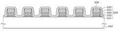
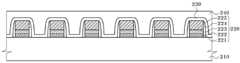
도 1 내지 도 3은 본 발명의 실시예에 따른 표면 세정을 포함하는 반도체소자 제조방법을 설명하기 위해서 개략적으로 도시한 도면들이다. 본 발명의 실시예에서는 절연층에 의한 노출되는 세정 대상층 표면을 세정하는 과정을 예시한다.1 to 3 are schematic views illustrating a method of manufacturing a semiconductor device including surface cleaning according to an embodiment of the present invention. In an embodiment of the present invention, a process of cleaning the surface of the cleaning target layer exposed by the insulating layer is illustrated.
도 1을 참조하면, 반도체 기판(110)과 같은 세정 대상층을 도입한다. 이때, 반도체 기판(110)에는 실리콘 산화물층을 포함하는 소자분리층(120)이 얕은트렌치소자분리(STI) 구조가 형성될 수 있다. 이러한 반도체 기판(110) 상에 기판 표면을 일부 노출하는 콘택홀(contact hole: 135) 또는 오프닝부(opening)를 가지는 절연층(130)이 바람직하게 실리콘산화물층을 포함하여 형성될 수 있다. 절연층(130)의 콘택홀(135)에 노출된 반도체 기판(110) 표면에는 실리콘의 자연산화에 의한 자연 산화물 등을 포함하는 표면 오염물(140)이 발생될 수 있다. 이때, 표면 오염물(140)은 콘택홀(135)의 식각에 수반된 식각잔류물을 더 포함할 수 있다.Referring to FIG. 1, a cleaning target layer such as the
도 2를 참조하면, 이러한 표면 오염물(140)을 알코올류 유기화합물에 분산된 불소(F)를 포함하는 화학종을 포함하는 식각액을 이용하여 습식 세정한다. 식각액은, 알코올류 유기화합물로 이소프로필알코올(IPA) 또는 글리콜을 적어도 80% 이상 포함할 수 있다. 또한, 이소프로필알코올 또는 글리콜에 불산(HF), 불소 이온(F-) 또는 불산 이온(HF2-)이 불소(F)를 포함하는 화학종으로 많아야 20% 미만으로 분산되어 식각액이 구성될 수 있다. 이때, 글리콜이 절연층(130)이 식각액에 의해 식각되는 정도를 보다 효과적으로 억제하는 것으로 실험적으로 평가된다. 이때, 식각액을 구성하는 성분들의 백분율(%)는 무게 백분율(wt %)로 이해된다.Referring to FIG. 2, the
절연층(130)은 BPSG를 포함하여 형성될 수 있으며, 이때, 보론은 대략 20mol% 이하, 포스포로스는 대략 30mol% 이하로 함유될 수 있다. 이러한 BPSG는 보론 및 포스포로스의 함유에 의해 실리콘 원자와 산소 원자가 자연산화물의 표면 오염물(140)에 비해 치밀하게 결합되지 못한 구조를 가지게 된다. 자연산화물의 경우 실질적으로 실리콘 원자와 산소 원자가 공유 결합을 통한 구조로 이루어지고 있으나, BPSG는 보론이나 포스포로스에 의해 이러한 공유 결합이 군데군데 끊어진 구조로 이루어지게 된다. 따라서, BPSG는 상대적으로 덜 치밀한 실리콘 산화물 구조를 가지는 것으로 이해될 수 있다.The insulating
따라서, 종래의 경우와 같이 희석불산용액을 이용하여 표면 오염물(140)을 세정 제거할 경우, 자연산화물의 식각 제거 속도에 비해 BPSG의 식각 제거 속도가 월등하게 되고, 이에 따라, 콘택홀(135)들 사이 부분이 크게 소실되어 잔류하는 부분(131)이 매우 협소해지거나 콘택홀(135)들간에 연결되게 소실될 수 있다.Therefore, when the
이에 비해 본 발명의 실시예의 식각액의 경우 불소 화학종이 실리콘 산화물의 공유 결합을 끊어주는 역할을 하지만, 글리콜 등의 성분이 BPSG의 끊어져 있는 결합기들을 패시베이션(passivation)하여 전위친화도(electro negativity) 차이를 낮춰 조절하는 역할을 하는 것으로 이해될 수 있다. 따라서, 식각액의 글리콜 등의 성분이 자연산화물에 대한 BPSG의 식각율을 낮춰주는 역할을 하는 것으로 이해될 수 있다. 따라서, 본 발명의 식각액은 자연산화물에 대한 BPSG의 식각 선택비를 보다 낮게 유도하는 효과, 예컨대, 대략 3.0 이하의 낮은 식각선택비를 구현할 수 있다.In the case of the etching solution of the present invention, the fluorine species serves to break the covalent bonds of silicon oxide, but the components such as glycol passivate the broken bond groups of the BPSG to change the difference of electro negativity. It can be understood as playing a role of lowering. Therefore, it can be understood that components such as glycol of the etching solution lower the etch rate of BPSG for the natural oxide. Accordingly, the etchant of the present invention can realize an effect of lowering the etching selectivity of the BPSG to the natural oxide, for example, a low etching selectivity of about 3.0 or less.
희석불산(DHF)을 이용한 습식 세정이나 LAL15(300: 1 BOE)의 경우 자연산화물 대비 BPSG의 식각 선택비는 적어도 5 이상으로 알려져 있으며, 일반적으로 7 내지 8 정도, 심할 경우 9 이상으로 측정되고 있다. 즉, 자연산화물에 비해 BPSG가 적어도 7-8배 정도 빠르게 식각 제거되는 것으로 평가된다.In the case of wet cleaning using dilute hydrofluoric acid (DHF) or LAL15 (300: 1 BOE), the etching selectivity ratio of BPSG to natural oxide is known to be at least 5 or more, and is generally measured to be 7 to 8 or 9 or more in severe cases. . That is, it is estimated that BPSG is etched away at least 7-8 times faster than natural oxide.
이에 비해, 본 발명의 실시예에 따른 글리콜류 및 불소 화학종을 포함하는 식각액을 이용할 경우, 바람직하게 식각 선택비가 1 이하로 구현될 수 있는 것으로 실험적으로 평가되고 있다. 즉, 자연산화물에 대비하여 BPSG와 같은 증착 산화물의 식각 속도가 실질적으로 대등하게 유도하거나 또는 BPSG 대비 자연산화물의 식각 속도가 상대적으로 높은 결과를 얻을 수 있다.On the other hand, when using an etchant comprising glycols and fluorine species according to an embodiment of the present invention, it is preferably evaluated experimentally that the etching selectivity can be implemented to 1 or less. That is, the etching rate of the deposition oxide such as BPSG may be substantially equivalent to that of the natural oxide, or the etching rate of the natural oxide may be relatively higher than that of the BPSG.
이에 따라, 자연산화물의 제거에 따른 BPSG를 포함하는 절연층(130)의 손실 또는 침식을 상대적으로 더 효과적으로 억제할 수 있다. 따라서, 절연층(130) 손실에 따른 문제들이 해소될 수 있다.Accordingly, the loss or erosion of the insulating
도 3을 참조하면, 자연산화물을 포함하는 표면 오염물(140)이 제거된 콘택홀(135)을 채우는 도전층을 형성하고, 화학기계적연마(CMP) 또는 에치백(etch-back) 등으로 평탄화하여 연결콘택(150) 또는 플러그(plug)를 형성한다. 이때, 절연층(130)의 손실이 방지되었으므로, 연결콘택(150)들 간의 격리 또한 충분히 유지될 수 있다.Referring to FIG. 3, the conductive layer filling the
이제까지 세정 대상층을 반도체 기판(110)의 단결정 실리콘층 부분(또는 이 부분에 형성된 정션층 부분)을 예시하여 설명하였지만, 본 발명의 실시예에 따른 세정은 다른 도전층 또는 실리콘층, 반도체층 표면을 세정하는 데 적용될 수 있다. 예컨대, 세정 대상층이 실리콘 기판, 다결정실리콘층, 비정질실리콘층, 텅스텐(W)층, 텅스텐질화물(WN)층, 텅스텐실리사이드(WSix)층, 티타늄(Ti)층, 티타늄질화물(TiN)층, 구리(Cu)층, 알루미늄(Al)층 또는 아연(Zn)층일 수 있다. 또한, 본 발명의 식각액은 이러한 세정 대상층이 자연산화물에 대해 낮은 선택비, 예컨대, 대략 3.0 이하의 식각선택비를 가지게 할 수 있어, 이러한 세정 대상층에의 침식을 보다 억제하며 자연산화물을 제거할 수 있다.Although the cleaning target layer has been described above by exemplifying a single crystal silicon layer portion (or a junction layer portion formed on the portion) of the
또한, 절연층(130) 또한 BPSG를 예시하였으나, 보로포스포실리케이트글래스(BPSG), 포스포실리케이트글래스(PSG), 보로실리케이트글래스(BSG), 저압-테오 스(LP-TEOS), 플라즈마개선-테오스(PE-TEOS), 고밀도플라즈마실리콘산화물(HDP silicon oxide), 언도프트실리케이트글래스(USG), 저압-질화물(LP-nitride), 플라즈마개선질화물(PE-nitride), 실리콘산질화물(SiON), 스핀온유전물(SOD) 또는 열산화물(thermal oxide)이 자연산화물에 대해서 대략 3.0 이하의 낮은 식각선택비, 바람직하게 1 이하의 식각선택비를 구현하도록 본 발명의 실시예에 의한 식각액은 유도할 수 있다.In addition, although the insulating
이와 같은 본 발명의 실시예에 따른 식각액은 자연산화물 등을 포함하는 표면 오염물(140)을 제거하는 세정에 이용될 수 있으며, 자연산화물 및 식각잔류물을 함께 제거하는 세정에도 적용될 수 있다. 또한, 본 발명의 실시예에 따른 식각액은 예시한 바와 같이 콘택(150) 형성 전 세정에 이용될 수 있으며, 또한, SAC 과정 등에도 적용될 수 있고, 다른 자연산화물의 제거를 요구하는 반도체소자 제조과정에 응용될 수 있다.Such an etching solution according to an embodiment of the present invention may be used for cleaning to remove the
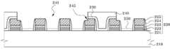
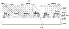
도 4 내지 도 9는 본 발명의 실시예에 따른 표면 세정을 포함하는 반도체소자 제조방법의 변형예를 설명하기 위해서 개략적으로 도시한 도면들이다.4 to 9 are schematic views illustrating a modification of the method of manufacturing a semiconductor device including surface cleaning according to an embodiment of the present invention.
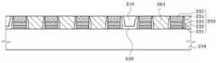
도 4를 참조하면, 본 발명의 실시예에 따른 표면 세정액 및 세정 방법은 SAC 과정에 응용될 수 있다. 이때, 층간 절연층의 소실 또는 손상에 따른 초단채널 MOS 트랜지스터의 성능 열화를 방지할 수 있어, 배선 신뢰성을 향상시킬 수 있다.4, the surface cleaning liquid and the cleaning method according to an embodiment of the present invention can be applied to the SAC process. At this time, performance degradation of the ultra-short channel MOS transistor due to the loss or damage of the interlayer insulating layer can be prevented, so that the wiring reliability can be improved.
먼저, 반도체 기판(210)에 STI 과정을 수행하고, 반도체 기판(210) 상에 게이트 스택(gate stack: 220)을 형성한다. 즉, 게이트 유전층(221), 게이트층인 제1도전층(222, 223), 측부의 실리콘질화물(SiN) 스페이서(224) 및 상부의 실리콘질화 물의 마스크층(mask layer) 또는 캡층(capping layer: 225)을 포함하는 게이트 스택(stack)들을 형성한다.First, an STI process is performed on the
이때, 스페이서(224)는 대략 5 내지 300Å 두께의 실리콘질화물(SiN)층을 포함하여 형성될 수 있다. 또한, 실리콘질화물층 및 실리콘산화물층의 이중층을 포함하여 형성될 수 있다. 또한, 제1도전층(222, 223)은 장벽 금속층 또는 다결정실리콘층의 하부 도전층(222)과, 텅스텐층 또는 텅스텐실리사이드층인 상부 도전층(223)의 복합층 구조로 형성될 수 있다. 이후에, 바람직하게 대략 1000Å 이하 두께의 언도프트실리케이트글래스(USG)층의 스페이서 절연층(230)을 형성한다. 이때, USG층은 상압화학기상증착(APCVD), 저압화학기상증착(LPCVD) 또는 원자층증착(ALD)등으로 증착될 수 있다.In this case, the
도 5를 참조하면, 게이트 스택(220)을 덮게 스페이서 절연층(230) 상에 층간 절연층(240)을 바람직하게 BPSG층을 포함하여 형성한다. BPSG층은 20mol% 이하의 보론 및 30mol% 이하의 포스포로스를 함유하게 증착될 수 있다. BPSG층을 증착한 후 CMP 등으로 평탄화한다.Referring to FIG. 5, an
도 6을 참조하면, 층간 절연층(240)을 스페이서(224) 및 캡층(225)을 식각 장벽으로 이용하여 식각하여 다수의 게이트 스택(220)들을 노출하게 확장된 콘택홀(241) 또는 오프닝부를 형성한다. 이러한 과정은 SAC 과정을 따르는 것으로 이해될 수 있다. 이때, 캡층(225)의 일부는 식각되어 소실된 부분(245)이 발생될 수도 있다.Referring to FIG. 6, the
도 7을 참조하면, 콘택홀(241)에 노출된 반도체 기판(200)의 표면에 수반된 오염물(250)을 알코올류 유기화합물에 분산된 불소(F)를 포함하는 화학종을 포함하는 식각액을 이용하여 세정한다. 이러한 세정은 도 2를 참조하여 설명한 바와 같이 층간 절연층(240)의 소실을 바람직하게 억제하며 오염물(250)의 자연산화물을 반도체 기판(200)의 표면으로부터 제거할 수 있다.Referring to FIG. 7, an etchant including a chemical species containing fluorine (F) dispersed in an alcoholic organic compound may be included in the
도 8을 참조하면, 세정된 콘택홀(241)을 채우는 제2도전층(260)을 형성한다. 제2도전층(260)은 바람직하게 도핑된 다결정 실리콘층을 증착하여 형성될 수 있다.Referring to FIG. 8, the second
도 9를 참조하면, 제2도전층(260)을 캡층(225)이 노출되게 CMP 등으로 평탄화한다. 이에 따라, 게이트 스택(220) 및 잔류하는 층간 절연층(240) 부분에 의해 분리된 연결콘택(261)들이 형성된다. 이러한 연결콘택(261)들은 트랜지스터의 정션 영역에 연결되는 플러그로도 이해될 수 있다.Referring to FIG. 9, the second
상술한 본 발명에 따르면, 자연산화물에 대한 층간 절연층 등의 낮은 식각선택비를 구현하는 세정을, 불소 화학종 및 글리콜 성분을 포함하는 식각액을 이용하여 구현할 수 있다. 이러한 세정은 자연 산화물 이외에 세정 시 사용되는 식각액에 노출되는 자연산화물 이외의 다른 막질층에의 손상을 억제할 수 있다. 즉, 자연산화물에 대한 다른 절연층 또는 도전층, 반도체층 등의 막질의 식각 선택비를 낮게 유도하여, 자연산화물의 오염물이 제거될 때 다른 막질층이 세정에 사용된 식각액에 의해 침식 또는 손상되는 것을 보다 효과적으로 방지할 수 있다.According to the present invention described above, the cleaning to implement a low etching selectivity, such as an interlayer insulating layer with respect to the natural oxide can be implemented using an etching solution containing a fluorine species and a glycol component. This cleaning can suppress damage to the film layer other than the natural oxide exposed to the etchant used during the cleaning in addition to the natural oxide. That is, by inducing a low etching selectivity of the film quality of the other insulating layer, conductive layer, semiconductor layer, etc. to the natural oxide, when the contaminants of the natural oxide is removed, the other film layer is eroded or damaged by the etchant used for cleaning Can be prevented more effectively.
따라서, 80㎚급 이하 최소 선폭의 초고집적 소자에서, 자연산화물 제거 세정에 층간절연층 등이 원하지 않게 소실되어 MOS 트랜지스터의 성능 열화가 발생되는 것을 방지할 있다. 또한, SAC 과정에서 콘택홀들 사이를 격리하는 층간 절연층 부분이 소실되어 연결콘택들 간에 누설 전류가 발생되거나 또는 단락되는 것을 방지할 수 있다. 이에 따라, 보다 신뢰성 있는 반도체 소자의 배선 구조의 형성을 구현할 수 있다.Therefore, in the ultra-high density device having a minimum line width of 80 nm or less, it is possible to prevent the deterioration of the performance of the MOS transistor due to undesired disappearance of the interlayer insulating layer or the like in the removal of the natural oxide. In addition, during the SAC process, the portion of the interlayer insulating layer that separates the contact holes may be lost to prevent leakage current or short circuit between the connection contacts. As a result, it is possible to implement formation of a wiring structure of a more reliable semiconductor element.
이상, 본 발명을 구체적인 실시예를 통하여 상세히 설명하였으나, 본 발명은 이에 한정되지 않고, 본 발명의 기술적 사상 내에서 당 분야의 통상의 지식을 가진 자에 의해 그 변형이나 개량이 가능함이 명백하다.As mentioned above, although this invention was demonstrated in detail through the specific Example, this invention is not limited to this, It is clear that the deformation | transformation and improvement are possible by the person of ordinary skill in the art within the technical idea of this invention.
Claims (24)
Translated fromKoreanPriority Applications (5)
| Application Number | Priority Date | Filing Date | Title |
|---|---|---|---|
| KR1020060078351AKR100818708B1 (en) | 2006-08-18 | 2006-08-18 | Method of manufacturing semiconductor device including surface cleaning |
| US11/771,498US20080044990A1 (en) | 2006-08-18 | 2007-06-29 | Method for Fabricating A Semiconductor Device Comprising Surface Cleaning |
| TW096125497ATW200811935A (en) | 2006-08-18 | 2007-07-13 | Method for fabricating a semiconductor device comprising surface cleaning |
| JP2007204914AJP2008047898A (en) | 2006-08-18 | 2007-08-07 | Method for manufacturing semiconductor element |
| CNB2007101426730ACN100561665C (en) | 2006-08-18 | 2007-08-20 | Method for manufacturing semiconductor device including surface cleaning step |
Applications Claiming Priority (1)
| Application Number | Priority Date | Filing Date | Title |
|---|---|---|---|
| KR1020060078351AKR100818708B1 (en) | 2006-08-18 | 2006-08-18 | Method of manufacturing semiconductor device including surface cleaning |
Publications (2)
| Publication Number | Publication Date |
|---|---|
| KR20080016338A KR20080016338A (en) | 2008-02-21 |
| KR100818708B1true KR100818708B1 (en) | 2008-04-01 |
Family
ID=39095284
Family Applications (1)
| Application Number | Title | Priority Date | Filing Date |
|---|---|---|---|
| KR1020060078351AExpired - Fee RelatedKR100818708B1 (en) | 2006-08-18 | 2006-08-18 | Method of manufacturing semiconductor device including surface cleaning |
Country Status (5)
| Country | Link |
|---|---|
| US (1) | US20080044990A1 (en) |
| JP (1) | JP2008047898A (en) |
| KR (1) | KR100818708B1 (en) |
| CN (1) | CN100561665C (en) |
| TW (1) | TW200811935A (en) |
Cited By (1)
| Publication number | Priority date | Publication date | Assignee | Title |
|---|---|---|---|---|
| WO2021257537A1 (en)* | 2020-06-19 | 2021-12-23 | Applied Materials, Inc. | Methods and apparatus for aluminum oxide surface recovery |
Families Citing this family (183)
| Publication number | Priority date | Publication date | Assignee | Title |
|---|---|---|---|---|
| AU2006326405B2 (en) | 2005-12-13 | 2013-10-31 | President And Fellows Of Harvard College | Scaffolds for cell transplantation |
| US9770535B2 (en) | 2007-06-21 | 2017-09-26 | President And Fellows Of Harvard College | Scaffolds for cell collection or elimination |
| KR101406888B1 (en)* | 2007-12-13 | 2014-06-30 | 삼성전자주식회사 | Method of manufacturing semiconductor device |
| CN102006891B (en) | 2008-02-13 | 2017-04-26 | 哈佛学院董事会 | Continuous cell programming device |
| US9370558B2 (en) | 2008-02-13 | 2016-06-21 | President And Fellows Of Harvard College | Controlled delivery of TLR agonists in structural polymeric devices |
| US9012399B2 (en)* | 2008-05-30 | 2015-04-21 | President And Fellows Of Harvard College | Controlled release of growth factors and signaling molecules for promoting angiogenesis |
| US8252119B2 (en)* | 2008-08-20 | 2012-08-28 | Micron Technology, Inc. | Microelectronic substrate cleaning systems with polyelectrolyte and associated methods |
| US8398779B2 (en)* | 2009-03-02 | 2013-03-19 | Applied Materials, Inc. | Non destructive selective deposition removal of non-metallic deposits from aluminum containing substrates |
| US9297005B2 (en) | 2009-04-13 | 2016-03-29 | President And Fellows Of Harvard College | Harnessing cell dynamics to engineer materials |
| EP2461828B1 (en) | 2009-07-31 | 2017-06-21 | President and Fellows of Harvard College | Programming of cells for tolerogenic therapies |
| CN102082091B (en)* | 2009-11-30 | 2012-07-11 | 上海华虹Nec电子有限公司 | Method for improving appearance of phosphosilicate glass by virtue of high-density plasma chemical vapor deposition (HDP CVD) |
| CN102087963B (en)* | 2009-12-04 | 2013-08-14 | 无锡华润上华半导体有限公司 | Method for etching polycrystalline silicon layer |
| CN102157435B (en)* | 2010-02-11 | 2013-01-30 | 中芯国际集成电路制造(上海)有限公司 | Contact hole forming method |
| WO2011109834A2 (en) | 2010-03-05 | 2011-09-09 | President And Fellows Of Harvard College | Enhancement of skeletal muscle stem cell engrafment by dual delivery of vegf and igf-1 |
| US9324576B2 (en) | 2010-05-27 | 2016-04-26 | Applied Materials, Inc. | Selective etch for silicon films |
| US9693954B2 (en) | 2010-06-25 | 2017-07-04 | President And Fellows Of Harvard College | Co-delivery of stimulatory and inhibitory factors to create temporally stable and spatially restricted zones |
| US20130052774A1 (en)* | 2010-06-29 | 2013-02-28 | Kyocera Corporation | Method for surface-treating semiconductor substrate, semiconductor substrate, and method for producing solar battery |
| EP2608249B1 (en)* | 2010-08-20 | 2019-02-27 | Mitsubishi Gas Chemical Company, Inc. | Method for producing transistor |
| PL2624873T3 (en) | 2010-10-06 | 2020-12-14 | President And Fellows Of Harvard College | Injectable, pore-forming hydrogels for materials-based cell therapies |
| WO2012064697A2 (en) | 2010-11-08 | 2012-05-18 | President And Fellows Of Harvard College | Materials presenting notch signaling molecules to control cell behavior |
| US10283321B2 (en) | 2011-01-18 | 2019-05-07 | Applied Materials, Inc. | Semiconductor processing system and methods using capacitively coupled plasma |
| US9064815B2 (en) | 2011-03-14 | 2015-06-23 | Applied Materials, Inc. | Methods for etch of metal and metal-oxide films |
| US8999856B2 (en) | 2011-03-14 | 2015-04-07 | Applied Materials, Inc. | Methods for etch of sin films |
| WO2012148684A1 (en) | 2011-04-27 | 2012-11-01 | President And Fellows Of Harvard College | Cell-friendly inverse opal hydrogels for cell encapsulation, drug and protein delivery, and functional nanoparticle encapsulation |
| US9675561B2 (en) | 2011-04-28 | 2017-06-13 | President And Fellows Of Harvard College | Injectable cryogel vaccine devices and methods of use thereof |
| EP3417876B1 (en) | 2011-04-28 | 2021-03-31 | President and Fellows of Harvard College | Injectable preformed macroscopic 3-dimensional scaffolds for minimally invasive administration |
| US9486512B2 (en) | 2011-06-03 | 2016-11-08 | President And Fellows Of Harvard College | In situ antigen-generating cancer vaccine |
| KR20130010362A (en)* | 2011-07-18 | 2013-01-28 | 삼성전자주식회사 | Method for fabricating semiconductor device |
| US8771536B2 (en) | 2011-08-01 | 2014-07-08 | Applied Materials, Inc. | Dry-etch for silicon-and-carbon-containing films |
| US8927390B2 (en) | 2011-09-26 | 2015-01-06 | Applied Materials, Inc. | Intrench profile |
| US20130260564A1 (en)* | 2011-09-26 | 2013-10-03 | Applied Materials, Inc. | Insensitive dry removal process for semiconductor integration |
| US8808563B2 (en) | 2011-10-07 | 2014-08-19 | Applied Materials, Inc. | Selective etch of silicon by way of metastable hydrogen termination |
| CN103178049B (en)* | 2011-12-22 | 2015-10-14 | 上海华虹宏力半导体制造有限公司 | The structure of self-aligned contact hole insulating barrier and preparation method |
| JP5548225B2 (en) | 2012-03-16 | 2014-07-16 | 富士フイルム株式会社 | Semiconductor substrate product manufacturing method and etching solution |
| EP2838515B1 (en) | 2012-04-16 | 2019-11-20 | President and Fellows of Harvard College | Mesoporous silica compositions for modulating immune responses |
| US9267739B2 (en) | 2012-07-18 | 2016-02-23 | Applied Materials, Inc. | Pedestal with multi-zone temperature control and multiple purge capabilities |
| US9373517B2 (en) | 2012-08-02 | 2016-06-21 | Applied Materials, Inc. | Semiconductor processing with DC assisted RF power for improved control |
| US9034770B2 (en) | 2012-09-17 | 2015-05-19 | Applied Materials, Inc. | Differential silicon oxide etch |
| US9023734B2 (en) | 2012-09-18 | 2015-05-05 | Applied Materials, Inc. | Radical-component oxide etch |
| US9390937B2 (en) | 2012-09-20 | 2016-07-12 | Applied Materials, Inc. | Silicon-carbon-nitride selective etch |
| US9132436B2 (en) | 2012-09-21 | 2015-09-15 | Applied Materials, Inc. | Chemical control features in wafer process equipment |
| US8969212B2 (en) | 2012-11-20 | 2015-03-03 | Applied Materials, Inc. | Dry-etch selectivity |
| US9064816B2 (en) | 2012-11-30 | 2015-06-23 | Applied Materials, Inc. | Dry-etch for selective oxidation removal |
| US8980763B2 (en) | 2012-11-30 | 2015-03-17 | Applied Materials, Inc. | Dry-etch for selective tungsten removal |
| US9111877B2 (en) | 2012-12-18 | 2015-08-18 | Applied Materials, Inc. | Non-local plasma oxide etch |
| US8921234B2 (en) | 2012-12-21 | 2014-12-30 | Applied Materials, Inc. | Selective titanium nitride etching |
| US10256079B2 (en) | 2013-02-08 | 2019-04-09 | Applied Materials, Inc. | Semiconductor processing systems having multiple plasma configurations |
| US9362130B2 (en) | 2013-03-01 | 2016-06-07 | Applied Materials, Inc. | Enhanced etching processes using remote plasma sources |
| US9040422B2 (en) | 2013-03-05 | 2015-05-26 | Applied Materials, Inc. | Selective titanium nitride removal |
| US8801952B1 (en) | 2013-03-07 | 2014-08-12 | Applied Materials, Inc. | Conformal oxide dry etch |
| US10170282B2 (en) | 2013-03-08 | 2019-01-01 | Applied Materials, Inc. | Insulated semiconductor faceplate designs |
| US20140271097A1 (en) | 2013-03-15 | 2014-09-18 | Applied Materials, Inc. | Processing systems and methods for halide scavenging |
| KR101790090B1 (en)* | 2013-05-02 | 2017-10-25 | 후지필름 가부시키가이샤 | Etching method, etching liquid and etching liquid kit to be used in said method, and semiconductor substrate product manufacturing method |
| US8895449B1 (en) | 2013-05-16 | 2014-11-25 | Applied Materials, Inc. | Delicate dry clean |
| US9114438B2 (en) | 2013-05-21 | 2015-08-25 | Applied Materials, Inc. | Copper residue chamber clean |
| US9493879B2 (en) | 2013-07-12 | 2016-11-15 | Applied Materials, Inc. | Selective sputtering for pattern transfer |
| US9773648B2 (en) | 2013-08-30 | 2017-09-26 | Applied Materials, Inc. | Dual discharge modes operation for remote plasma |
| US8956980B1 (en) | 2013-09-16 | 2015-02-17 | Applied Materials, Inc. | Selective etch of silicon nitride |
| US8951429B1 (en) | 2013-10-29 | 2015-02-10 | Applied Materials, Inc. | Tungsten oxide processing |
| US9236265B2 (en) | 2013-11-04 | 2016-01-12 | Applied Materials, Inc. | Silicon germanium processing |
| US9576809B2 (en) | 2013-11-04 | 2017-02-21 | Applied Materials, Inc. | Etch suppression with germanium |
| US9520303B2 (en) | 2013-11-12 | 2016-12-13 | Applied Materials, Inc. | Aluminum selective etch |
| US9245762B2 (en) | 2013-12-02 | 2016-01-26 | Applied Materials, Inc. | Procedure for etch rate consistency |
| US9117855B2 (en) | 2013-12-04 | 2015-08-25 | Applied Materials, Inc. | Polarity control for remote plasma |
| US9287095B2 (en) | 2013-12-17 | 2016-03-15 | Applied Materials, Inc. | Semiconductor system assemblies and methods of operation |
| US9263278B2 (en) | 2013-12-17 | 2016-02-16 | Applied Materials, Inc. | Dopant etch selectivity control |
| US9190293B2 (en) | 2013-12-18 | 2015-11-17 | Applied Materials, Inc. | Even tungsten etch for high aspect ratio trenches |
| US9287134B2 (en) | 2014-01-17 | 2016-03-15 | Applied Materials, Inc. | Titanium oxide etch |
| US9293568B2 (en) | 2014-01-27 | 2016-03-22 | Applied Materials, Inc. | Method of fin patterning |
| US9396989B2 (en) | 2014-01-27 | 2016-07-19 | Applied Materials, Inc. | Air gaps between copper lines |
| US9385028B2 (en) | 2014-02-03 | 2016-07-05 | Applied Materials, Inc. | Air gap process |
| US9499898B2 (en) | 2014-03-03 | 2016-11-22 | Applied Materials, Inc. | Layered thin film heater and method of fabrication |
| US9299575B2 (en) | 2014-03-17 | 2016-03-29 | Applied Materials, Inc. | Gas-phase tungsten etch |
| US9299538B2 (en) | 2014-03-20 | 2016-03-29 | Applied Materials, Inc. | Radial waveguide systems and methods for post-match control of microwaves |
| US9299537B2 (en) | 2014-03-20 | 2016-03-29 | Applied Materials, Inc. | Radial waveguide systems and methods for post-match control of microwaves |
| US9136273B1 (en) | 2014-03-21 | 2015-09-15 | Applied Materials, Inc. | Flash gate air gap |
| US9903020B2 (en) | 2014-03-31 | 2018-02-27 | Applied Materials, Inc. | Generation of compact alumina passivation layers on aluminum plasma equipment components |
| US9269590B2 (en) | 2014-04-07 | 2016-02-23 | Applied Materials, Inc. | Spacer formation |
| WO2015168379A2 (en) | 2014-04-30 | 2015-11-05 | President And Fellows Of Harvard College | Combination vaccine devices and methods of killing cancer cells |
| US9309598B2 (en) | 2014-05-28 | 2016-04-12 | Applied Materials, Inc. | Oxide and metal removal |
| US9847289B2 (en) | 2014-05-30 | 2017-12-19 | Applied Materials, Inc. | Protective via cap for improved interconnect performance |
| US9406523B2 (en) | 2014-06-19 | 2016-08-02 | Applied Materials, Inc. | Highly selective doped oxide removal method |
| US9378969B2 (en) | 2014-06-19 | 2016-06-28 | Applied Materials, Inc. | Low temperature gas-phase carbon removal |
| US20150371925A1 (en)* | 2014-06-20 | 2015-12-24 | Intel Corporation | Through array routing for non-volatile memory |
| US9425058B2 (en) | 2014-07-24 | 2016-08-23 | Applied Materials, Inc. | Simplified litho-etch-litho-etch process |
| US9159606B1 (en) | 2014-07-31 | 2015-10-13 | Applied Materials, Inc. | Metal air gap |
| US9496167B2 (en) | 2014-07-31 | 2016-11-15 | Applied Materials, Inc. | Integrated bit-line airgap formation and gate stack post clean |
| US9378978B2 (en) | 2014-07-31 | 2016-06-28 | Applied Materials, Inc. | Integrated oxide recess and floating gate fin trimming |
| US9165786B1 (en) | 2014-08-05 | 2015-10-20 | Applied Materials, Inc. | Integrated oxide and nitride recess for better channel contact in 3D architectures |
| US9659753B2 (en) | 2014-08-07 | 2017-05-23 | Applied Materials, Inc. | Grooved insulator to reduce leakage current |
| US9553102B2 (en) | 2014-08-19 | 2017-01-24 | Applied Materials, Inc. | Tungsten separation |
| US9355856B2 (en) | 2014-09-12 | 2016-05-31 | Applied Materials, Inc. | V trench dry etch |
| US9355862B2 (en) | 2014-09-24 | 2016-05-31 | Applied Materials, Inc. | Fluorine-based hardmask removal |
| US9368364B2 (en) | 2014-09-24 | 2016-06-14 | Applied Materials, Inc. | Silicon etch process with tunable selectivity to SiO2 and other materials |
| US9613822B2 (en) | 2014-09-25 | 2017-04-04 | Applied Materials, Inc. | Oxide etch selectivity enhancement |
| US9966240B2 (en) | 2014-10-14 | 2018-05-08 | Applied Materials, Inc. | Systems and methods for internal surface conditioning assessment in plasma processing equipment |
| US9355922B2 (en) | 2014-10-14 | 2016-05-31 | Applied Materials, Inc. | Systems and methods for internal surface conditioning in plasma processing equipment |
| US11637002B2 (en) | 2014-11-26 | 2023-04-25 | Applied Materials, Inc. | Methods and systems to enhance process uniformity |
| US9299583B1 (en) | 2014-12-05 | 2016-03-29 | Applied Materials, Inc. | Aluminum oxide selective etch |
| US10573496B2 (en) | 2014-12-09 | 2020-02-25 | Applied Materials, Inc. | Direct outlet toroidal plasma source |
| US10224210B2 (en) | 2014-12-09 | 2019-03-05 | Applied Materials, Inc. | Plasma processing system with direct outlet toroidal plasma source |
| US9502258B2 (en) | 2014-12-23 | 2016-11-22 | Applied Materials, Inc. | Anisotropic gap etch |
| US9343272B1 (en) | 2015-01-08 | 2016-05-17 | Applied Materials, Inc. | Self-aligned process |
| US11257693B2 (en) | 2015-01-09 | 2022-02-22 | Applied Materials, Inc. | Methods and systems to improve pedestal temperature control |
| US9373522B1 (en) | 2015-01-22 | 2016-06-21 | Applied Mateials, Inc. | Titanium nitride removal |
| US9449846B2 (en) | 2015-01-28 | 2016-09-20 | Applied Materials, Inc. | Vertical gate separation |
| CA3012602A1 (en) | 2015-01-30 | 2016-08-04 | President And Fellows Of Harvard College | Peritumoral and intratumoral materials for cancer therapy |
| US9728437B2 (en) | 2015-02-03 | 2017-08-08 | Applied Materials, Inc. | High temperature chuck for plasma processing systems |
| US20160225652A1 (en) | 2015-02-03 | 2016-08-04 | Applied Materials, Inc. | Low temperature chuck for plasma processing systems |
| US9881805B2 (en) | 2015-03-02 | 2018-01-30 | Applied Materials, Inc. | Silicon selective removal |
| WO2016164705A1 (en) | 2015-04-10 | 2016-10-13 | Omar Abdel-Rahman Ali | Immune cell trapping devices and methods for making and using the same |
| US9741593B2 (en) | 2015-08-06 | 2017-08-22 | Applied Materials, Inc. | Thermal management systems and methods for wafer processing systems |
| US9691645B2 (en) | 2015-08-06 | 2017-06-27 | Applied Materials, Inc. | Bolted wafer chuck thermal management systems and methods for wafer processing systems |
| US9349605B1 (en) | 2015-08-07 | 2016-05-24 | Applied Materials, Inc. | Oxide etch selectivity systems and methods |
| US10504700B2 (en) | 2015-08-27 | 2019-12-10 | Applied Materials, Inc. | Plasma etching systems and methods with secondary plasma injection |
| US9460959B1 (en)* | 2015-10-02 | 2016-10-04 | Applied Materials, Inc. | Methods for pre-cleaning conductive interconnect structures |
| CN115531609A (en) | 2016-02-06 | 2022-12-30 | 哈佛学院校长同事会 | Remodeling hematopoietic niches to reconstitute immunity |
| US10522371B2 (en) | 2016-05-19 | 2019-12-31 | Applied Materials, Inc. | Systems and methods for improved semiconductor etching and component protection |
| US10504754B2 (en) | 2016-05-19 | 2019-12-10 | Applied Materials, Inc. | Systems and methods for improved semiconductor etching and component protection |
| US9865484B1 (en) | 2016-06-29 | 2018-01-09 | Applied Materials, Inc. | Selective etch using material modification and RF pulsing |
| CN115404196A (en) | 2016-07-13 | 2022-11-29 | 哈佛学院院长等 | Antigen-presenting cell mimic scaffold and methods for its preparation and use |
| JP7274214B2 (en) | 2016-08-02 | 2023-05-16 | プレジデント アンド フェローズ オブ ハーバード カレッジ | Biomaterials for modulating immune responses |
| US10062575B2 (en) | 2016-09-09 | 2018-08-28 | Applied Materials, Inc. | Poly directional etch by oxidation |
| US10629473B2 (en) | 2016-09-09 | 2020-04-21 | Applied Materials, Inc. | Footing removal for nitride spacer |
| US9721789B1 (en) | 2016-10-04 | 2017-08-01 | Applied Materials, Inc. | Saving ion-damaged spacers |
| US9934942B1 (en) | 2016-10-04 | 2018-04-03 | Applied Materials, Inc. | Chamber with flow-through source |
| US10546729B2 (en) | 2016-10-04 | 2020-01-28 | Applied Materials, Inc. | Dual-channel showerhead with improved profile |
| US10062585B2 (en) | 2016-10-04 | 2018-08-28 | Applied Materials, Inc. | Oxygen compatible plasma source |
| US10062579B2 (en) | 2016-10-07 | 2018-08-28 | Applied Materials, Inc. | Selective SiN lateral recess |
| US9947549B1 (en) | 2016-10-10 | 2018-04-17 | Applied Materials, Inc. | Cobalt-containing material removal |
| US9768034B1 (en) | 2016-11-11 | 2017-09-19 | Applied Materials, Inc. | Removal methods for high aspect ratio structures |
| US10163696B2 (en) | 2016-11-11 | 2018-12-25 | Applied Materials, Inc. | Selective cobalt removal for bottom up gapfill |
| US10026621B2 (en) | 2016-11-14 | 2018-07-17 | Applied Materials, Inc. | SiN spacer profile patterning |
| US10242908B2 (en) | 2016-11-14 | 2019-03-26 | Applied Materials, Inc. | Airgap formation with damage-free copper |
| US10566206B2 (en) | 2016-12-27 | 2020-02-18 | Applied Materials, Inc. | Systems and methods for anisotropic material breakthrough |
| US10403507B2 (en) | 2017-02-03 | 2019-09-03 | Applied Materials, Inc. | Shaped etch profile with oxidation |
| US10431429B2 (en) | 2017-02-03 | 2019-10-01 | Applied Materials, Inc. | Systems and methods for radial and azimuthal control of plasma uniformity |
| US10043684B1 (en) | 2017-02-06 | 2018-08-07 | Applied Materials, Inc. | Self-limiting atomic thermal etching systems and methods |
| US10319739B2 (en) | 2017-02-08 | 2019-06-11 | Applied Materials, Inc. | Accommodating imperfectly aligned memory holes |
| US10943834B2 (en) | 2017-03-13 | 2021-03-09 | Applied Materials, Inc. | Replacement contact process |
| US10319649B2 (en) | 2017-04-11 | 2019-06-11 | Applied Materials, Inc. | Optical emission spectroscopy (OES) for remote plasma monitoring |
| US11276590B2 (en) | 2017-05-17 | 2022-03-15 | Applied Materials, Inc. | Multi-zone semiconductor substrate supports |
| US11276559B2 (en) | 2017-05-17 | 2022-03-15 | Applied Materials, Inc. | Semiconductor processing chamber for multiple precursor flow |
| JP7176860B6 (en) | 2017-05-17 | 2022-12-16 | アプライド マテリアルズ インコーポレイテッド | Semiconductor processing chamber to improve precursor flow |
| US10049891B1 (en) | 2017-05-31 | 2018-08-14 | Applied Materials, Inc. | Selective in situ cobalt residue removal |
| US10497579B2 (en) | 2017-05-31 | 2019-12-03 | Applied Materials, Inc. | Water-free etching methods |
| US10920320B2 (en) | 2017-06-16 | 2021-02-16 | Applied Materials, Inc. | Plasma health determination in semiconductor substrate processing reactors |
| US10541246B2 (en) | 2017-06-26 | 2020-01-21 | Applied Materials, Inc. | 3D flash memory cells which discourage cross-cell electrical tunneling |
| US10727080B2 (en) | 2017-07-07 | 2020-07-28 | Applied Materials, Inc. | Tantalum-containing material removal |
| US10541184B2 (en) | 2017-07-11 | 2020-01-21 | Applied Materials, Inc. | Optical emission spectroscopic techniques for monitoring etching |
| US10354889B2 (en) | 2017-07-17 | 2019-07-16 | Applied Materials, Inc. | Non-halogen etching of silicon-containing materials |
| US10043674B1 (en) | 2017-08-04 | 2018-08-07 | Applied Materials, Inc. | Germanium etching systems and methods |
| US10170336B1 (en) | 2017-08-04 | 2019-01-01 | Applied Materials, Inc. | Methods for anisotropic control of selective silicon removal |
| US10297458B2 (en) | 2017-08-07 | 2019-05-21 | Applied Materials, Inc. | Process window widening using coated parts in plasma etch processes |
| US10283324B1 (en) | 2017-10-24 | 2019-05-07 | Applied Materials, Inc. | Oxygen treatment for nitride etching |
| US10128086B1 (en) | 2017-10-24 | 2018-11-13 | Applied Materials, Inc. | Silicon pretreatment for nitride removal |
| US10256112B1 (en) | 2017-12-08 | 2019-04-09 | Applied Materials, Inc. | Selective tungsten removal |
| US10903054B2 (en) | 2017-12-19 | 2021-01-26 | Applied Materials, Inc. | Multi-zone gas distribution systems and methods |
| US11328909B2 (en) | 2017-12-22 | 2022-05-10 | Applied Materials, Inc. | Chamber conditioning and removal processes |
| US10854426B2 (en) | 2018-01-08 | 2020-12-01 | Applied Materials, Inc. | Metal recess for semiconductor structures |
| US10679870B2 (en) | 2018-02-15 | 2020-06-09 | Applied Materials, Inc. | Semiconductor processing chamber multistage mixing apparatus |
| US10964512B2 (en) | 2018-02-15 | 2021-03-30 | Applied Materials, Inc. | Semiconductor processing chamber multistage mixing apparatus and methods |
| TWI766433B (en) | 2018-02-28 | 2022-06-01 | 美商應用材料股份有限公司 | Systems and methods to form airgaps |
| US10593560B2 (en) | 2018-03-01 | 2020-03-17 | Applied Materials, Inc. | Magnetic induction plasma source for semiconductor processes and equipment |
| US10319600B1 (en) | 2018-03-12 | 2019-06-11 | Applied Materials, Inc. | Thermal silicon etch |
| US10497573B2 (en) | 2018-03-13 | 2019-12-03 | Applied Materials, Inc. | Selective atomic layer etching of semiconductor materials |
| US10573527B2 (en) | 2018-04-06 | 2020-02-25 | Applied Materials, Inc. | Gas-phase selective etching systems and methods |
| US10490406B2 (en) | 2018-04-10 | 2019-11-26 | Appled Materials, Inc. | Systems and methods for material breakthrough |
| US10699879B2 (en) | 2018-04-17 | 2020-06-30 | Applied Materials, Inc. | Two piece electrode assembly with gap for plasma control |
| US10886137B2 (en) | 2018-04-30 | 2021-01-05 | Applied Materials, Inc. | Selective nitride removal |
| US10872778B2 (en) | 2018-07-06 | 2020-12-22 | Applied Materials, Inc. | Systems and methods utilizing solid-phase etchants |
| US10755941B2 (en) | 2018-07-06 | 2020-08-25 | Applied Materials, Inc. | Self-limiting selective etching systems and methods |
| US10672642B2 (en) | 2018-07-24 | 2020-06-02 | Applied Materials, Inc. | Systems and methods for pedestal configuration |
| US11049755B2 (en) | 2018-09-14 | 2021-06-29 | Applied Materials, Inc. | Semiconductor substrate supports with embedded RF shield |
| US10892198B2 (en) | 2018-09-14 | 2021-01-12 | Applied Materials, Inc. | Systems and methods for improved performance in semiconductor processing |
| US11062887B2 (en) | 2018-09-17 | 2021-07-13 | Applied Materials, Inc. | High temperature RF heater pedestals |
| WO2020061129A1 (en) | 2018-09-19 | 2020-03-26 | President And Fellows Of Harvard College | Compositions and methods for labeling and modulation of cells in vitro and in vivo |
| US11417534B2 (en) | 2018-09-21 | 2022-08-16 | Applied Materials, Inc. | Selective material removal |
| US11682560B2 (en) | 2018-10-11 | 2023-06-20 | Applied Materials, Inc. | Systems and methods for hafnium-containing film removal |
| US11121002B2 (en) | 2018-10-24 | 2021-09-14 | Applied Materials, Inc. | Systems and methods for etching metals and metal derivatives |
| US11437242B2 (en) | 2018-11-27 | 2022-09-06 | Applied Materials, Inc. | Selective removal of silicon-containing materials |
| US11721527B2 (en) | 2019-01-07 | 2023-08-08 | Applied Materials, Inc. | Processing chamber mixing systems |
| US10920319B2 (en) | 2019-01-11 | 2021-02-16 | Applied Materials, Inc. | Ceramic showerheads with conductive electrodes |
Citations (5)
| Publication number | Priority date | Publication date | Assignee | Title |
|---|---|---|---|---|
| JP2001305752A (en) | 2000-04-26 | 2001-11-02 | Daikin Ind Ltd | Polymer stripper composition for fine patterns |
| KR20030035207A (en)* | 2001-10-30 | 2003-05-09 | 에이펫(주) | cleaning solution for semiconductor device and for semiconductor device-cleaning method using the same |
| KR20050109569A (en)* | 2003-03-17 | 2005-11-21 | 다이킨 고교 가부시키가이샤 | Process for production of etching or cleaning fluids |
| KR20060005845A (en)* | 2004-07-14 | 2006-01-18 | 테크노세미켐 주식회사 | Semiconductor substrate cleaning composition, semiconductor substrate cleaning method and semiconductor device manufacturing method using same |
| KR20060086839A (en)* | 2002-10-31 | 2006-08-01 | 어드밴스드 테크놀러지 머티리얼즈, 인코포레이티드 | Supercritical Carbon Dioxide / Chemical Composition for Removing Residues After Ashing and Un-Asing Aluminum Etching |
Family Cites Families (9)
| Publication number | Priority date | Publication date | Assignee | Title |
|---|---|---|---|---|
| JPH1050647A (en)* | 1996-05-14 | 1998-02-20 | Samsung Electron Co Ltd | Cleaning solution and cleaning method using the same |
| US6240933B1 (en)* | 1997-05-09 | 2001-06-05 | Semitool, Inc. | Methods for cleaning semiconductor surfaces |
| JPH11323394A (en)* | 1998-05-14 | 1999-11-26 | Texas Instr Japan Ltd | Cleaning agent for semiconductor device manufacturing and method for manufacturing semiconductor device using the same |
| DE19844102C2 (en)* | 1998-09-25 | 2000-07-20 | Siemens Ag | Manufacturing process for a semiconductor structure |
| KR100307287B1 (en)* | 1998-11-20 | 2001-12-05 | 윤종용 | Manufacturing method of pad of semiconductor device |
| TW518719B (en)* | 2001-10-26 | 2003-01-21 | Promos Technologies Inc | Manufacturing method of contact plug |
| US7045073B2 (en)* | 2002-12-18 | 2006-05-16 | Intel Corporation | Pre-etch implantation damage for the removal of thin film layers |
| KR100645458B1 (en)* | 2003-10-02 | 2006-11-13 | 주식회사 하이닉스반도체 | Manufacturing method of semiconductor device which can prevent attack by wet cleaning |
| US7253094B1 (en)* | 2003-12-22 | 2007-08-07 | Cypress Semiconductor Corp. | Methods for cleaning contact openings to reduce contact resistance |
- 2006
- 2006-08-18KRKR1020060078351Apatent/KR100818708B1/ennot_activeExpired - Fee Related
- 2007
- 2007-06-29USUS11/771,498patent/US20080044990A1/ennot_activeAbandoned
- 2007-07-13TWTW096125497Apatent/TW200811935A/enunknown
- 2007-08-07JPJP2007204914Apatent/JP2008047898A/enactivePending
- 2007-08-20CNCNB2007101426730Apatent/CN100561665C/ennot_activeExpired - Fee Related
Patent Citations (5)
| Publication number | Priority date | Publication date | Assignee | Title |
|---|---|---|---|---|
| JP2001305752A (en) | 2000-04-26 | 2001-11-02 | Daikin Ind Ltd | Polymer stripper composition for fine patterns |
| KR20030035207A (en)* | 2001-10-30 | 2003-05-09 | 에이펫(주) | cleaning solution for semiconductor device and for semiconductor device-cleaning method using the same |
| KR20060086839A (en)* | 2002-10-31 | 2006-08-01 | 어드밴스드 테크놀러지 머티리얼즈, 인코포레이티드 | Supercritical Carbon Dioxide / Chemical Composition for Removing Residues After Ashing and Un-Asing Aluminum Etching |
| KR20050109569A (en)* | 2003-03-17 | 2005-11-21 | 다이킨 고교 가부시키가이샤 | Process for production of etching or cleaning fluids |
| KR20060005845A (en)* | 2004-07-14 | 2006-01-18 | 테크노세미켐 주식회사 | Semiconductor substrate cleaning composition, semiconductor substrate cleaning method and semiconductor device manufacturing method using same |
Cited By (1)
| Publication number | Priority date | Publication date | Assignee | Title |
|---|---|---|---|---|
| WO2021257537A1 (en)* | 2020-06-19 | 2021-12-23 | Applied Materials, Inc. | Methods and apparatus for aluminum oxide surface recovery |
Also Published As
| Publication number | Publication date |
|---|---|
| US20080044990A1 (en) | 2008-02-21 |
| JP2008047898A (en) | 2008-02-28 |
| CN101127299A (en) | 2008-02-20 |
| KR20080016338A (en) | 2008-02-21 |
| CN100561665C (en) | 2009-11-18 |
| TW200811935A (en) | 2008-03-01 |
Similar Documents
| Publication | Publication Date | Title |
|---|---|---|
| KR100818708B1 (en) | Method of manufacturing semiconductor device including surface cleaning | |
| US7875547B2 (en) | Contact hole structures and contact structures and fabrication methods thereof | |
| KR20030056149A (en) | Method for fabricating semiconductor device | |
| TW201743406A (en) | Method of fabricating semiconductor structure | |
| US8598012B2 (en) | Method for fabricating semiconductor device with buried gates | |
| US7981762B2 (en) | Method of forming pre-metal dielectric layer of semiconductor device | |
| US7879736B2 (en) | Composition for etching silicon oxide and method of forming a contact hole using the same | |
| KR20090001377A (en) | Method of forming a semiconductor device | |
| US7649218B2 (en) | Lateral MOS transistor and method for manufacturing thereof | |
| US7825030B2 (en) | Method of forming a spacer | |
| KR20070093794A (en) | Method for manufacturing contact plug of semiconductor device | |
| US7508029B2 (en) | Semiconductor device and method for fabricating the same | |
| KR100791707B1 (en) | Method of planarizing interlayer insulating film of semiconductor device | |
| KR20100004648A (en) | Method for manufacturing capacitor in semiconductor device | |
| KR100744001B1 (en) | How to Form Landing Plug Contacts | |
| KR20090061354A (en) | Cleaning solution for removing impurities, substrate cleaning method and manufacturing method of semiconductor device using same | |
| KR100482754B1 (en) | Method for manufacturing a capacitor in semiconductor device | |
| KR100637100B1 (en) | Metal plug formation method of semiconductor device | |
| KR100861372B1 (en) | Method of forming polyside gate of semiconductor device | |
| KR20060067393A (en) | How to form a dual damascene pattern | |
| KR100952243B1 (en) | Method for manufacturing intermetallic insulating layer of semiconductor device | |
| KR100537185B1 (en) | Method for fabrication of semiconductor device | |
| CN117238759A (en) | Method for improving metal aluminum gate loss | |
| KR20100079015A (en) | Method for forming contact for metal line | |
| KR20040001949A (en) | Method for fabricating semiconductor device |
Legal Events
| Date | Code | Title | Description |
|---|---|---|---|
| A201 | Request for examination | ||
| PA0109 | Patent application | St.27 status event code:A-0-1-A10-A12-nap-PA0109 | |
| PA0201 | Request for examination | St.27 status event code:A-1-2-D10-D11-exm-PA0201 | |
| D13-X000 | Search requested | St.27 status event code:A-1-2-D10-D13-srh-X000 | |
| D14-X000 | Search report completed | St.27 status event code:A-1-2-D10-D14-srh-X000 | |
| E902 | Notification of reason for refusal | ||
| PE0902 | Notice of grounds for rejection | St.27 status event code:A-1-2-D10-D21-exm-PE0902 | |
| E13-X000 | Pre-grant limitation requested | St.27 status event code:A-2-3-E10-E13-lim-X000 | |
| P11-X000 | Amendment of application requested | St.27 status event code:A-2-2-P10-P11-nap-X000 | |
| P13-X000 | Application amended | St.27 status event code:A-2-2-P10-P13-nap-X000 | |
| E701 | Decision to grant or registration of patent right | ||
| PE0701 | Decision of registration | St.27 status event code:A-1-2-D10-D22-exm-PE0701 | |
| PG1501 | Laying open of application | St.27 status event code:A-1-1-Q10-Q12-nap-PG1501 | |
| GRNT | Written decision to grant | ||
| PR0701 | Registration of establishment | St.27 status event code:A-2-4-F10-F11-exm-PR0701 | |
| PR1002 | Payment of registration fee | St.27 status event code:A-2-2-U10-U11-oth-PR1002 Fee payment year number:1 | |
| PG1601 | Publication of registration | St.27 status event code:A-4-4-Q10-Q13-nap-PG1601 | |
| PR1001 | Payment of annual fee | St.27 status event code:A-4-4-U10-U11-oth-PR1001 Fee payment year number:4 | |
| FPAY | Annual fee payment | Payment date:20120222 Year of fee payment:5 | |
| PR1001 | Payment of annual fee | St.27 status event code:A-4-4-U10-U11-oth-PR1001 Fee payment year number:5 | |
| PN2301 | Change of applicant | St.27 status event code:A-5-5-R10-R13-asn-PN2301 St.27 status event code:A-5-5-R10-R11-asn-PN2301 | |
| PN2301 | Change of applicant | St.27 status event code:A-5-5-R10-R13-asn-PN2301 St.27 status event code:A-5-5-R10-R11-asn-PN2301 | |
| FPAY | Annual fee payment | Payment date:20130225 Year of fee payment:6 | |
| PR1001 | Payment of annual fee | St.27 status event code:A-4-4-U10-U11-oth-PR1001 Fee payment year number:6 | |
| LAPS | Lapse due to unpaid annual fee | ||
| PC1903 | Unpaid annual fee | St.27 status event code:A-4-4-U10-U13-oth-PC1903 Not in force date:20140327 Payment event data comment text:Termination Category : DEFAULT_OF_REGISTRATION_FEE | |
| PC1903 | Unpaid annual fee | St.27 status event code:N-4-6-H10-H13-oth-PC1903 Ip right cessation event data comment text:Termination Category : DEFAULT_OF_REGISTRATION_FEE Not in force date:20140327 | |
| PN2301 | Change of applicant | St.27 status event code:A-5-5-R10-R13-asn-PN2301 St.27 status event code:A-5-5-R10-R11-asn-PN2301 |