KR100817375B1 - Security document with the optical variable element added by intaglio printing process and its manufacturing method - Google Patents
Security document with the optical variable element added by intaglio printing process and its manufacturing methodDownload PDFInfo
- Publication number
- KR100817375B1 KR100817375B1KR1020060025385AKR20060025385AKR100817375B1KR 100817375 B1KR100817375 B1KR 100817375B1KR 1020060025385 AKR1020060025385 AKR 1020060025385AKR 20060025385 AKR20060025385 AKR 20060025385AKR 100817375 B1KR100817375 B1KR 100817375B1
- Authority
- KR
- South Korea
- Prior art keywords
- intaglio printing
- fine
- disc
- security
- printing process
- Prior art date
- Legal status (The legal status is an assumption and is not a legal conclusion. Google has not performed a legal analysis and makes no representation as to the accuracy of the status listed.)
- Expired - Fee Related
Links
Images


Classifications
- A—HUMAN NECESSITIES
- A43—FOOTWEAR
- A43B—CHARACTERISTIC FEATURES OF FOOTWEAR; PARTS OF FOOTWEAR
- A43B7/00—Footwear with health or hygienic arrangements
- A43B7/06—Footwear with health or hygienic arrangements ventilated
- A43B7/08—Footwear with health or hygienic arrangements ventilated with air-holes, with or without closures
- A43B7/082—Footwear with health or hygienic arrangements ventilated with air-holes, with or without closures the air being expelled to the outside
- A—HUMAN NECESSITIES
- A43—FOOTWEAR
- A43B—CHARACTERISTIC FEATURES OF FOOTWEAR; PARTS OF FOOTWEAR
- A43B13/00—Soles; Sole-and-heel integral units
- A43B13/38—Built-in insoles joined to uppers during the manufacturing process, e.g. structural insoles; Insoles glued to shoes during the manufacturing process
- A—HUMAN NECESSITIES
- A43—FOOTWEAR
- A43B—CHARACTERISTIC FEATURES OF FOOTWEAR; PARTS OF FOOTWEAR
- A43B7/00—Footwear with health or hygienic arrangements
- A43B7/14—Footwear with health or hygienic arrangements with foot-supporting parts
- A43B7/1405—Footwear with health or hygienic arrangements with foot-supporting parts with pads or holes on one or more locations, or having an anatomical or curved form
- A43B7/1455—Footwear with health or hygienic arrangements with foot-supporting parts with pads or holes on one or more locations, or having an anatomical or curved form with special properties
- A43B7/146—Footwear with health or hygienic arrangements with foot-supporting parts with pads or holes on one or more locations, or having an anatomical or curved form with special properties provided with acupressure points or means for foot massage
Landscapes
- Health & Medical Sciences (AREA)
- Epidemiology (AREA)
- General Health & Medical Sciences (AREA)
- Public Health (AREA)
- Credit Cards Or The Like (AREA)
- Holo Graphy (AREA)
Abstract
Translated fromKoreanDescription
Translated fromKorean도 1은 일반적인 홀로그램 생성 과정을 나타낸 개략도.1 is a schematic diagram showing a general hologram generation process.
도 2는 홀로그램 표면의 일반적인 형상을 나타낸 개략도.2 is a schematic view showing a general shape of the hologram surface.
도 3은 홀로그램 스티커의 일반적인 적층 구조를 나타낸 개략도.3 is a schematic view showing a general laminated structure of the hologram sticker.
도 4는 홀로그램 스탬핑 포일의 일반적인 적층 구조를 나타낸 개략도.4 is a schematic view showing a general laminated structure of the hologram stamping foil.
도 5는 본 발명의 일 실시예에 따른 원판 제작 방법을 나타낸 개략도.5 is a schematic diagram showing a method of manufacturing a disc according to an embodiment of the present invention.
도 6은 본 발명의 다른 실시예에 따른 원판 제작 방법을 나타낸 개략도.Figure 6 is a schematic diagram showing a method for manufacturing a disc according to another embodiment of the present invention.
도 7은 본 발명의 또 다른 실시예에 따른 원판 제작 방법을 나타낸 개략도.7 is a schematic view showing a method of manufacturing a disc according to another embodiment of the present invention.
- 도면의 주요부분에 대한 부호의 설명 --Explanation of symbols for the main parts of the drawings-
10: 물체11: 레이저 광원10: object 11: laser light source
12: 물체파13: 감광 재료12: object wave 13: photosensitive material
14: 거울15: 참조파14: mirror 15: reference wave
본 발명은 요판 인쇄 공정에 의해 광가변 요소가 부가된 보안 도큐먼트 및 이의 제조방법에 관한 것으로, 좀 더 구체적으로는 요판 인쇄 공정에서 일반적으로 생성되는 도큐먼트의 일정 부위에 광학적으로 변화하여 기존의 인쇄 방식이나 컬러 복제시 위조가 불가능한 미세 광학 보안 요소를 갖는 보안 도큐먼트 및 이의 제조방법에 관한 것이다.The present invention relates to a security document to which the optical variable element is added by the intaglio printing process and a manufacturing method thereof, and more specifically, to a conventional printing method by optically changing to a portion of the document generally generated in the intaglio printing process. The present invention relates to a security document having a fine optical security element which cannot be counterfeited in color reproduction and a method of manufacturing the same.
최근에는 복사나 위조를 방지하기 위한 방법으로 신용카드나, 인증서 또는 상품권 등에 홀로그램을 붙여서 보안 이미지를 형성함으로써 불법 행위를 방지하기 위한 방법이 이용되고 있다.Recently, a method for preventing illegal activities by forming a security image by attaching a hologram to a credit card, a certificate, or a gift certificate is used as a method for preventing copying or forgery.
보통의 사진에서는 렌즈의 심도 안에 있는 물체의 각 부분을 집속하여 2차원 상을 저장하기 때문에, 사진에서는 물체를 입체적으로 인식하기 어렵다. 물체를 입체적으로 인식하기 위해서는 물체에서 나오는 빛의 진폭 뿐만 아니라 위상에 대한 정보를 기록하여야 하며, 기록된 것을 재생시킬 수 있어야 한다. 즉, 빛이 물체에 반사되어 나오는 빛에 의해 우리는 물체를 볼 수 있는 것이므로, 그 빛을 다시 만들 수 있다면 실제의 물체와 같은 상을 재현할 수 있다.In ordinary photography, two-dimensional images are stored by focusing each part of the object within the depth of the lens, so it is difficult to three-dimensionally recognize the object in photography. In order to recognize an object in three dimensions, it is necessary to record not only the amplitude of the light emitted from the object, but also information about the phase, and to reproduce the recorded data. In other words, the light reflects off the object so that we can see the object, so if we can recreate the light, we can reproduce the same image as the real object.
홀로그램은 이것을 실현한 것으로, 3차원의 영상으로 마치 물체가 실제로 있는 것처럼 재현해 낸다. 이때 물체에서 발생한 빛의 위상에 대한 정보를 간섭무늬 형태로 매체에 저장하는 기술을 홀로그래피라고 하며, 이를 재생하게 되면 물체에서 볼 때와 같이 깊이나 원근감이 있는 상을 보게 된다.The hologram realizes this and reproduces it as if the object is real in a three-dimensional image. At this time, holography is a technique of storing information on the phase of light generated in an object in the form of an interference fringe, and when it is reproduced, an image having a depth or a perspective as seen in an object is seen.
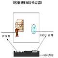
도 1은 일반적인 홀로그램 생성 원리를 나타낸 개략도로서, 도 1을 참조하면, 우선 물체(10)에 간섭성 광원인 레이저 광원(11)을 입사시켜 이로부터 반사 및 회절하는 빛, 즉, 물체파(12)를 감광 재료(13)에 입사시킨다. 그리고, 이와 동시에 레이저 광원(11)의 일부를 거울(14)을 통해서 상기 물체파(12)와 일정한 각도를 이루도록 하여 참조파(15)를 감광 재료(13)에 바로 입사시킨다. 여기서, 물체파(12)는 물체에 직접 부딪힌 후 반사 및 회절되어 서로 다른 위상을 가지고 재료에 부딪혀서 물체파(12)와 참조파(15)가 서로 간섭하여 감광재료 위에 미세한 간섭무늬를 남기게 된다. 상기 간섭무늬를 홀로그램이라고 하며, 홀로그램은 그 자체로는 대상의 물체를 닮지 않지만 물체에서 반사된 광선의 모든 위상과 세기에 대한 정보를 지닌다.FIG. 1 is a schematic diagram illustrating a general hologram generating principle. Referring to FIG. 1, first, an incident light of a
상기 홀로그램 기록과 반대로 기록된 영상을 재생하는 방법은, 홀로그램에 레이저 광선을 투과시키면 홀로그램 상의 미세한 간섭무늬들이 회절격자 역할을 하여 일부 광선을 회절시킴으로써 홀로그램을 생성한 광파의 원래 상태를 재현하게 되는바, 재현된 상은 원래 물체의 3차원적 특징들을 재현한 입체적 성질을 지니게 된다.In the method of reproducing the recorded image as opposed to the hologram recording, when the laser beam is transmitted to the hologram, fine interference patterns on the hologram act as a diffraction grating to diffract some rays to reproduce the original state of the light wave that generated the hologram. In other words, the reproduced image has three-dimensional properties that reproduce the three-dimensional characteristics of the original object.
이러한 홀로그램의 원리를 이용하여 실상 재현 기술을 통해 백색광 재생 기술을 통해 보안 목적의 홀로그램 생성 방법이 미국특허 제4,421,380호에 “완전 컬러 홀로그램(Full color hologram)"이라는 명칭으로 소개되어 있으며, 미국특허 제4,415,225호에 "홀로그래픽 이미지의 제조방법(Methods of making holographic images)"라는 명칭으로 소개되어 있다.The hologram generation method for security purposes through the white light reproduction technology through the actual reproduction technology using the holographic principle is introduced in the US Patent No. 4,421,380 under the name "Full color hologram", US Patent No. 4,415,225, entitled "Methods of making holographic images."
또한 2차원 평면의 홀로그램 무늬가 간단히 싸인(sin)파 형태로 표현된다는 것에 착안하여 그 회절 무늬를 표현하는 다른 방법이 미국특허 제5,132,812호에 “ 회절격자 패턴들을 갖는 이미지 형성 방법(Method of manufacturing display having diffraction grating patterns)"이라는 명칭으로 개시된바 있다.Another method of expressing the diffraction pattern in view of the fact that the hologram pattern of the two-dimensional plane is simply expressed in the form of a sin wave is described in US Patent No. 5,132,812 “Method of manufacturing display. having diffraction grating patterns).
이러한 홀로그램은 표면에 요철이 형성되므로 엠보스드 홀로그램이라고도 불리운다. 도 2는 이러한 홀로그램 표면의 일반적인 형상을 표현하였다.Such holograms are also called embossed holograms because irregularities are formed on the surface. 2 represents the general shape of this hologram surface.
도 3은 종래의 홀로그램 스티커의 기본 구조를 나타낸 도면으로서 스티커 형태의 라벨 기능을 한다. 도 4는 홀로그램 핫 스탬핑 포일로서 피착재와 접착시 열과 압력을 주어 PET 필름(film)을 박리하게 된다. 종래의 경우 은행권이나 유가증권에 홀로그래픽 스탬핑 포일을 부착하기 위한 별도의 부착공정과 고온 및 고압 상태의 부착기를 통하여 열 접착하여 보안라벨을 형성하였다.3 is a view showing the basic structure of a conventional hologram sticker to function as a label in the form of a sticker. FIG. 4 is a holographic hot stamping foil that exerts heat and pressure when adhering to an adherend to peel off a PET film. In the conventional case, a security label was formed by heat bonding through a separate attachment process for attaching the holographic stamping foil to banknotes or securities, and a high temperature and high pressure attacher.
따라서, 기존의 방법은 홀로그램을 제작하기 위해 스탬퍼를 제작하는 원판제조 공정과 더불어 홀로그램 스탬핑 포일을 제조하는 제조 라인이 필요하며 이를 통해 만들어진 홀로그램 스탬핑 포일을 별도의 부착 제조 시설을 통하여 은행권이나 유가 증권 위에 부착함으로써 제작이 번거로워지며 시간과 경비가 크게 소요되는 단점이 있다. 또한 별도의 부착 시설의 경우 용지를 급지하며 일정한 부위에 부착을 하여야 하므로 설비가 복잡해지며 도큐먼트의 일정한 위치에 정합하여 부착하는 번거로움으로 인하여 부착 경비가 많이 발생하게 되어 은행권 제조의 비용이 올라가며 보안 관리의 문제점이 발생할 수 있다.Therefore, the conventional method requires a manufacturing line for manufacturing hologram stamping foils in addition to a disc manufacturing process for manufacturing a stamper to produce holograms, and the hologram stamping foils thus produced are placed on banknotes or securities through a separate attachment manufacturing facility. By attaching, manufacturing is cumbersome and takes a lot of time and money. In addition, in the case of a separate attachment facility, paper is fed and attached to a certain part, which makes the facility complicated, and the installation cost is increased due to the hassle of matching and attaching to a certain location of the document. A problem may occur.
이에 본 발명에서는 대량의 홀로그램 스탬핑 포일을 생산하는 과정과 복잡하 고 번거롭게 부착하는 공정이 없이도 홀로그램, DOVID(Diffractive optical variable images device), 마이크로 렌즈 어레이, 재귀반사 프리즘 구조 또는 렌티큐러 렌즈의 형상 등의 미세 광학 요소를 은행권, 유가증권 등의 보안 도큐먼트에 부가하여 상술한 문제점을 해결할 수 있었고, 본 발명은 이에 기초하여 완성되었다.Therefore, in the present invention, a hologram, diffractive optical variable images device (DOVID), a micro lens array, a retroreflective prism structure, or the shape of a lenticular lens are produced without a process of producing a large amount of hologram stamping foil and a complicated and cumbersome attaching process. The above-mentioned problem could be solved by adding the micro-optical element of to banknotes, security documents, etc., and the present invention was completed based on this.
따라서, 본 발명의 목적은 스탬핑 포일이 없는 상태에서도 요판 인쇄 공정을 거친 후에는 특정 부위에 미세 광학 요소가 부가된 보안 도큐먼트를 제공하는 데 있다.Accordingly, an object of the present invention is to provide a security document in which a fine optical element is added to a specific portion after the intaglio printing process even in the absence of a stamping foil.
본 발명의 다른 목적은 요판 인쇄 공정에서 보안 도큐먼트에 직접적으로 미세 광학 요소를 부가할 수 있는 장치에 의해 광가변 요소가 부가된 보안 도큐먼트를 제조하는 방법을 제공하는 데 있다.Another object of the present invention is to provide a method for manufacturing a security document to which the optical variable element is added by an apparatus capable of adding a micro optical element directly to the security document in the intaglio printing process.
상기 목적을 달성하기 위한 본 발명에 따른 요판 인쇄 공정에 의해 광가변 요소가 부가된 보안 도큐먼트는 요판 인쇄 공정에 의해 제조되는 보안 도큐먼트에 있어서, 상기 도큐먼트의 적어도 한 부분에 인쇄된 수상층 상에 미세 광학 요소가 도입된 것으로 구성된다.The security document to which the optical variable element is added by the intaglio printing process according to the present invention for achieving the above object is a fine document on the water layer printed on at least one portion of the document in the security document produced by the intaglio printing process It consists of the introduction of an optical element.
본 발명의 다른 목적을 달성하기 위한 요판 인쇄 공정에 의해 보안 도큐먼트를 제조방법은 상기 도큐먼트의 적어도 한 부분에 수상층을 인쇄하는 단계; 미세 요철 구조가 삽입된 요판 인쇄용 원판을 제공하는 단계; 및 상기 요판 인쇄용 원판으로 상기 수상층 상에 미세 광학 요소를 도입시키는 단계;를 포함한다.According to another aspect of the present invention, there is provided a method of manufacturing a security document by an intaglio printing process, the method including: printing an aqueous layer on at least one portion of the document; Providing a disc for intaglio printing into which a fine concavo-convex structure is inserted; And introducing a fine optical element onto the water phase layer into the intaglio printing disc.
이하 본 발명을 첨부된 도면을 참조하여 좀 더 구체적으로 설명하면 다음과 같다.Hereinafter, the present invention will be described in more detail with reference to the accompanying drawings.
본 발명에서는 은행권이나 유가증권 등의 보안 도큐먼트에 요판 인쇄 공정을 통하여 도드라지는 인쇄를 한다는 점에 착안하여 이 요판 인쇄 공정시 상기 보안 도큐먼트에 홀로그램, DOVID, 마이크로 렌즈 어레이, 재귀반사 프리즘 구조 또는 렌티큐러 렌즈의 형상 등의 미세 광학 요소를 부가시켰다.In the present invention, a security document such as banknotes or securities is printed through the intaglio printing process, and the holographic, the DOVID, the microlens array, the retroreflective prism structure, or the lenticcue is applied to the security document during the intaglio printing process. And fine optical elements such as the shape of the lens.
본 발명에 따르면, 상기 보안 도큐먼트에 미세 광학 요소의 미세 표면 요철(Micro surface relief pattern)의 형성이 가능하도록 특별히 고안된 요판 인쇄용 종판을 고안하여 미세 광학 요소를 종판의 특정 부위에 삽입하도록 하여 요판 인쇄 공정시 자동적으로 도큐먼트의 특정 부위에 선택적으로 상기 미세 광학 요소의 형상이 삽입되도록 하였다.According to the present invention, the intaglio printing process by inventing the end plate for intaglio printing specifically designed to enable the formation of a micro surface relief pattern of the micro optical element in the security document to insert the micro optical element in a specific portion of the end plate Automatically allowing the shape of the micro-optical element to be selectively inserted into specific portions of the document.
즉, 요판 인쇄용 원판의 특정 부위에 광학적으로 변화하는 홀로그램이나 표면 요철 형상을 가지는 요소를 삽입한 후 요판 인쇄기에 장착한 후 요판 인쇄를 함으로서 요판 인쇄와 동시에 광학적으로 변화하는 요소를 생성하도록 하였다.That is, by inserting an element having an optically changing hologram or surface concave-convex shape in a specific portion of the intaglio printing disc and mounting it on the intaglio printing machine and then intaglio printing to generate an optically changing element at the same time as the intaglio printing.
이때 상기 미세 광학 요소의 형상이 부가된 부위는 그라비아 인쇄 또는 실크스크린 인쇄된 수상층(Acceptable functional layer)으로 먼저 코팅된다. 상기 수상층은 아크릴수지, 멜라민수지, 우레탄수지 등과 같은 수지(resin)이며, 알루미늄, 구리, 황화아연과 같은 금속층을 박막 코팅할 수 있다. 상기 수상층이 수지인 경우는 그라비아 인쇄 또는 실크스크린 인쇄 등으로 보안 도큐먼트에 코팅되며, 상기 수지층이 금속인 경우는 진공증착 코팅, 스탬핑 포일 부착 등으로 보안 도큐먼트에 부착될 수 있다.In this case, the portion to which the shape of the microscopic optical element is added is first coated with an gravure printed or silkscreen printed aqueous layer. The aqueous layer may be a resin such as an acrylic resin, melamine resin, urethane resin, or the like, and may be a thin film coating of a metal layer such as aluminum, copper, or zinc sulfide. The resin layer may be coated on the security document by gravure printing or silk screen printing, and the resin layer may be attached to the security document by vacuum deposition coating, stamping foil, or the like.
본 발명에 있어서, 상기 미세 광학 요소는 홀로그램, DOVID 등의 미세 회절 광학 요소와 마이크로 렌즈 어레이, 재귀반사 프리즘 구조 또는 렌티큐러 렌즈의 형상 등의 미세 굴절 요소로 구분된다. 이러한 미세 광학 요소는 보안 도큐먼트에 1종 이상이 도입될 수 있다.In the present invention, the fine optical element is divided into fine diffractive optical elements such as holograms and DOVIDs, and fine refractive elements such as the shape of a micro lens array, a retroreflective prism structure, or a lenticular lens. One or more of these microscopic optical elements may be introduced into a security document.
한편, 요판 인쇄용 종판의 제작 과정을 살펴보면, 일반적으로 요판 인쇄용 원판의 제작을 위하여는 조각 칼 등을 이용하여 강판, 동판, 황동판, 아연판 등의 판재에 윤곽 인쇄를 하고 싶은 부위를 선택적으로 파내는 1차 원판의 제작 공정이 있으며, 이렇게 제작된 1차 원판을 고분자 재질의 기판에 고온과 고압을 가하여 전이시킴으로서 1차 복제 플라스틱판을 제조한다. 이 1차 복제 플라스틱판을 여러 개 제작한 후 이것을 연결시켜 붙임으로서 요판 인쇄기의 원판과 같은 크기의 다면 소부된 플라스틱 원판을 얻을 수 있으며 이를 다시 니켈 금속 도금을 하여 요판 인쇄용 원판을 제작하게 된다.On the other hand, when looking at the manufacturing process of the final plate for intaglio printing, generally in order to manufacture the original plate for intaglio printing, using a engraving knife or the like to selectively excavate the portion that you want to contour print on the plate, such as steel plate, copper plate, brass plate, zinc plate, etc. There is a manufacturing process of the original, and the primary replica prepared as described above to produce a primary replica plastic plate by transferring the high temperature and high pressure to the substrate of the polymer material. By making several primary replica plastic plates and attaching them together, a multi-faceted plastic disc of the same size as the original plate of the intaglio printing press can be obtained, and nickel metal plating is used again to prepare the intaglio printing disc.
이렇게 제작된 요판 인쇄용 니켈 금속원판을 원형의 실린더에 부착한 후 요판 조각이 형성된 특정 부위에 선택적으로 잉크를 바른 후 압과 열을 주어 반대면의 보안 도큐먼트에 윤곽 인쇄를 실시한다.The intaglio printing nickel metal disc thus prepared is attached to a circular cylinder, and then selectively ink is applied to a specific area where the intaglio fragment is formed, and then pressure and heat are applied to outline the security document on the opposite side.
본 발명에서는 상기 요판 인쇄용 니켈 금속원판에 홀로그램 형상과 같은 미세 광학 요소를 도입하기 위한 방법으로서 세 가지 방법을 고안하였다.In the present invention, three methods have been devised as a method for introducing a microscopic optical element such as a hologram shape into the nickel metal disc for intaglio printing.
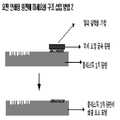
그 첫 번째 방법은 상술한 바와 같은 요판 인쇄용 원판을 제작함에 있어 1차 원판을 제작할 때 미세 광학 요소를 삽입할 부위를 일부 연마한 후 이 부위에 니켈 상태의 회절 요소 원판을 정합하여 삽입한 후 가장자리를 미세 용접을 통하여 부착시킨 다음 정교하게 연마를 한다. 이렇게 만들어진 원판으로 상술한 요판 인쇄용 원판 제작 과정을 거치게 되면 일정 부위에 광학 요소를 가지는 요판 인쇄용 원판을 제작할 수 있다. 도 5에 상기 과정을 간략히 나타내었다.The first method is to fabricate the disc for intaglio printing as described above, when manufacturing the primary disc, a part of the part to insert the micro-optical element is polished, and then the nickel diffraction element disc is matched and inserted into the edge. Is attached by fine welding and finely polished. When the original plate is thus subjected to the above-described intaglio printing disc manufacturing process, a disc for intaglio printing having an optical element on a predetermined portion can be produced. 5 shows the above process briefly.
두 번째 방법은 상기 요판 인쇄용 원판 제작 과정에서 1차 플라스틱 원판을 여러 개 제작한 후 특정 부위에 미세 광학 요소를 다시 각인하는 방법으로서 가장자리의 결함을 최소화할 수 있는 방법이 된다. 즉, 니켈 상태의 회절 광학 요소의 원판을 열과 압력을 주어 1차 플라스틱 원판의 특정 부위에 가해주면 미세 표면 형상이 전이됨을 이용하여 홀로그램 형상의 미세 광학 요소를 플라스틱 원판에 전이시킨 후 이 플라스틱 원판을 이어 붙임으로서 요판인쇄용 최종 원판을 만드는 방법이다. 도 6에 상기 과정을 간략히 나타내었다.The second method is a method of minimizing edge defects by manufacturing a plurality of primary plastic discs in the process of manufacturing the intaglio printing disc, and then again imprinting fine optical elements on specific portions. In other words, when the original plate of the diffractive optical element in the nickel state is applied to a specific part of the primary plastic disc by applying heat and pressure, the micro surface shape is transferred to transfer the holographic fine optical element to the plastic disc. It is then attached to make a final disc for intaglio printing. 6 shows the process briefly.
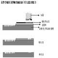
세 번째 방법으로서는 미세 식각 기술을 이용하여 요판 조각용 동판에 동판의 부식을 통하여 직접적으로 미세 광학 요소를 삽입하는 방법이 있다. 요판 조각용 강판에 감광제 등을 처리한 후 여기에 포토마스크를 장착하여 노광시켜 선택적으로 감광시킨 후 이를 현상하여 감광제를 벗겨낸 후 부식액에 동판을 부식시킴으로서 재귀반사 구조나 미세 프리즘, 렌티큐라 렌즈 등의 광학 요소를 표현하는 것이 가능하다. 도 7에 상기 과정을 간략히 나타내었다.As a third method, there is a method of directly inserting micro-optical elements through corrosion of the copper plate to the intaglio engraving copper plate using a fine etching technique. After processing the photoresist on the intaglio engraving steel plate, it is equipped with a photomask to expose it and then selectively photosensitive.Then, it is developed to peel off the photoresist, and the copper plate is corroded to the corrosive solution. It is possible to express the optical element of. 7 shows the above process briefly.
미세 회절 요소나 미세 굴절 요소의 미세한 표면 요철 구조는 깊이 수백 나노미터에서 수 마이크로 미터의 나노 요소로서 표면의 평활도가 좋지 않은 일반적 인 보안 도큐먼트의 종이 자체에는 수용되지 못하는 특징이 있다. 따라서 보안 도큐먼트의 특정 부위에 이 요철 구조를 받아들일 수 있도록 처리할 필요성이 있으며 이를 위해 본 발명에서는 그라비아 인쇄 또는 실크스크린 인쇄에서 두께 수 마이크로 미터의 화학 수지를 인쇄한 후 이 부분이 미세 광학 요소의 표면 요철 구조를 수용하도록 고안하였다.The fine surface irregularities of the fine diffractive element or fine refractive element are nanoelements of several hundred nanometers to several micrometers in depth and are not acceptable to the paper itself of a general security document with poor surface smoothness. Therefore, there is a need to treat the concave-convex structure in a specific part of the security document so that in the present invention, after printing a chemical resin having a thickness of several micrometers in gravure printing or silkscreen printing, the portion of the fine optical element It is designed to accommodate surface irregularities.
본 발명의 바람직한 일 실시예에 따르면, 실크스크린 인쇄 공정에서 미세 요철 구조의 광 보안 요소를 삽일할 부위에 굴절률이 1.5 이상되는 무색 또는 유색의 자외선 경화 물질을 2∼10㎛ 정도 인쇄하고 경화시킨다. 이렇게 형성된 부분은 홀로그램과 같은 미세 회절 광학 요소 뿐만 아니라 마이크로 렌즈 어레이, 재귀 반사 프리즘, 렌티큐라 렌즈 등의 미세 굴절 광학 요소들을 삽입하는 것이 가능하여 새로운 광 보안 요소로서 기능성을 가지게 하는 것이 가능하다.According to a preferred embodiment of the present invention, a colorless or colored ultraviolet curable material having a refractive index of 1.5 or more is printed and cured about 2 to 10 μm on a portion where the optical security element of the fine concavo-convex structure is inserted in the silk screen printing process. The portion thus formed is capable of inserting not only fine diffractive optical elements such as holograms, but also fine refractive optical elements such as micro lens arrays, retroreflective prisms, lenticular lenses, and so on, making it possible to have functionality as a new optical security element.
이하 실시 예를 통하여 본 발명을 좀 더 구체적으로 살펴보지만, 하기 예에 본 발명의 범주가 한정되는 것은 아니다.Hereinafter, the present invention will be described in more detail with reference to the following examples, but the scope of the present invention is not limited to the following examples.
실시 예 1Example 1
-종판의 제조 과정(홀로그램 도입)-Production process of final plate (hologram introduction)
전자빔 설비를 이용하여 깊이 100㎚, 간격 700㎚, 800㎚ 및 1000㎚의 홀로그램을 설계하여 금속원판을 제작하였으며 제작된 원판을 통해 두께 50㎛의 Ni 금속판을 제작 후 요판 종판의 특정 부위를 60㎛ 정도의 홀을 생성 후, 이에 미세 웰딩을 통해 부착하여 인쇄판을 제작하였다.A metal disc was fabricated by designing a hologram with a depth of 100 nm, an interval of 700 nm, 800 nm, and 1000 nm using an electron beam facility. A 50 μm thick Ni metal plate was fabricated through the fabricated disc, and then a specific portion of the intaglio end plate was 60 μm. After generating a degree of holes, it was attached through the fine welding to produce a printing plate.
-도큐먼트(유가증권)에 실크스크린 인쇄과정Silkscreen printing on documents (securities)
유가증권용 도큐먼트에 특정부위에 실크스크린 인쇄 공정을 통하여 UV 레진(Kayarad R-604, 일본화학)과 펜타데카플루오로옥틸메타크릴레이트(Penta deca fluoro octyl methacrylate)의 비율을 2:1로 조성한 레진을 노광량 100mj/㎠ 정도로 경화시켜 수지층을 형성하였다.Resin with a 2: 1 ratio of UV resin (Kayarad R-604 (Japan Chemical)) and penta deca fluoro octyl methacrylate through a silkscreen printing process on a specific part of a document for securities. Was cured at an exposure dose of about 100 mj / cm 2 to form a resin layer.
-상기 요판 인쇄용 원판으로 상기 수상층 상에 미세 광학 요소를 도입시키는 과정Introducing a micro-optical element on the water phase layer into the intaglio printing disc;
위와 같이 형성된 원판을 요판 인쇄 공정의 원판으로 장착 후 보안 도큐먼트를 요판 인쇄공정을 통하여 요판인쇄와 동시에 광가변 요소인 전자빔 식각에 의한 홀로그램이 생성됨을 확인하게 되었다.After mounting the disc formed as the disc of the intaglio printing process, the security document was confirmed through the intaglio printing process, and the hologram was generated by the electron beam etching which is the optical variable element at the same time as the intaglio printing process.
실시 예 2Example 2
초기 원판제작시 두께 50㎛, 원의 지름 30 ㎛ 정도의 원뿔 구조의 재귀반사 마이크로 렌즈 어레이를 싱글빔 레이저 식각을 통하여 제작한 후 나머지는 실시예 1과 같이 행함으로서 보안문서의 특정부위가 재귀반사 특징을 가지도록 실시하였다.Retro-reflective micro-lens array of conical structure with a thickness of 50 µm and a diameter of 30 µm at the time of initial fabrication was fabricated by single beam laser etching, and the rest was carried out as in Example 1 so that a specific part of the security document was retroreflected. It carried out to have a characteristic.
실시 예 1을 통하여 생성된 광보안 요소는 보안 도큐먼트에 삽입되어진 후 회절 효율이 14∼20% 정도로 관측됨으로써 육안으로 식별 가능한 위조 방지 요소임을 확인하였으며, 실시 예 2를 통하여 생성된 재귀반사 요소의 경우 정면의 수직입사각에서 약 20°기울어진 입사빔을 60∼70% 정도 재귀반사시킴으로써 육안 관측시 구별되며 컬러 복사시 표현이 불가능함을 확인할 수 있다.After the optical security element generated in Example 1 was inserted into the security document, the diffraction efficiency was observed to be about 14 to 20%, and thus it was confirmed that it was an anti-counterfeiting element visually identifiable. In the case of the retroreflective element generated through Example 2 By retroreflecting about 20-70% of the incident beam tilted at about 20 ° from the vertical incidence of the front face, it can be distinguished during visual observation and can not be expressed in color copying.
전술한 바와 같이, 본 발명에 따라 미세 광학 요소가 적용된 요판 인쇄용 종판을 1회 제작하여 이를 이용 수회 반복하여 도큐먼트의 일정 부위에 미세 광학 요소를 삽입하는 것이 가능해지므로 경제적이고도 간단하게 은행권 또는 유가증권 등을 위조로부터 보호하는 것이 가능해지며 별도의 홀로그램 포일이나 스티커가 필요 없이 홀로그램 보안 요소를 각종 유가증권상에 편리하게 삽입할 수 있는 혁신적인 방법이며 동시에 홀로그램 포일의 보관에 따른 유출의 위험을 극소화할 수 있다.As described above, according to the present invention, since the endplate for intaglio printing to which the micro-optical element is applied can be manufactured once and repeatedly used, it is possible to insert the micro-optical element into a certain portion of the document economically and simply, such as banknotes or securities. Can be protected from counterfeiting and the hologram security element can be conveniently inserted into various securities without the need for a separate hologram foil or sticker.At the same time, the risk of spillage due to the storage of the hologram foil can be minimized. .
또한, 홀로그램과 같은 회절 광학 요소 외에 마이크로 렌즈 어레이 등의 표면 요철 구조를 가지는 미세 굴절 요소를 은행권 등의 보안 도큐먼트에 삽입하는 것이 가능하므로 부가적인 보안요소의 생성이 가능하다.In addition, since it is possible to insert a fine refractive element having a surface concave-convex structure such as a micro lens array in addition to a diffractive optical element such as a hologram into a security document such as a banknote, it is possible to generate an additional security element.
Claims (11)
Translated fromKoreanPriority Applications (1)
| Application Number | Priority Date | Filing Date | Title |
|---|---|---|---|
| KR1020060025385AKR100817375B1 (en) | 2006-03-20 | 2006-03-20 | Security document with the optical variable element added by intaglio printing process and its manufacturing method |
Applications Claiming Priority (1)
| Application Number | Priority Date | Filing Date | Title |
|---|---|---|---|
| KR1020060025385AKR100817375B1 (en) | 2006-03-20 | 2006-03-20 | Security document with the optical variable element added by intaglio printing process and its manufacturing method |
Publications (2)
| Publication Number | Publication Date |
|---|---|
| KR20070095108A KR20070095108A (en) | 2007-09-28 |
| KR100817375B1true KR100817375B1 (en) | 2008-03-27 |
Family
ID=38688532
Family Applications (1)
| Application Number | Title | Priority Date | Filing Date |
|---|---|---|---|
| KR1020060025385AExpired - Fee RelatedKR100817375B1 (en) | 2006-03-20 | 2006-03-20 | Security document with the optical variable element added by intaglio printing process and its manufacturing method |
Country Status (1)
| Country | Link |
|---|---|
| KR (1) | KR100817375B1 (en) |
Citations (4)
| Publication number | Priority date | Publication date | Assignee | Title |
|---|---|---|---|---|
| US5783275A (en)* | 1993-05-01 | 1998-07-21 | Giesecke & Devrient Gmbh | Antifalsification paper |
| JP2002019259A (en)* | 2000-07-10 | 2002-01-23 | Shiseido Co Ltd | Material for preventing forgery and alteration |
| KR200338982Y1 (en)* | 2003-11-04 | 2004-01-24 | 주식회사 라임텍 | Security Hologram Film Having Water Mark and Filter |
| JP2004122642A (en)* | 2002-10-03 | 2004-04-22 | Konica Minolta Holdings Inc | Method for creating identification card for certification and transfer foil for protecting surface of card used for this method |
- 2006
- 2006-03-20KRKR1020060025385Apatent/KR100817375B1/ennot_activeExpired - Fee Related
Patent Citations (4)
| Publication number | Priority date | Publication date | Assignee | Title |
|---|---|---|---|---|
| US5783275A (en)* | 1993-05-01 | 1998-07-21 | Giesecke & Devrient Gmbh | Antifalsification paper |
| JP2002019259A (en)* | 2000-07-10 | 2002-01-23 | Shiseido Co Ltd | Material for preventing forgery and alteration |
| JP2004122642A (en)* | 2002-10-03 | 2004-04-22 | Konica Minolta Holdings Inc | Method for creating identification card for certification and transfer foil for protecting surface of card used for this method |
| KR200338982Y1 (en)* | 2003-11-04 | 2004-01-24 | 주식회사 라임텍 | Security Hologram Film Having Water Mark and Filter |
Also Published As
| Publication number | Publication date |
|---|---|
| KR20070095108A (en) | 2007-09-28 |
Similar Documents
| Publication | Publication Date | Title |
|---|---|---|
| AU2008263629B2 (en) | Holographic security device | |
| EP1782108B1 (en) | A method of creating a three-dimensional image, a diffractive element and method of creating the same | |
| US6975765B2 (en) | Optically variable form birefringent structure and method and system and method for reading same | |
| EA012512B1 (en) | A security device and method of manufacturing thereof | |
| US10710392B2 (en) | Diffractive security device and method of manufacture thereof | |
| MX2012010975A (en) | Security document with integrated security device and method of manufacture. | |
| JP5163137B2 (en) | Display body and article with display body | |
| GB2562797A (en) | Security device and method | |
| JP5504732B2 (en) | Display and labeled goods | |
| RU2431571C2 (en) | Optically changing protective device | |
| JP5321804B2 (en) | Diffraction grating | |
| JP4416161B2 (en) | Light diffraction structure | |
| JP5381445B2 (en) | 3D display image consisting of fine lines | |
| KR100817375B1 (en) | Security document with the optical variable element added by intaglio printing process and its manufacturing method | |
| JPH07320014A (en) | Information recording medium and manufacturing method thereof | |
| JP4910599B2 (en) | Diffraction structure transfer foil and method of manufacturing anti-counterfeit medium | |
| RU2642535C1 (en) | Multilayer protective element and method of its obtaining | |
| JP2013020084A (en) | Display body with computer-generated hologram, and labeled article | |
| JP4788910B2 (en) | Holographic anisotropic reflection composite medium | |
| KR20130010301A (en) | Anti-counterfeit hologram film having watermark have recorded thoreon multiple images, manufacturing method thereof and method for detection of watermark | |
| JP5935429B2 (en) | Identification method of anti-counterfeit media | |
| JP5644077B2 (en) | Authenticity identifier, authenticity determination sheet, and authenticity determination method | |
| JP5589268B2 (en) | Relief type diffraction grating or hologram | |
| JP5447819B2 (en) | Authenticity identifier | |
| JP5412773B2 (en) | Diffraction grating or hologram |
Legal Events
| Date | Code | Title | Description |
|---|---|---|---|
| A201 | Request for examination | ||
| PA0109 | Patent application | St.27 status event code:A-0-1-A10-A12-nap-PA0109 | |
| PA0201 | Request for examination | St.27 status event code:A-1-2-D10-D11-exm-PA0201 | |
| E902 | Notification of reason for refusal | ||
| PE0902 | Notice of grounds for rejection | St.27 status event code:A-1-2-D10-D21-exm-PE0902 | |
| T11-X000 | Administrative time limit extension requested | St.27 status event code:U-3-3-T10-T11-oth-X000 | |
| T11-X000 | Administrative time limit extension requested | St.27 status event code:U-3-3-T10-T11-oth-X000 | |
| P11-X000 | Amendment of application requested | St.27 status event code:A-2-2-P10-P11-nap-X000 | |
| P13-X000 | Application amended | St.27 status event code:A-2-2-P10-P13-nap-X000 | |
| E902 | Notification of reason for refusal | ||
| PE0902 | Notice of grounds for rejection | St.27 status event code:A-1-2-D10-D21-exm-PE0902 | |
| T11-X000 | Administrative time limit extension requested | St.27 status event code:U-3-3-T10-T11-oth-X000 | |
| PG1501 | Laying open of application | St.27 status event code:A-1-1-Q10-Q12-nap-PG1501 | |
| E701 | Decision to grant or registration of patent right | ||
| PE0701 | Decision of registration | St.27 status event code:A-1-2-D10-D22-exm-PE0701 | |
| GRNT | Written decision to grant | ||
| PR0701 | Registration of establishment | St.27 status event code:A-2-4-F10-F11-exm-PR0701 | |
| PR1002 | Payment of registration fee | St.27 status event code:A-2-2-U10-U11-oth-PR1002 Fee payment year number:1 | |
| PG1601 | Publication of registration | St.27 status event code:A-4-4-Q10-Q13-nap-PG1601 | |
| PN2301 | Change of applicant | St.27 status event code:A-5-5-R10-R13-asn-PN2301 St.27 status event code:A-5-5-R10-R11-asn-PN2301 | |
| PN2301 | Change of applicant | St.27 status event code:A-5-5-R10-R13-asn-PN2301 St.27 status event code:A-5-5-R10-R11-asn-PN2301 | |
| PN2301 | Change of applicant | St.27 status event code:A-5-5-R10-R13-asn-PN2301 St.27 status event code:A-5-5-R10-R11-asn-PN2301 | |
| PR1001 | Payment of annual fee | St.27 status event code:A-4-4-U10-U11-oth-PR1001 Fee payment year number:4 | |
| FPAY | Annual fee payment | Payment date:20120127 Year of fee payment:5 | |
| PR1001 | Payment of annual fee | St.27 status event code:A-4-4-U10-U11-oth-PR1001 Fee payment year number:5 | |
| LAPS | Lapse due to unpaid annual fee | ||
| PC1903 | Unpaid annual fee | St.27 status event code:A-4-4-U10-U13-oth-PC1903 Not in force date:20130321 Payment event data comment text:Termination Category : DEFAULT_OF_REGISTRATION_FEE | |
| P22-X000 | Classification modified | St.27 status event code:A-4-4-P10-P22-nap-X000 | |
| PC1903 | Unpaid annual fee | St.27 status event code:N-4-6-H10-H13-oth-PC1903 Ip right cessation event data comment text:Termination Category : DEFAULT_OF_REGISTRATION_FEE Not in force date:20130321 | |
| R18-X000 | Changes to party contact information recorded | St.27 status event code:A-5-5-R10-R18-oth-X000 | |
| P22-X000 | Classification modified | St.27 status event code:A-4-4-P10-P22-nap-X000 | |
| P22-X000 | Classification modified | St.27 status event code:A-4-4-P10-P22-nap-X000 | |
| PN2301 | Change of applicant | St.27 status event code:A-5-5-R10-R13-asn-PN2301 St.27 status event code:A-5-5-R10-R11-asn-PN2301 | |
| R18-X000 | Changes to party contact information recorded | St.27 status event code:A-5-5-R10-R18-oth-X000 | |
| PN2301 | Change of applicant | St.27 status event code:A-5-5-R10-R13-asn-PN2301 St.27 status event code:A-5-5-R10-R11-asn-PN2301 | |
| R18-X000 | Changes to party contact information recorded | St.27 status event code:A-5-5-R10-R18-oth-X000 |