KR100816746B1 - Cladded read-write conductor for a pinned-on-the-fly soft reference layer - Google Patents
Cladded read-write conductor for a pinned-on-the-fly soft reference layerDownload PDFInfo
- Publication number
- KR100816746B1 KR100816746B1KR1020020017756AKR20020017756AKR100816746B1KR 100816746 B1KR100816746 B1KR 100816746B1KR 1020020017756 AKR1020020017756 AKR 1020020017756AKR 20020017756 AKR20020017756 AKR 20020017756AKR 100816746 B1KR100816746 B1KR 100816746B1
- Authority
- KR
- South Korea
- Prior art keywords
- ferromagnetic
- layer
- cladding
- read
- write
- Prior art date
- Legal status (The legal status is an assumption and is not a legal conclusion. Google has not performed a legal analysis and makes no representation as to the accuracy of the status listed.)
- Expired - Fee Related
Links
Images


Classifications
- G—PHYSICS
- G11—INFORMATION STORAGE
- G11C—STATIC STORES
- G11C11/00—Digital stores characterised by the use of particular electric or magnetic storage elements; Storage elements therefor
- G11C11/02—Digital stores characterised by the use of particular electric or magnetic storage elements; Storage elements therefor using magnetic elements
- G11C11/14—Digital stores characterised by the use of particular electric or magnetic storage elements; Storage elements therefor using magnetic elements using thin-film elements
- G11C11/15—Digital stores characterised by the use of particular electric or magnetic storage elements; Storage elements therefor using magnetic elements using thin-film elements using multiple magnetic layers
- G—PHYSICS
- G11—INFORMATION STORAGE
- G11C—STATIC STORES
- G11C11/00—Digital stores characterised by the use of particular electric or magnetic storage elements; Storage elements therefor
- G11C11/02—Digital stores characterised by the use of particular electric or magnetic storage elements; Storage elements therefor using magnetic elements
- G11C11/16—Digital stores characterised by the use of particular electric or magnetic storage elements; Storage elements therefor using magnetic elements using elements in which the storage effect is based on magnetic spin effect
- B—PERFORMING OPERATIONS; TRANSPORTING
- B82—NANOTECHNOLOGY
- B82Y—SPECIFIC USES OR APPLICATIONS OF NANOSTRUCTURES; MEASUREMENT OR ANALYSIS OF NANOSTRUCTURES; MANUFACTURE OR TREATMENT OF NANOSTRUCTURES
- B82Y10/00—Nanotechnology for information processing, storage or transmission, e.g. quantum computing or single electron logic
- H—ELECTRICITY
- H10—SEMICONDUCTOR DEVICES; ELECTRIC SOLID-STATE DEVICES NOT OTHERWISE PROVIDED FOR
- H10B—ELECTRONIC MEMORY DEVICES
- H10B61/00—Magnetic memory devices, e.g. magnetoresistive RAM [MRAM] devices
Landscapes
- Engineering & Computer Science (AREA)
- Chemical & Material Sciences (AREA)
- Nanotechnology (AREA)
- Computer Hardware Design (AREA)
- Physics & Mathematics (AREA)
- Mathematical Physics (AREA)
- Theoretical Computer Science (AREA)
- Crystallography & Structural Chemistry (AREA)
- Mram Or Spin Memory Techniques (AREA)
- Hall/Mr Elements (AREA)
- Semiconductor Memories (AREA)
Abstract
Translated fromKoreanDescription
Translated fromKorean도 1은 기핀 고정 자화 배향을 갖는 기준층을 구비하는 종래의 자기 메모리 셀을 예시하는 도면,1 illustrates a conventional magnetic memory cell having a reference layer having a pinned pinned magnetization orientation;
도 2a 및 도 2b는 도 1의 종래의 자기 메모리 셀의 기준층과 데이터층 사이의 전체 평행 및 반평행 자화 배향을 각기 예시하는 도면,2A and 2B illustrate the total parallel and antiparallel magnetization orientations between the reference layer and the data layer of the conventional magnetic memory cell of FIG. 1, respectively;
도 2c 및 도 2d는 종래의 자기 메모리 셀에서 데이터층의 자화 배향에 대한 감자장의 영향을 예시하는 도면,2C and 2D illustrate the influence of the potato field on the magnetization orientation of a data layer in a conventional magnetic memory cell,
도 3a 및 도 3b는 핀 고정층과 핀 고정되는 층을 포함하는 다층의 기준층을 갖는 종래의 자기 메모리 셀을 예시하는 도면,3A and 3B illustrate a conventional magnetic memory cell having a multilayer reference layer comprising a pinned layer and a pinned layer;
도 4a는 종래의 자기 메모리 셀 어레이와 열 및 행 도전체를 포함하는 종래의 자기 메모리에서 판독 동작과 기입 동작을 예시하는 도면,4A illustrates a read operation and a write operation in a conventional magnetic memory including a conventional magnetic memory cell array and column and row conductors;
도 4b는 선택된 종래의 자기 메모리 셀에 대한 판독 동작과 열 및 행 도전체에 흐르는 판독 전류에 의해 발생되는 자장을 예시하는 도면,4B illustrates a magnetic field generated by a read operation for selected conventional magnetic memory cells and a read current flowing in column and row conductors;
도 5는 본 발명에 따른 연성 강자성체 기준층과 완전히 클래드된 판독 기입 도전체를 갖는 자기 메모리 셀을 예시하는 도면,5 illustrates a magnetic memory cell having a read ferrite conductor fully clad with a flexible ferromagnetic reference layer in accordance with the present invention;
도 6은 본 발명에 따른 판독 동작 동안에 강자성체 클래딩 내에 실질적으로 포함되는 자장을 예시하는 도면,6 illustrates a magnetic field substantially contained within a ferromagnetic cladding during a read operation in accordance with the present invention;
도 7은 본 발명에 따른 완전히 클래드된 판독 기입 도전체와 연성 강자성체 기준층을 갖는 자기 메모리 셀의 어레이를 포함하는 메모리를 예시하는 도면,7 illustrates a memory including an array of magnetic memory cells having a fully clad read write conductor and a flexible ferromagnetic reference layer in accordance with the present invention;
도 8a 내지 도 9b는 본 발명에 따른 판독 동작 동안에 즉석 핀 고정되는 연성 강자성체 기준층을 예시하는 도면,8A-9B illustrate a soft ferromagnetic reference layer that is pinned instantaneously during a read operation in accordance with the present invention;
도 10a 내지 도 10f는 본 발명에 따른 완전 클래드된 판독 기입 도전체와 연성 강자성체 기준층을 갖는 자기 메모리 셀을 만드는 방법을 예시하는 도면,10A-10F illustrate a method of making a magnetic memory cell having a fully clad read write conductor and a flexible ferromagnetic reference layer in accordance with the present invention;
도 11은 본 발명에 따라 연성 강자성체 기준층을 갖고 강자성체 데이터층에 데이터 비트를 기입하는 제 1 도전체를 포함하는 자기 메모리 셀을 예시하는 도면,11 illustrates a magnetic memory cell having a flexible ferromagnetic reference layer and including a first conductor for writing data bits to a ferromagnetic data layer in accordance with the present invention;
도 12는 본 발명에 따라 선택된 자기 메모리 셀의 강자성체 데이터층에 데이터 비트를 기입하는 제 1 도전체와 연성 강자성체 기준층을 갖는 자기 메모리 셀들의 어레이를 포함하는 메모리를 예시하는 도면,12 illustrates a memory including an array of magnetic memory cells having a first conductor and a soft ferromagnetic reference layer for writing data bits into a ferromagnetic data layer of a magnetic memory cell selected in accordance with the present invention;
도 13a 및 도 13b는 본 발명에 따라 강자성체 클래딩을 갖는 연성 강자성체 기준층과, 강자성체 클래딩과 강자성체 캡층을 갖는 연성 강자성체 기준층의 상대적인 디멘젼을 각기 예시하는 도면,13a and 13b respectively illustrate the relative dimensions of a soft ferromagnetic reference layer having a ferromagnetic cladding and a soft ferromagnetic reference layer having a ferromagnetic cladding and a ferromagnetic cap layer, respectively;
도 14a 및 도 14b는 본 발명에 따른 판독 동작과 강자성체 데이터층의 변경 가능한 자화 배향을 회전시키는 전환 자장을 예시하는 도면.14A and 14B illustrate a switching magnetic field for rotating a read operation and a changeable magnetization orientation of a ferromagnetic data layer in accordance with the present invention.
도면의 주요 부분에 대한 부호의 설명Explanation of symbols for the main parts of the drawings
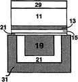
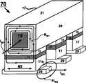
10 : 자기 메모리 셀11, 11a : 강자성체 데이터층10:
13 : 중간층15 : 강자성체 캡층13: intermediate layer 15: ferromagnetic cap layer
17 : 연성 강자성체 기준층19 : 판독 기입 도전체17: flexible ferromagnetic reference layer 19: read-write conductor
21 : 강자성체 클래딩29 : 제 1 도전체21: ferromagnetic cladding 29: the first conductor
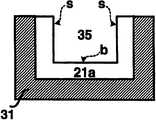
31 : 절연층33, 35 : 트렌치31:
50, 70 : 메모리
50, 70: memory
본 발명은 전반적으로 비-핀 고정 자화 배향(non-pinned orientation of magnetization)과 완전히 클래드된 기입-판독 도전체(wholly clad read-write conductor)를 포함하는 연성 강자성체 기준층(soft ferromagnetic reference layer)을 갖는 자기 메모리에 관한 것이다. 보다 구체적으로, 본 발명은 비-핀 고정 자화 배향을 갖고 강자성체 클래딩으로 완전히 둘러싸인 기입-판독 도전체를 포함하는 연성 강자성체 기준층을 갖는 자기 메모리 셀에 관한 것인데, 이렇게 강자성체 클래딩으로 완전히 둘러싸인 기입-판독 도전체는, 판독 기입 도전체에 흐르는 전류에 의해 발생된 판독 자장(read magnetic field)을 포화시키지 않고 강자성체 클래딩 내에 실질적으로 포함되게 하여, 자화의 배향이 메모리 셀에 대한 판독 동작 동안에 동적으로 즉석 핀 고정(dynamically pinned-on-the-fly)되도록 하며, 판독 기입 도전체에 흐르는 전류에 의해 발생되는 기입 자장(write magnetic field)은 강자성체 클래딩을 포화시켜서 강자성체 클래딩의 외부로 확장되어 하여 메모리 셀에 대한 기입 동작 동안에 데이터층과 상호 작용하게 한다.The present invention generally has a non-pinned orientation of magnetization and a soft ferromagnetic reference layer that includes a fully clad read-write conductor. It is about magnetic memory. More specifically, the present invention relates to a magnetic memory cell having a soft ferromagnetic reference layer having a non-pin pinned magnetization orientation and comprising a write-read conductor that is completely surrounded by a ferromagnetic cladding. The sieve allows the magnetization to be substantially contained within the ferromagnetic cladding without saturating the read magnetic field generated by the current flowing through the read-write conductor, so that the orientation of the magnetization is dynamically pinned dynamically during the read operation to the memory cell. write magnetic field generated by the current flowing through the read-write conductor, saturates the ferromagnetic cladding and extends out of the ferromagnetic cladding to write to the memory cell. Interact with the data layer during operation.
자기 임의 접근 메모리(MRAM)같은 자기 메모리는 DRAM, SRAM, 플래시 및 하드 디스크 드라이브같은 전통적인 데이터 기억 장치가 이용되는 애플리케이션에서 대체 데이터 기억장치로 여겨지는 비휘발성 메모리이다. MRAM은 전형적으로 자기 메모리 셀들로 이루어진 어레이를 포함한다. 예를 들어, 이전의 자기 메모리 셀은 데이터층(기억층 혹은 비트층으로 불리움), 기준층, 데이터층과 기준층 사이의 중간층을 포함하는 터널링 자기 저항 메모리 셀(TMR), 거대 자기 저항 메모리 셀(GMR) 혹은 초거대 자기 저항 메모리 셀(CMR)일 수 있다. 데이터층, 기준층 및 중간층은 하나 이상의 물질층으로 만들어질 수 있다. 데이터층은 흔히 자화의 배향으로서 데이터 비트를 기억하는 자기 물질의 층(layer) 혹은 막(film)인데, 이 자화의 배향은 외부 자기장의 인가에 응답하여 변경된다. 따라서, 데이터층의 자화의 배향(즉, 논리 상태)은 논리 "0"을 나타내는 자화의 처음 배향에서 논리 "1"을 나타내는 자화의 두 번째 배향으로 회전(즉, 전환)될 수 있거나, 혹은 그 반대로 회전될 수 있다. 한편, 기준층은 흔히 자화 물질의 층으로서, 이 층에서는 자화의 배향이 소정의 방향으로 "핀 고정(pinned)"(즉, 고정(fixed))된다. 이러한 사전 정의된 방향은 자기 메모리 셀을 제조하는데 이용되는 마이크로일렉트로닉 처리 단계에 의해 결정된다.Magnetic memory, such as magnetic random access memory (MRAM), is a nonvolatile memory that is considered an alternative data storage device in applications where traditional data storage devices such as DRAM, SRAM, flash, and hard disk drives are used. MRAM typically includes an array of magnetic memory cells. For example, previous magnetic memory cells may include a data layer (called a memory layer or a bit layer), a reference layer, a tunneling magnetoresistive memory cell (TMR) including an intermediate layer between the data layer and the reference layer, and a giant magnetoresistive memory cell (GMR). Or an ultra-large magnetoresistive memory cell (CMR). The data layer, reference layer, and intermediate layer can be made of one or more material layers. The data layer is often a layer or film of magnetic material that stores data bits as an orientation of magnetization, the orientation of the magnetization being changed in response to the application of an external magnetic field. Thus, the orientation of the magnetization of the data layer (ie, the logic state) can be rotated (ie, switched) from the initial orientation of the magnetization representing logic "0" to the second orientation of the magnetization representing logic "1", or It can be rotated in reverse. On the other hand, the reference layer is often a layer of magnetization material, in which the orientation of the magnetization is "pinned" (ie, fixed) in a predetermined direction. This predefined orientation is determined by the microelectronic processing steps used to fabricate magnetic memory cells.
전형적으로, 자기 메모리 셀의 논리 상태(즉, "0" 또는 "1")는 데이터층과 기준층의 상대적인 자화 배향에 따른다. 예를 들면, 터널링 자기 저항 메모리 셀(터널 접합 메모리 셀)에서, 전기 전위 바이어스가 데이터층과 기준층의 양단에 인가되면, 전자는 중간층(흔히 터널 장벽층으로 불리우는 박막의 절연층)을 통해 데이터층과 기준층 사이를 이동한다. 장벽층을 통한 전자의 이동을 초래하는 현상은 양자 역학적 터널링 혹은 스핀 터널링으로 언급될 수 있다. 논리 상태는 메모리 셀의 저항을 측정함으로써 결정될 수 있다. 예를 들어, 데이터 기억층의 전체 자화 배향이 기준층의 기핀 고정 자화 배향(pinned orientation of magnetization)과 평행하다면 자기 메모리 셀은 저 저항 상태(state of low resistance)이다. 반대로, 데이터 기억층의 전체 자화 배향이 기준층의 기핀 고정 자화 배향과 반평행(anti-parallel)하다면, 터널링 접합 메모리 셀은 고 저항 상태(state of high resistance)이다. 전술한 바와 같이, 자기 메모리 셀에 기억된 비트의 논리 상태는 데이터층의 전체 자화 배향을 변경하는 외부 자장을 인가함으로써 기입된다. 이러한 외부 자장은 자기 메모리 셀을 고 저항 상태와 저 저항 상태로 전환하는 전환 자장(switching fields)으로 불리울 수도 있다.Typically, the logic state (ie, "0" or "1") of the magnetic memory cell depends on the relative magnetization orientation of the data layer and the reference layer. For example, in a tunneling magnetoresistive memory cell (tunnel junction memory cell), when electrical potential bias is applied across the data layer and the reference layer, electrons pass through the intermediate layer (an insulating layer of a thin film, often called a tunnel barrier layer). Move between and the reference layer. The phenomenon causing the movement of electrons through the barrier layer may be referred to as quantum mechanical tunneling or spin tunneling. The logic state can be determined by measuring the resistance of the memory cell. For example, if the total magnetization orientation of the data storage layer is parallel to the pinned orientation of magnetization of the reference layer, the magnetic memory cell is in a state of low resistance. Conversely, if the total magnetization orientation of the data storage layer is anti-parallel with the pinned pinned magnetization orientation of the reference layer, the tunneling junction memory cell is in a state of high resistance. As described above, the logic state of the bits stored in the magnetic memory cell is written by applying an external magnetic field that changes the overall magnetization orientation of the data layer. This external magnetic field may be referred to as switching fields that switch magnetic memory cells into high and low resistance states.
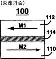
도 1은 데이터층(110), 기준층(112), 데이터층(110)과 기준층(112) 사이에 위치된 절연 장벽층(114)을 포함하는 종래의 터널링 접합 메모리 셀(100)을 예시한다. 또한, 메모리 셀(100)은 데이터층(110)과 접속된 제 1 전기 도전 노드(116)와, 기준층(112)과 접속된 제 2 전기 도전 노드(118)를 포함한다. 외부에서 공급된 전류는 제 1 및 제 2 전기 도전 노드(116, 118)를 통해 흘러서 전술한 외부 자장을 발생할 수 있다. 제 1 및 제 2 전기 도전 노드(116, 118)는 이후의 도 4a 및 도 4b에 논의될 다수의 메모리 셀(100)을 포함하는 메모리 어레이에서 열 및 행 도전체일 수 있다. 노드는 또한 메모리 셀(100)의 저항을 측정하여 그 논리 상태를결정하는데 이용될 수 있다. 기준층(112)은 좌향 화살표로 예시된 것과 같은 사전 정의된 방향으로 핀 고정된 자화 배향 M1을 갖는다. 데이터층(110)은 이중 화살표로 예시된 것과 같은 변경 가능한 자화 배향(alterable orientaion of magnetization) M2를 갖는다.1 illustrates a conventional tunneling
도 2a에서, 데이터층(110)의 자화 배향 M2는 기준층(112)의 자화 배향 M1과 평행(즉, 화살표가 동일 방향임)하고, 따라서 메모리 셀(100)은 저 저항 상태이다. 한편, 도 2b에서, 데이터층(110)의 자화 배향 M2는 기준층(112)의 자화 배향 M1과 반평행하고, 따라서 메모리 셀(100)은 고 저항 상태이다.In FIG. 2A, the magnetization orientation M2 of the
데이터층(110)과 기준층(112)은 서로 근접하여 위치된 강자성체 물질로 만들어졌기 때문에, 기준층(112)의 기핀 고정 자화 배향 M1은 도 2c에 예시된 바와 같이 기준층(112)의 에지 구역에서 데이터층(110)으로 뻗어 있는 감자장(demagnetization field) D을 발생한다. 도 2d는 데이터층(110)의 자화 배향 M2에 대한 감자장 D의 영향을 예시한다. 이상적으로는, 데이터층(110)의 자화 배향은 기핀 고정 자화 배향 M1에 평행하거나 반평행하게 정렬된다. 그러나, 감자장 D 때문에, 원래의 자화 배향 M2'(점선 화살표로 도시됨)와 실제 자화 배향 M2(실선 화살표로 표시됨) 사이에 작은 각도 변위 θ가 존재한다. 각도 변위 θ는 고 및 저 상태(즉, 평행 또는 반평행) 사이의 자기 저항 변화 ΔR/R의 크기를 감소시킨다. 자기 저항 변화의 크기는 가능한 한 커서, 데이터층(110)의 비트 상태 검출이 용이한 것이 바람직하다. 본질적으로, ΔR/R은 신호 대 잡음비 S/N과 마찬가지이다. 판독 동작 동안, 더 높은 S/N은 데이터층(110)의 비트 상태를 결정하기 위해 감지될 수 있는 더 강한 신호를 유발한다. 그러므로, 종래의 터널링 접합 메모리 셀(100)의 한 가지 단점은 각도 변위 θ로부터 초래되는 자기 저항 변화 ΔR/R의 크기 감소(즉, 판독 동작동안의 더 낮은 S/N)이다.Since the
종래의 터널링 접합 메모리셀(100)의 다른 단점은, 기준층(112)의 자화 배향 M1을 핀 고정하는 것이 종종 하나 이상의 물질층이 핀 고정을 실행하는 것을 필요로 한다는 것이다. 예를 들어, 도 3a에서, 종래의 터널링 접합 메모리 셀(200)은 전술한 데이터층(210), 제 1 및 제 2 전기 도전 노드(216, 218)를 포함하고, 또한 상이한 물질들의 샌드위치인 복합 기준층(212, 212a, 212b)를 포함한다. 층(212)은 반 강자성체체 층(antiferromagnet layer)(핀 고정층(pinning layer))이고, 층(212a)은 핀 고정되는 기준층(pinned reference layer)이다. 핀 고정층(212)은 기준층(212a)의 자화 배향 M1을 원하는 방향으로 자화한다. 층(212b)은 시드층(seed layer)이다. 핀 고정층(212), 기준층(212a), 시드층(212b)에 이용되는 물질의 예로서, 핀 고정층(212)에는 FeMn, IrMn, NiMn 혹은 PtMn을, 기준층(212a)에는 NiFe, NiFeCo 혹은 CoFe를, 시드층(212b)에는 NiFe 혹은 NiFeCo를 들 수 있다.Another disadvantage of conventional tunneling
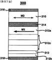
선택적으로, 도 3a에 도시된 것보다 더 복잡한 핀 고정층(312)를 갖는 종래의 터널링 접합 메모리 셀(300)이 도 3b에 예시된다. 종래의 터널링 접합 메모리 셀(300)은 전술한 데이터층(310)과 제 1 및 제 2 전기 도전 노드(316, 318)을 포함하고, 또한 상이한 물질들의 복합 샌드위치인 복합 기준층(312, 312a, 312b, 312c)을 포함한다. 핀 고정층(312)은 도 3a의 반 강자성체체 층(212)보다 훨씬 더 복잡한 구조를 갖는 인공 반 강자성체체(artificial antiferromagnet)(312c)의 자화 배향을 설정한다. 인공 반 강자성체체(312c)는 예컨대 Co/Ru/Co 혹은 CoFe/Ru/CoFe같은 물질의 샌드위치일 수 있다. 도 3b에서, 층(312a)은 핀 고정되는 기준층이고, 층(312b)은 시드층이고, 층(312)는 반 강자성체체 층(핀 고정층)이다.Optionally, a conventional tunneling
그러므로, 종래의 터널링 접합 메모리 셀의 한 가지 단점은, 기준층을 형성하기 위해 구조가 더 많은 층들을 필요로 한다는 것이다. 이들 층을 형성하는데 필요한 여분의 물질들 때문에, 종래의 터널링 접합 메모리 셀(200, 300)을 제조하는 데에는 여분의 마이크로일렉트로닉 처리 단계들이 필요하다. 이러한 여분의 단계들은 터널링 접합 메모리에 결함이 생길 가능성을 유발하여, 메모리가 제조될 때결함이 생기거나 혹은 이 메모리를 포함하는 제품에 추후의 장해를 일으킬 수 있다. 결함을 줄이고 수율을 증가시키기 위해서 복잡성 즉, 메모리를 제조하는데 필요한 처리 단계의 수를 최소화하는 것이 바람직하다. 더 나아가, 기준층을 형성하는데 필요한 물질들은 그 자체가 제조하기 어려운 물질들이다. 자기 메모리의 대량 생산을 위해, 제조 처리가 단순화되고 제조 비용이 감소되도록, 만들기 쉬운 물질을 이용하는 것이 바람직하다.Therefore, one disadvantage of conventional tunneling junction memory cells is that the structure requires more layers to form the reference layer. Because of the extra materials needed to form these layers, extra microelectronic processing steps are required to fabricate conventional tunneling
종래의 터널링 접합 메모리의 또 한가지 단점은, 기준층이 어닐링 단계에서 고온으로 열처리되어야 한다는 것이다. 어닐링은 시간이 걸리고(한 시간 이상) 자기 메모리가 일정한 자장하에서 200 내지 300℃의 온도로 처리되는 것을 필요로 한다. 자화의 배향을 설정하는 것은 자장에서의 어닐링을 요구하므로, 자기 메모리가 고온에서 이후에 처리될 경우, 기준층의 핀 고정이 "동요"되고 자화의 배향을 잃어버릴 가능성이 있다. 자화의 배향을 재설정하기 위해서, 다른 어닐링 단계가 요구될 수 있다.Another disadvantage of the conventional tunneling junction memory is that the reference layer must be heat treated at high temperature in the annealing step. Annealing takes time (more than an hour) and requires that the magnetic memory be treated at a temperature of 200-300 ° C. under a constant magnetic field. Setting the orientation of magnetization requires annealing in the magnetic field, so if the magnetic memory is subsequently processed at high temperatures, there is a possibility that the pinning of the reference layer is “swayed” and the orientation of the magnetization is lost. In order to reset the orientation of magnetization, another annealing step may be required.
종래 터널링 접합 메모리 셀(100)의 또 다른 단점은 도 4a, 4b, 4c에 예시된다. 도 4a에서, 자기 메모리(150)는 교차점 에레이로 구성된 다수의 메모리 셀(100)을 포함한다. 제 1 전기 도전 노드(116)는 메모리 셀(100)을 교차하는 열 도전체(Row1 및 Row2)를 형성하도록 반복되고, 제 2 전기 도전 노드(118)는 메모리 셀(100)을 교차하는 행 도전체(Col1, Col2, Col3)를 형성하도록 반복된다(즉, 메모리 셀(100)은 열과 행 도전체의 교차점에 위치된다). Row2와 Col3의 교차점에 위치된 메모리 셀(100a)은 판독 동작을 위해 Row1을 부동(floating) 상태로 둔 채로 전압원 V를 Row2에 접속함으로써 선택된다. Col1과 Col2는 접지되고, Col3은 가상 접지된 감지 증폭기 S에 접속된다. 결과적으로, 전류 경로가 형성되어, 전류 I가 Row2의 도전 노드(116)에 흐른다. 전류 I의 일부는 전류 IG로 표시된 바와 같이 접지로 흐른다. 그러나, 전류의 다른 부분은 감지 증폭기 S에 의해 감지되는 판독 전류 IR을 포함한다. IR의 크기는 메모리 셀(100)에 기억된 데이터 비트의 자화 배향의 표시이지만, IR의 크기가 판독 동작동안 데이터층의 자화 배향을 회전시킬 정도는 아니다.Another disadvantage of the conventional tunneling
도 4b에서, 선택된 메모리 셀(100a)이 더 자세히 도시된다. 전류 IR은 오른 손 법칙에 따라 자장 HR을 발생한다. 자신의 각 도전체로부터 밖을 향해 방사상으로 뻗어 나와 어레이내의 인접 메모리 셀(100)과 상호 작용하는 자장 HR(즉, 주변 기생 자장(fringe fields))로부터 단점이 발생한다. 서로에 대한 메모리 셀(100)의 인접도와 전류 IR의 크기에 따라서, 이러한 주변 기생 자장은 판독 동작에 선택되지 않은 인접한 메모리 셀(100)의 데이터층(100)에 기억된 데이터 비트를 파괴할 수 있다.In FIG. 4B, the selected
마찬가지로, Row1 및 Col3의 교차점에 위치된 메모리 셀(100b)은 Col3을 통해 전류 Ix를 통과시키고 Row1을 통해 전류 Iy를 통과시킴으로써 기입 동작에 선택된다. 전류 Ix및 Iy는 변경 가능한 자화 배향을 회전시키기 위해 데이터층과 협력적으로 상호작용하는 자장을 발생시켜 새로운 데이터 비트를 기입한다.Similarly,
도 4c에서, 선택된 메모리 셀(100b)이 더 상세히 도시된다. 전류 Iy는 오른손 법칙에 따라 자장 Hx를 발생한다. 마찬가지로, 전류 Ix는 오른손 법칙에 따라 자장 Hy를 발생한다. 각 도전체로부터 방사상으로 밖으로 뻗어 나와 선택된 메모리 셀(100b)에 대한 기입 동작 동안에 어레이내의 인접 메모리 셀(100)과 상호 작용하는 이들 자장들(즉, 주변 기생 자장)에 의해 단점이 발생한다. 서로에 대한 메모리 셀(100)의 인접도와 전류 Ix 및 Iy의 크기에 따라서, 이들 주변 기생 자장은 기입 동작에 선택되지 않은 인접 메모리 셀(100)의 데이터층(100)에 기억된 데이터 비트를 손상시킬 수 있다. 전류 Ix 및 Iy의 크기는 판독 동작에 대한 것보다는 기입 동작에 대한 것이 더 크기 때문에, 데이터 손상의 가능성은, 자화의 배향 을 회전시키기 위해 최종 자장이 데이터층까지 뻗어 있어야 하는 기입 동작동안에 더 커진다.In FIG. 4C, the selected
또한, 종래의 터널링 접합 메모리 셀(100)의 또 다른 단점은, 선택된 메모리 셀(100)에 데이터를 판독 및/또는 기입하는데 필요한 판독 전류 IR와 기입 전류 Ix 및 Iy의 크기가 상당히 클 수 있다(기입 전류는 통상적으로 판독 전류보다 더 크다)는 것이다. 이러한 전류들은 원치 않는 폐기열(waste heat)의 발생을 초래하여, 폐기열을 제거하기 위한 냉각 팬같은 열 관리 시스템이 요구될 수 있다. 열 관리 시스템은 메모리(150)을 포함하는 전자 시스템에 비용, 크기, 무게 및 잡음을 추가할 수 있다. 전력 공급원을 배터리에 의존하는 휴대용 전자 시스템이나 에너지가 효율적이도록 설계된 전자 시스템의 경우, 전술한 전류는 전력 소비를 가중시켜 배터리 수명을 단축시키거나 전력 낭비를 증가시켜 에너지 효율을 손상시킬 수 있다.Further, another disadvantage of the conventional tunneling
전술한 단점들이 터널링 접합 메모리 셀(즉, TMR 메모리 셀)에 초점을 맞춰 설명되었을지라도, 이 단점들은 예컨대 전술한 GMR 및 CMR 메모리 셀 같은 다른 유형의 자기 메모리 셀에도 똑같이 적용된다. 예를 들어, 종래에 공지된 바와 같이, GMR 메모리 어레이(도시 안됨)의 경우, 교차점 어레이는 GMR 메모리 셀들을 전기적으로 절연시키는 게이트 트랜지스터(즉, FET)로 대체된다. FET는 판독 동작을 위한 특정 GMR 셀을 선택하기 위해 전기적으로 온-오프가 전환된다. 선택된 메모리 셀에 흐르는 판독 전류는 감지 증폭기같은 것에 의해 감지될 수 있다.Although the foregoing disadvantages have been described focusing on tunneling junction memory cells (ie, TMR memory cells), these disadvantages apply equally to other types of magnetic memory cells such as the GMR and CMR memory cells described above, for example. For example, as is known in the art, in the case of a GMR memory array (not shown), the crosspoint array is replaced with a gate transistor (ie, a FET) that electrically insulates the GMR memory cells. The FET is electrically switched on and off to select a particular GMR cell for the read operation. The read current flowing to the selected memory cell can be sensed by something like a sense amplifier.
그러므로, 데이터층에 기억된 데이터 비트를 판독하기 위해 기핀 고정 자화 배향을 요구하지 않는 기준층을 갖는 자기 메모리 셀이 필요하다. 또한 기준층을 형성하는데 필요한 물질층의 수를 줄이는 것이 필요하다. 더 나아가, 판독 또는 기입 동작 동안에 발생된 주변 기생 자장이 실질적으로 기준층에 한정되어 인접 메모리 셀과의 간섭이 실질적으로 감소되는 자기 메모리 셀이 필요하다. 또한, 판독 또는 기입 동작을 실행하는데 필요한 전류의 크기가 감소되어 전력 소비와 전력 낭비가 줄어드는 자기 메모리 셀이 필요하다. 마지막으로, 데이터층의 자화 배향의 각도 변위가 실질적으로 감소되거나 제거되어, 판독 동작 동안 자기 저항의 변화의 크기가 보다 큰 자기 메모리 셀이 필요하다.Therefore, there is a need for a magnetic memory cell having a reference layer that does not require a pinned magnetization orientation to read the data bits stored in the data layer. It is also necessary to reduce the number of material layers needed to form the reference layer. Furthermore, there is a need for a magnetic memory cell in which a peripheral parasitic magnetic field generated during a read or write operation is substantially confined to the reference layer such that interference with adjacent memory cells is substantially reduced. There is also a need for a magnetic memory cell in which the magnitude of the current required to perform a read or write operation is reduced, thereby reducing power consumption and power waste. Finally, the angular displacement of the magnetization orientation of the data layer is substantially reduced or eliminated, so that a magnetic memory cell with a larger magnitude of change in magnetoresistance during a read operation is needed.
본 발명은 예컨대 터널링 자기 저항 메모리 셀(TMR), 거대 자기 저항 메모리 셀(GMR) 및, 이러한 유형의 자기 메모리 셀을 포함하는 메모리 같은 자기 메모리 셀의 설계를 개선하는 것이다. 더 나아가, 본 발명은 자기 메모리 셀의 기준층에 이용되는 물질과, 자기 메모리 셀의 판독 기입 도전체에 이용되는 구조를 개선하는 것이다.The present invention improves the design of magnetic memory cells, such as, for example, tunneling magnetoresistive memory cells (TMRs), giant magnetoresistive memory cells (GMRs), and memories comprising these types of magnetic memory cells. Furthermore, the present invention improves the material used for the reference layer of the magnetic memory cell and the structure used for the read-write conductor of the magnetic memory cell.
광의적으로, 본 발명은 데이터 비트를 변경 가능한 자화 배향으로서 기억하는 강자성체 데이터층과, 강자성체 데이터층과 전기적으로 통하는 제 1 도전체와, 강자성체 데이터층과 접촉하는 중간층과, 중간층과 접촉하며 판독 기입 도전체와 이 판독 기입 도전체를 완전히 둘러싸서 클래드형 판독 기입 도전체를 형성하는 강자성체 클래딩을 포함하는 연성 강자성체 기준층을 포함하는 자기 메모리 셀에 구현된다. 강자성체 클래딩은 필요에 따라 절단된 두께를 갖는데(즉, 어떤 영역의 두께는 더 두껍고 다른 영역의 두께는 더 얇은 단면적 두께를 갖는다), 중간층과 접촉하는 강자성체 클래딩의 일부분을 따라서는 박막 부분이고, 중간층과 접촉하지 않는 강자성체 클래딩의 부분을 따라서는 후막 부분이다. 연성 강자성체 기준층은 비-핀 고정 자화 배향을 갖는다(즉, 자화의 배향이 사전 정의된 한 방향으로 정해지지 않는다).Broadly speaking, the present invention provides a ferromagnetic data layer that stores data bits as a changeable magnetization orientation, a first conductor in electrical communication with the ferromagnetic data layer, an intermediate layer in contact with the ferromagnetic data layer, and an intermediate layer in contact with the intermediate layer. A magnetic memory cell comprising a conductor and a soft ferromagnetic reference layer comprising a ferromagnetic cladding that completely surrounds the read and write conductors to form a clad read write conductor. The ferromagnetic cladding has a cut thickness as needed (ie, the thickness of some regions is thicker and the thickness of other regions has a thinner cross-sectional thickness), which is a thin film portion along a portion of the ferromagnetic cladding in contact with the intermediate layer, Along the portion of the ferromagnetic cladding that is not in contact with it is the thick film portion. The soft ferromagnetic reference layer has a non-pin pinned magnetization orientation (ie, the orientation of magnetization is not defined in one predefined direction).
판독 동작 동안, 외부에서 공급된 전류는 판독 기입 도전체를 통해 흐르고, 판독 기입 도전체는 이 전류에 응답하여 판독 자장을 발생한다. 강자성체 클래딩은 판독 자장에 의해 포화되지 않으며, 판독 자장은 실질적으로 강자성체 클래딩(박막 부분 포함)내에 포함된다. 판독 자장의 결과, 연성 강자성체 기준층의 자화 배향은 원하는 방향으로 즉석에서 핀 고정된다. 강자성체 데이터층에 기억된 데이터 비트는 연성 강자성체 기준층과 제 1 도전체 사이의 저항을 측정함으로써 판독된다.During the read operation, an externally supplied current flows through the read write conductor, and the read write conductor generates a read magnetic field in response to this current. The ferromagnetic cladding is not saturated by the read magnetic field, and the read magnetic field is substantially contained within the ferromagnetic cladding (including the thin film portion). As a result of the read magnetic field, the magnetization orientation of the soft ferromagnetic reference layer is pinned immediately in the desired direction. The data bits stored in the ferromagnetic data layer are read by measuring the resistance between the soft ferromagnetic reference layer and the first conductor.
반대로, 기입 동작 동안, 제 1 기입 전류는 판독 기입 도전체를 통해 흘러서, 박막 부분을 따라 존재하는 강자성체 클래딩을 포화시키고, 강자성체 데이터층을 향하는 방향으로 강자성체 클래딩 밖으로 뻗어 나가는 제 1 자장을 발생하며, 제 2 기입 전류는 제 1 도전체를 통해 흘러서 마찬가지로 강자성체 데이터층으로 뻗어 나가는 제 2 기입 자장을 발생한다. 제 1 및 제 2 기입 자장은 강자성체 데이터층과 협력적으로 상호 작용하여, 변경 가능한 자화 배향을 회전시킴으로써, 강자성체 데이터층에 새로운 데이터 비트를 기입한다. 기입 동작 동안, 제 1 기입 자장은 강자성체 클래딩의 후막 부분을 포화시키지 않는다.Conversely, during a write operation, the first write current flows through the read write conductor, saturates the ferromagnetic cladding present along the thin film portion, and generates a first magnetic field that extends out of the ferromagnetic cladding in a direction towards the ferromagnetic data layer, The second write current flows through the first conductor and generates a second write magnetic field that likewise extends into the ferromagnetic data layer. The first and second write magnetic fields interact cooperatively with the ferromagnetic data layer to write new data bits into the ferromagnetic data layer by rotating the changeable magnetization orientation. During the write operation, the first write magnetic field does not saturate the thick film portion of the ferromagnetic cladding.
본 발명의 클래드형 판독 기입 도전체의 다른 이점은, 판독 동작 동안에 판독 기입 도전체로부터의 판독 자장이 강자성체 클래딩 내에 실질적으로 포함되므로 주변 기생 자장이 상당히 감소되며, 기입 동작 동안에 제 1 기입 자장을 실질적으로 강자성체 데이터층을 향하는 방향으로 이끌어 기입 동작 동안에 인접 메모리 셀과 상호 작용하는 주변 기생 자장이 실질적으로 감소될 수 있도록 강자성체 클래딩의 두께를 절단할 수 있다는 것이다.Another advantage of the clad type read write conductor of the present invention is that the read field from the read write conductor is substantially included in the ferromagnetic cladding during the read operation, so that the peripheral parasitic magnetic field is significantly reduced, and the first write magnetic field is substantially reduced during the write operation. In other words, the thickness of the ferromagnetic cladding can be cut so that the peripheral parasitic magnetic field interacting with adjacent memory cells during the write operation can be reduced in a direction toward the ferromagnetic data layer.
판독 동작 동안, 본 발명의 강자성체 클래딩은 판독 자장을 위한 폐쇄된 자속 경로(closed flux path)(자속 폐쇄(flux closure))를 제공한다. 그 결과, 종래의 자기 메모리 셀의 감자장이 실질적으로 감소되거나 제거되어 각도 변위가 최소화되고, 판독 동작 동안에 자기 저항에서 더 큰 변화의 크기가 존재한다. During the read operation, the ferromagnetic cladding of the present invention provides a closed flux path (flux closure) for the read magnetic field. As a result, the potato field of conventional magnetic memory cells is substantially reduced or eliminated so that angular displacement is minimized, and there is a greater magnitude of change in magnetic resistance during the read operation.
종래의 기핀 고정 기준층의 단점들은 본 발명의 연성 강자성체 기준층에 의해 해결되는데, 그 이유는, 판독 동작이 연성 강자성체 기준층의 자화 배향이 핀 고정되는 것을 필요로 하지 않기 때문이다. 대신에, 판독 동작을 실행하기 위해서, 사전정의된 크기와 방향의 전류를 판독 기입 도전체를 통해 통과시킴으로써 본 발명의 연성 강자성체 기준층의 자화 배향은 원하는 방향으로 동적으로 핀 고정된다(즉, 즉석에서 핀 고정된다). 결과적으로, 전술한 추가의 물질층, 이들 물질층의 복잡성, 이들 물질층을 형성하는데 필요한 마이크로일렉트로닉 처리 단계들이 감소된다. 본 발명의 연성 강자성체 기준층에 의해 자장내에서 기준층을 어닐링할 필요성이 제거된다. 더 나아가, 자화 배향이 동적으로 즉석에서 핀 고정되기 때문에, 메모리가 열처리될 경우에 기준층의 자화 배향이 "재설정(reset)"될 가능성도 본 발명의 연성 강자성체 기준층에 의해 작아진다.The disadvantages of the conventional pinned reference layer are solved by the flexible ferromagnetic reference layer of the present invention, since the read operation does not require the magnetization orientation of the flexible ferromagnetic reference layer to be pinned. Instead, in order to perform the read operation, the magnetization orientation of the flexible ferromagnetic reference layer of the present invention is pinned dynamically in the desired direction (i.e. on the fly) by passing a current of a predefined magnitude and direction through the read write conductor. Pin is fixed). As a result, the additional material layers described above, the complexity of these material layers, and the microelectronic processing steps required to form these material layers are reduced. The soft ferromagnetic reference layer of the present invention eliminates the need to anneal the reference layer in the magnetic field. Furthermore, since the magnetization orientation is pinned dynamically instantaneously, the likelihood that the magnetization orientation of the reference layer is "reset" when the memory is heat treated is also reduced by the soft ferromagnetic reference layer of the present invention.
본 발명의 자기 메모리 셀의 다른 이점은, 판독 혹은 기입 동작에 필요한 전류의 크기가 작아져서 전력 낭비(폐기열)와 전력 소모가 줄어든다는 것이다. 판독 또는 기입 동작을 위한 전류는 정적 dc 전류이거나 동적 전류 펄스일 수 있다. 전술한 바와 같이, 특히 배터리로 동작하는 휴대용 시스템과 어네지 효율 시스템에서는 전력 소모와 폐기열 발생을 최소화하는 것이 바람직하다.Another advantage of the magnetic memory cell of the present invention is that the amount of current required for a read or write operation is reduced, thereby reducing power waste (waste heat) and power consumption. The current for read or write operations can be a static dc current or a dynamic current pulse. As mentioned above, it is desirable to minimize power consumption and waste heat generation, especially in battery operated portable systems and energy efficient systems.
본 발명의 일 실시예에서, 자기 메모리 셀은 강자성체 클래딩과 증간층 사이에 위치하여 강자성체 클래딩과 자기적으로 결합되어 있는 강자성체 캡층(ferromagnetic cap layer)을 포함한다. 판독 동작 동안, 판독 자장은 포화되지 않으며, 실질적으로 강자성체 캡층과 강자성체 클래딩 내에 포함된다. 기입 동작 동안, 제 1 기입 자장은 강자성체 클래딩의 박막 부분과 강자성체 캡층을 포화시켜서 강자성체 데이터층을 향하는 방향으로 밖으로 뻗어 있다. 그러나, 제 1 기입 자장은 강자성체 클래딩의 후막 부분은 포화시키지 않는다.In one embodiment of the present invention, the magnetic memory cell includes a ferromagnetic cap layer positioned between the ferromagnetic cladding and the enrichment layer and magnetically coupled to the ferromagnetic cladding. During a read operation, the read magnetic field is not saturated and is substantially contained within the ferromagnetic cap layer and the ferromagnetic cladding. During a write operation, the first write magnetic field saturates the thin film portion of the ferromagnetic cladding and the ferromagnetic cap layer and extends out in the direction toward the ferromagnetic data layer. However, the first write magnetic field does not saturate the thick film portion of the ferromagnetic cladding.
본 발명의 다른 실시예에서, 강자성체 데이터층, 강자성체 캡층, 강자성체 클래딩은 높은 자기 투자율의 연성 자기 물질(high magnetic permeability soft magnetic material)로 만들어 질 수 있다. 본 발명의 또 다른 실시예에서, 강자성체 데이터층, 강자성체 캡층, 강자성체 클래딩은 동일한 높은 자기 투자율의 연성 자기 물질로 제조되는다.In another embodiment of the present invention, the ferromagnetic data layer, the ferromagnetic cap layer, and the ferromagnetic cladding may be made of high magnetic permeability soft magnetic material. In another embodiment of the invention, the ferromagnetic data layer, ferromagnetic cap layer, and ferromagnetic cladding are made of the same high magnetic permeability soft magnetic material.
본 발명의 일 실시예에서, 강자성체 데이터층, 강자성체 캡층, 강자성체 클래딩은 낮은 보자성 물질(low coercivity material)로 만들어 질 수 있다.In one embodiment of the present invention, the ferromagnetic data layer, the ferromagnetic cap layer, and the ferromagnetic cladding may be made of a low coercivity material.
본 발명의 선택적 실시예에서, 자기 메모리 셀은 터널링 자기 저항 메모리 셀이거나 혹은 거대 자기 저항 메모리 셀일 수 있다.In an optional embodiment of the invention, the magnetic memory cell may be a tunneling magnetoresistive memory cell or a giant magnetoresistive memory cell.
본 발명의 다른 측면들과 이점들은 본 발명의 원리를 예시하는 첨부 도면들과 연계하여 취해진 이후의 상세한 설명으로부터 명확해질 것이다.
Other aspects and advantages of the present invention will become apparent from the following detailed description taken in conjunction with the accompanying drawings which illustrate the principles of the invention.
다음의 상세한 설명과 몇몇 도면에서 동일한 요소들은 동일한 참조 번호로 식별된다.In the following description and in the drawings, like elements are identified by like reference numerals.
예시를 목적으로 한 도면에 도시된 바와 같이, 본 발명은 변경 가능한 자화 배향으로서 데이터 비트를 기억하는 강자성체 데이터층과, 강자성체 데이터층과 전기적으로 통신하는 제 1 도전체와, 강자성체 데이터층과 접촉하는 중간층과, 중간층과 접촉하며 판독 기입 도전체와 이 판독 기입 도전체를 완전히 둘러싸서 클래드형 판독 기입 도전체를 형성하는 강자성체 클래딩을 포함하는 연성 강자성체 기준층을 포함한다. 연성 강자성체 기준층은 사전 정의된 방향으로 기핀 고정되지 않은 자화 배향을 갖는다. 이후부터, 연성 강자성체 기준층의 특징은 "비-핀 고정 자화 배향"으로 언급될 것이다.As shown in the drawings for purposes of illustration, the present invention provides a contact between a ferromagnetic data layer storing data bits as a changeable magnetization orientation, a first conductor in electrical communication with the ferromagnetic data layer, and a contact with the ferromagnetic data layer. An intermediate layer and a soft ferromagnetic reference layer comprising a ferromagnetic cladding in contact with the intermediate layer and a ferromagnetic cladding that completely surrounds the read and write conductors to form a cladding read and write conductor. The soft ferromagnetic reference layer has a magnetization orientation that is not pinned in the predefined direction. From now on, the feature of the soft ferromagnetic reference layer will be referred to as the "non-pin pinned magnetization orientation."
판독 기입 도전체는 외부에서 공급된 판독 전류에 응답하여 판독 자장을 발생하고, 강자성체 클래딩은 실질적으로 강자성체 클래딩 내에 판독 자장을 포함한다. 필수적으로, 강자성체 클래딩은 판독 기입 도전체 둘레에 폐쇄 자기 경로(자속 폐쇄)를 제공한다. 사전 정의된 크기와 방향을 갖는 전류를 판독 기입 도전체에 통과시킴으로써 발생된 판독 자장은 연성 강자성체 기준층에 공지된 방향으로 자화 배향을 설정하기에 충분하고, 결국 자화 배향이 동적으로 핀 고정된다(즉, 자화 배향이 즉석에서 핀 고정된다). 그러나, 판독 자장이 연성 강자성체 기준층의 강자성체 클래딩을 포화시킬 정도로 충분하지는 않고, 판독 자장은 실질적으로 강자성체 클래딩의 밖으로 뻗어 나와 강자성체 데이터층에 기억된 데이터 비트와 혹시 간섭하거나 겹쳐쓰기(overwrite)를 할 수도 있다. 강자성체 클래딩은 또한 인접 메모리 셀의 강자성체 데이터층에 기억된 데이터와 간섭하거나 이 데이터를 손상시킬 수 있는 주변 기생 자장을 실질적으로 약화시킨다. 데이터 비트는 연성 강자성체 기준층과 제 1 도전체 사이의 저항을 측정함으로써 판독될 수 있다. 강자성체 클래딩과 강자성체 데이터층은 높은 자기 투자율의 연성 자기 물질로 만들어 질 수 있다. 강자성체 클래딩은 판독 자장이 강자성체 클래딩 내에 실질적으로 포함되도록 설계되어 절단된 두께를 갖는다. 그러나, 절단된 두께는 중간층과 접촉하는 강자성체 클래딩 부분을 따라서는 보다 박막인 부분을 포함하여, 기입 동작 동안에 제 1 기입 전류가 판독 기입 도전체를 통과하면, 이 박막 부분을 따라 강자성체 클래딩을 포화시키고 강자성체 데이터층을 향하는 방향으로 강자성체 클래딩의 밖으로 뻗어 나가는 제 1 기입 자장이 발생되어, 강자성체 데이터층에 새로운 데이터 비트가 기입된다. 더 나아가, 전술한 강자성체 클래딩의 절단된 두께는 중간층과 접촉하지 않는 강자성체 클래딩 부분을 따라서는 보다 후막인 부분을 포함한다.The read write conductor generates a read magnetic field in response to an externally supplied read current, and the ferromagnetic cladding substantially comprises the read magnetic field in the ferromagnetic cladding. Essentially, the ferromagnetic cladding provides a closed magnetic path (magnetic flux closure) around the read write conductor. The read magnetic field generated by passing a current having a predefined magnitude and direction through the read write conductor is sufficient to set the magnetization orientation in a direction known to the flexible ferromagnetic reference layer, which in turn pins the magnetization orientation dynamically (i.e., Magnetization orientation is pinned on the fly). However, the read magnetic field is not sufficient to saturate the ferromagnetic cladding of the soft ferromagnetic reference layer, and the read magnetic field may substantially extend out of the ferromagnetic cladding and possibly interfere with or overwrite data bits stored in the ferromagnetic data layer. have. Ferromagnetic cladding also substantially weakens the peripheral parasitic magnetic fields that may interfere with or corrupt data stored in the ferromagnetic data layer of adjacent memory cells. The data bits can be read by measuring the resistance between the flexible ferromagnetic reference layer and the first conductor. Ferromagnetic cladding and ferromagnetic data layers can be made of soft magnetic materials with high magnetic permeability. The ferromagnetic cladding is designed such that the read magnetic field is substantially contained within the ferromagnetic cladding and has a cut thickness. However, the cut thickness includes a thinner portion along the ferromagnetic cladding portion in contact with the intermediate layer, so that when the first write current passes through the read write conductor during a write operation, the ferromagnetic cladding is saturated along the thin film portion. A first write magnetic field is generated that extends out of the ferromagnetic cladding in the direction towards the ferromagnetic data layer, thereby writing new data bits into the ferromagnetic data layer. Furthermore, the cut thickness of the ferromagnetic cladding described above includes a thicker portion along the ferromagnetic cladding portion that is not in contact with the intermediate layer.
선택 사양으로서, 본 발명의 자기 메모리 셀은 중간층과 강자성체 클래딩 사이에 위치되는 강자성체 캡층을 포함할 수 있다. 강자성체 캡층은 강자성체 클래딩과 자기적으로 결합되어, 판독 동작 동안에 판독 자장은 강자성체 클래딩과 강자성체 캡층내에 실질적으로 포함된다. 필수적으로, 강자성체 클래딩과 강자성체 캡층은 자기적으로 하나가 되고, 강자성체 클래딩과 강자성체 캡층은 함께 판독 기입 도전체 둘레에 폐쇄 자기 경로(자속 폐쇄)를 제공한다.Optionally, the magnetic memory cell of the present invention may include a ferromagnetic cap layer positioned between the intermediate layer and the ferromagnetic cladding. The ferromagnetic cap layer is magnetically coupled with the ferromagnetic cladding so that during the read operation the read magnetic field is substantially contained within the ferromagnetic cladding and the ferromagnetic cap layer. Essentially, the ferromagnetic cladding and the ferromagnetic cap layer are magnetically united, and the ferromagnetic cladding and ferromagnetic cap layer together provide a closed magnetic path (magnetic flux closure) around the read write conductor.
한편, 제 1 기입 자장은 강자성체 캡층과 접촉하는 강자성체 클래딩의 박막 부분을 포화시킨다. 이 포화의 결과, 제 1 기입 자장은 강자성체 데이터층을 향하는 방향으로 강자성체 클래딩의 박막 부분과 캡층의 밖으로 뻗어 나가서, 기입 동작 동안에 강자성체 데이터층에 새로운 데이터 비트를 기입한다. 전술한 바와 같이, 강자성체 클래딩은 강자성체 캡층과 접촉하지 않는 후막 부분을 갖는다.On the other hand, the first writing magnetic field saturates the thin film portion of the ferromagnetic cladding in contact with the ferromagnetic cap layer. As a result of this saturation, the first write magnetic field extends out of the thin film portion and cap layer of the ferromagnetic cladding in the direction toward the ferromagnetic data layer, and writes new data bits into the ferromagnetic data layer during the write operation. As mentioned above, the ferromagnetic cladding has a thick film portion that does not contact the ferromagnetic cap layer.
본 발명의 연성 강자성체 기준층은 "기준층"으로 불리우는데, 그 이유는 자화 배향의 방향이 외부에서 공급된 전류에 의해 공지된 방향으로 동적으로 설정(즉 동적으로 핀 고정)될 수 있기 때문이다. "연성(soft)"으로 불리우는 이유는, 사용된 자기 물질이 자기적으로 유연하고, 통상적인 경성 기핀 고정 물질(예컨대 NiFe/IrMn이나 다른 반강자성체 시스템)이 아니기 때문이다.The soft ferromagnetic reference layer of the present invention is called a "reference layer" because the direction of magnetization orientation can be dynamically set (i.e. dynamically pinned) in a known direction by an externally supplied current. The reason why it is called "soft" is that the magnetic material used is magnetically flexible and is not a conventional hard pinned material (such as NiFe / IrMn or other antiferromagnetic systems).
본 발명의 자기 메모리 셀의 이점들로서, 클래드된 판독 기입 도전체는 판독 동작 동안에 판독 기입 도전체에 의해 발생된 판독 자장을 연성 강자성체 기준층의 강자성체 클래딩 내에 실질적으로 포함함으로써 주변 기생 자장 문제를 해결하여 인접 메모리 셀에 기억된 데이터가 산란 자장에 의해 손상되지 않게 하고, 연성 강자성체 기준층은 수율 감소와 고 제조 비용을 초래할 수 있는 추가 제조 단계와 복잡한 공존 물질층을 갖는 기핀 고정 기준층을 형성할 필요성을 제거하며, 자기 메모리 셀을 어닐링할 필요성도 제거하며, 데이터 비트를 판독 또는 기입하는데 필요한 전류(즉, dc전류 혹은 펄스 전류)의 크기가 감소되어 전력 낭비와 전력 소비도 동반하여 줄여준다.As advantages of the magnetic memory cell of the present invention, the clad read write conductor solves the adjacent parasitic magnetic field problem by substantially including the read magnetic field generated by the read write conductor during the read operation in the ferromagnetic cladding of the soft ferromagnetic reference layer. The data stored in the memory cells is not damaged by scattering magnetic fields, and the flexible ferromagnetic reference layer eliminates the need to form a pinned pinned reference layer with complex layers of coexisting materials and additional manufacturing steps that can result in reduced yields and higher manufacturing costs. It also eliminates the need to anneal magnetic memory cells and reduces the amount of current required to read or write data bits (ie, dc or pulse current), which also reduces power consumption and power consumption.
본 발명의 자기 메모리 셀의 추가 이점은, 강자성체 클래딩이 판독 동작 동안에 자속 폐쇄를 제공하여, 강자성체 데이터층에서 자화 배향의 각도 변위를 초래할 수 있는 감자장이 상당히 감소되거나 제거되는 것이다. 결과적으로, 판독 동작 동안에, 논리 상태들(즉, 논리 "0" 혹은 논리 "1") 사이에 더 높은 신호대 잡음비(S/N)를 초래하는 자기 저항의 더 큰 크기 변화가 존재하여 논리 상태를 더 쉽게 검출하게 만든다.A further advantage of the magnetic memory cell of the present invention is that the ferromagnetic cladding provides magnetic flux closure during read operations, so that the potato field, which can result in angular displacement of the magnetization orientation in the ferromagnetic data layer, is significantly reduced or eliminated. As a result, during a read operation, there is a larger magnitude change in the magnetoresistance that results in a higher signal-to-noise ratio (S / N) between the logic states (ie, logic "0" or logic "1"), resulting in a logic state. Make it easier to detect
본 발명의 자기 메모리 셀과 관련하여 본 명세서에서 설정된 구조는 TMR 및 GMR 기반형 자기 메모리 셀을 포함하는 몇몇 형태의 자기 메모리에 대해 유효하지만, 이것에 한정되지는 않는다. 비록 이런 형태의 자기 메모리에 이용되는 물질과 구조가 상이하고, 기준층과 강자성체 데이터층의 상이한 상태(즉, 평행 혹은 반평행)를 검출하는데 이용되는 물리 효과 역시 상이하더라도, 이들 형태의 자기 메모리의 자기적 설계는 동일하다. 강자성체 데이터층의 자화 배향을 회전시키는데 적어도 한 쌍의 도전체가 필요하고 강자성체 데이터층과 기준층 사이의 저항을 측정하는데 판독 기입 도전체가 필요한 한, 본 발명의 자기 메모리 셀은 전술한 것들을 포함하는 다양한 자기 메모리에 대해 마찬가지로 잘 작용할 것이다. 자기 메모리 분야에서 숙련된 기술자라면, 본 발명의 자기 메모리 셀이 MRAM같은 데이터 기억 장치(즉, 메모리)를 형성하는 자기 메모리 셀 어레이에 구현될 수 있음을 명백히 이해할 것이다. 메모리 어레이의 구조는 메모리 셀의 유형에 따를 것이다. 예를 들어, 교차점 메모리 구조는 TMR 메모리 셀 어레이에 적합하다.The structure set forth herein in connection with the magnetic memory cell of the present invention is valid for, but is not limited to, some types of magnetic memory, including TMR and GMR based magnetic memory cells. Although the materials and structures used in this type of magnetic memory are different, and the physical effects used to detect the different states (ie, parallel or antiparallel) of the reference layer and the ferromagnetic data layer are also different, the magnetism of these types of magnetic memories is different. The enemy design is the same. As long as at least a pair of conductors is required to rotate the magnetization orientation of the ferromagnetic data layer and a read-write conductor is required to measure the resistance between the ferromagnetic data layer and the reference layer, the magnetic memory cells of the present invention are various magnetic memories including those described above. Will work just as well for. Those skilled in the magnetic memory art will clearly understand that the magnetic memory cells of the present invention may be implemented in a magnetic memory cell array that forms a data storage device (ie, memory) such as MRAM. The structure of the memory array will depend on the type of memory cell. For example, cross-point memory structures are suitable for TMR memory cell arrays.
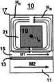
도 5에서, 자기 메모리 셀(10)은, 변경 가능한 자화 배향으로서 데이터 비트를 기억하는 강자성체 데이터층(11)(자기 메모리 셀 분야에서, 강자성체 데이터층(11)은 기억층 혹은 비트층으로 불리워지기도 함)과, 강자성체 데이터층(11)과 전기적으로 통신하는 제 1 도전체(29)와, 강자성체 데이터층(11)과 접촉하는 중간층(13)과, 중간층(13)과 접촉하는 강자성체 캡층(15)과, 강자성체 캡층(15)과 접촉하며 비-핀 고정 자화 배향을 가지며 판독 기입 도전체(19)와 이 판독 기입 도전체(19)를 완전히 둘러싸서 클래드형 판독 기입 도전체를 형성(즉, 판독 기입 도전체(19)는 강자성체 클래딩(21)에 의해 모든 측면들이 전부 둘러싸임)하는 강자성체 클래딩(21)을 포함하는 연성 강자성체 기준층(17)을 포함한다. 연성 강자성체 기준층(17)은 점선(16)으로 도시된 바와 같이 강자성체 클래딩(21)의 일부를 따라 강자성체 캡층(15)과 접촉한다(이후부터 강자성체 클래딩(21)은 클래딩(21)으로, 강자성체 캡층(15)은 캡층(15)으로 불리워질 것이다). 클래딩(21)과 캡층(15)이 도 5에 도시된 바와 같이 서로 같은 높이의 에지를 가질 필요는 없다. 예를 들면, 한 쪽의 에지가 다른 쪽의 에지에 오버랩되거나 삽입될 수도 있다.In Fig. 5, the
더 나아가, 클래딩(21)은, 캡층(15)과 접촉하는 클래딩(21)의 부분을 따라서는 박막 부분을 갖고 캡층(15)과 접촉하지 않는 클래딩(21)의 다른 부분을 따라서는 후막 부분을 갖는 절단된 두께를 갖는다. 부가적으로, 연성 강자성체 기준층(17)의 자화 배향은 핀 고정되지 않는데, 즉, 연성 강자성체 기준층(17)이 예컨대 자장에서의 어닐링같은 종래의 처리를 이용한 자기 메모리 셀(10)의 제조 동안에 설정된 사전 정의된 자화 배향을 갖지 않는다.Furthermore, the
대신에, 도 6에서, 사전 정의된 크기의 외부 공급된 판독 전류 IR가 판독 기입 도전체(19)를 통해 흐르고, 그 결과 판독 자장 HR이 발생된다. 도 6에서, 판독 전류 IR는 "+" 부호로 표시된 바와 같이 페이지 속으로 흐르고 있고, 결국 판독 자장 HR은 오른손 법칙에 따라 시계방향으로 벡터를 갖는다. 판독 자장 HR은 실질적으로 클래딩(21) 내에 포함된다. 판독 자장 HR의 결과로서, 연성 강자성체 기준층(17)은 동적으로 핀 고정(즉, 즉석에서 핀 고정)되는 자화 배향 M1을 갖고, M1은 좌측을 지시하고 있다. 전류 IR가 계속해서 판독 기입 도전체(19)로 흐르는 한, 자화 배향 M1은 계속해서 동적으로 핀 고정된다. 판독 전류 IR가 흐르는 동안, 중간층(13)을 통해 강자성체 데이터층(11)과 연성 강자성체 기준층(17) 사이를 흐르는 전자로 인해 강자성체 데이터층(11)과 연성 강자성체 기준층(17) 사이에는 저항이 존재한다. 강자성체 데이터층(11)에 기억된 데이터 비트의 상태는 그 저항의 크기 및/또는 변화를 측정함으로써 결정될 수 있다. 예를 들어, 저항은 연성 강자성체 기준층(17)과 제 1 도전체 사이에서 측정될 수 있다.Instead, in FIG. 6, an externally supplied read current IR of a predefined magnitude flows through the
도 6에서, 자기 메모리 셀(10)은 캡층(15)을 포함하지 않는다(도 5 참조). 그러나, 도 8a 내지 도 9b를 참조하여 이후에 설명되는 바와 같이, 본 발명의 연성 강자성체 기준층(17)을 참조하여 도 6에서 전술된 원리는 자기 메모리 셀(10)이 캡층(15)을 포함하는 여부와 무관하게 적용된다. 캡층(15)은 선택 사양이다. 캡층(15)이 제공되면(도 8a 내지 도 9b 참조), 판독 자장 HR은 실질적으로 클래딩(21)과 캡층(15) 내에 실질적으로 포함되는데, 그 이유는 클래딩(21)과 캡층(15)은 둘 다 강자성체 물질로 만들어지고, 서로 접촉할 때 자기적으로 하나가 되기 때문이다.In FIG. 6, the
저항을 유발하는 현상은 자기 메모리에서 공지된 것이고, TMR, GMR 및 CMR 메모리 셀에 대해서도 공지된 것이다. 예를 들어, TMR 기반형 메모리 셀에서, 이런 현상은 양자 역학적 터널링 혹은 스핀-의존 터널링으로 불리운다. TMR 메모리 셀에서, 중간층(13)은 절연 물질로 된 박막의 터널 장벽층인데, 이것을 통해 전자 양자가 강자성체 데이터층(11)과 연성 강자성체 기준층(17) 사이를 기계적으로 관통(즉, 이동)한다. 한편, GMR 기반형 메모리 셀에서, 이 현상은 전자의 스핀 의존 산란이고, 중간층(13)은 비자기 물질의 박막 스페이서 층이다. 어느 경우든, 강자성체 데이터층(11)과 연성 강자성체 기준층(17) 사이의 저항은 M1과 M2의 상대적인 배향에 따라 변하고, 이러한 저항 변화는 강자성체 데이터층(11)에 기억된 데이터 비트가 논리 "0"인지 혹은 논리 "1"인지 결정하기 위해 감지될 수 있다.The phenomenon causing resistance is known in magnetic memory and also known in TMR, GMR and CMR memory cells. For example, in TMR based memory cells, this phenomenon is called quantum mechanical tunneling or spin-dependent tunneling. In a TMR memory cell, the
따라서, 강자성체 데이터층(11)에 기억된 데이터 비트는, 전술한 바와 같이 판독 기입 도전체(19)을 통해 판독 전류 IR를 통과시킨 뒤에 강자성체 데이터층(11)과 연성 강자성체 기준층(17) 사이의 저항을 측정함으로써 자기 메모리 셀(10)에 대한 판독 동작 동안에 판독될 수 있다. 비트의 논리 상태(즉, 논리 "0" 혹은 논리 "1")는 저항의 크기를 감지하여 결정될 수 있다. M1과 M2의 상대적 배향으로부터 비트의 논리 상태가 결정되는 방법의 일 예가 도 8a, 도 8b, 도 9a, 도 9b를 참조하여 이제부터 설명될 것이다.Accordingly, the data bits stored in the
도 8a에서, 판독 전류 IR이 "+" 부호로 표시된 바와 같이 페이지 속으로 흐르면, 판독 자장 HR은 시계 방향의 벡터를 가지며, 연성 강자성체 기준층(17)의 즉석 핀 고정된 자화 배향 M1은 강자성체 데이터층(11)의 변경 가능한 자화 배향 M2와 평행한데, 즉, M1과 M2가 동일 방향을 지시한다. 이러한 M1과 M2의 배열은 논리 "0"을 나타내도록 사전 정의된 강자성체 데이터층(11)과 연성 강자성체 기준층(17) 사이의 저항을 초래한다.In FIG. 8A, when the read current IR flows into the page as indicated by the "+" sign, the read magnetic field HR has a clockwise vector, and the instantaneous pinned magnetization orientation M 1 of the soft
한편, 도 8b에서, 강자성체 데이터층(11)의 변경 가능한 자화 배향 M2는 연성 강자성체 기준층(17)의 즉석 핀 고정된 자화 배향 M1와 반평행하고, 즉 M1과 M2가 반대 방향을 지시한다. 따라서, 이러한 M1과 M2의 배열은 논리 "1"을 나타내도록 사전 정의된 강자성체 데이터층(11)과 연성 강자성체 기준층(17) 사이의 저항을 초래한다.On the other hand, in FIG. 8B, the changeable magnetization orientation M2 of the
또 다른 예로서, 도 9a에서, 판독 전류 IR은 "●" 부호로 표시된 바와 같이 페이지 밖으로 흐르고, 연성 강자성체 기준층(17)의 즉석 핀 고정된 자화 배향 M1은 강자성체 데이터층(11)의 변경 가능한 자화 배향 M2와 반평행하다. 또한, 판독 자장 HR은 시계 반대 방향의 벡터를 가지며, M1은 우측을 지시한다. M1과 M2의 이러한 배열은 논리 "1"을 나타내도록 사전 정의된 강자성체 데이터층(11)과 연성 강자성체 기준층(17) 사이의 저항을 초래한다.As another example, in Fig. 9A, the read current IR flows out of the page as indicated by the symbol "" Antiparallel to the magnetization orientation M2. In addition, the read magnetic field HR has a counterclockwise vector and M 1 points to the right. This arrangement of M1 and M2 results in resistance between the
역으로, 도 9b에서, 강자성체 데이터층(11)의 변경 가능한 자화 배향 M2는 연성 강자성체 기준층(17)의 즉석 핀 고정된 자화 배향 M1과 평행하다. 따라서, M1과 M2의 이러한 배열은 논리 "0"을 나타내도록 사전 정의된 강자성체 데이터층(11)과 연성 강자성체 기준층(17) 사이의 저항을 초래한다.Conversely, in FIG. 9B, the changeable magnetization orientation M2 of the
전술한 바와 같이, 도 8a 내지 도 9b에 예시된 판독 동작의 원리는 캡층(15)의 제공 여부와 무관하게 적용된다. 캡층(15)의 포함 혹은 배제는 본 발명의 메모리 셀(10)을 만드는 방법와 연계하여 이후에 설명될 것이다. 더 나아가, 캡층(15)이 제공되면, 이것은 클래딩(21)과 자기적으로 하나이고(즉, 자기적으로 결합됨), 판독 자장 HR은 도 8a 내지 도 9b에 예시된 바와 같이 캡층(15)속으로 뻗어 나간다. 그러므로, 도 8a 내지 도 9b에 예시된 캡층(15)은 선택 사양이다. 캡층(15)은 배제될 수 있으며, 도 8a 내지 도 9b를 참조하여 설명된 판독 동작의 원리는 그대로 적용된다.As mentioned above, the principle of the read operation illustrated in FIGS. 8A-9B applies regardless of whether the
M1과 M2 사이의 평행 및 반평행 관계에 대해 어떤 논리 상태가 배정되었는지를 판정하는 것은 애플리케이션별로 정해질 수 있고, 혹은 이런 결정이 사전 정의된 규약을 통해 행해지는 것도 가능하다. 예를 들어, 도 8a 및 도 8b에 예시된 정렬이 규약으로서 도입될 수 있고, 이로써 판독 전류 IR가 페이지 "+"속으로 흐르면, M1은 원하는 배향(즉, 좌측을 지시함)으로 즉석에서 핀 고정되며, 논리 "0"에 대한 규약은 M1과 M2가 평행한 것이고, 논리 "1"에 대한 규약은 M1과 M2가 반평행한 것이다.Determining which logical state is assigned for the parallel and antiparallel relationships between M1 and M2 may be application specific, or such a decision may be made via a predefined protocol. For example, the alignment illustrated in FIGS. 8A and 8B can be introduced as a protocol such that when read current IR flows into the page "+", M1 is instantaneously in the desired orientation (ie, pointing to the left). Pinned, the convention for logic "0" is parallel to M1 and M2, and the convention for logic "1" is antiparallel to M1 and M2.
본 명세서에 설명된 본 발명의 실시예에서, 강자성체 데이터층(11), 캡층(15), 클래딩(21)은 높은 자기 투자율의 연성 자기 물질로 만들어질 수 있다. "연성 자기 물질"이란 것은, 약 1000 이상의 높은 상대 자기 투자율 μR(즉, 자기 투자율 μ는 μ=μ0* μR이고, 이때 μ0=4π*10-7H/m 이며, μ=(4π*10-7)*1000=1.257*10-3H/m 이상임)과, 약 1000A/m 이하의 보자력(보자성)과, 작은 히스테리시스 손실을 갖는 물질이다.In the embodiments of the present invention described herein, the
클래딩을 위한 높은 자기 투자율의 연성 자기 물질은 자화 배향 M1이 클래딩(21)을 포화시키지 않는 판독 자장 HR의 크기에도 즉석 핀 고정될 수 있게 하는데, 클래딩이 포화되지 않으면 판독 자장 HR은 실질적으로 클래딩(21) 내에 포함된다. 더 나아가, 클래딩(21)의 바깥으로 뻗어 나가는 판독 자장 HR의 어떤 부분(즉, 판독 자장이 클래딩(21)의 내부에 포함되지 않음)은 강자성체 데이터층(11)의 변경 가능한 자화 배향 M2을 회전시키지 않는다(즉, 판독 자장 HR이 M2를 자신의 현재 배향으로부터 전환시키지 않음). 그 결과, 판독 자장 HR을 발생시키는데 필요한 판독 전류 IR의 크기가 종래의 자기 메모리 셀보다 작아진다. 마찬가지로, 연성 강자성체 기준층(17)이 캡층(15)을 포함할 경우에는, 클래딩(21)과 캡층(15) 둘 다를 위한 높은 자기 투자율의 연성 자기 물질은 클래딩(21)과 캡층(15)을 포화시키지 않을 정도의 크기의 판독 자장 HR으로 자화 배향 M1이 즉석 핀 고정되는 것을 허용하는데, 클래딩(21)과 캡층(15)을 포화되지 않으면 판독 자장 HR이 실질적으로 클래딩(21)과 캡층(15) 내에 포함되어, 클래딩(21)과 캡층(15)밖으로 뻗어 나간 판독 자장 H의 어떠한 부분도 강자성체 데이터층(11)의 변경 가능한 자화 배향 M2을 회전시키지 않는다.If the soft magnetic material of high magnetic permeability for the cladding orientation of magnetization M1 is to be able to be fixed to the fly pin size of the read magnetic field HR that does not saturate the
반대로, 클래딩(21)을 위한 높은 자기 투자율의 연성 자기 물질은 제 1 기입 전류 IW1에 의해 발생된 제 1 기입 자장 HW1이 클래딩(21)을 포화시켜 제 1 기입 자장 HW1이 강자성체 데이터층(11)을 향해 클래딩(21)밖으로 뻗어나가는 것을 허용한다. 만약 캡층(15)이 제공되면, 제 1 기입 자장 HW1이 클래딩(21)과 캡층(15)을 모두 포화시키고 강자성체 데이터층(11)밖으로 뻗어나간다. 어떤 경우든, 클래딩의 박막 부분은 기입 동작 동안 클래딩의 포화를 지원하도록 동작하고, 이 때 제 1 기입 전류 IW1의 크기는 포화 자장 즉, 제 1 기입 자장 HW1을 발생시키기에 충분하다.Conversely, a high magnetic permeability soft magnetic material for the
본 발명의 일 실시예에서, 강자성체 데이터층(11), 캡층(15), 클래딩(21)중 하나 이상 선택된 것을 위한 높은 자기 투자율의 연성 자기 물질은 이하의 표 1에 열거된 물질로 만들어질 수 있지만, 반드시 열거된 물질에만 한정되는 것은 아니다.In one embodiment of the invention, the high magnetic permeability soft magnetic material for one or more of the
본 발명의 다른 실시예에서, 강자성체 데이터층(11), 캡층(15), 클래딩(21)은 동일한 높은 자기 투자율의 연성 자기 물질로 만들어질 수 있다. 동일한 높은 자기 투자율의 연성 자기 물질은 전술한 표 1에 설정된 물질들을 포함하지만, 반드시 이것에만 한정되지는 않는다. 예를 들어, NiFe 혹은 퍼멀로이가 강자성체 데이터층(11), 캡층(15), 클래딩(21)을 만드는데 이용될 수 있다.In another embodiment of the present invention, the
본 발명의 일 실시예에서, 강자성체 데이터층(11), 캡층(15), 클래딩(21)중 하나 이상 선택된 것은 약 1000을 초과하는 상대 자기 투자율을 갖는다.In one embodiment of the present invention, one or more selected of the
본 발명의 다른 실시예에서, 강자성체 데이터층(11), 캡층(15), 클래딩(21)중 하나 이상 선택된 것은 약 1000A/m 이하인 보자성을 갖는다.In another embodiment of the present invention, at least one of the
판독 기입 도전체(19)는 전기적으로 도전성인 물질로 제조되는다. 판독 기입 도전체(19)로 적합한 물질은 표 2에 열거되었지만, 반드시 이것에만 한정되는 것은 아니다.The
본 발명의 일 실시예에서, 중간층(13)은 연성 강자성체 기준층(17)으로부터 강자성체 데이터층(11)을 분리하여 전기적으로 절연시키는 절연 물질로 제조되는 터널 장벽층이다(즉, 이것은 전기적으로 도전성이 아니다). 반드시 한정되는 것은 아니지만 이후의 표 3에 열거된 절연 물질들이 터널 장벽층용으로 이용될 수 있다. 터널 장벽층은 약 0.5nm 내지 5.0nm인 두께를 가질 수 있다.In one embodiment of the invention, the
본 발명의 다른 실시예에서, 중간층(13)은 비자기 물질로 잔들어진 스페이서 층(spacer layer)이다. 스페이서 층용 비자기 물질은 3d, 4d 혹은 5d 천이 금속(원소 주기율표로부터)일 수 있다. 반드시 한정되는 것은 아니만 이하의 표 4에 열거된 비자기 물질은 스페이서 층용으로 이용 가능하다. 스페이서 층은 약 0.5nm 내지 5.0nm의 두께를 가질 수 있다.In another embodiment of the present invention, the
도 11에서, 본 발명의 자기 메모리 셀(10)은 강자성체 데이터층(11)을 가로질러 강자성체 데이터층(11)과 전기적으로 통신하고 있는 제 1 도전체(29)를 포함할 수 있다. 강자성체 데이터층(11)과 제 1 도전체(29) 사이의 전기적 통신은 제 1 도전체(29)와 강자성체 데이터층(11)이 서로 접촉하거나 혹은 도전성 플러그 등(도시 안됨)을 통한 상호 접속 구조에 의해 수행 가능하다. 바람직하게는, 제 1 도전체(29)가 강자성 데이터층(11)과 접촉하는 것인데, 그 이유는 이런 배열이 콤팩트하고 상호 접속 구조보다 덜 복잡하기 때문이다. 데이터 비트는 제 1 도전체(29)와 연성 강자성체 기준층(17) 사이의 저항을 측정함으로써 전술한 바와 같이 판독될 수 있다. 제 1 도전체(29)는 실질적으로 직교 방향으로 강자성체 데이터층(11)을 가로지를 수 있으며, 혹은 제 1 도전체(29)가 비직교 방향으로 강자성체 데이터층(11)을 가로지를 수도 있다. 전형적으로, 제 1 도전체(29)는 직교 방향으로 강자성체 데이터층(11)을 가로지르는데, 그 이유는 마이크로일렉트로닉 레이아웃과 라우팅 툴이 마이크로일렉트로닉 장치의 직교 레이아웃에 대해 보정가능하고, 일부 툴은 비직교 레이아웃을 허용하지 않기 때문이다. 제 1 도전체(29)는 반드시 한정되는 것은 아니지만 전술한 표 2에 설정된 전기 도전 물질로 형성될 수 있다.In FIG. 11, the
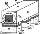
도 7에서, 메모리(50)는 본 발명의 다수의 자기 메모리 셀(10)로 형성된다. 각 자기 메모리 셀(10)은 공통 연성 강자성체 기준층(17)과 접촉하는 각각의 캡층(15)(캡층(15)은 선택 사양임)을 가지며, 각각의 자기 메모리 셀(10)은 각각의 강자성체 데이터층(11)에 데이터 비트를 기억한다. 데이터 비트는 강자성체 데이터층(11)과 연성 강자성체 기준층(17) 사이의 저항을 측정함으로써 판독될 수 있다. 또한, 도 11을 참조하여 전술한 바와 같이, 각각의 자기 메모리 셀(10)은 각각의 강자성체 데이터층(11)과 전기적으로 통신하는 제 1 도전체(29)를 포함한다. 마찬가지로, 데이터 비트는 제 1 도전체(29)와 연성 강자성체 기준층(17) 사이의 저항을 측정함으로써 판독될 수 있다. 따라서, 연성 강자성체 기준층(17)과 제 1 도전체(29)는 각기 열 도전체와 행 도전체와 같이, 혹은 각기 행 도전체와 열 도전체와 같이 한 쌍의 도전체일 수 있다. 한 쌍의 도전체는 서로 교차하고, 자기 메모리 셀(10)은 도 7에 예시된 바와 같이 이 도전체 쌍들 사이의 교차 영역에 위치될 수 있다. 도전체 쌍이 직교 방향으로 서로 교차될 필요는 없다.In Fig. 7, the
종래 기술에서 공지된 바와 같이, 데이터 비트가 강자성체 데이터층(11)에 기입되는 기입 동작은, 제 1 기입 자장 HW1을 발생시키도록 판독 기입 도전체(19)를 통해 제 1 외부 공급 전류 IW1을 통과시키고 제 2 기입 자장 HW2을 발생시키도록 제 1 도전체(29)를 통해 제 2 외부 공급 전류 IW2을 통과시킴으로써 수행될 수 있다. 제 1 및 제 2 기입 자장(HW1, HW2)은 변경 가능한 자화 배향 M2를 원하는 방향으로 회전시키기 위해 강자성체 데이터층(11)과 협력적으로 상호 작용한다. 예를 들어, 만약 M2가 "좌측"을 지시하여 강자성체 데이터층(11)이 현재 논리 "0"을 기억하고 있다면, 제 1 및 제 2 기입 자장(HW1, HW2)은 강자성체 데이터층(11)과 협력적으로 작용하여, M2가 "우측"을 지시하도록 회전시켜서(움직여서), 논리 "1"이 강자성체 데이터층(11)에 기입되게 한다.As is known in the art, a write operation in which data bits are written to the
도 12에서, 메모리(70)는 본 발명의 다수의 자기 메모리 셀(10)에 의해 형성된다. 각각의 자기 메모리 셀(10)은 공통 연성 강자성체 기준층(17)과 접촉하는 각각의 캡층(15)(캡층(15)은 선택 사양임)을 구비하고, 각각의 강자성체 데이터층(11)은 강자성체 데이터층(11)을 가로지르는 제 1 도전체(29)와 전기적으로 통신한다.In FIG. 12,
자기 메모리 셀(10)중 선택된 하나에 대한 기입 동작은 다음과 같이 행해진다. 판독 기입 도전체(19)를 통해 제 1 기입 전류 IW1을 통과시키고 제 1 도전체(29)을 통해 제 2 기입 전류 IW1를 통과시킴으로써, 도면부호(11a)로 표시된 강자성체 데이터층을 갖는 자기 메모리 셀(10)이 기입 동작을 위해 선택된다. 다른 자기 메모리 셀(10)은 기입 동작에 선택되지 않는데, 그 이유는 그들 각각의 제 1 도전체(29)에는 어떠한 전류도 흐르지 않기 때문이다. 제 1 기입 전류 IW1은 제 1 기입 자장 HW1을 발생하고, 제 2 기입 전류 IW2는 제 2 기입 자장 HW1을 발생한다. 제 1 및 제 2 기입 자장(HW1, HW2)은 강자성체 데이터층(11a)의 변경 가능한 자화배향 M2를 원하는 방향으로 회전시키기 위해 협력적으로 작용한다.The write operation for the selected one of the
또 다른 예로서, 동일한 강자성체 데이터층(11a)에 대한 판독 동작은 연성 강자성체 기준층(17)의 판독 기입 도전체(19)를 통해 사전 정의된 크기와 방향의 판독 전류 IR을 통과시킴으로써 달성될 수 있다. 판독 전류 IR은 실질적으로 클래딩(21) 내에 포함되는 판독 자장 HR을 발생하고, 판독 자장 HR은 자화 배향 M1을 즉석 핀 고정하도록 동작한다. 강자성체 데이터층(11)에 기억된 데이터 비트는 연성 강자성체 기준층(17)과 강자성체 데이터층(11a)의 제 1 도전체(29) 사이의 저항을 측정함으로써 판독될 수 있다(도 7 참조).As another example, a read operation on the same
도 14a 및 도 14b에서, 기입 동작이 더 상세히 예시된다. 도 14a에서, 변경 가능한 자화 배향 M2는 기입 동작의 시점에서 좌측을 지시하고 있다. 제 1 및 제 2 기입 자장(HW1, HW2)은 강자성체 데이터층(11)을 향해 뻗어 있고, 서로 작용하면, 제 1 및 제 2 기입 자장(HW1, HW2)이 M2를 회전시키기 시작한다. 제 1 기입 전류 IW1의 크기(점선으로 표시)는 제 1 기입 자장 HW1이 클래딩(21)과 (박막 부분을 따른) 캡층(15)을 포화시켜서 제 1 기입 자장 HW1이 강자성체 데이터층(11)속으로 뻗어 나갈 정도이다. 다음에, 도 14b에서, 제 1 및 제 2 기입 자장(HW1, HW2)의 조합된 자력이 M2에 대해 작용한 결과로서, 변경 가능한 자화 배향 M2가 회전되어 우측을 지시한다. 만약 M2가 좌측을 지시할 때 논리 "0"을 나타낸다면, 우측을 지시하는 M2는 논리 "1"을 표시한다.In Figures 14A and 14B, the write operation is illustrated in more detail. In Fig. 14A, the changeable magnetization orientation M2 points to the left at the time of the write operation. The first and second write magnetic fields HW1 , HW2 extend toward the
본 발명의 클래드형 판독 기입 도전체를 만드는 프로세스는 도 10a 내지 도 10f에 예시된다. 이하에 설정되는 프로세스 단계들의 순서는 단지 예시를 위한 것으로, 실제 프로세스 단계 순서가 이하에 설정된 것과 동일한 순서일 필요는 없다. 더 나아가, 마이크로일레트로닉 기술 분야의 기술자에게 공지된 다른 프로세스들이 본 명세서에 설정된 프로세스를 대신할 수도 있다.The process of making the clad read write conductor of the present invention is illustrated in FIGS. 10A-10F. The order of process steps set forth below is for illustrative purposes only, and the actual process step order need not be the same as set below. Furthermore, other processes known to those skilled in the microelectronics art may replace the processes set forth herein.
먼저, 도 10a에서, 절연층(31)이 형성되고, 이것은 예컨대 CMP같은 프로세스에 의해 평탄화된다. 클래딩(21)의 일부를 형성하게 될 높은 자기 투자율의 연성 자기 물질을 증착하기 전에 트렌치(33)가 절연층(31)내에 에치된다. 비록 절연층(31)의 일부만이 도 10a에 예시되었지만, 절연층(31)은 그 속에 형성되는 다수의 트렌치(33)를 갖는 절연층일 수 있고, 점선 e로 도시된 바와 같이 확장될 수 있다.First, in Fig. 10A, an insulating
두 번째, 도 10b에서, 클래딩(21a)의 일부가 등방성 프로세스를 이용해 트렌치(33)에 증착된다(그러므로 트렌치(33)의 측벽이 트렌치(33)의 바닥 b와 거의 동일한 두께로 입혀진다). 클래딩(21a)에 이용되는 물질은 자기적으로 연성인 물질, 즉, 자기 코어로 작용하기에 충분할 정도로 투과성이고, 어떠한 틈(breaks)이나 너무 많은 보이드(voids)없이 단면적 전반에 걸쳐 연속적이다. 트렌치(35)는 클래딩(21a)의 등방성 증착의 결과로 형성된다.Second, in FIG. 10B, a portion of the
세 번째, 도 10c에서, 트렌치(35)는 판독 기입 도전체(19)를 형성하는 전기도금이나 적절한 증착 프로세스를 이용해 구리(cu)같은 전기 도전성 물질로 채워진다. 다음에, 전체 구조는 (예컨대 CMP를 이용하여) 평탄화되어, 도 10c에 예시된 구조를 만든다. 도 10c에서 판독 기입 도전체(19)는 아직 완전히 클래드되지 않았음을 유의하자.Third, in FIG. 10C,
네 번째, 도 10d에서, 다른 높은 자기 투자율의 연성 자기 물질(21b)이 자속 경로에 근접하여 증착되어, 전체가 클래드된 판독 기입 도전체(19)를 형성한다(즉, 이것은 클래딩 세그먼트(21a) 및 (21b)에 의해 완전히 둘러싸임). 높은 자기 투자율의 연성 자기 물질(21b)의 두께는 클래딩(21a)의 측벽 S 혹은 바닥 b의 두께와 다르게 만들어질 수 있다. 세그먼트(21b)용 물질은 클래딩(21a)용 물질과 같거나 다를 수 있다. 그 다음에, 클래딩(21b)이 패턴화 및 에치되고, 자기 메모리 셀(10)의 나머지 부분이 도 10d의 구조의 상부에 형성된다. 또한, 비록 도 10d는 클래딩(21a)의 최외곽 에지를 넘어 뻗어 있는 높은 자기 투자율의 연성 자기 물질(21b)을 예시했더라도, 높은 자기 투자율의 연성 자기 물질(21b)은 이들 에지를 넘어서거나 혹은 점선 i로 도시된 바와 같이 에지로부터 삽입될 수 있다. 높은 자기 투자율의 연성 자기 물질(21b)이 클래딩(21a)과 폐쇄된 자속 경로를 형성하지 못할 정도로 삽입(i)되어서는 안된다.Fourth, in FIG. 10D, another high magnetic permeability, soft
선택 사양으로서, 도 10e에서, 캡층(15)을 형성하기 위해 다른 높은 자기 투자율의 연성 자기 물질이 클래딩(21a)상에 증착될 수도 있다(이전에는 도면부호(21a)와 (21b)로 표시됨). 그 다음에, 중간층(13)이 캡층(15)상에 증착된다. 캡층(15)의 포함은 제조상 선택 문제이다. 예를 들어, 전술한 바와 같이, 프로세스 단계들은 본 명세서에 기술된 순서를 따를 필요가 없다. 이를 위해, 자기 메모리 셀(10)은 강자성 데이터층(11)으로 개시하여, 그 후 중간층(13) 등이 형성되는 것에 의해 제조될 수도 있다. 중간층(13)에 이용되는 물질에 따라서, 증착된 이후의 노출 환경과 화학적으로 반응하는 것을 막기 위해 중간층(13)을 완료(즉, 패시베이트)하는 것이 필요할 수도 있다. 예를 들어, 만약 중간층(13)이 절연 터널 장벽층이라면, 클래딩(21)의 높은 자기 투자율의 연성 자기 물질과 자기적으로 양립하게 될 높은 자기 투자율의 연성 자기 물질로 제조되는 캡층(15)을 증착하는 것이 바람직할 수도 있다. 캡층(15)은 절연 터널 장벽층에 대해 보호 캡의 역할을 한다. 캡층(15)은 클래딩(21)과 동일하거나 다른 물질로 만들어 질 수 있다.Optionally, in FIG. 10E, other high magnetic permeability soft magnetic materials may be deposited on
마지막으로, 도 10f에서, 강자성체 데이터층(11)이 중간층(13)상에 형성된다. 또한, 전기 도전성 물질이 강자성체 데이터층(11)상에 증착되어 제 1 도전체(29)를 형성할 수 있다.Finally, in FIG. 10F, a
전술한 프로세스는 본 발명의 완전 클래드된 판독 기입 도전체(즉, 도면부호(19), (21a)및 (21b))를 형성하는데 이용되는 Cu-상감기법 프로세스(Cu-damascene process)의 것을 흉내낸다. 이러한 프로세스가 만들어내는 평면 구조는 도 10d의 구조를 제조하는데 유리하다(그러나 절대적으로 필수적인 것은 아니다). 그러나, 마이크로일렉트로닉스 분야에서 알려진 다른 프로세스들이 도 10d의 구조를 제조하는데 이용되는 것도 가능하다. 또한, 도 10a 내지 도 10f는 본 발명의 전체 클래드된 판독 기입 도전체를 제조하는 한 가지 가능한 방법을 예시하는 것이다. 예를 들어, 도 10a 내지 도 10f에 예시된 것의 역순으로 제조하는 것도 가능하다. 제조는 강자성체 데이터층(11)으로 시작하여 중간층(13)과 선택 사양인 캡층(15)으로 진행한 뒤, 클래드된 판독 기입 도전체의 형성으로 진행할 수도 있다.The foregoing process mimics that of the Cu-damascene process used to form the fully clad read write conductors of the present invention (ie,
전술한 프로세스에서, 클래딩(21)과 캡층(15)과 강자성체 데이터층(11)과 판독 기입 도전체(19)와 중간층(13)용으로 이용되는 물질들은 반드시 그런 것은 아니지만 전술한 표 1, 표 2, 표 3, 표 4에 예시된 것들을 포함한다.In the above process, the materials used for the
도 13a에서, 클래딩(21), 중간층(13), 강자성체 데이터층(11) 사이의 디멘젼 관계가 예시된다. 전술한 바와 같이, 클래딩(21)용의 연성 자기 물질이 선택되면, 판독 기입 도전체(19)에 흐르는 판독 전류 IR에 의해 발생된 판독 자장 HR이 연성 강자성체 기준층(17)의 자화 배향 M1을 즉석 핀 고정할 것이다. 또한, 이렇게 발생된 판독 자장 HR은 클래딩(21)을 포화시키지 않아서, 판독 동작 동안에 판독 자장 HR은 실질적으로 클래딩(21) 내에 포함된다. 클래딩(21)을 초과하지 않는 판독 자장 H의 어떤 부분은 강자성체 데이터층(11)의 변경 가능한 자화 배향 M2를 회전시키지 않는다. 이와 대조적으로, 기입 동작 동안에는, 제 1 기입 자장 HW1이 클래딩(21)을 포화시켜서, 강자성 데이터층(11)을 행해 뻗어나간다. 결국, 클래딩(21)의 상대적인 두께는, 판독 동작 동안에는 판독 자장 HR이 클래딩 내에 실질적으로 포함되고 기입 동작 동안에는 제 1 기입 자장 HW1이 클래딩(21)을 포화시키도록 절단되어야 한다.In FIG. 13A, the dimension relationship between the
도 13a에서, 중간층(13)에 인접한 클래딩(21)의 부분(즉, 점선(18)으로 표시된 것같은 박막 부분)은 판독 자장 HR을 클래딩(21) 내에 실질적으로 포함하기에 충분한 최소 두께 D1을 가져야 한다(즉, 자속 폐쇄를 제공할 정도로 두꺼움). 클래딩(21)의 나머지 부분은 최소 두께 D1 이상인 두께 D2, D3 및 D4를 가질 수 있고, 그러므로 D2, D3 및 D4≥ D1 이다. 바람직하게는, D2, D3 및 D4가 D1보다 더 큰 두께를 갖는다.In FIG. 13A, the portion of the
기입 동작 동안, 제 1 기입 자장 HW1은 클래딩(21)을 포화시키는데, 그러나 D2, D3 및 D4가 실질적으로 D1보다 더 두껍게 클래딩(21)의 두께를 절단하여, 제 1 기입 자장 HW1이 실질적으로 강자성체 데이터층(11)을 향하는 방향으로 박막 부분을 따라 클래딩(21)을 포화시키도록 하는 것이 바람직할 수도 있다. 그 결과, 제 1 기입 자장 HW1은 강지성체 데이터층(11)을 향하는 방향으로 관통하고, 두께 D2, D3 및 D4의 방향(즉, 후막 부분)으로의 주변 기생 자장은 클래딩(21)을 포화시키지 않거나 혹은 D2, D3 및 D4에서클래딩(21)의 두께에 의해 실질적으로 최소로 감쇠된다. 바람직하게는, D2, D3 및 D4가 클래딩(21)의 포화를 막도록 선택된 두께를 갖는다.During a write operation, the first write magnetic field HW1 saturates the
마찬가지로, 도 13b에 클래딩(21), 캡층(15), 중간층(13), 강자성체 데이터층(11) 사이의 디멘젼 관계가 예시된다. 전술한 바와 같이, 클래딩(21)과 캡층(15)용의 연성 자기물질이 선택되면, 판독 기입 도전체(19)에 흐르는 판독 전류 IR에 의해 발생된 판독 자장 HR이 연성 강자성체 기준층(17)의 자화 배향 M1을 즉석 핀 고정할 것이다. 또한, 이렇게 발생된 판독 자장 HR은 클래딩(21)과 캡층(15)을 포화시키지 않아서, 판독 자장 HR이 실질적으로 클래딩(21)과 캡층(15) 내에 포함된다(즉, 클래딩(21)과 캡층(15)이 자속 폐쇄를 제공한다). 클래딩(21)과 캡층(15)을 초과하지 않는 판독 자장 Hr의 어떤 부분은 강자성체 데이터층(11)의 변경 가능한 자화 배향 M2를 회전시키지 않는다. 반대로, 기입 동작 동안에는, 제 1 기입 자장 HW1이 클래딩(21)과 캡층(15)을 포화시켜서, 강자성 데이터층(11)을 행해 뻗어나간다. 그러므로, 클래딩(21)의 상대적인 두께는, 판독 동작 동안에는 판독 자장 HR이 클래딩과 캡층내에 실질적으로 포함되고 기입 동작 동안에는 제 1 기입 자장 HW1이 클래딩(21)과 캡층(15)을 포화시키도록 절단되어야 한다.Similarly, the dimension relationship between the
도 13b에서, 캡층(15)에 인접한 클래딩(21)의 부분(즉, 점선(19)으로 표시)은 판독 자장 H을 클래딩(21)과 캡층(15) 내에 실질적으로 포함하기에 충분한 최소 조합 두께 (D1+T1)를 가져야 한다. 클래딩(21)의 나머지 부분은 최소 조합 두께 (D1+T1) 이상인 두께 D2, D3 및 D4를 가질 수 있고, 그러므로 D2, D3 및 D4≥ (D1+T1) 이다. 바람직하게는, D2, D3 및 D4가 (D1+T1)보다 더 큰 두께를 갖는다. 전술한 바와 같이, D2, D3 및 D4는 (D1+T1)보다 실질적으로 더 두껍게 만들어져서, 기입 동작 동안에 제 1 기입 자장 HW1은 실질적으로 강자성체 데이터층(11)을 향하는 방향으로 클래딩(21)과 캡층(15)을 포화시킨다.In FIG. 13B, the portion of the
클래딩(21), 캡층(15), 중간층(13), 강자성체 데이터층(11)에 대한 두께와 두께 범위는 이하에 설정되지만, 반드시 이것에 한정되는 것은 아니다.Although the thickness and thickness range with respect to the
클래딩(21)은 약 3.0nm 내지 약 100.0nm의 두께 D1를 가질 수 있고, 캡층(15)은 약 1.0nm를 넘는 두께 T1를 가질 수 있다. D1과 T1의 실제 두께는 클래딩(21)과 캡층(15)으로 선택된 물질에 따라 좌우될 것이다.The
중간층(13)은 약 0.5nm 내지 약 5.0nm인 두께 T3를 가질 수 있다. T3의 실제 두께는 중간층(13)으로 선택된 물질과, 예컨대 TMR 메모리 셀 혹은 GMR 메모리 셀같은 메모리 셀의 유형에 부분적으로 좌우될 것이다.The
강자성 데이터층(11)은 약 1.0nm를 넘는 두께 T5를 가질 수 있다. T5의 실제 두께는 메모리셀의 유형과 그 애플리케이션에 따라 좌우될 것이다.The
연성 강자성체 기준층(17)은 판독 기입 도전체(19)에 선택된 디멘젼과 클래딩(21)의 두께 D1, D2, D3, D4에 부분적으로 의존하는 높이 H와 폭 W을 가질 수 있다. 그러므로, 최종 디멘젼은 클래딩(21)과 판독 기입 도전체(19)의 디멘젼을 포함한 많은 변수들에 의거하므로, W와 H는 강한 애플리케이션 의존성을 나타낼 것이다.The soft
비록 본 발명의 몇몇 실시예가 개시 및 예시되었지만, 본 발명이 설명 및 예시된 것과 같은 부분들의 특정 형태나 배열에 한정되지는 않는다. 본 발명은 오로지 특허청구범위에 의해서만 한정된다.
Although some embodiments of the invention have been disclosed and illustrated, the invention is not limited to the specific form or arrangement of parts as described and illustrated. The invention is limited only by the claims.
따라서, 본 발명에 따르면, 연성 강자성체 기준층(17)의 자화 배향 M1이 메모리 셀에 대한 판독 동작 동안에 원하는 방향으로 동적으로 즉석 핀 고정된다.Thus, according to the present invention, the magnetization orientation M1 of the soft
또한, 본 발명에 따르면, 연성 강자성체 기준층의 강자성체 클래딩(21)은 실질적으로 인접 자기 메모리 셀(10)에 기억된 데이터를 손상시킬 수 있는 주변 기생 자장을 감소시키고, 연성 강자성체 기준층(17)은 종래의 기핀 고정 기준층을 형성하는데 필요한 층의 수와 복잡성을 줄여 주며, 데이터 비트를 판독 또는 기입하기에 충분한 판독 전류 IR의 크기도 연성 강자성체 기준층(17)에 의해 감소된다.Further, according to the present invention, the
Claims (11)
Translated fromKoreanApplications Claiming Priority (2)
| Application Number | Priority Date | Filing Date | Title |
|---|---|---|---|
| US09/825,461US6404674B1 (en) | 2001-04-02 | 2001-04-02 | Cladded read-write conductor for a pinned-on-the-fly soft reference layer |
| US09/825,461 | 2001-04-02 |
Publications (2)
| Publication Number | Publication Date |
|---|---|
| KR20030009094A KR20030009094A (en) | 2003-01-29 |
| KR100816746B1true KR100816746B1 (en) | 2008-03-26 |
Family
ID=25244051
Family Applications (1)
| Application Number | Title | Priority Date | Filing Date |
|---|---|---|---|
| KR1020020017756AExpired - Fee RelatedKR100816746B1 (en) | 2001-04-02 | 2002-04-01 | Cladded read-write conductor for a pinned-on-the-fly soft reference layer |
Country Status (6)
| Country | Link |
|---|---|
| US (1) | US6404674B1 (en) |
| EP (1) | EP1248265A3 (en) |
| JP (1) | JP3942931B2 (en) |
| KR (1) | KR100816746B1 (en) |
| CN (1) | CN1329916C (en) |
| TW (1) | TW541530B (en) |
Cited By (1)
| Publication number | Priority date | Publication date | Assignee | Title |
|---|---|---|---|---|
| KR101001742B1 (en)* | 2003-10-24 | 2010-12-15 | 삼성전자주식회사 | Magnetic RAM and Manufacturing Method |
Families Citing this family (67)
| Publication number | Priority date | Publication date | Assignee | Title |
|---|---|---|---|---|
| US6351409B1 (en)* | 2001-01-04 | 2002-02-26 | Motorola, Inc. | MRAM write apparatus and method |
| US6504221B1 (en)* | 2001-09-25 | 2003-01-07 | Hewlett-Packard Company | Magneto-resistive device including soft reference layer having embedded conductors |
| US6538917B1 (en)* | 2001-09-25 | 2003-03-25 | Hewlett-Packard Development Company, L.P. | Read methods for magneto-resistive device having soft reference layer |
| US6936903B2 (en)* | 2001-09-25 | 2005-08-30 | Hewlett-Packard Development Company, L.P. | Magnetic memory cell having a soft reference layer |
| US6545906B1 (en) | 2001-10-16 | 2003-04-08 | Motorola, Inc. | Method of writing to scalable magnetoresistance random access memory element |
| US6549447B1 (en)* | 2001-10-31 | 2003-04-15 | Peter Fricke | Memory cell structure |
| DE10158795B4 (en)* | 2001-11-30 | 2005-12-22 | Infineon Technologies Ag | Magnetoresistive memory cell with dynamic reference layer |
| US6661688B2 (en)* | 2001-12-05 | 2003-12-09 | Hewlett-Packard Development Company, L.P. | Method and article for concentrating fields at sense layers |
| US6552554B1 (en)* | 2001-12-06 | 2003-04-22 | The United States Of America As Represented By The Secretary Of The Navy | Testing current perpendicular to plane giant magnetoresistance multilayer devices |
| US6750491B2 (en)* | 2001-12-20 | 2004-06-15 | Hewlett-Packard Development Company, L.P. | Magnetic memory device having soft reference layer |
| US6593608B1 (en)* | 2002-03-15 | 2003-07-15 | Hewlett-Packard Development Company, L.P. | Magneto resistive storage device having double tunnel junction |
| US6728132B2 (en)* | 2002-04-03 | 2004-04-27 | Micron Technology, Inc. | Synthetic-ferrimagnet sense-layer for high density MRAM applications |
| US6780653B2 (en) | 2002-06-06 | 2004-08-24 | Micron Technology, Inc. | Methods of forming magnetoresistive memory device assemblies |
| US6707087B2 (en) | 2002-06-21 | 2004-03-16 | Hewlett-Packard Development Company, L.P. | Structure of chalcogenide memory element |
| US6683815B1 (en)* | 2002-06-26 | 2004-01-27 | Silicon Magnetic Systems | Magnetic memory cell and method for assigning tunable writing currents |
| US6744663B2 (en)* | 2002-06-28 | 2004-06-01 | Motorola, Inc. | Circuit and method for reading a toggle memory cell |
| US7095646B2 (en) | 2002-07-17 | 2006-08-22 | Freescale Semiconductor, Inc. | Multi-state magnetoresistance random access cell with improved memory storage density |
| US6885576B2 (en)* | 2002-08-13 | 2005-04-26 | Micron Technology, Inc. | Closed flux magnetic memory |
| US6924539B2 (en)* | 2002-08-30 | 2005-08-02 | Hewlett-Packard Development Company, L.P. | Magnetic memory cell having an annular data layer and a soft reference layer |
| US6577529B1 (en)* | 2002-09-03 | 2003-06-10 | Hewlett-Packard Development Company, L.P. | Multi-bit magnetic memory device |
| US6801451B2 (en)* | 2002-09-03 | 2004-10-05 | Hewlett-Packard Development Company, L.P. | Magnetic memory devices having multiple bits per memory cell |
| JP3788964B2 (en)* | 2002-09-10 | 2006-06-21 | 株式会社東芝 | Magnetic random access memory |
| JP4596230B2 (en)* | 2002-09-13 | 2010-12-08 | Tdk株式会社 | Magnetic memory device and manufacturing method thereof |
| JP4404182B2 (en)* | 2002-09-25 | 2010-01-27 | Tdk株式会社 | Magnetic memory device and reading method thereof |
| JP2004153181A (en)* | 2002-10-31 | 2004-05-27 | Toshiba Corp | Magnetoresistive element and magnetic memory |
| US6740947B1 (en)* | 2002-11-13 | 2004-05-25 | Hewlett-Packard Development Company, L.P. | MRAM with asymmetric cladded conductor |
| JP3906145B2 (en)* | 2002-11-22 | 2007-04-18 | 株式会社東芝 | Magnetic random access memory |
| CN1729541A (en)* | 2002-12-18 | 2006-02-01 | 皇家飞利浦电子股份有限公司 | Tamper-resistant packaging and approach |
| JP4365591B2 (en)* | 2003-01-17 | 2009-11-18 | Tdk株式会社 | Magnetic memory device, write current drive circuit, and write current drive method |
| JP4720067B2 (en)* | 2003-01-24 | 2011-07-13 | Tdk株式会社 | Magnetic storage cell, magnetic memory device, and method of manufacturing magnetic memory device |
| US6982901B1 (en)* | 2003-01-31 | 2006-01-03 | Hewlett-Packard Development Company, L.P. | Memory device and method of use |
| US7056749B2 (en)* | 2003-03-03 | 2006-06-06 | Hewlett-Packard Development Company, L.P. | Simplified magnetic memory cell |
| JP4419408B2 (en)* | 2003-03-14 | 2010-02-24 | Tdk株式会社 | Magnetoresistive element and magnetic memory device |
| US20040184311A1 (en)* | 2003-03-18 | 2004-09-23 | Manish Sharma | Magnetic sensor |
| US6950919B2 (en)* | 2003-03-26 | 2005-09-27 | Hewlett-Packard Development Company, L.P. | Computer system with operating system to dynamically adjust the main memory |
| JP4729836B2 (en)* | 2003-03-28 | 2011-07-20 | Tdk株式会社 | Magnetic storage cell, magnetic memory device, and method of manufacturing magnetic memory device |
| US7486548B2 (en)* | 2003-04-16 | 2009-02-03 | Agency For Science, Technology And Research | Magnetic memory device |
| US6785160B1 (en) | 2003-04-29 | 2004-08-31 | Hewlett-Packard Development Company, L.P. | Method of providing stability of a magnetic memory cell |
| US7020009B2 (en)* | 2003-05-14 | 2006-03-28 | Macronix International Co., Ltd. | Bistable magnetic device using soft magnetic intermediary material |
| US6865107B2 (en)* | 2003-06-23 | 2005-03-08 | Hewlett-Packard Development Company, L.P. | Magnetic memory device |
| US6956763B2 (en) | 2003-06-27 | 2005-10-18 | Freescale Semiconductor, Inc. | MRAM element and methods for writing the MRAM element |
| US6906941B2 (en)* | 2003-07-22 | 2005-06-14 | Hewlett-Packard Development Company, L.P. | Magnetic memory structure |
| US6967366B2 (en) | 2003-08-25 | 2005-11-22 | Freescale Semiconductor, Inc. | Magnetoresistive random access memory with reduced switching field variation |
| US6925003B2 (en)* | 2003-09-08 | 2005-08-02 | Hewlett-Packard Development Company, L.P. | Magnetic memory cell structure |
| US6990012B2 (en)* | 2003-10-07 | 2006-01-24 | Hewlett-Packard Development Company, L.P. | Magnetic memory device |
| US6911685B2 (en)* | 2003-10-10 | 2005-06-28 | Hewlett-Packard Development Company, L.P. | Thermally-assisted magnetic memory structures |
| JP4868431B2 (en)* | 2003-10-10 | 2012-02-01 | Tdk株式会社 | Magnetic storage cell and magnetic memory device |
| US7195927B2 (en)* | 2003-10-22 | 2007-03-27 | Hewlett-Packard Development Company, L.P. | Process for making magnetic memory structures having different-sized memory cell layers |
| US6819586B1 (en) | 2003-10-24 | 2004-11-16 | Hewlett-Packard Development Company, L.P. | Thermally-assisted magnetic memory structures |
| US7026673B2 (en)* | 2003-12-11 | 2006-04-11 | International Business Machines Corporation | Low magnetization materials for high performance magnetic memory devices |
| US7193889B2 (en)* | 2004-02-11 | 2007-03-20 | Hewlett-Packard Development Company, Lp. | Switching of MRAM devices having soft magnetic reference layers |
| US6956271B2 (en)* | 2004-02-11 | 2005-10-18 | Hewlett-Packard Development Company, L.P. | Switching of soft reference layers of magnetic memory devices |
| JP3977816B2 (en)* | 2004-03-16 | 2007-09-19 | 株式会社東芝 | Magnetic random access memory and data writing method of the magnetic random access memory |
| US7102920B2 (en)* | 2004-03-23 | 2006-09-05 | Hewlett-Packard Development Company, L.P. | Soft-reference three conductor magnetic memory storage device |
| US7102921B2 (en)* | 2004-05-11 | 2006-09-05 | Hewlett-Packard Development Company, L.P. | Magnetic memory device |
| CN100495567C (en)* | 2004-10-28 | 2009-06-03 | 中国科学院物理研究所 | Magnetic Random Access Memory Driven by Balanced Peripheral Circuits |
| US7129098B2 (en) | 2004-11-24 | 2006-10-31 | Freescale Semiconductor, Inc. | Reduced power magnetoresistive random access memory elements |
| JP4911318B2 (en) | 2005-08-02 | 2012-04-04 | 日本電気株式会社 | Magnetic random access memory and operation method thereof |
| US8089803B2 (en)* | 2005-10-03 | 2012-01-03 | Nec Corporation | Magnetic random access memory and operating method of the same |
| US7352613B2 (en)* | 2005-10-21 | 2008-04-01 | Macronix International Co., Ltd. | Magnetic memory device and methods for making a magnetic memory device |
| US7457149B2 (en) | 2006-05-05 | 2008-11-25 | Macronix International Co., Ltd. | Methods and apparatus for thermally assisted programming of a magnetic memory device |
| US7760542B2 (en) | 2008-04-21 | 2010-07-20 | Seagate Technology Llc | Spin-torque memory with unidirectional write scheme |
| US8233319B2 (en) | 2008-07-18 | 2012-07-31 | Seagate Technology Llc | Unipolar spin-transfer switching memory unit |
| US7933137B2 (en) | 2008-10-08 | 2011-04-26 | Seagate Teachnology Llc | Magnetic random access memory (MRAM) utilizing magnetic flip-flop structures |
| US7933146B2 (en) | 2008-10-08 | 2011-04-26 | Seagate Technology Llc | Electronic devices utilizing spin torque transfer to flip magnetic orientation |
| US7940592B2 (en)* | 2008-12-02 | 2011-05-10 | Seagate Technology Llc | Spin-torque bit cell with unpinned reference layer and unidirectional write current |
| US8203870B2 (en)* | 2010-11-23 | 2012-06-19 | Seagate Technology Llc | Flux programmed multi-bit magnetic memory |
Citations (3)
| Publication number | Priority date | Publication date | Assignee | Title |
|---|---|---|---|---|
| JPH11154389A (en)* | 1997-09-18 | 1999-06-08 | Canon Inc | Magnetoresistive element, magnetic thin film memory element, and recording / reproducing method of the memory element |
| WO2000010172A2 (en)* | 1998-08-12 | 2000-02-24 | Infineon Technologies Ag | Storage cell array and corresponding production method |
| JP2000090658A (en)* | 1998-09-09 | 2000-03-31 | Sanyo Electric Co Ltd | Magnetic memory element |
Family Cites Families (8)
| Publication number | Priority date | Publication date | Assignee | Title |
|---|---|---|---|---|
| EP0875901B1 (en)* | 1997-04-28 | 2006-08-09 | Canon Kabushiki Kaisha | Magnetic thin-film memory element utilizing GMR effect, and magnetic thin-film memory |
| US6111784A (en)* | 1997-09-18 | 2000-08-29 | Canon Kabushiki Kaisha | Magnetic thin film memory element utilizing GMR effect, and recording/reproduction method using such memory element |
| US6196930B1 (en) | 1997-11-12 | 2001-03-06 | Randy T. Aumock | Extension apparatus for golf club |
| US6169686B1 (en) | 1997-11-20 | 2001-01-02 | Hewlett-Packard Company | Solid-state memory with magnetic storage cells |
| US5982660A (en) | 1998-08-27 | 1999-11-09 | Hewlett-Packard Company | Magnetic memory cell with off-axis reference layer orientation for improved response |
| US6072717A (en) | 1998-09-04 | 2000-06-06 | Hewlett Packard | Stabilized magnetic memory cell |
| US6097626A (en) | 1999-07-28 | 2000-08-01 | Hewlett-Packard Company | MRAM device using magnetic field bias to suppress inadvertent switching of half-selected memory cells |
| US6172901B1 (en) | 1999-12-30 | 2001-01-09 | Stmicroelectronics, S.R.L. | Low power static random access memory and method for writing to same |
- 2001
- 2001-04-02USUS09/825,461patent/US6404674B1/ennot_activeExpired - Lifetime
- 2001-12-20TWTW090131647Apatent/TW541530B/ennot_activeIP Right Cessation
- 2002
- 2002-01-31CNCNB021033366Apatent/CN1329916C/ennot_activeExpired - Lifetime
- 2002-03-27EPEP02252274Apatent/EP1248265A3/ennot_activeWithdrawn
- 2002-03-29JPJP2002095682Apatent/JP3942931B2/ennot_activeExpired - Lifetime
- 2002-04-01KRKR1020020017756Apatent/KR100816746B1/ennot_activeExpired - Fee Related
Patent Citations (3)
| Publication number | Priority date | Publication date | Assignee | Title |
|---|---|---|---|---|
| JPH11154389A (en)* | 1997-09-18 | 1999-06-08 | Canon Inc | Magnetoresistive element, magnetic thin film memory element, and recording / reproducing method of the memory element |
| WO2000010172A2 (en)* | 1998-08-12 | 2000-02-24 | Infineon Technologies Ag | Storage cell array and corresponding production method |
| JP2000090658A (en)* | 1998-09-09 | 2000-03-31 | Sanyo Electric Co Ltd | Magnetic memory element |
Cited By (1)
| Publication number | Priority date | Publication date | Assignee | Title |
|---|---|---|---|---|
| KR101001742B1 (en)* | 2003-10-24 | 2010-12-15 | 삼성전자주식회사 | Magnetic RAM and Manufacturing Method |
Also Published As
| Publication number | Publication date |
|---|---|
| CN1379408A (en) | 2002-11-13 |
| US6404674B1 (en) | 2002-06-11 |
| EP1248265A3 (en) | 2003-07-30 |
| EP1248265A2 (en) | 2002-10-09 |
| JP2003007985A (en) | 2003-01-10 |
| JP3942931B2 (en) | 2007-07-11 |
| TW541530B (en) | 2003-07-11 |
| CN1329916C (en) | 2007-08-01 |
| KR20030009094A (en) | 2003-01-29 |
Similar Documents
| Publication | Publication Date | Title |
|---|---|---|
| KR100816746B1 (en) | Cladded read-write conductor for a pinned-on-the-fly soft reference layer | |
| KR100816747B1 (en) | Cladded read conductor for a pinned-on-the-fly soft reference layer | |
| US6593608B1 (en) | Magneto resistive storage device having double tunnel junction | |
| US7190611B2 (en) | Spin-transfer multilayer stack containing magnetic layers with resettable magnetization | |
| US7372727B2 (en) | Magnetic cell and magnetic memory | |
| US6963500B2 (en) | Magnetic tunneling junction cell array with shared reference layer for MRAM applications | |
| US7983075B2 (en) | Nonvolatile memory device | |
| US20090096042A1 (en) | Magnetic element having reduced current density | |
| JP2004104127A (en) | Multi-bit magnetic memory device | |
| CN100397674C (en) | Magneto-resistive memory device with magnetic field attenuation layer | |
| JP2005535125A (en) | Magnetic element using spin transfer and MRAM device using magnetic element | |
| JP2001237472A (en) | Magnetoresistive element, magnetoresistive storage element, and method for storing digital signal | |
| JP2004064073A (en) | Magnetic memory device and method | |
| US7826254B2 (en) | Magnetic storage device and method for producing the same | |
| JP2004274016A (en) | Magnetic storage semiconductor device | |
| JP2004079632A (en) | Semiconductor integrated circuit device | |
| JP4477829B2 (en) | Method of operating a magnetic storage device | |
| JP2003188359A (en) | Magneto-resistive device including magnetically soft synthetic ferrimagnet reference layer | |
| JP2004087870A (en) | Magnetoresistive effect element and magnetic memory device | |
| JP2004311513A (en) | Magnetic storage device and method of manufacturing the same | |
| WO2005020327A1 (en) | Magnetic storage cell and magnetic memory device | |
| US7056749B2 (en) | Simplified magnetic memory cell | |
| Cockburn | The emergence of high-density semiconductor-compatible spintronic memory | |
| JP2009146995A (en) | Magnetic memory device | |
| WO2010021213A1 (en) | Magnetoresistive storage device |
Legal Events
| Date | Code | Title | Description |
|---|---|---|---|
| PA0109 | Patent application | St.27 status event code:A-0-1-A10-A12-nap-PA0109 | |
| PG1501 | Laying open of application | St.27 status event code:A-1-1-Q10-Q12-nap-PG1501 | |
| A201 | Request for examination | ||
| P11-X000 | Amendment of application requested | St.27 status event code:A-2-2-P10-P11-nap-X000 | |
| P13-X000 | Application amended | St.27 status event code:A-2-2-P10-P13-nap-X000 | |
| PA0201 | Request for examination | St.27 status event code:A-1-2-D10-D11-exm-PA0201 | |
| N231 | Notification of change of applicant | ||
| PN2301 | Change of applicant | St.27 status event code:A-3-3-R10-R13-asn-PN2301 St.27 status event code:A-3-3-R10-R11-asn-PN2301 | |
| P11-X000 | Amendment of application requested | St.27 status event code:A-2-2-P10-P11-nap-X000 | |
| P13-X000 | Application amended | St.27 status event code:A-2-2-P10-P13-nap-X000 | |
| D13-X000 | Search requested | St.27 status event code:A-1-2-D10-D13-srh-X000 | |
| D14-X000 | Search report completed | St.27 status event code:A-1-2-D10-D14-srh-X000 | |
| E701 | Decision to grant or registration of patent right | ||
| PE0701 | Decision of registration | St.27 status event code:A-1-2-D10-D22-exm-PE0701 | |
| GRNT | Written decision to grant | ||
| PR0701 | Registration of establishment | St.27 status event code:A-2-4-F10-F11-exm-PR0701 | |
| PR1002 | Payment of registration fee | St.27 status event code:A-2-2-U10-U11-oth-PR1002 Fee payment year number:1 | |
| PG1601 | Publication of registration | St.27 status event code:A-4-4-Q10-Q13-nap-PG1601 | |
| PR1001 | Payment of annual fee | St.27 status event code:A-4-4-U10-U11-oth-PR1001 Fee payment year number:4 | |
| PR1001 | Payment of annual fee | St.27 status event code:A-4-4-U10-U11-oth-PR1001 Fee payment year number:5 | |
| R18-X000 | Changes to party contact information recorded | St.27 status event code:A-5-5-R10-R18-oth-X000 | |
| FPAY | Annual fee payment | Payment date:20130228 Year of fee payment:6 | |
| PR1001 | Payment of annual fee | St.27 status event code:A-4-4-U10-U11-oth-PR1001 Fee payment year number:6 | |
| FPAY | Annual fee payment | Payment date:20140228 Year of fee payment:7 | |
| PR1001 | Payment of annual fee | St.27 status event code:A-4-4-U10-U11-oth-PR1001 Fee payment year number:7 | |
| FPAY | Annual fee payment | Payment date:20150302 Year of fee payment:8 | |
| PR1001 | Payment of annual fee | St.27 status event code:A-4-4-U10-U11-oth-PR1001 Fee payment year number:8 | |
| PR1001 | Payment of annual fee | St.27 status event code:A-4-4-U10-U11-oth-PR1001 Fee payment year number:9 | |
| FPAY | Annual fee payment | Payment date:20170228 Year of fee payment:10 | |
| PR1001 | Payment of annual fee | St.27 status event code:A-4-4-U10-U11-oth-PR1001 Fee payment year number:10 | |
| FPAY | Annual fee payment | Payment date:20180228 Year of fee payment:11 | |
| PR1001 | Payment of annual fee | St.27 status event code:A-4-4-U10-U11-oth-PR1001 Fee payment year number:11 | |
| FPAY | Annual fee payment | Payment date:20190228 Year of fee payment:12 | |
| PR1001 | Payment of annual fee | St.27 status event code:A-4-4-U10-U11-oth-PR1001 Fee payment year number:12 | |
| FPAY | Annual fee payment | Payment date:20200228 Year of fee payment:13 | |
| PR1001 | Payment of annual fee | St.27 status event code:A-4-4-U10-U11-oth-PR1001 Fee payment year number:13 | |
| PR1001 | Payment of annual fee | St.27 status event code:A-4-4-U10-U11-oth-PR1001 Fee payment year number:14 | |
| PC1903 | Unpaid annual fee | St.27 status event code:A-4-4-U10-U13-oth-PC1903 Not in force date:20220320 Payment event data comment text:Termination Category : DEFAULT_OF_REGISTRATION_FEE | |
| PC1903 | Unpaid annual fee | St.27 status event code:N-4-6-H10-H13-oth-PC1903 Ip right cessation event data comment text:Termination Category : DEFAULT_OF_REGISTRATION_FEE Not in force date:20220320 |