KR100811431B1 - Method of Manufacturing Semiconductor Device - Google Patents
Method of Manufacturing Semiconductor DeviceDownload PDFInfo
- Publication number
- KR100811431B1 KR100811431B1KR1020060069760AKR20060069760AKR100811431B1KR 100811431 B1KR100811431 B1KR 100811431B1KR 1020060069760 AKR1020060069760 AKR 1020060069760AKR 20060069760 AKR20060069760 AKR 20060069760AKR 100811431 B1KR100811431 B1KR 100811431B1
- Authority
- KR
- South Korea
- Prior art keywords
- layer
- pattern
- photoresist
- etching
- forming
- Prior art date
- Legal status (The legal status is an assumption and is not a legal conclusion. Google has not performed a legal analysis and makes no representation as to the accuracy of the status listed.)
- Expired - Fee Related
Links
Images


Classifications
- H—ELECTRICITY
- H01—ELECTRIC ELEMENTS
- H01L—SEMICONDUCTOR DEVICES NOT COVERED BY CLASS H10
- H01L21/00—Processes or apparatus adapted for the manufacture or treatment of semiconductor or solid state devices or of parts thereof
- H01L21/02—Manufacture or treatment of semiconductor devices or of parts thereof
- H01L21/027—Making masks on semiconductor bodies for further photolithographic processing not provided for in group H01L21/18 or H01L21/34
- H01L21/0271—Making masks on semiconductor bodies for further photolithographic processing not provided for in group H01L21/18 or H01L21/34 comprising organic layers
- H01L21/0273—Making masks on semiconductor bodies for further photolithographic processing not provided for in group H01L21/18 or H01L21/34 comprising organic layers characterised by the treatment of photoresist layers
- H01L21/0274—Photolithographic processes
- H01L21/0276—Photolithographic processes using an anti-reflective coating
- H—ELECTRICITY
- H01—ELECTRIC ELEMENTS
- H01L—SEMICONDUCTOR DEVICES NOT COVERED BY CLASS H10
- H01L21/00—Processes or apparatus adapted for the manufacture or treatment of semiconductor or solid state devices or of parts thereof
- H01L21/02—Manufacture or treatment of semiconductor devices or of parts thereof
- H01L21/027—Making masks on semiconductor bodies for further photolithographic processing not provided for in group H01L21/18 or H01L21/34
- H01L21/033—Making masks on semiconductor bodies for further photolithographic processing not provided for in group H01L21/18 or H01L21/34 comprising inorganic layers
- H01L21/0334—Making masks on semiconductor bodies for further photolithographic processing not provided for in group H01L21/18 or H01L21/34 comprising inorganic layers characterised by their size, orientation, disposition, behaviour, shape, in horizontal or vertical plane
- H01L21/0337—Making masks on semiconductor bodies for further photolithographic processing not provided for in group H01L21/18 or H01L21/34 comprising inorganic layers characterised by their size, orientation, disposition, behaviour, shape, in horizontal or vertical plane characterised by the process involved to create the mask, e.g. lift-off masks, sidewalls, or to modify the mask, e.g. pre-treatment, post-treatment
- H—ELECTRICITY
- H01—ELECTRIC ELEMENTS
- H01L—SEMICONDUCTOR DEVICES NOT COVERED BY CLASS H10
- H01L21/00—Processes or apparatus adapted for the manufacture or treatment of semiconductor or solid state devices or of parts thereof
- H01L21/02—Manufacture or treatment of semiconductor devices or of parts thereof
- H01L21/027—Making masks on semiconductor bodies for further photolithographic processing not provided for in group H01L21/18 or H01L21/34
- H01L21/033—Making masks on semiconductor bodies for further photolithographic processing not provided for in group H01L21/18 or H01L21/34 comprising inorganic layers
- H01L21/0334—Making masks on semiconductor bodies for further photolithographic processing not provided for in group H01L21/18 or H01L21/34 comprising inorganic layers characterised by their size, orientation, disposition, behaviour, shape, in horizontal or vertical plane
- H01L21/0338—Process specially adapted to improve the resolution of the mask
- H—ELECTRICITY
- H01—ELECTRIC ELEMENTS
- H01L—SEMICONDUCTOR DEVICES NOT COVERED BY CLASS H10
- H01L21/00—Processes or apparatus adapted for the manufacture or treatment of semiconductor or solid state devices or of parts thereof
- H01L21/02—Manufacture or treatment of semiconductor devices or of parts thereof
- H01L21/04—Manufacture or treatment of semiconductor devices or of parts thereof the devices having potential barriers, e.g. a PN junction, depletion layer or carrier concentration layer
- H01L21/18—Manufacture or treatment of semiconductor devices or of parts thereof the devices having potential barriers, e.g. a PN junction, depletion layer or carrier concentration layer the devices having semiconductor bodies comprising elements of Group IV of the Periodic Table or AIIIBV compounds with or without impurities, e.g. doping materials
- H01L21/30—Treatment of semiconductor bodies using processes or apparatus not provided for in groups H01L21/20 - H01L21/26
- H01L21/31—Treatment of semiconductor bodies using processes or apparatus not provided for in groups H01L21/20 - H01L21/26 to form insulating layers thereon, e.g. for masking or by using photolithographic techniques; After treatment of these layers; Selection of materials for these layers
- H01L21/3105—After-treatment
- H01L21/311—Etching the insulating layers by chemical or physical means
- H01L21/31144—Etching the insulating layers by chemical or physical means using masks
Landscapes
- Engineering & Computer Science (AREA)
- Manufacturing & Machinery (AREA)
- Microelectronics & Electronic Packaging (AREA)
- Power Engineering (AREA)
- Condensed Matter Physics & Semiconductors (AREA)
- General Physics & Mathematics (AREA)
- Physics & Mathematics (AREA)
- Computer Hardware Design (AREA)
- Chemical & Material Sciences (AREA)
- Inorganic Chemistry (AREA)
- Exposure Of Semiconductors, Excluding Electron Or Ion Beam Exposure (AREA)
- Photosensitive Polymer And Photoresist Processing (AREA)
- Materials For Photolithography (AREA)
- Exposure And Positioning Against Photoresist Photosensitive Materials (AREA)
- Formation Of Insulating Films (AREA)
Abstract
Translated fromKoreanDescription
Translated fromKorean도 1a 내지 도 1i는 종래 반도체 소자의 제조 방법을 도시한 공정 단면도이다.1A to 1I are process sectional views showing a conventional method of manufacturing a semiconductor device.
도 2a 내지 도 2h는 본 발명에 따른 반도체 소자의 제조 방법을 도시한 공정 단면도이다.2A to 2H are sectional views showing a method of manufacturing a semiconductor device according to the present invention.
<도면의 주요 부분에 대한 부호의 설명>Description of the Related Art
11, 110 : 반도체 기판, 12, 120 : 피식각층,11, 110: semiconductor substrate, 12, 120:
13,17,130 : 하드마스크층, 14,18,140 : 반사방지막,13, 17, 130: hard mask layer, 14, 18, 140: antireflection film,
15,19,150,190 : 감광막, 16,160,20,200 : 노광 마스크,15, 19, 150, 190: photosensitive film, 16, 160, 20, 200:
12',120' : 피식각층 패턴, 13',17',130' : 하드마스크 패턴,12 ', 120': a pattern layer pattern 13 ', 17', 130 ': a hard mask pattern,
14',18',140' : 반사방지막 패턴,14 ', 18', 140 ': antireflection film pattern,
15',19',150',190' : 감광막 패턴,15 ', 19', 150 ', 190': a photoresist pattern,
155 : O2 플라즈마 처리된 SiO2 포함 감광막 패턴155: SiO2- containing photoresist pattern with O2 plasma treatment
본 발명은 반도체 소자의 제조 방법에 관한 것으로서, 보다 상세하게는 반도체 공정 중 리소그래피(Lithography) 공정의 해상 한계를 뛰어 넘는 패턴 형성을 가능하게 하는 반도체 소자의 제조 방법에 관한 것이다.BACKGROUND OF THE INVENTION 1. Field of the Invention [0001] The present invention relates to a method of manufacturing a semiconductor device, and more particularly, to a method of manufacturing a semiconductor device capable of pattern formation beyond the marginal limit of a lithography process during a semiconductor process.
최근 반도체 소자의 제조시 노광 장비의 한계를 극복하기 위해 이중 노광 공정으로 미세 패턴을 형성하고 있으며, 그 공정 과정은 다음과 같다.In recent years, in order to overcome the limitations of exposure equipment in manufacturing semiconductor devices, a fine pattern is formed by a double exposure process, and the process is as follows.
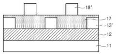
도 1a 및 도 1b를 참조하면, 반도체 기판(11)의 피식각층(12) 상부에 제1 하드마스크층(13), 제1 반사방지막(14) 및 제1 감광막(15)을 순차적으로 형성한 후, 제1 노광마스크(16)를 이용하여 전체 표면의 제1 영역을 노광하고, 노광된 제1 감광막(15)을 현상하여 제1 감광막 패턴(15')을 형성한다. 이때, 상기 하드마스크층은 통상 비정질 탄소층 및 무기계 하드마스크층의 2중층으로 구성되어 있다.1A and 1B, a first
도 1c 및 도 1d를 참조하면, 상기 제1 감광막 패턴(15')을 식각마스크로 하부 제1 반사방지막(14)을 식각하여 제1 반사방지막 패턴(14')을 형성한 후, 상기 제1 반사방지막 패턴(14')을 식각마스크로 제1 하드마스크층(13)을 식각하여 제1 하드마스크 패턴(13')을 형성한다.1C and 1D, a first anti-reflective film pattern 14 'is formed by etching the lower first
도 1e 및 도 1f를 참조하면, 제1 하드마스크 패턴(13') 상부에 제2 하드마스크층(17), 제2 반사방지막(18) 및 제2 감광막(19)을 순차적으로 형성한 후, 제2 노광마스크(20)를 이용하여 상기 제1 영역과 겹치지 않도록 교번으로 전체 표면의 제2 영역을 노광하고 상기 제2 감광막(19)을 현상하여 제2 감광막 패턴(19')을 형성한다. 이때, 상기 제2 하드마스크층(17)은 제1 하드마스크층(13)과 식각선택비가 다른 물질을 사용하는 것이 바람직하다.Referring to FIGS. 1E and 1F, a second
도 1g 및 도 1h를 참조하면, 상기 제2 감광막 패턴(19')을 식각마스크로 하부 제2 반사방지막(18)을 식각하여 제2 반사방지막 패턴(18')을 형성한 후, 상기 제2 반사방지막 패턴(18')을 식각마스크로 제2 하드마스크층(17)을 식각하여 제2 하드마스크 패턴(17')을 형성한다.Referring to FIGS. 1G and 1H, a second anti-reflection film pattern 18 'is formed by etching the second lower
도 1i를 참조하면, 제1 및 제2 하드마스크 패턴(13',17')을 식각마스크로 하부 피식각층을 식각한 후, 상기 제1 및 제2 하드마스크 패턴(13',17')을 제거하여 원하는 미세패턴을 형성한다.Referring to FIG. 1I, the first and second hard mask patterns 13 'and 17' are etched using an etching mask, and then the first and second hard mask patterns 13 'and 17' To form a desired fine pattern.
그러나, 상술한 종래 기술에 따른 반도체 소자의 미세 패턴 형성 방법의 경우, 감광막, 반사방지막 및 하드마스크층에 대하여 각각 2차례 코팅 및 식각공정을 수행하여야 하므로, 공정이 복잡하여 수율이 감소되는 문제점이 있었다.However, in the case of the conventional method of forming a fine pattern of a semiconductor device, a coating and an etching process must be performed twice for each of a photoresist layer, an antireflection layer, and a hard mask layer, there was.
상기 문제점을 해결하기 위하여, 본 발명은 실리콘이 함유된 감광막을 형성한 후 O2 플라즈마 공정을 수행하여 감광막을 제외한 코팅 및 식각 공정을 1회만 수행함으로써 공정을 단순화시켜 시간 및 비용을 감소시키는 반도체 소자의 제조 방법을 제공하는 것을 그 목적으로 한다.In order to solve the above problems, the present invention provides a method of manufacturing a semiconductor device which reduces time and cost by simplifying a process by performing an O2 plasma process after forming a silicon-containing photoresist film, And a method for producing the same.
본 발명에 따른 반도체 소자의 제조 방법은A method of manufacturing a semiconductor device according to the present invention includes:
(1) 반도체 기판 상부에 피식각층, 하드마스크층, 반사방지막 및 실리콘을 포함하는 제1 감광막을 순차적으로 형성하는 단계;(1) sequentially forming a first photoresist layer including a pattern layer, a hard mask layer, an antireflection layer, and silicon on a semiconductor substrate;
(2) 상기 제1 감광막을 제1 노광마스크를 이용하여 노광한 후 현상하여 제1 감광막 패턴을 형성하는 단계;(2) forming a first photoresist pattern by exposing the first photoresist layer using a first exposure mask and developing the first photoresist layer;
(3) 상기 제1 감광막 패턴에 02 플라즈마를 처리하는 단계;(3) treating the first photosensitive film pattern with 02 plasma;
(4) 상기 결과물 상부에 제2 감광막을 형성하고, 제2 노광마스크를 이용하여 제1 감광막 패턴과 겹치지 않는 제2 감광막 패턴을 형성하는 단계;(4) forming a second photosensitive film on the resultant product and forming a second photosensitive film pattern not overlapping the first photosensitive film pattern using a second exposure mask;
(5) 상기 제 1 및 제2 감광막 패턴을 마스크로 반사방지막을 식각한 후 상기 제 1 및 제2 감광막 패턴을 제거하여 반사방지막 패턴을 형성하는 단계; 및(5) etching the first and second photoresist patterns with a mask to remove the first and second photoresist patterns to form an antireflection pattern; And
(6) 상기 반사방지막 패턴을 식각마스크로 상기 하드마스크층을 식각하여 하드마스크 패턴을 형성한 후, 상기 하드마스크 패턴을 식각마스크로 상기 피식각층을 식각하여 피식각층 패턴을 형성하는 단계를 포함한다.(6) forming a hard mask pattern by etching the hard mask layer using the anti-reflection film pattern as an etching mask, and etching the etching layer with the hard mask pattern as an etching mask to form a pattern layer .
본 발명에서는 소정 함량의 실리콘을 함유하는 감광막을 사용하여 제1 감광막 패턴을 형성하고, 이후 02 플라즈마를 처리하여 제1 감광막 패턴 내의 실리콘을 산화시킴으로써, 제2 감광막을 도포한 후 행해지는 후속 현상 공정에서 상기 제1 감광막 패턴이 현상되지 않도록 하여 공정 단계를 줄일 수 있다는 것을 특징으로 한다. 상기에서, 실리콘은 전체 감광막에 대해 10 내지 40 중량%, 바람직하게는 20 내지 30%의 함량으로 포함된다. 또한, 상기 제2 감광막은 상기 제1 감광막과 동일하거나 또는 상이한 물질로 형성해도 무방하며, 통상적으로 사용되는 임의의 포토레지스트 조성물을 제한없이 사용할 수 있다. 이때, '상이한 물질'이란 제1 감광막과는 달리 실리콘을 함유하지 않는 임의의 포토레지스트 조성물을 의미하는 것으로서, 특정한 포토레지스트 조성물에 한정되는 것은 아니다.In the present invention, a first photosensitive film pattern is formed using a photoresist film containing a predetermined amount of silicon, and then a 02 plasma is processed to oxidize silicon in the first photosensitive film pattern, whereby a subsequent phenomenon after the second photosensitive film is applied The first photoresist pattern is not developed in the process, and the process steps can be reduced. In the above, silicon is contained in an amount of 10 to 40% by weight, preferably 20 to 30%, based on the entire photosensitive film. The second photoresist layer may be formed of the same or different material as the first photoresist layer, and any conventional photoresist composition may be used without limitation. Here, 'different material' means any photoresist composition not containing silicon unlike the first photoresist film, and is not limited to a specific photoresist composition.
한편, 실리콘을 함유하는 상기 포토레지스트 조성물로는 종래의 유기 포토레지스트 조성물과 마찬가지로 가교 결합이 이루어지도록 설계된 포토레지스트 폴리머, 광산발생제 및 유기용매를 포함하는 조성물이 제한없이 사용될 수 있다. 이러한 실리콘-함유 포토레지스트 조성물은 가교 반응을 활성화시키기 위해 열처리시 가교가 될 수 있는 가교제를 더 함유해도 무방하다.On the other hand, as the photoresist composition containing silicon, a composition including a photoresist polymer, a photoacid generator, and an organic solvent, which are designed to be crosslinked similarly to conventional organic photoresist compositions, may be used without limitation. Such a silicon-containing photoresist composition may further contain a cross-linking agent capable of cross-linking during heat treatment to activate the cross-linking reaction.
이하, 본 발명을 첨부한 도면을 참조하여 상세히 설명한다.Hereinafter, the present invention will be described in detail with reference to the accompanying drawings.
도 2a 내지 도 2h는 본 발명에 따른 반도체 소자의 제조 방법을 도시한 단면도들이다.2A to 2H are cross-sectional views illustrating a method of manufacturing a semiconductor device according to the present invention.
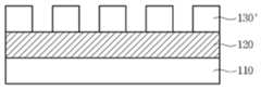
도 2a 및 도 2b를 참조하면, 반도체 기판(110) 상부에 피식각층(120), 하드마스크층(130), 반사방지막(140) 및 제1 감광막(150)을 순차적으로 형성한 후, 제1 노광마스크(160)를 이용하여 전체 표면의 제1 영역을 노광하고 상기 제1 감광막(150)을 현상하여 제1 감광막 패턴(150')을 형성한다. 이때, 제1 감광막(150)은 10 내지 40 중량%의 실리콘이 함유된 물질로 형성하는 것이 바람직하며, 또한 상기 하드마스크층(130)은 비정질 탄소층 및 무기계 하드마스크층의 2중층으로 구성되어 있는 것이 바람직하다. 아울러, 상기 노광원으로는 400 nm 이하의 파장을 가지는 모든 광원, 구체적으로는 ArF (193 nm), KrF (248 nm), EUV (Extreme Ultra Violet), VUV (Vacuum Ultra Violet, 157 nm), E-빔, X-선 및 이온빔으로 구성된 군으로부터 선택되는 광원이 제한없이 사용될 수 있으며, 노광 공정은 사용되는 감광제의 종류에 따라 다르지만 통상적으로 70 내지 150 mJ/㎠, 바람직하게는 100 mJ/㎠의 노광에너지로 수행되는 것이 바람직하다. 이중에서 노광원으로는 ArF, KrF 또는 VUV를 사용하는 것이 바람직하고, ArF를 사용하는 것이 더욱 바람직하다.2A and 2B, the
도 2c를 참조하면, 전체 표면에 02 플라즈마 처리 공정을 수행하여 제1 감광막 패턴(150') 내의 실리콘을 산화시킴으로써, SiO2로 변형된 제1 감광막 패턴(155)을 형성한다.Referring to FIG. 2C, a SiO2 modified first
도 2d 및 도 2e를 참조하면, 상기 SiO2-포함 제1 감광막 패턴(155)을 포함하는 전체 표면 상부에 제2 감광막(190)을 형성한 후, 제2 노광마스크(200)를 이용하여 제1 감광막 패턴(150)과 겹치지 않도록 상호 교번적으로 전체 표면의 제2 영역을 노광 후 현상하여 제2 감광막 패턴(190')을 형성한다. 이때, 상기 제1 감광막 패턴(155)은 O2 플라즈마 처리에 의해 내부에 포함된 실리콘이 SiO2로 변형되었기 때문에 현상 공정시 제거되지 않고 남아 있게 된다. 한편, 상기 제2 감광막(190)은 제1 감광막(150)과는 달리 실리콘을 함유하는 감광막을 사용하지 않아도 무방하며, 통상의 포토레지스트 조성물을 제한없이 사용할 수 있다.Referring to FIGS. 2d and 2e, a second
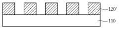
도 2f 및 도 2g를 참조하면, 제1 및 제2 감광막 패턴(155,190')을 마스크로 상기 반사방지막(140)을 식각하여 반사방지막 패턴(140')을 형성한다. 이후, 상기 반사방지막 패턴(140')을 마스크로 하드마스크층(130)을 식각한 후, 반사방지막 패턴(140')을 제거하여 하드마스크 패턴(130')을 형성한다.Referring to FIGS. 2F and 2G, the
도 2h를 참조하면, 하드마스크 패턴(130')을 마스크로 피식각층(120)을 식각한 후 하드마스크 패턴(130')을 제거하여 원하는 미세패턴(120')을 형성한다.Referring to FIG. 2H, the
본 발명에 따른 반도체 소자의 제조 방법은 실리콘이 함유된 감광막을 형성한 후 02 플라즈마 공정을 수행함으로써 감광막을 제외한 코팅 및 식각 공정은 1회만 수행하도록 하여 공정을 단순화시키며 시간 및 비용을 감소시키는 효과가 있다.In the method of manufacturing a semiconductor device according to the present invention, a 02 plasma process is performed after forming a silicon-containing photoresist film, thereby performing a coating and etching process except for the photoresist film only once, thereby simplifying the process and reducing time and cost .
아울러, 본 발명의 바람직한 실시예는 예시의 목적을 위한 것으로, 당업자라면 첨부된 특허청구범위의 기술적 사상과 범위를 통해 다양한 수정, 변경, 대체 및 부가가 가능할 것이며, 이러한 수정 변경 등은 이하의 특허청구범위에 속하는 것으로 보아야 할 것이다.It will be understood by those of ordinary skill in the art that various changes in form and details may be made therein without departing from the spirit and scope of the present invention as set forth in the following claims, It should be regarded as belonging to the claims.
Claims (7)
Translated fromKoreanPriority Applications (3)
| Application Number | Priority Date | Filing Date | Title |
|---|---|---|---|
| TW095131538ATW200725695A (en) | 2005-12-28 | 2006-08-28 | Method for manufacturing semiconductor device |
| US11/468,084US7655568B2 (en) | 2005-12-28 | 2006-08-29 | Method for manufacturing underlying pattern of semiconductor device |
| JP2006241537AJP4921898B2 (en) | 2005-12-28 | 2006-09-06 | Manufacturing method of semiconductor device |
Applications Claiming Priority (2)
| Application Number | Priority Date | Filing Date | Title |
|---|---|---|---|
| KR1020050132110 | 2005-12-28 | ||
| KR20050132110 | 2005-12-28 |
Publications (2)
| Publication Number | Publication Date |
|---|---|
| KR20070070036A KR20070070036A (en) | 2007-07-03 |
| KR100811431B1true KR100811431B1 (en) | 2008-03-07 |
Family
ID=38214314
Family Applications (1)
| Application Number | Title | Priority Date | Filing Date |
|---|---|---|---|
| KR1020060069760AExpired - Fee RelatedKR100811431B1 (en) | 2005-12-28 | 2006-07-25 | Method of Manufacturing Semiconductor Device |
Country Status (5)
| Country | Link |
|---|---|
| US (1) | US7655568B2 (en) |
| JP (1) | JP4921898B2 (en) |
| KR (1) | KR100811431B1 (en) |
| CN (1) | CN100477080C (en) |
| TW (1) | TW200725695A (en) |
Families Citing this family (18)
| Publication number | Priority date | Publication date | Assignee | Title |
|---|---|---|---|---|
| US7807336B2 (en)* | 2005-12-28 | 2010-10-05 | Hynix Semiconductor Inc. | Method for manufacturing semiconductor device |
| US7959818B2 (en)* | 2006-09-12 | 2011-06-14 | Hynix Semiconductor Inc. | Method for forming a fine pattern of a semiconductor device |
| KR100798738B1 (en)* | 2006-09-28 | 2008-01-29 | 주식회사 하이닉스반도체 | Manufacturing method of fine pattern of semiconductor device |
| KR100912959B1 (en)* | 2006-11-09 | 2009-08-20 | 주식회사 하이닉스반도체 | Manufacturing method of fine pattern of semiconductor device |
| KR100819673B1 (en)* | 2006-12-22 | 2008-04-04 | 주식회사 하이닉스반도체 | Semiconductor element and pattern formation method thereof |
| KR100876816B1 (en)* | 2007-06-29 | 2009-01-07 | 주식회사 하이닉스반도체 | Method of forming fine pattern of semiconductor device |
| US8124323B2 (en)* | 2007-09-25 | 2012-02-28 | Taiwan Semiconductor Manufacturing Company, Ltd. | Method for patterning a photosensitive layer |
| US7935477B2 (en)* | 2007-11-30 | 2011-05-03 | Taiwan Semiconductor Manufacturing Company, Ltd. | Double patterning strategy for contact hole and trench |
| JP5192795B2 (en)* | 2007-12-06 | 2013-05-08 | 株式会社日立ハイテクノロジーズ | Electron beam measuring device |
| JP2009283674A (en)* | 2008-05-22 | 2009-12-03 | Elpida Memory Inc | Method of manufacturing semiconductor apparatus |
| US8293460B2 (en)* | 2008-06-16 | 2012-10-23 | Applied Materials, Inc. | Double exposure patterning with carbonaceous hardmask |
| KR101523951B1 (en)* | 2008-10-09 | 2015-06-02 | 삼성전자주식회사 | Method for forming fine pattern of semiconductor device |
| US8551689B2 (en)* | 2010-05-27 | 2013-10-08 | Samsung Electronics Co., Ltd. | Methods of manufacturing semiconductor devices using photolithography |
| KR101658492B1 (en)* | 2010-08-13 | 2016-09-21 | 삼성전자주식회사 | Method for forming fine patterns and method for manufacturing a semiconductor device by using the same |
| KR101215645B1 (en)* | 2010-12-09 | 2012-12-26 | 에스케이하이닉스 주식회사 | Overlay vernier mask pattern, methof for fabricating the same, semicondcutor device having the overlay vernier pattern, and method of fabricating the semiconductor device |
| CN103309165A (en)* | 2012-03-09 | 2013-09-18 | 中芯国际集成电路制造(上海)有限公司 | Formation method for semiconductor structure |
| KR101926418B1 (en)* | 2012-05-16 | 2018-12-10 | 삼성전자주식회사 | method for manufacturing a semiconductor device |
| KR102270137B1 (en)* | 2017-11-29 | 2021-06-28 | 삼성에스디아이 주식회사 | Method of forming patterns |
Citations (4)
| Publication number | Priority date | Publication date | Assignee | Title |
|---|---|---|---|---|
| JPH04176123A (en)* | 1990-11-08 | 1992-06-23 | Nec Corp | Manufacture of semiconductor device |
| KR19980028362A (en)* | 1996-10-22 | 1998-07-15 | 김영환 | Manufacturing method of fine pattern of semiconductor device |
| KR19990061090A (en)* | 1997-12-31 | 1999-07-26 | 김영환 | Photoresist for multilayer resist process and fine pattern manufacturing method of semiconductor device using same |
| KR20050119910A (en)* | 2004-06-17 | 2005-12-22 | 삼성전자주식회사 | Method of forming semiconductor patterns |
Family Cites Families (13)
| Publication number | Priority date | Publication date | Assignee | Title |
|---|---|---|---|---|
| US5186788A (en)* | 1987-07-23 | 1993-02-16 | Matsushita Electric Industrial Co., Ltd. | Fine pattern forming method |
| US5667940A (en)* | 1994-05-11 | 1997-09-16 | United Microelectronics Corporation | Process for creating high density integrated circuits utilizing double coating photoresist mask |
| KR100206597B1 (en)* | 1995-12-29 | 1999-07-01 | 김영환 | Manufacturing method of fine pattern of semiconductor device |
| JP2000077317A (en)* | 1998-09-03 | 2000-03-14 | Sony Corp | Forming method of resist pattern |
| US6140023A (en)* | 1998-12-01 | 2000-10-31 | Advanced Micro Devices, Inc. | Method for transferring patterns created by lithography |
| US6586339B1 (en)* | 1999-10-28 | 2003-07-01 | Advanced Micro Devices, Inc. | Silicon barrier layer to prevent resist poisoning |
| US6534414B1 (en)* | 2000-06-14 | 2003-03-18 | Integrated Device Technology, Inc. | Dual-mask etch of dual-poly gate in CMOS processing |
| TWI245774B (en)* | 2001-03-01 | 2005-12-21 | Shinetsu Chemical Co | Silicon-containing polymer, resist composition and patterning process |
| JP4342767B2 (en)* | 2002-04-23 | 2009-10-14 | 富士通マイクロエレクトロニクス株式会社 | Manufacturing method of semiconductor device |
| DE10223997A1 (en)* | 2002-05-29 | 2003-12-18 | Infineon Technologies Ag | Process for the production of photomasks for structuring semiconductor substrates by optical lithography |
| JP2004153073A (en)* | 2002-10-31 | 2004-05-27 | Renesas Technology Corp | Manufacture of semiconductor device |
| KR100971976B1 (en) | 2003-07-24 | 2010-07-22 | 주식회사 포스코 | Surface roughness equalizer of galvanized steel strip |
| KR100510558B1 (en)* | 2003-12-13 | 2005-08-26 | 삼성전자주식회사 | Method for forming pattern |
- 2006
- 2006-07-25KRKR1020060069760Apatent/KR100811431B1/ennot_activeExpired - Fee Related
- 2006-08-28TWTW095131538Apatent/TW200725695A/enunknown
- 2006-08-29USUS11/468,084patent/US7655568B2/ennot_activeExpired - Fee Related
- 2006-09-06JPJP2006241537Apatent/JP4921898B2/ennot_activeExpired - Fee Related
- 2006-09-11CNCNB2006101515481Apatent/CN100477080C/ennot_activeExpired - Fee Related
Patent Citations (4)
| Publication number | Priority date | Publication date | Assignee | Title |
|---|---|---|---|---|
| JPH04176123A (en)* | 1990-11-08 | 1992-06-23 | Nec Corp | Manufacture of semiconductor device |
| KR19980028362A (en)* | 1996-10-22 | 1998-07-15 | 김영환 | Manufacturing method of fine pattern of semiconductor device |
| KR19990061090A (en)* | 1997-12-31 | 1999-07-26 | 김영환 | Photoresist for multilayer resist process and fine pattern manufacturing method of semiconductor device using same |
| KR20050119910A (en)* | 2004-06-17 | 2005-12-22 | 삼성전자주식회사 | Method of forming semiconductor patterns |
Also Published As
| Publication number | Publication date |
|---|---|
| JP2007180489A (en) | 2007-07-12 |
| CN100477080C (en) | 2009-04-08 |
| US20070148983A1 (en) | 2007-06-28 |
| US7655568B2 (en) | 2010-02-02 |
| TW200725695A (en) | 2007-07-01 |
| CN1992155A (en) | 2007-07-04 |
| JP4921898B2 (en) | 2012-04-25 |
| KR20070070036A (en) | 2007-07-03 |
Similar Documents
| Publication | Publication Date | Title |
|---|---|---|
| KR100811431B1 (en) | Method of Manufacturing Semiconductor Device | |
| TWI387998B (en) | A lithography method | |
| TW201800861A (en) | Lithography patterning method | |
| US8158332B2 (en) | Method of manufacturing a semiconductor device | |
| JP2013135066A (en) | Pattern forming method | |
| US8822347B2 (en) | Wet soluble lithography | |
| KR20190064504A (en) | Anti-reflective coating by ion implantation for lithography patterning | |
| CN108231548B (en) | Method for manufacturing semiconductor device | |
| JP2004530922A (en) | Process for forming sublithographic photoresist features | |
| CN108983546A (en) | Lithographic method | |
| JP2008258562A (en) | Pattern formation method | |
| KR100772801B1 (en) | Method of Manufacturing Semiconductor Device | |
| CN108333866B (en) | Method of photolithographic patterning | |
| KR100415091B1 (en) | method for manufacturing fine pattern | |
| US7807336B2 (en) | Method for manufacturing semiconductor device | |
| TWI742010B (en) | Lithography method and photoresist | |
| JP2009194207A (en) | Pattern forming method, and manufacturing method for semiconductor device and semiconductor device manufacturing apparatus | |
| KR20100042421A (en) | Method for forming pattern of semiconductor device | |
| US20030228538A1 (en) | E-beam curable resist and process for e-beam curing the resist | |
| KR19980028359A (en) | Manufacturing method of fine pattern of semiconductor device | |
| KR20050038125A (en) | Forming method of fine contact hole | |
| KR20050003603A (en) | Forming method of fine pattern | |
| Guerrero et al. | Resist double patterning on BARCs and spin-on multilayer materials | |
| KR100604755B1 (en) | Pattern Forming Method Using Photoresist Curing | |
| KR20080092154A (en) | Method of forming fine pattern of semiconductor device |
Legal Events
| Date | Code | Title | Description |
|---|---|---|---|
| PA0109 | Patent application | St.27 status event code:A-0-1-A10-A12-nap-PA0109 | |
| A201 | Request for examination | ||
| PA0201 | Request for examination | St.27 status event code:A-1-2-D10-D11-exm-PA0201 | |
| PG1501 | Laying open of application | St.27 status event code:A-1-1-Q10-Q12-nap-PG1501 | |
| D13-X000 | Search requested | St.27 status event code:A-1-2-D10-D13-srh-X000 | |
| D14-X000 | Search report completed | St.27 status event code:A-1-2-D10-D14-srh-X000 | |
| E902 | Notification of reason for refusal | ||
| PE0902 | Notice of grounds for rejection | St.27 status event code:A-1-2-D10-D21-exm-PE0902 | |
| P11-X000 | Amendment of application requested | St.27 status event code:A-2-2-P10-P11-nap-X000 | |
| P13-X000 | Application amended | St.27 status event code:A-2-2-P10-P13-nap-X000 | |
| E701 | Decision to grant or registration of patent right | ||
| PE0701 | Decision of registration | St.27 status event code:A-1-2-D10-D22-exm-PE0701 | |
| GRNT | Written decision to grant | ||
| PR0701 | Registration of establishment | St.27 status event code:A-2-4-F10-F11-exm-PR0701 | |
| PR1002 | Payment of registration fee | St.27 status event code:A-2-2-U10-U11-oth-PR1002 Fee payment year number:1 | |
| PG1601 | Publication of registration | St.27 status event code:A-4-4-Q10-Q13-nap-PG1601 | |
| G170 | Re-publication after modification of scope of protection [patent] | ||
| PG1701 | Publication of correction | St.27 status event code:A-5-5-P10-P19-oth-PG1701 Patent document republication publication date:20080410 Republication note text:Request for Correction Notice (Document Request) Gazette number:1008114310000 Gazette reference publication date:20080307 | |
| PR1001 | Payment of annual fee | St.27 status event code:A-4-4-U10-U11-oth-PR1001 Fee payment year number:4 | |
| FPAY | Annual fee payment | Payment date:20120127 Year of fee payment:5 | |
| PR1001 | Payment of annual fee | St.27 status event code:A-4-4-U10-U11-oth-PR1001 Fee payment year number:5 | |
| PN2301 | Change of applicant | St.27 status event code:A-5-5-R10-R13-asn-PN2301 St.27 status event code:A-5-5-R10-R11-asn-PN2301 | |
| PN2301 | Change of applicant | St.27 status event code:A-5-5-R10-R13-asn-PN2301 St.27 status event code:A-5-5-R10-R11-asn-PN2301 | |
| LAPS | Lapse due to unpaid annual fee | ||
| PC1903 | Unpaid annual fee | St.27 status event code:A-4-4-U10-U13-oth-PC1903 Not in force date:20130301 Payment event data comment text:Termination Category : DEFAULT_OF_REGISTRATION_FEE | |
| PC1903 | Unpaid annual fee | St.27 status event code:N-4-6-H10-H13-oth-PC1903 Ip right cessation event data comment text:Termination Category : DEFAULT_OF_REGISTRATION_FEE Not in force date:20130301 | |
| PN2301 | Change of applicant | St.27 status event code:A-5-5-R10-R13-asn-PN2301 St.27 status event code:A-5-5-R10-R11-asn-PN2301 |