KR100810060B1 - Semiconductor memory device and driving method thereof - Google Patents
Semiconductor memory device and driving method thereofDownload PDFInfo
- Publication number
- KR100810060B1 KR100810060B1KR1020060034104AKR20060034104AKR100810060B1KR 100810060 B1KR100810060 B1KR 100810060B1KR 1020060034104 AKR1020060034104 AKR 1020060034104AKR 20060034104 AKR20060034104 AKR 20060034104AKR 100810060 B1KR100810060 B1KR 100810060B1
- Authority
- KR
- South Korea
- Prior art keywords
- refresh
- row
- self
- mode
- stored value
- Prior art date
- Legal status (The legal status is an assumption and is not a legal conclusion. Google has not performed a legal analysis and makes no representation as to the accuracy of the status listed.)
- Expired - Fee Related
Links
Images


Classifications
- G—PHYSICS
- G11—INFORMATION STORAGE
- G11C—STATIC STORES
- G11C11/00—Digital stores characterised by the use of particular electric or magnetic storage elements; Storage elements therefor
- G11C11/21—Digital stores characterised by the use of particular electric or magnetic storage elements; Storage elements therefor using electric elements
- G11C11/34—Digital stores characterised by the use of particular electric or magnetic storage elements; Storage elements therefor using electric elements using semiconductor devices
- G11C11/40—Digital stores characterised by the use of particular electric or magnetic storage elements; Storage elements therefor using electric elements using semiconductor devices using transistors
- G11C11/401—Digital stores characterised by the use of particular electric or magnetic storage elements; Storage elements therefor using electric elements using semiconductor devices using transistors forming cells needing refreshing or charge regeneration, i.e. dynamic cells
- G11C11/406—Management or control of the refreshing or charge-regeneration cycles
- G11C11/40615—Internal triggering or timing of refresh, e.g. hidden refresh, self refresh, pseudo-SRAMs
- G—PHYSICS
- G11—INFORMATION STORAGE
- G11C—STATIC STORES
- G11C11/00—Digital stores characterised by the use of particular electric or magnetic storage elements; Storage elements therefor
- G11C11/21—Digital stores characterised by the use of particular electric or magnetic storage elements; Storage elements therefor using electric elements
- G11C11/34—Digital stores characterised by the use of particular electric or magnetic storage elements; Storage elements therefor using electric elements using semiconductor devices
- G11C11/40—Digital stores characterised by the use of particular electric or magnetic storage elements; Storage elements therefor using electric elements using semiconductor devices using transistors
- G11C11/401—Digital stores characterised by the use of particular electric or magnetic storage elements; Storage elements therefor using electric elements using semiconductor devices using transistors forming cells needing refreshing or charge regeneration, i.e. dynamic cells
- G11C11/406—Management or control of the refreshing or charge-regeneration cycles
- G11C11/40618—Refresh operations over multiple banks or interleaving
- G—PHYSICS
- G11—INFORMATION STORAGE
- G11C—STATIC STORES
- G11C11/00—Digital stores characterised by the use of particular electric or magnetic storage elements; Storage elements therefor
- G11C11/21—Digital stores characterised by the use of particular electric or magnetic storage elements; Storage elements therefor using electric elements
- G11C11/34—Digital stores characterised by the use of particular electric or magnetic storage elements; Storage elements therefor using electric elements using semiconductor devices
- G11C11/40—Digital stores characterised by the use of particular electric or magnetic storage elements; Storage elements therefor using electric elements using semiconductor devices using transistors
- G11C11/401—Digital stores characterised by the use of particular electric or magnetic storage elements; Storage elements therefor using electric elements using semiconductor devices using transistors forming cells needing refreshing or charge regeneration, i.e. dynamic cells
- G11C11/4063—Auxiliary circuits, e.g. for addressing, decoding, driving, writing, sensing or timing
- G11C11/407—Auxiliary circuits, e.g. for addressing, decoding, driving, writing, sensing or timing for memory cells of the field-effect type
- G11C11/4072—Circuits for initialization, powering up or down, clearing memory or presetting
- G—PHYSICS
- G11—INFORMATION STORAGE
- G11C—STATIC STORES
- G11C11/00—Digital stores characterised by the use of particular electric or magnetic storage elements; Storage elements therefor
- G11C11/21—Digital stores characterised by the use of particular electric or magnetic storage elements; Storage elements therefor using electric elements
- G11C11/34—Digital stores characterised by the use of particular electric or magnetic storage elements; Storage elements therefor using electric elements using semiconductor devices
- G11C11/40—Digital stores characterised by the use of particular electric or magnetic storage elements; Storage elements therefor using electric elements using semiconductor devices using transistors
- G11C11/401—Digital stores characterised by the use of particular electric or magnetic storage elements; Storage elements therefor using electric elements using semiconductor devices using transistors forming cells needing refreshing or charge regeneration, i.e. dynamic cells
- G11C11/4063—Auxiliary circuits, e.g. for addressing, decoding, driving, writing, sensing or timing
- G11C11/407—Auxiliary circuits, e.g. for addressing, decoding, driving, writing, sensing or timing for memory cells of the field-effect type
- G11C11/4076—Timing circuits
- G—PHYSICS
- G11—INFORMATION STORAGE
- G11C—STATIC STORES
- G11C11/00—Digital stores characterised by the use of particular electric or magnetic storage elements; Storage elements therefor
- G11C11/21—Digital stores characterised by the use of particular electric or magnetic storage elements; Storage elements therefor using electric elements
- G11C11/34—Digital stores characterised by the use of particular electric or magnetic storage elements; Storage elements therefor using electric elements using semiconductor devices
- G11C11/40—Digital stores characterised by the use of particular electric or magnetic storage elements; Storage elements therefor using electric elements using semiconductor devices using transistors
- G11C11/401—Digital stores characterised by the use of particular electric or magnetic storage elements; Storage elements therefor using electric elements using semiconductor devices using transistors forming cells needing refreshing or charge regeneration, i.e. dynamic cells
- G11C11/4063—Auxiliary circuits, e.g. for addressing, decoding, driving, writing, sensing or timing
- G11C11/407—Auxiliary circuits, e.g. for addressing, decoding, driving, writing, sensing or timing for memory cells of the field-effect type
- G11C11/408—Address circuits
- G—PHYSICS
- G11—INFORMATION STORAGE
- G11C—STATIC STORES
- G11C29/00—Checking stores for correct operation ; Subsequent repair; Testing stores during standby or offline operation
- G11C29/04—Detection or location of defective memory elements, e.g. cell constructio details, timing of test signals
- G11C29/50—Marginal testing, e.g. race, voltage or current testing
- G11C29/50012—Marginal testing, e.g. race, voltage or current testing of timing
- G—PHYSICS
- G11—INFORMATION STORAGE
- G11C—STATIC STORES
- G11C29/00—Checking stores for correct operation ; Subsequent repair; Testing stores during standby or offline operation
- G11C29/04—Detection or location of defective memory elements, e.g. cell constructio details, timing of test signals
- G11C29/50—Marginal testing, e.g. race, voltage or current testing
- G11C29/50016—Marginal testing, e.g. race, voltage or current testing of retention
- G—PHYSICS
- G11—INFORMATION STORAGE
- G11C—STATIC STORES
- G11C7/00—Arrangements for writing information into, or reading information out from, a digital store
- G11C7/20—Memory cell initialisation circuits, e.g. when powering up or down, memory clear, latent image memory
- G—PHYSICS
- G11—INFORMATION STORAGE
- G11C—STATIC STORES
- G11C2211/00—Indexing scheme relating to digital stores characterized by the use of particular electric or magnetic storage elements; Storage elements therefor
- G11C2211/401—Indexing scheme relating to cells needing refreshing or charge regeneration, i.e. dynamic cells
- G11C2211/406—Refreshing of dynamic cells
- G11C2211/4061—Calibration or ate or cycle tuning
Landscapes
- Engineering & Computer Science (AREA)
- Microelectronics & Electronic Packaging (AREA)
- Computer Hardware Design (AREA)
- Dram (AREA)
- Read Only Memory (AREA)
Abstract
Translated fromKoreanDescription
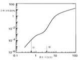
Translated fromKorean도 1은 칩 리프레시 타임에 따른 오류 비트율 특성을 나타낸 그래프.1 is a graph showing an error bit rate characteristic according to a chip refresh time.
도 2는 종래의 이중 주기 셀프 리프레시 방식을 설명하기 위한 도면.2 is a diagram for explaining a conventional double-cycle self-refresh method.
도 3은 칩 리프레시 타임과 리프레시 타임 특성이 양호한 로우의 리프레시 타임의 관계를 나타낸 도면.Fig. 3 is a diagram showing a relationship of a refresh time of a row having a good chip refresh time and refresh time characteristics; Fig.
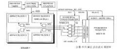
도 4는 본 발명에 따른 DRAM의 셀프 리프레시 경로를 예시한 블럭 다이어그램.4 is a block diagram illustrating a self-refresh path of a DRAM according to the present invention.
도 5는 본 발명에 따른 DRAM의 특징적 구성 및 동작을 개념적으로 나타낸 도면.FIG. 5 conceptually illustrates a characteristic configuration and operation of a DRAM according to the present invention; FIG.
도 6은 설정 리프레시 주기신호에 따른 셀프 리프레시 동작상의 변화를 설명하기 위한 도면.6 is a diagram for explaining a change in the self-refresh operation according to the set refresh period signal;
도 7은 본 발명의 제1 실시예에 따른 반도체 메모리 소자의 셀프 리프레시 동작을 나타낸 도면.7 is a view showing a self-refresh operation of the semiconductor memory device according to the first embodiment of the present invention.
도 8은 본 발명의 제2 실시예에 따른 반도체 메모리 소자의 셀프 리프레시 동작을 나타낸 도면.8 is a view showing a self-refresh operation of the semiconductor memory device according to the second embodiment of the present invention.
도 9는 셀프 리프레시 방식에 따른 셀프 리프레시 전류 특성을 나타낸 그래프.9 is a graph showing a self-refresh current characteristic according to the self-refresh method.
본 발명은 반도체 회로 설계 기술에 관한 것으로, 특히 반도체 메모리 소자의 셀프 리프레시 관련 기술에 관한 것이다.BACKGROUND OF THE
반도체 메모리 소자 중에서도 DRAM은 SRAM이나 플래쉬 메모리와 달리 시간이 흐름에 따라 메모리 셀(입력된 정보를 저장하는 단위 유닛)에 저장된 정보가 사라지는 현상이 발생한다. 이러한 현상을 방지하기 위하여 외부에서 일정 주기마다 셀에 저장된 정보를 다시 기입해주는 동작을 수행하도록 하고 있으며, 이러한 과정을 리프레시 동작이라 한다. 리프레시 동작은 메모리 셀 어레이 안의 각 셀들이 가지는 리텐션 시간(retention time) 안에 적어도 한 번씩 워드라인을 띄워 셀의 데이터를 센싱하여 증폭시킨 후 셀에 재기록하는 방식으로 행해진다. 여기서, 리텐션 시간이란 셀에 어떤 데이터를 기록한 후 리프레시 없이 데이터가 셀에서 유지될 수 있는 시간을 말한다.Among the semiconductor memory devices, unlike the SRAM and the flash memory, the information stored in the memory cells (unit units storing the input information) disappears over time. In order to prevent such a phenomenon, an operation of rewriting information stored in a cell every predetermined period is performed externally, and this process is referred to as a refresh operation. The refresh operation is performed by sensing the data of the cell by floating the word line at least once within the retention time of each cell in the memory cell array, amplifying it, and then rewriting it in the cell. Here, the retention time refers to the time that data can be held in a cell without refreshing after data is written to the cell.
리프레시 모드에는 노말 동작 중에 특정 조합의 커맨드 신호를 주기적으로 띄워 내부적으로 어드레스를 생성하여 해당 셀에 대한 리프레시를 수행하는 오토 리프레시 모드와, 노말 동작을 하지 않는 대기 상태, 예컨대 파워다운 모드에서 내 부적으로 커맨드를 생성하여 수행하는 셀프 리프레시 모드가 있다. 오토 리프레시 모드와 셀프 리프레시 모드는 모두 커맨드를 받은 후 내부 카운터로부터 어드레스를 생성하여 수행되며, 요청이 들어올 때마다 이 어드레스가 순차적으로 증가하게 된다. 한편, 셀프 리프레시 모드는 노트북, PDA, 이동통신 단말기 등의 모바일 장치용 로우(low) 파워 DRAM에서는 거의 필수적으로 채택되고 있다.The refresh mode includes an auto refresh mode in which an address is internally generated by periodically floating a command signal of a specific combination during a normal operation and an auto refresh mode in which an address is internally generated in a standby state in which normal operation is not performed, There is a self-refresh mode in which a command is generated and executed. Both the auto-refresh mode and the self-refresh mode are performed by generating an address from the internal counter after receiving a command, and the address is sequentially incremented each time a request is received. On the other hand, the self-refresh mode is almost indispensable in low power DRAMs for mobile devices such as notebook computers, PDAs, and mobile communication terminals.
통상적으로, 셀프 리프레시 모드에서는 칩 내부의 링 오실레이터로부터 출력되는 주기 신호(또는 주기 신호를 분주한 신호)에 의해 리프레시 주기(tREF)가 결정된다. 이 리프레시 주기(tREF)는 테스트를 통해 파악된 해당 칩의 리프레시 타임 특성에 따라 결정된다. 리프레시 타임 특성은 각 로우(row)별로 다르게 나타나는데, 비트 오류(bit fail)을 방지하기 위해서는 최악의 리프레시 타임 특성을 가진 로우를 기준으로 리프레시 주기(tREF)를 결정할 수밖에 없었다.Normally, in the self-refresh mode, the refresh period (tREF) is determined by the periodic signal output from the ring oscillator in the chip (or a signal obtained by dividing the periodic signal). This refresh period tREF is determined according to the refresh time characteristic of the chip identified through the test. The refresh time characteristics are different for each row. In order to prevent a bit failure, the refresh period tREF has to be determined based on the row having the worst refresh time characteristic.
도 1은 칩 리프레시 타임에 따른 오류 비트율 특성을 나타낸 그래프이다.1 is a graph showing an error bit rate characteristic according to a chip refresh time.
도 1을 참조하면, 칩의 리프레시 타임(t1)은 최악의 리프레시 타임 특성을 가진 로우를 기준으로 결정되기 때문에 양호한 로우의 리프레시 타임(t2)에 비해 몇 배 정도 차이를 가지게 된다. 즉, 칩의 리프레시 타임(t1)은 각 로우별 리프레시 타임 특성보다 나쁘게 설정될 수밖에 없어 불필요한 전류 소모가 발생하게 된다.Referring to FIG. 1, since the refresh time t1 of the chip is determined on the basis of the row having the worst refresh time characteristic, the refresh time t2 is several times larger than the refresh time t2 of a good row. That is, the refresh time t1 of the chip is set to be worse than the refresh time characteristic for each row, resulting in unnecessary current consumption.
한편, 상기와 같은 셀프 리프레시 모드에서의 불필요한 전류 소모를 줄이기 위하여 이중 주기 셀프 리프레시 방식이 제안된 바 있다.Meanwhile, in order to reduce unnecessary current consumption in the self-refresh mode, a dual-cycle self-refresh method has been proposed.
도 2는 종래의 이중 주기 셀프 리프레시 방식을 설명하기 위한 도면이다. 도 2에 도시된 내용은 기 발표된 논문['Dual-Period Self-Refresh Scheme for Low-Power DRAM's with On-Chip PROM Mode Register', IEEE JOURNAL OF SOLID STATE CIRCUIT, VOL.33, NO.2, FEBRUARY 1998.]에 자세히 설명되어 있어 그 상세 구성 및 동작에 대한 설명은 생략하기로 한다.2 is a diagram for explaining a conventional dual-cycle self-refresh method. The contents shown in FIG. 2 are described in a document ['Dual-Period Self-Refresh Scheme for Low-Power DRAM with On-Chip PROM Mode Register', IEEE JOURNAL OF SOLID STATE CIRCUIT, Vol.33, NO.2, FEBRUARY 1998.], and a detailed description thereof will be omitted.
다만, 이중 주기 셀프 리프레시 주기 제어부의 PROM 모드 레지스터에 각 로우별 리프레시 타임 특성을 저장하고, 저장된 정보와 리프레시 어드레스를 이용하여 DRAM부의 각 셀 어레이 블럭에 대하여 두 개의 리프레시 주기를 선택적으로 적용하고 있음을 도면을 통해 쉽게 파악할 수 있다.However, the refresh time characteristic for each row is stored in the PROM mode register of the dual period self refresh period control unit, and two refresh periods are selectively applied to each cell array block of the DRAM unit using the stored information and the refresh address It can be easily grasped through the drawings.
상기와 같은 이중 주기 셀프 리프레시 방식을 적용하는 경우, 단일 주기 셀프 리프레시 방식에 비해 불필요한 전류 소모를 줄일 수 있다. 그러나, 이 기술은 리프레시 주기 제어부에서 비휘발성 메모리인 PROM(Programmable Read Only Memory)을 사용하고 있는 바, 이러한 PROM을 DRAM 칩 내에 실장하는 것이 실질적으로 불가능하기 때문에 실현성이 없는 기술이라는 한계가 있었다.When the dual-cycle self-refresh scheme as described above is applied, unnecessary current consumption can be reduced as compared with the single-cycle self-refresh scheme. However, this technique uses a PROM (Programmable Read Only Memory), which is a nonvolatile memory, in the refresh cycle control section, and it is practically impossible to implement such a PROM in a DRAM chip.
본 발명은 상기와 같은 종래기술의 문제점을 해결하기 위하여 제안된 것으로, 셀프 리프레시 모드에서의 불필요한 전류 소모를 최소화할 수 있는 반도체 메모리 소자 및 그의 구동방법을 제공하는데 그 목적이 있다.SUMMARY OF THE INVENTION It is an object of the present invention to provide a semiconductor memory device capable of minimizing unnecessary current consumption in a self-refresh mode and a driving method thereof.
상기의 기술적 과제를 달성하기 위한 본 발명의 일 측면에 따르면, 메모리 셀 어레이를 이루는 각 로우의 리프레시 타임 특성 - 셀프 리프레시 모드 중에 수행되는 자체 테스트 결과에 따라 결정됨 - 을 저장하기 위한 다수의 제1 저장수단; 상기 자체 테스트 과정에서 선택된 로우의 데이터를 임시 저장하기 위한 다수의 제2 저장수단; 셀프 리프레시 모드에서 최소 리프레시 주기신호를 생성하기 위한 발진수단; 셀프 리프레시 모드에서 순차적인 내부 리프레시 어드레스를 생성하기 위한 카운팅 수단; 및 설정 리프레시 주기신호를 생성하기 위한 리프레시 주기 제어수단을 구비하여, 해당 로우에 대응하는 제1 저장수단의 값과 상기 설정 리프레시 주기신호에 따라 해당 로우에 대한 리프레시 수행/생략 여부를 결정하는 것을 특징으로 하는 반도체 메모리 소자가 제공된다.According to an aspect of the present invention, there is provided a semiconductor memory device comprising: a plurality of first storage units for storing a refresh time characteristic of each row of a memory cell array, which is determined according to a self test result performed during a self- Way; A plurality of second storage means for temporarily storing data of a selected row in the self test process; Oscillation means for generating a minimum refresh period signal in the self refresh mode; Counting means for generating a sequential internal refresh address in the self-refresh mode; And a refresh cycle control means for generating a set refresh cycle signal so as to determine whether to perform refresh / omission of the row in accordance with the value of the first storage means corresponding to the row and the set refresh period signal Is provided.
또한, 본 발명의 다른 측면에 따르면, 메모리 셀 어레이를 이루는 각 로우의 리프레시 타임 특성에 대응하는 제1 저장값을 초기화하는 제1 단계; 셀프 리프레시 모드 진입 후, 첫 로우의 각 컬럼에 대응하는 데이터를 제2 저장값으로서 저장하는 제2 단계; 리프레시 사이클을 다수번 진행하면서 상기 첫 로우에 대한 리프레시 주기 설정을 위한 리프레시 타임 특성 자체 테스트 - 초기 리프레시 사이클 이후 예정된 리프레시 사이클동안 상기 첫 로우에 대한 리프레시를 생략하는 테스트 - 를 수행하여 그 결과에 따라 상기 첫 로우의 리프레시 타임 특성에 대응하는 상기 제1 저장값을 설정하는 제3 단계; 상기 첫 로우에 대응하는 상기 제2 저장값을 상기 각 컬럼에 대응하는 데이터로서 재저장하는 제4 단계; 및 두번째 로우에 대하여 상기 제2 내지 제4 단계를 수행하되, 상기 첫 로우에 대응하는 제1 저장값에 따라 상기 첫 로우에 대해 최소 리프레시 주기 또는 설정 리프레시 주기를 선택적으로 적용하는 제5 단계를 포함하는 반도체 메모리 소자의 구동방법이 제공된다.According to another aspect of the present invention, there is provided a memory cell array including: a first step of initializing a first stored value corresponding to a refresh time characteristic of each row constituting a memory cell array; A second step of storing, as a second stored value, data corresponding to each column of the first row after entering the self-refresh mode; Performing a refresh-time characteristic self test for setting a refresh period for the first row while performing a refresh cycle a plurality of times; performing a test for omitting the refresh for the first row during a predetermined refresh cycle after the initial refresh cycle; A third step of setting the first stored value corresponding to the refresh time characteristic of the first row; A fourth step of restoring the second stored value corresponding to the first row as data corresponding to each column; And a fifth step of performing the second through fourth steps with respect to the second row, selectively applying a minimum refresh period or a set refresh period for the first row according to a first stored value corresponding to the first row A method of driving a semiconductor memory device is provided.
또한, 본 발명의 또 다른 측면에 따르면, 메모리 셀 어레이를 이루는 각 로우의 리프레시 타임 특성에 대응하는 제1 저장값을 초기화하는 제1 단계; 셀프 리프레시 모드 진입 후, 이전 셀프 리프레시 모드에서 상기 제1 저장값이 설정된 로우의 다음 로우(제1 로우)의 각 컬럼에 대응하는 데이터를 제2 저장값으로서 저장하는 제2 단계; 리프레시 사이클을 다수번 진행하면서 상기 제1 로우에 대한 리프레시 주기 설정을 위한 노말 리프레시 타임 특성 자체 테스트 - 초기 리프레시 사이클 이후 예정된 리프레시 사이클동안 상기 제1 로우에 대한 리프레시를 생략하는 테스트 - 를 수행하는 제3 단계; 상기 제1 로우에 대응하는 상기 제2 저장값을 반전시켜 상기 각 컬럼에 대응하는 데이터로서 재저장하는 제4 단계; 상기 제1 로우에 연결된 컬럼 리프레시 사이클을 다수번 진행하면서 상기 제1 로우에 대한 리프레시 주기 설정을 위한 반전 리프레시 타임 특성 자체 테스트를 수행하는 제5 단계; 상기 제1 로우에 대응하는 상기 제2 저장값을 재반전시켜 상기 각 컬럼에 대응하는 데이터로서 재저장하는 제6 단계; 상기 노말 리프레시 타임 특성 자체 테스트 및 상기 반전 리프레시 타임 특성 자체 테스트 결과에 따라 상기 제1 로우의 리프레시 타임 특성에 대응하는 상기 제1 저장값을 설정하는 제7 단계; 및 상기 제1 로우의 다음 로우(제2 로우)에 대하여 상기 제2 내지 제7 단계를 수행하되, 상기 제1 로우에 대응하는 제1 저장값에 따라 상기 제1 로우에 대해 최소 리프레시 주기 또는 설정 리프레시 주기를 선택적으로 적용하는 제8 단계를 포함하는 반도체 메모리 소자의 구동방법이 제공된다.According to still another aspect of the present invention, there is provided a method for programming a semiconductor memory device, including: a first step of initializing a first storage value corresponding to a refresh time characteristic of each row constituting a memory cell array; A second step of storing, as a second stored value, data corresponding to each column of the next row (first row) in which the first stored value is set in the previous self-refresh mode after entering the self-refresh mode; Performing a normal refresh time characteristic self test for setting a refresh period for the first row while executing a refresh cycle a plurality of times; performing a test for omitting the refresh for the first row during a predetermined refresh cycle after the initial refresh cycle; step; A fourth step of inverting the second stored value corresponding to the first row and restoring the inverted data as data corresponding to each column; A fifth step of performing an inversion refresh time characteristic self test for setting a refresh period for the first row while advancing a column refresh cycle connected to the first row a plurality of times; A sixth step of re-inverting the second stored value corresponding to the first row and restoring the second stored value as data corresponding to each column; A seventh step of setting the first stored value corresponding to the refresh time characteristic of the first row according to the normal refresh time characteristic self test and the inverse refresh time characteristic self test result; And performing the second through seventh steps for the next row (second row) of the first row, wherein a minimum refresh period or setting for the first row in accordance with a first stored value corresponding to the first row, And an eighth step of selectively applying a refresh period to the semiconductor memory device.
또한, 본 발명의 또 다른 측면에 따르면, 메모리 셀 어레이를 이루는 각 로우의 리프레시 타임 특성에 대응하는 제1 저장값을 초기화하는 제1 단계; 제1 셀프 리프레시 모드 진입 후, 이전 셀프 리프레시 모드에서 양호하지 않은 리프레시 타임 특성에 대응하는 제1 저장값으로 설정된 로우 중 첫 로우(제1 로우)의 각 컬럼에 대응하는 데이터를 제2 저장값으로서 저장하는 제2 단계; 리프레시 사이클을 다수번 진행하면서 상기 제1 로우에 대한 리프레시 주기 설정을 위한 리프레시 타임 특성 자체 테스트 - 초기 리프레시 사이클 이후 예정된 리프레시 사이클동안 상기 제1 로우에 대한 리프레시를 생략하는 테스트 - 를 수행하여 그 결과에 따라 상기 제1 로우의 리프레시 타임 특성에 대응하는 상기 제1 저장값을 설정하는 제3 단계; 상기 제1 로우에 대응하는 상기 제2 저장값을 상기 각 컬럼에 대응하는 데이터로서 재저장하는 제4 단계; 상기 제1 셀프 리프레시 모드를 탈출한 이후, 노말 액티브 모드에서 라이트 동작을 수행한 로우에 대응하는 상기 제1 저장값을 초기화하는 제5 단계; 및 이전 셀프 리프레시 모드에서 양호하지 않은 리프레시 타임 특성에 대응하는 제1 저장값으로 설정된 로우 중 첫 로우(제2 로우)에 대하여 상기 제2 내지 제4 단계를 수행하되, 상기 제1 로우에 대응하는 제1 저장값에 따라 상기 제1 로우에 대해 최소 리프레시 주기 또는 설정 리프레시 주기를 선택적으로 적용하는 제6 단계를 포함하는 반도체 메모리 소자의 구동방법이 제공된다.According to still another aspect of the present invention, there is provided a method for programming a semiconductor memory device, including: a first step of initializing a first storage value corresponding to a refresh time characteristic of each row constituting a memory cell array; After entering the first self-refresh mode, data corresponding to each column of the first row (first row) set to the first stored value corresponding to the non-good refresh-time characteristic in the previous self-refresh mode is stored as the second stored value A second step of storing; A refresh time characteristic self test for setting a refresh period for the first row while performing a refresh cycle a plurality of times; a test for omitting the refresh for the first row for a predetermined refresh cycle after the initial refresh cycle; A third step of setting the first stored value corresponding to the refresh time characteristic of the first row; Storing the second stored value corresponding to the first row as data corresponding to each column; A fifth step of initializing the first stored value corresponding to the row in which the write operation is performed in the normally active mode after the first self-refresh mode is escaped; And performing the second through fourth steps for the first row (second row) of the rows set to the first stored value corresponding to the non-good refresh time characteristics in the previous self-refresh mode, And a sixth step of selectively applying a minimum refresh period or a set refresh period to the first row in accordance with the first stored value.
본 발명에서는 셀프 리프레시 모드에 진입한 후 각 로우별로 리프레시 타임 특성을 칩 내부에서 자체 테스트하여 그 결과를 별도의 레지스터에 보관하고, 이후 해당 로우에 대하여 테스트 결과에 대응하여 수정된 리프레시 타임을 적용한다. 결과적으로, 테스트 결과 최악의 리프레시 타임 특성을 보이는 로우의 리프레시 주기(tREF)를 T라 하면(도 3의 (a) 참조), 다른 로우들은 테스트 결과에 따라 일정 주기만큼 리프레시가 생략되므로 K×T(K는 자연수)의 리프레시 주기를 갖게 될 것이다(도 3의 (b) 참조). 한편, 본 발명에서는 각 로우에 대한 테스트를 거치면서 리프레시 타임이 최적화되기 때문에 초기에는 일반적인 단일 주기 셀프 리프레시 방식과 마찬가지의 전류가 소모되나, 시간이 갈수록 점점 소모 전류가 줄어들어 결국 수렴된다. 종래의 이중 주기 셀프 리프레시 방식과 비교하여 본 발명의 셀프 리프레시 방식에 대해 굳이 명명하자면 적응형 다중 주기 셀프 리프레시 방식이라 하겠다.In the present invention, after entering the self-refresh mode, the refresh time characteristic is tested in the chip for each row, the result is stored in a separate register, and then the modified refresh time is applied to the corresponding row in accordance with the test result . As a result, if the refresh period tREF of the row showing the worst refresh time characteristic as a result of the test is T (refer to FIG. 3A), the other rows are not refreshed for a predetermined period according to the test result, (K is a natural number) refresh period (see Fig. 3 (b)). In the present invention, since the refresh time is optimized while testing each row, the current consumed is the same as that of a general single-cycle self-refresh method in the beginning, but the consumed current is gradually reduced and converged. The self-refresh method according to the present invention will be referred to as an adaptive multi-cycle self-refresh method in comparison with the conventional double-cycle self-refresh method.
이하, 본 발명이 속한 기술분야에서 통상의 지식을 가진 자가 본 발명을 보다 용이하게 실시할 수 있도록 하기 위하여 본 발명의 바람직한 실시예를 소개하기로 한다.Hereinafter, preferred embodiments of the present invention will be described in order to facilitate the present invention by those skilled in the art.
도 4는 본 발명에 따른 DRAM의 셀프 리프레시 경로를 예시한 블럭 다이어그램이다.4 is a block diagram illustrating a self-refresh path of a DRAM according to the present invention.
도 4에 도시된 바와 같이 일반적인 DRAM은, 메모리 셀 어레이 및 감지증폭기 어레이로 이루어진 다수의 뱅크(Bank0~3) - 각각 X-디코더와 Y-디코더를 구비함 - 와, 외부로부터 인가된 커맨드 신호(CLK, CKE, /CS, /RAS, /CAS, /WE, DQM)를 디코딩하여 내부 제어신호를 생성하기 위한 제어로직부와, 외부로부터 인가되는 어드레 스 신호(A1~A11, BA0, BA1)를 버퍼링하기 위한 어드레스 버퍼부와, 어드레스 신호를 래치하기 위한 어드레스 레지스터와, 로우 어드레스를 프리-디코딩하기 위한 로우 프리-디코더와, 컬럼 어드레스를 프리-디코딩하기 위한 컬럼 프리-디코더와, 모드 레지스터 설정 커맨드 인가시 특정 어드레스 핀을 통해 입력된 코드에 응답하여 동작 모드를 설정하기 위한 모드 레지스터와, 모드 레지스터에 의해 설정된 버스트 길이(BL)에 대응하는 카운팅을 수행하기 위한 버스트 카운터, 모드 레지스터와 버스트 카운터의 출력에 응답하여 컬럼 어드레스를 카운팅하기 위한 컬럼 어드레스 카운터와, 입/출력 데이터를 버퍼링하기 위한 I/O 버퍼부와, I/O 버퍼부와 뱅크 사이의 데이터 교환을 제어하기 위한 I/O 게이트와, 버스트 카운터의 출력에 응답하여 모드 레지스터와 버스트 카운터의 출력에 응답하여 컬럼 어드레스를 카운팅하기 위한 컬럼 어드레스 카운터와, 모드 레지스터와 버스트 카운터의 출력에 응답하여 I/O 버퍼부를 제어하기 위한 데이터 출력 제어부를 구비한다.As shown in FIG. 4, a general DRAM includes a plurality of banks (Bank0 to Bank3) each including a memory cell array and a sense amplifier array, each of which includes an X-decoder and a Y-decoder, A11, BA0, and BA1, which are applied from the outside, are decoded to generate an internal control signal by decoding the address signals CLK, CKE, / CS, / RAS, / CAS, / WE, A row pre-decoder for pre-decoding the row address, a column pre-decoder for pre-decoding the column address, an address register for latching the mode register setting command A mode register for setting an operation mode in response to a code input through a specific address pin at the time of application and a counter for counting a burst length (BL) set by the mode register A column address counter for counting a column address in response to an output of a burst counter, a mode register, and a burst counter for data input / output, an I / O buffer unit for buffering input / output data, A column address counter for counting the column address in response to the output of the mode register and the burst counter in response to the output of the burst counter; And a data output control unit for controlling the / O buffer unit.
한편, 도 4에 도시된 바와 같이 셀프 리프레시 모드를 가지는 DRAM은, 셀프 리프레시 모드에서 최소 리프레시 주기신호를 생성하기 위한 셀프 리프레시 오실레이터와, 셀프 리프레시 모드에서 순차적인 내부 리프레시 어드레스를 생성하기 위한 리프레시 카운터를 구비한다.4, a DRAM having a self refresh mode includes a self refresh oscillator for generating a minimum refresh period signal in the self refresh mode and a refresh counter for generating a sequential internal refresh address in the self refresh mode Respectively.
한편, 본 발명의 DRAM은 적응형 리프레시의 구현을 위하여, 메모리 셀 어레이를 이루는 각 로우의 리프레시 타임 특성 - 셀프 리프레시 모드 중에 수행되는 자체 테스트 결과에 따라 결정됨 - 을 저장하기 위한 다수의 N 레지스터와, 자체 테스트 과정에서 선택된 로우의 데이터를 임시 저장하기 위한 다수의 M 레지스터 와, 모드 레지스터의 설정값에 의해 설정된 설정 리프레시 주기신호 - 양호한 리프레시 타임 특성을 가지는 로우에 할당됨 - 를 생성하기 위한 리프레시 주기 제어부를 구비한다.Meanwhile, the DRAM of the present invention includes a plurality of N registers for storing the refresh time characteristics of each row constituting the memory cell array, which is determined according to the self-test result performed during the self-refresh mode, for the implementation of the adaptive refresh, A plurality of M registers for temporarily storing the data of the selected row in the self test process and a refresh cycle period signal set by the set value of the mode register to be assigned to a row having a good refresh time characteristic, Respectively.
여기서, N 레지스터는 각 로우마다 하나씩 할당되므로, 각 뱅크(Bank0~3)마다 로우 개수(N)만큼의 N 레지스터가 존재한다. 또한, M 레지스터는 각 컬럼마다 하나씩 할당되므로, 각 뱅크(Bank0~3)마다 컬럼 개수(M)만큼의 M 레지스터가 존재한다.Here, since one N register is allocated to each row, there are N registers corresponding to a row number (N) for each of the banks (Bank0 to Bank3). In addition, since one M register is allocated to each column, there are M registers corresponding to the number of columns (M) for each of the banks (Bank 0 to 3).
도 5는 본 발명에 따른 DRAM의 특징적 구성 및 동작을 개념적으로 나타낸 도면이며, 도 6은 설정 리프레시 주기신호에 따른 셀프 리프레시 동작상의 변화를 설명하기 위한 도면이다.FIG. 5 is a conceptual view showing the characteristic configuration and operation of the DRAM according to the present invention, and FIG. 6 is a diagram for explaining the change in the self refresh operation according to the set refresh period signal.
도 5 및 도 6을 참조하여 살펴보면, 본 발명에서 N 레지스터, M 레지스터, 리프레시 주기 제어부를 새롭게 도입함으로 인하여 셀프 리프레시 모드에서 각 로우에 대하여 최소(기본) 리프레시 주기 또는 설정 리프레시 주기를 선택적으로 적용할 수 있게 되었다.5 and 6, since the N register, the M register, and the refresh cycle control unit are newly introduced in the present invention, the minimum (basic) refresh cycle or the set refresh cycle is selectively applied to each row in the self-refresh mode It was possible.
즉, 셀프 리프레시 모드 진입 후 실시되는 자체 테스트 결과에 따라 각 로우의 리프레시 타임 특성이 결정되고, 그 결과가 해당 로우에 대응하는 N 레지스터에 '1' 또는 '0'으로 저장된다. N 레지스터의 값은 이후의 사이클에서 해당 로우에 대응하는 리프레시 동작이 생략되도록 리프레시 타이머를 제어하는 생략 제어신호로서 작용하게 된다.That is, the refresh time characteristic of each row is determined according to the result of self-test performed after entering the self-refresh mode, and the result is stored as '1' or '0' in the N register corresponding to the corresponding row. The value of the N register serves as an abbreviation control signal for controlling the refresh timer so that the refresh operation corresponding to the corresponding row in the subsequent cycle is skipped.
도 6은 최소 리프레시 주기의 3배로 설정 리프레시 주기를 선택한 경우의 설 정 리프레시 신호의 파형을 나타내고 있다. 이 경우, 설정 리프레시 주기신호는 주기가 3×N 사이클이고, 액티브 펄스폭이 N 사이클(=tREF)이다.6 shows the waveform of the set refresh signal when the set refresh period is selected at three times the minimum refresh period. In this case, the set refresh period signal has a cycle of 3 × N cycles and the active pulse width is N cycles (= tREF).
먼저, 설정 리프레시 주기신호가 논리레벨 하이인 A 구간에서는 N 레지스터의 값에 관계없이 모든 로우에 대해 리프레시가 수행된다.First, refresh is performed for all the rows regardless of the value of the N register in the period A where the set refresh period signal is at logic level high.
반면, 설정 리프레시 주기신호가 논리레벨 로우인 B 구간에서는 N 레지스터의 값이 '0'인 로우 즉, 리프레시 타임 특성이 양호하지 않은 로우에 대해서만 리프레시를 수행하고, N 레지스터의 값이 '1'인 로우 즉, 리프레시 타임 특성이 양호한 로우에 대해서는 리프레시가 생략된다. 결국 리프레시 타임 특성이 양호하지 않은 로우에 대해서는 최소 리프레시 주기마다 매번 리프레시가 수행되고, 양호한 로우에 대해서는 최소 리프레시 주기의 3배마다 리프레시가 수행된다. 따라서, 양호한 로우에 대한 리프레시 전류 소모가 기존의 1/3로 줄어들게 된다.On the other hand, in the period B where the set refresh period signal is at the logic level low, refresh is performed only for the row in which the value of the N register is '0', that is, the row for which the refresh time characteristic is not good, and the value of the N register is '1' Refresh is omitted for a row having a low refresh time characteristic. As a result, refreshing is performed every time a minimum refresh cycle is performed for a row in which the refresh time characteristic is not good, and refresh is performed every three times the minimum refresh cycle for a good row. Therefore, the refresh current consumption for a good row is reduced to 1/3 of the conventional one.
도 7은 본 발명의 제1 실시예에 따른 반도체 메모리 소자의 셀프 리프레시 동작을 나타낸 도면이다.7 is a view illustrating a self-refresh operation of the semiconductor memory device according to the first embodiment of the present invention.
도 7을 참조하면, 본 실시예에 따른 셀프 리프레시 동작(모드 A)은 셀프 리프레시 모드에 진입함과 동시에 리프레시 사이클을 계속 수행하면서 각 로우에 대한 리프레시 주기 설정을 수행해 나간다. 이때, 모든 N 레지스터의 값은 이전 셀프 리프레시 모드 탈출시 '0'으로 초기화된 상태이다.Referring to FIG. 7, the self-refresh operation (mode A) according to the present embodiment enters the self-refresh mode and performs the refresh cycle setting for each row while continuing the refresh cycle. At this time, the values of all the N registers are initialized to '0' at the time of exiting the previous self-refresh mode.
첫 로우가 로우(j)라 가정하여 로우(j)에 대한 리프레시 주기 설정 과정을 살펴보면, 우선 로우(j)에 연결된 각 컬럼의 데이터를 그에 대응하는 각 M 레지스터로 카피한다.Assuming that the first row is a row j, the process of setting the refresh period for the row j will be described. First, the data of each column connected to the row j is copied to each corresponding M register.
이어서, 로우(j+1), 로우(j+2), … 등에 대한 리프레시를 순차적으로 행하여 N개의 로우에 대한 리프레시를 모두 마친다.Subsequently, row (j + 1), row (j + 2), ... And the refresh operation for the N rows is completed.
이후 다시 로우(j)가 선택되더라도 설정된 주기(도면에서는 5) 동안에는 로우(j)에 대한 리프레시를 생략하고 리프레시에 의해 감지된 데이터가 해당 M 레지스터에 저장된 데이터와 일치하는지를 체크한 후, M 레지스터에 저장된 데이터를 로우(j)에 연결된 각 컬럼으로 재저장한다. 이때, 감지된 데이터가 해당 M 레지스터에 저장된 데이터와 일치하면 리프레시 타임 특성이 양호한 로우로 판단하여 로우(j)에 대응하는 N 레지스터에 '1'을 저장하고, 감지된 데이터가 해당 M 레지스터에 저장된 데이터와 일치하지 않으면 리프레시 타임 특성이 양호하지 않은 로우로 판단하여 로우(j)에 대응하는 N 레지스터에 '0'을 저장한다.Even if the row (j) is selected again, the refresh for the row (j) is omitted for the set period (5 in the figure) and it is checked whether the data sensed by the refresh coincides with the data stored in the corresponding M register. The stored data is restored to each column connected to the row (j). At this time, if the sensed data coincides with the data stored in the corresponding M register, it is determined that the refresh time characteristic is low, and '1' is stored in the N register corresponding to the row (j), and the sensed data is stored in the corresponding M register If the data does not coincide with the data, it is determined that the refresh time characteristic is not good, and " 0 " is stored in the N register corresponding to the row (j).
한편, 상기와 같이 로우(j)에 대한 리프레시 주기 설정이 완료되면 다음 로우(j+1)에 대한 리프레시 주기 설정을 수행한다. 로우(j+1)에 대한 리프레시 주기 설정 과정은 전술한 로우(j)에 대한 주기 설정 과정과 동일한 방식으로 이루어진다.On the other hand, when the refresh period setting for the row j is completed, the refresh period setting for the next row (j + 1) is performed. The refresh period setting process for the row (j + 1) is performed in the same manner as the cycle setting process for the row (j) described above.
상기와 같은 방식으로 각 로우에 대한 리프레시 주기 설정 과정이 계속되며 이러한 리프레시 주기 설정 과정이 진행되는 동안에도 각 로우에 대응하는 N 레지스터의 값에 따라 설정된 리프레시 주기로 리프레시가 수행된다. 즉, 해당 로우에 대응하는 N 레지스터의 값이 '1'이면 설정 리프레시 주기신호에 따라 5 주기(5×tREF)마다 한 번씩 해당 로우에 대한 리프레시를 수행하고, 해당 로우에 대응하는 N 레지스터의 값이 '0'이면 설정 리프레시 주기신호와 관계없이 매 주기(tREF)마다 해당 로우에 대한 리프레시를 수행한다.The refresh period setting process for each row is continued in the same manner as described above. Even during the refresh period setting process, the refresh is performed at the refresh period set according to the value of the N register corresponding to each row. That is, if the value of the N register corresponding to the row is '1', the corresponding row is refreshed once every 5 periods (5 × tREF) according to the set refresh period signal, and the value of the N register Is '0', the refresh operation for the corresponding row is performed for every period tREF irrespective of the set refresh period signal.
이러한 리프레시 주기 설정 과정을 진행해 나가는 동안 리프레시 전류는 계속 줄어들게 되고, 마지막 로우까지 리프레시 주기 설정을 마치면 리프레시 전류가 최소값으로 수렴된다.During the refresh period setting process, the refresh current is continuously reduced. When the refresh period is set up to the last row, the refresh current is converged to the minimum value.
한편, 상기와 같은 모드 A 방식을 적용하는 경우, 리프레시 주기 설정 과정이 어디까지 진행됐는지와 관계없이 셀프 리프레시 탈출시에 모든 N 레지스터의 값을 '0'으로 초기화하기 때문에 새로운 셀프 리프레시에 진입할 때마다 리프레시 주기 설정 과정이 다시 시작된다. 따라서, 모드 A 방식을 적용하면 셀에 저장된 데이터가 바뀔 가능성이 전혀 없기 때문에 리프레시 주기 설정시 반전 테스트를 수행할 필요가 없다.In the case of applying the mode A as described above, since the value of all the N registers is initialized to '0' at the time of self-refresh escape regardless of the progress of the refresh period setting process, when entering a new self- The process of setting the refresh period is restarted. Therefore, when the mode A scheme is applied, there is no possibility that the data stored in the cell is changed. Therefore, it is not necessary to perform the inversion test at the setting of the refresh period.
도 8은 본 발명의 제2 실시예에 따른 반도체 메모리 소자의 셀프 리프레시 동작을 나타낸 도면이다.8 is a view illustrating a self-refresh operation of the semiconductor memory device according to the second embodiment of the present invention.
도 8을 참조하면, 본 실시예에 따른 셀프 리프레시 동작(모드 B) 역시 셀프 리프레시 모드에 진입함과 동시에 리프레시 사이클을 계속 수행하면서 각 로우에 대한 리프레시 주기 설정을 수행해 나간다. 다만, 모드 B 적용시에는 이전 셀프 리프레시 모드 탈출시에 모든 N 레지스터의 값이 초기화되지 않고 유지되기 때문에 해당 리프레시 모드에서는 리프레시 주기 설정 과정을 마친 다음 로우부터 리프레시 주기 설정 과정을 수행하면 되고, 만약 마지막 로우까지 리프레시 주기 설정 과정이 완료된 상태에서 셀프 리프레시 모드가 진행되는 경우라면 리프레시 주기 설정 과정은 더 이상 수행하지 않는다.Referring to FIG. 8, the self-refresh operation (mode B) according to the present embodiment also enters the self-refresh mode and performs the refresh cycle for each row while continuing the refresh cycle. However, when Mode B is applied, all the N registers are not initialized at the time of exiting the previous self-refresh mode. Therefore, in the corresponding refresh mode, the process of setting the refresh period is performed after the refresh period is set, If the self-refresh mode proceeds in the state where the refresh period setting process up to the low level is completed, the refresh period setting process is not performed any more.
이전 셀프 리프레시 모드에서 로우(j-1)까지 리프레시 주기 설정 과정을 마친 경우를 가정하면, 해당 셀프 리프레시 모드에 진입함과 동시에 로우(j)에 대한 리프레시 주기 설정 과정을 진행한다.Assuming that the process of setting the refresh period from the previous self-refresh mode to the row (j-1) is completed, the self-refresh mode is entered and the process of setting the refresh period for the row j is performed.
우선, 로우(j)에 연결된 각 컬럼의 데이터를 그에 대응하는 각 M 레지스터로 카피한다.First, the data of each column connected to the row (j) is copied to each corresponding M register.
이어서, 로우(j+1), 로우(j+2), … 등에 대한 리프레시를 순차적으로 행하여 N개의 로우에 대한 리프레시를 모두 마친다.Subsequently, row (j + 1), row (j + 2), ... And the refresh operation for the N rows is completed.
이후 다시 로우(j)가 선택되더라도 설정된 주기(도면에서는 5) 동안에는 로우(j)에 대한 리프레시를 생략하고 리프레시에 의해 감지된 데이터가 해당 M 레지스터에 저장된 데이터와 일치하는지를 체크한 후, M 레지스터에 저장된 데이터를 로우(j)에 연결된 각 컬럼으로 재저장한다. 이때, 로우(j)에 연결된 각 컬럼으로 데이터를 재저장할 때 데이터를 반전시켜 저장한다.Even if the row (j) is selected again, the refresh for the row (j) is omitted for the set period (5 in the figure) and it is checked whether the data sensed by the refresh coincides with the data stored in the corresponding M register. The stored data is restored to each column connected to the row (j). At this time, when data is restored to each column connected to the row (j), the data is inverted and stored.
한편, 상기와 같이 데이터가 반전 재저장된 로우(j)에 대해 다시 한번 주기 설정 과정을 거치고 리프레시에 의해 감지된 데이터가 해당 M 레지스터에 저장된 데이터의 반전값와 일치하는지를 체크한 후, 로우(j)에 연결된 M 레지스터에 저장된 값을 로우(j)에 연결된 컬럼으로 재저장하여 원래의 셀 데이터를 회복시킴으로써 비로소 로우(j)에 대한 리프레시 주기 설정을 완료한다. 이때, 노말한 리프레시 주기 설정 과정과 반전 리프레시 주기 설정 과정에서 감지된 데이터와 해당 M 레지스터의 데이터 비교 결과가 일치하면 리프레시 타임 특성이 양호한 로우로 판단하여 로우(j)에 대응하는 N 레지스터에 '1'을 저장하고, 감지된 데이터가 해당 M 레 지스터에 저장된 데이터와 일치하지 않으면 리프레시 타임 특성이 양호하지 않은 로우로 판단하여 로우(j)에 대응하는 N 레지스터에 '0'을 저장한다.Meanwhile, after the cycle setting process for the row (j) in which the data is reversely re-stored as described above is checked again, it is checked whether the data sensed by the refresh match the inverted value of the data stored in the corresponding M register, The refresh cycle setting for row (j) is completed by restoring the original cell data by restoring the value stored in the connected M register to the column connected to row (j). At this time, if the data sensed in the normal refresh period setting process and the inverted refresh period setting process coincide with the data comparison result of the corresponding M register, the refresh time characteristic is determined as a good low and '1' And stores '0' in the N register corresponding to the row (j) when the sensed data does not match the data stored in the corresponding M register, and determines that the refresh time characteristic is not good.
한편, 상기와 같이 로우(j)에 대한 리프레시 주기 설정이 완료되면 다음 로우(j+1)에 대한 리프레시 주기 설정 과정(노말 리프레시 주기 설정 과정 및 반전 리프레시 주기 설정 과정을 포함함)을 수행한다. 로우(j+1)에 대한 리프레시 주기 설정 과정은 전술한 로우(j)에 대한 주기 설정 과정과 동일한 방식으로 이루어진다.Meanwhile, when the refresh period setting for the row j is completed, a refresh period setting process (including a normal refresh period setting process and an inversion refresh period setting process) for the next row (j + 1) is performed. The refresh period setting process for the row (j + 1) is performed in the same manner as the cycle setting process for the row (j) described above.
상기와 같은 방식으로 각 로우에 대한 리프레시 주기 설정 과정이 계속되며 이러한 리프레시 주기 설정 과정이 진행되는 동안에도 각 로우에 대응하는 N 레지스터의 값에 따라 설정된 리프레시 주기로 리프레시가 수행된다. 즉, 해당 로우에 대응하는 N 레지스터의 값이 '1'이면 설정 리프레시 주기신호에 따라 5 주기(5×tREF)마다 한 번씩 해당 로우에 대한 리프레시를 수행하고, 해당 로우에 대응하는 N 레지스터의 값이 '0'이면 설정 리프레시 주기신호와 관계없이 매 주기(tREF)마다 해당 로우에 대한 리프레시를 수행한다.The refresh period setting process for each row is continued in the same manner as described above. Even during the refresh period setting process, the refresh is performed at the refresh period set according to the value of the N register corresponding to each row. That is, if the value of the N register corresponding to the row is '1', the corresponding row is refreshed once every 5 periods (5 × tREF) according to the set refresh period signal, and the value of the N register Is '0', the refresh operation for the corresponding row is performed for every period tREF irrespective of the set refresh period signal.
이러한 리프레시 주기 설정 과정을 진행해 나가는 동안 리프레시 전류는 계속 줄어들게 되고, 마지막 로우까지 리프레시 주기 설정을 마치면 리프레시 전류가 최소값으로 수렴된다.During the refresh period setting process, the refresh current is continuously reduced. When the refresh period is set up to the last row, the refresh current is converged to the minimum value.
한편, 상기와 같은 모드 B 방식을 적용하는 경우, 셀프 리프레시 탈출시에도 N 레지스터의 값을 유지하여 새로운 셀프 리프레시 모드에 진입하더라도 설정된 셀프 리프레시 주기의 연속성을 유지한다. 그러나, 모드 B 방식을 적용하면 셀프 리 프레시 모드 탈출 후 새로운 셀프 리프레시 모드 진입 전에 노말 액티브 모드가 존재하게 되고, 이 노말 액티브 모드에서 라이트 동작을 수행하게 되면 셀에 저장된 데이터가 바뀔 가능성이 있기 때문에 모드 B 방식에서는 반드시 상기와 같은 반전 테스트 과정을 거쳐야 신뢰할 수 있는 셀프 리프레시 주기 설정 결과를 얻을 수 있다.On the other hand, when the mode B scheme as described above is applied, the value of the N register is maintained even in the self-refresh escape, thereby maintaining the continuity of the set self refresh period even if the new self refresh mode is entered. However, if the mode B scheme is applied, the normal active mode exists before entering the new self-refresh mode after exiting the self-refresh mode. If the write operation is performed in the normal active mode, the data stored in the cell may be changed. In the B mode, a reliable self-refresh period setting result can be obtained by performing the inversion test process as described above.
도 9는 셀프 리프레시 방식에 따른 셀프 리프레시 전류 특성을 나타낸 그래프이다.9 is a graph showing a self-refresh current characteristic according to the self-refresh method.
도 9를 참조하면, 모드 A와 모드 B 모두 셀프 리프레시가 진행되면서 리프레시 전류가 점진적으로 줄어들어 종래의 단일 주기 셀프 리프레시 방식에 비해 셀프 리프레시 전류의 불필요한 소모를 줄일 수 있음을 확인할 수 있다.Referring to FIG. 9, in both the mode A and the mode B, the refresh current gradually decreases as the self-refresh progresses, thereby reducing the unnecessary consumption of the self-refresh current as compared with the conventional single-cycle self-refresh method.
한편, 모드 A의 경우, 반전 테스트가 필요 없기 때문에 리프레시 전류가 줄어드는 속도가 빠른 반면, 각 셀프 리프레시 모드 사이의 연속성이 없기 때문에 리프레시 전류가 수렴값에 이르기 위해서는 충분한 단일 셀프 리프레시 구간(tA)이 필요하다. 따라서, 모드 A는 셀프 리프레시 모드 진입 후 지속 시간이 길거나, 파워업/다운이 잦은 시스템에의 적용이 유리하다.On the other hand, in the case of the mode A, since the inversion test is not necessary, the refreshing current is reduced at a high speed, and since there is no continuity between the self-refreshing modes, a sufficient single self-refreshing period tA is required in order for the refreshing current to reach the convergence value Do. Therefore, Mode A is advantageous to apply to a system having a long duration after entering the self-refresh mode or a system with frequent power-up / down.
또한, 모드 B의 경우, 리프레시 주기 설정을 위해 반전 테스트가 필요하기 때문에 리프레시 전류가 줄어드는 속도가 느린 반면(수렴값에 도달하는 시간 tB가 t1+t2+t3로 tB에 비해 길다), 각 셀프 리프레시 모드 사이의 연속성이 있기 때문에 일단 리프레시 전류가 수렴값에 도달하면 그 값을 계속해서 유지할 수 있다. 따라서, 모드 B는 셀프 리프레시 모드 진입 후 지속 시간이 짧거나, 파워업/다운이 잦 지 않은 시스템에의 적용이 유리하다.In mode B, since the inversion test is required for setting the refresh period, the refresh current is decreased at a slow rate (the time tB for reaching the convergence value is longer than tB at t1 + t2 + t3) Since there is continuity between the modes, once the refresh current reaches the convergence value, the value can be maintained continuously. Therefore, Mode B is advantageous for systems that have a short duration after entering the self-refresh mode or that are not frequently powered up / down.
한편, 모드 B의 장점인 셀프 리프레시 모드 사이의 연속성을 어느 정도 확보하면서 반전 테스트를 배제할 수 있다면 모드 A와 모드 B의 장점을 골고루 취할 수 있을 것이다. 본 발명의 제3 실시예(모드 C)가 그것이다.On the other hand, if the inversion test can be excluded while securing a certain degree of continuity between self-refresh modes, which is an advantage of mode B, the advantages of mode A and mode B can be achieved. (Mode C) of the present invention.
모드 C의 경우, 셀프 리프레시 모드 탈출시에도 모드 B와 유사하게 N 레지스터의 값을 초기화하지 않고 그대로 유지한다. 해당 로우에 대한 반전 테스트를 생략하는 대신 셀프 리프레시 모드 간의 노말 액티브 모드에서 라이트가 이루어진 로우는 N 레지스터를 무조건 '0'으로 설정함으로써 라이트 동작시 데이터가 바뀐 경우에 대한 리프레시 주기 설정 결과의 신뢰성을 확보한다.In the case of mode C, the value of the N register is not initialized and remains unchanged, similar to the mode B, even when the self-refresh mode is escaped. Instead of omitting the inversion test for the corresponding row, the row in which the write operation is performed in the normally active mode between the self-refresh modes, by setting the N register to '0' unconditionally, ensures the reliability of the result of setting the refresh period for data change in the write operation do.
단, 모드 C를 적용하는 경우, 단위 로우에 대한 리프레시 주기 설정 과정이 마치 모드 B의 단위 로우에 대한 리프레시 주기 설정 과정 중 반전 리프레시 주기 설정 과정을 배제한 노말 리프레시 주기 설정 과정만을 수행하는 케이스와 유사하나, N 레지스터의 값이 '0'인 모든 로우에 대해 다시 리프레시 주기 설정 과정(테스트)을 수행해야 하기 때문에 모드 B와 달리 시작 로우가 이전의 리프레시 주기와 완벽한 연속성을 가질 수는 없다.However, in the case of applying the mode C, the process of setting the refresh cycle for the unit row is similar to the case of performing the normal refresh cycle setting process excluding the process of setting the refresh period in the process of setting the refresh cycle for the unit row in the mode B , The refresh cycle setting process (test) must be performed again for all the rows in which the value of the N register is '0'. Therefore, unlike the mode B, the start row can not have perfect continuity with the previous refresh cycle.
다시 말해, 모드 C에 따르면 셀프 리프레시 모드 진입 후, N 레지스터의 값이 '0'인 모든 로우에 대해 순차적인 리프레시 주기 설정 과정을 수행하면서 리프레시 사이클을 진행한다. N 레지스터의 값이 '0'인 로우에는 아직 테스트가 한번도 진행되지 않아서 리프레시 주기 설정이 이루어지지 않은 로우는 물론, 앞선 테스트에서 리프레시 타임 특성이 양호하지 않은 것으로 판단된 로우와 노말 액티브 모드 에서 한번이라도 라이트 동작이 이루어진 로우가 포함된다.In other words, according to the mode C, after entering the self-refresh mode, the refresh cycle is performed while performing a sequential refresh period setting process for all the rows in which the value of the N register is '0'. In the row in which the value of the N register is '0', the row in which the test is not yet carried out and the refresh cycle is not set, as well as the row in which the refresh time characteristic is not good in the previous test, And a row in which a write operation is performed.
한편, 모드 C 적용시 노말 액티브 모드에서의 라이트 동작에 의한 인접 효과로 인하여 해당 로우의 인접 로우의 셀 데이터가 손실될 가능성이 있으므로, 인접하는 로우의 N 레지스터 값도 해당 로우의 N 레지스터 값과 함께 '0'으로 설정할 수 있다. 이 경우, 인접 효과를 고려할 인접 로우의 수는 선택적으로 적용할 수 있다.On the other hand, when Mode C is applied, there is a possibility that cell data of the adjacent row of the corresponding row may be lost due to the adjacent effect due to the write operation in the normally active mode. Therefore, the N register value of the adjacent row is also added to the N register value of the corresponding row Can be set to '0'. In this case, the number of adjacent rows to consider adjacent effects can be selectively applied.
따라서, 모드 C는 그 장점 및 단점에 있어서 모드 A와 모드 B의 중간 정도의 특성을 가짐을 예상할 수 있다.Therefore, it can be expected that Mode C has characteristics intermediate between Mode A and Mode B in its advantages and disadvantages.
한편, 모드 B 및 모드 C를 적용함에 있어서, N 레지스터는 통상의 래치 초기화와 마찬가지로 파워업시에 '0'으로 초기화되도록 할 수 있다.On the other hand, in applying Mode B and Mode C, the N register can be initialized to '0' at power-up like normal latch initialization.
하기의 표 1 내지 표 4는 전술한 모드 A, 모드 B, 모드 C를 적용하기 위한 MRS(Mode Register Set) 코드를 예시한 것이다.Tables 1 to 4 below illustrate MRS (Mode Register Set) codes for applying Mode A, Mode B, and Mode C described above.
즉, A0~A2의 3비트는 리프레시 타임 특성 테스트시 기본(최소)주기 대비 배수(K)를 설정하는데 할당한다. 표 1의 경우, 양호한 리프레시 타임 특성을 가지는 로우의 리프레시 주기를 최악의 리프레시 타임 특성을 가지는 로우에 대응하는 기본주기 대비 1~8배까지 다양하게 설정할 수 있다.That is, three bits A0 to A2 are allocated to set a multiple (K) relative to the basic (minimum) period in the refresh time characteristic test. In the case of Table 1, the refresh period of a row having a good refresh time characteristic can be variously set to 1 to 8 times the basic period corresponding to a row having the worst refresh time characteristic.
또한, A3, A4의 2비트는 셀프 리프레시 마진을 설정하는데 할당한다. 표 2의 경우, 셀프 리프레시 마진을 1~3으로 설정할 수 있는데, 셀프 리프레시 마진은 하기의 수학식 1과 같이 정의된다.Two bits A3 and A4 are allocated to set the self-refresh margin. In the case of Table 2, the self-refresh margin can be set to 1 to 3, and the self-refresh margin is defined by the following equation (1).
여기서, K는 기본(최소)주기 대비 배수를 나타낸 것이며, L은 양호한 리프레시 타임 특성을 가지는 로우의 실질적인 기본(최소)주기 대비 배수를 나타낸 것으로, 셀프 리프레시 마진이 클수록 오류 비트율이 저하될 것이다.Here, K represents a multiple of the basic (minimum) period and L represents a multiple of the actual basic (minimum) period of the row having a good refresh time characteristic. The larger the self refresh margin, the lower the error bit rate.
한편, A5, A6의 2비트는 셀프 리프레시 모드 방식을 설정하는데 할당한다. 즉, 비 적응형 셀프 리프레시 모드(단일 주기 셀프 리프레시 모드)를 선택하거나, 모드 A, 모드 B, 모드 C와 같은 적응형 셀프 리프레시 모드를 선택할 수 있다.On the other hand, two bits A5 and A6 are allocated to set the self-refresh mode scheme. That is, it is possible to select a non-adaptive self-refresh mode (single-cycle self-refresh mode) or an adaptive self-refresh mode such as a mode A, a mode B,
마지막으로, A7, A8의 2비트는 모드 C 방식을 선택하는 경우에 인접 효과를 고려하여야 할 인접 로우의 범위를 설정하는데 할당한다. 표 4를 참조하면, 인접 효과를 고려하여야 할 인접 로우의 수를 최대 3까지 선택할 수 있다.Finally, two bits A7 and A8 are allocated to set the range of adjacent rows to be considered for the neighboring effect when the mode C scheme is selected. Referring to Table 4, it is possible to select up to three adjacent rows to be considered for the adjacent effect.
본 발명의 기술 사상은 상기 바람직한 실시예에 따라 구체적으로 기술되었으나, 상기한 실시예는 그 설명을 위한 것이며 그 제한을 위한 것이 아님을 주의하여야 한다. 또한, 본 발명의 기술 분야의 통상의 전문가라면 본 발명의 기술 사상의 범위 내에서 다양한 실시예가 가능함을 이해할 수 있을 것이다.While the present invention has been particularly shown and described with reference to exemplary embodiments thereof, it is to be understood that the invention is not limited to the disclosed exemplary embodiments. In addition, it will be understood by those of ordinary skill in the art that various embodiments are possible within the scope of the technical idea of the present invention.
예컨대, 전술한 실시예에서 소개된 반도체 메모리 소자의 블럭 구성은 소자에 따라 변경 가능하다.For example, the block configuration of the semiconductor memory device introduced in the above-described embodiment can be changed depending on the device.
또한, 전술한 실시예에서 N 레지스터의 값이 '0'인 경우와 '1'인 경우를 서로 반대로 인식하여 셀프 리프레시를 수행할 수 있다.Also, in the above-described embodiments, self-refresh can be performed by recognizing the values of the N register as '0' and the case of '1' as opposite to each other.
전술한 본 발명은 셀프 리프레시 모드에서의 불필요한 전류 소모를 최소화하는 효과가 있으며, 이로 인하여 배터리 용량 축소를 통한 모바일 제품의 소형화를 기대할 수 있다. 한편, 본 발명을 적용함에 있어서 다수의 저장수단(N 레지스터 및 M 레지스터)가 추가됨이 불가피하나, 512M DRAM의 경우에도 다이 페널티(Die Penalty)가 2~3%로 미미할 것으로 예상되므로 양산성의 확보에 어려움이 없다.The present invention has the effect of minimizing the unnecessary current consumption in the self-refresh mode, and as a result, it is expected that the miniaturization of the mobile product by reducing the battery capacity can be expected. Meanwhile, in applying the present invention, it is inevitable to add a number of storage means (N register and M register), but in the case of a 512M DRAM, it is expected that the die penalty will be insignificant to 2 to 3% There is no difficulty.
Claims (8)
Translated fromKoreanPriority Applications (8)
| Application Number | Priority Date | Filing Date | Title |
|---|---|---|---|
| KR1020060034104AKR100810060B1 (en) | 2006-04-14 | 2006-04-14 | Semiconductor memory device and driving method thereof |
| US11/786,594US7710809B2 (en) | 2006-04-14 | 2007-04-12 | Self refresh operation of semiconductor memory device |
| JP2007105354AJP5171096B2 (en) | 2006-04-14 | 2007-04-12 | Method for driving semiconductor memory device |
| TW096113035ATWI333657B (en) | 2006-04-14 | 2007-04-13 | Self refresh operation of semiconductor memory device |
| CN2007100965743ACN101055760B (en) | 2006-04-14 | 2007-04-16 | Semiconductor memory device and its drive method |
| US12/724,393US8000163B2 (en) | 2006-04-14 | 2010-03-15 | Self refresh operation of semiconductor memory device |
| US12/724,394US8000164B2 (en) | 2006-04-14 | 2010-03-15 | Self refresh operation of semiconductor memory device |
| JP2012231683AJP2013037762A (en) | 2006-04-14 | 2012-10-19 | Method for driving semiconductor memory element |
Applications Claiming Priority (1)
| Application Number | Priority Date | Filing Date | Title |
|---|---|---|---|
| KR1020060034104AKR100810060B1 (en) | 2006-04-14 | 2006-04-14 | Semiconductor memory device and driving method thereof |
Publications (2)
| Publication Number | Publication Date |
|---|---|
| KR20070102235A KR20070102235A (en) | 2007-10-18 |
| KR100810060B1true KR100810060B1 (en) | 2008-03-05 |
Family
ID=38604715
Family Applications (1)
| Application Number | Title | Priority Date | Filing Date |
|---|---|---|---|
| KR1020060034104AExpired - Fee RelatedKR100810060B1 (en) | 2006-04-14 | 2006-04-14 | Semiconductor memory device and driving method thereof |
Country Status (5)
| Country | Link |
|---|---|
| US (3) | US7710809B2 (en) |
| JP (2) | JP5171096B2 (en) |
| KR (1) | KR100810060B1 (en) |
| CN (1) | CN101055760B (en) |
| TW (1) | TWI333657B (en) |
Cited By (3)
| Publication number | Priority date | Publication date | Assignee | Title |
|---|---|---|---|---|
| US8547768B2 (en) | 2010-11-30 | 2013-10-01 | Samsung Electronics Co., Ltd. | Verifying multi-cycle self refresh operation of semiconductor memory device and testing the same |
| US9355703B2 (en) | 2013-02-25 | 2016-05-31 | Samsung Electronics Co., Ltd. | Devices, systems and methods with improved refresh address generation |
| US9767050B2 (en) | 2015-08-24 | 2017-09-19 | Samsung Electronics Co., Ltd. | Memory systems that adjust an auto-refresh operation responsive to a self-refresh operation history |
Families Citing this family (23)
| Publication number | Priority date | Publication date | Assignee | Title |
|---|---|---|---|---|
| KR20110053068A (en) | 2009-11-13 | 2011-05-19 | 삼성전자주식회사 | A semiconductor memory device having a plurality of refresh periods and a system device including the same |
| KR101131943B1 (en)* | 2010-03-30 | 2012-03-29 | 주식회사 하이닉스반도체 | Semiconductor memory device and operating method for the same |
| KR101796116B1 (en)* | 2010-10-20 | 2017-11-10 | 삼성전자 주식회사 | Semiconductor device, memory module and memory system having the same and operating method thereof |
| US8284615B2 (en)* | 2010-12-28 | 2012-10-09 | Hynix Semiconductor Inc. | Refresh control circuit and method for semiconductor memory device |
| US9324433B2 (en) | 2011-04-25 | 2016-04-26 | Microsoft Technology Licensing, Llc | Intelligent flash reprogramming |
| JP5917307B2 (en) | 2012-06-11 | 2016-05-11 | ルネサスエレクトロニクス株式会社 | Memory controller, volatile memory control method, and memory control system |
| KR101980162B1 (en)* | 2012-06-28 | 2019-08-28 | 에스케이하이닉스 주식회사 | Memrory |
| US9236110B2 (en) | 2012-06-30 | 2016-01-12 | Intel Corporation | Row hammer refresh command |
| US8938573B2 (en) | 2012-06-30 | 2015-01-20 | Intel Corporation | Row hammer condition monitoring |
| US9384821B2 (en) | 2012-11-30 | 2016-07-05 | Intel Corporation | Row hammer monitoring based on stored row hammer threshold value |
| US9032141B2 (en)* | 2012-11-30 | 2015-05-12 | Intel Corporation | Row hammer monitoring based on stored row hammer threshold value |
| KR102055375B1 (en)* | 2013-01-14 | 2020-01-22 | 삼성전자 주식회사 | Nonvolatile memory device using variable resistive element and memory system comprising the same |
| KR102118520B1 (en) | 2013-08-09 | 2020-06-04 | 에스케이하이닉스 주식회사 | Memory, memory system and method for memory operating |
| EP3039683A1 (en) | 2013-08-28 | 2016-07-06 | Hewlett Packard Enterprise Development LP | Refresh rate adjust |
| JP2015076110A (en)* | 2013-10-08 | 2015-04-20 | マイクロン テクノロジー, インク. | Semiconductor device and data processing system including semiconductor device |
| CN104575589B (en)* | 2014-12-27 | 2017-06-30 | 中国电子科技集团公司第三十八研究所 | A kind of radiation-resistant SRAM self-refresh circuits of availability high and its self-refresh method |
| KR20160133073A (en)* | 2015-05-11 | 2016-11-22 | 에스케이하이닉스 주식회사 | Semiconductor device and semiconductor system for conducting initialization operation |
| CN106875971B (en)* | 2017-02-16 | 2021-01-22 | 上海兆芯集成电路有限公司 | Dynamic random access memory controller and control method thereof |
| KR20180129233A (en)* | 2017-05-26 | 2018-12-05 | 에스케이하이닉스 주식회사 | Semiconductor device controlling refresh operation and memory system including the same |
| KR102471500B1 (en)* | 2018-03-12 | 2022-11-28 | 에스케이하이닉스 주식회사 | Semiconductor apparatus and test system including the same |
| US12020740B2 (en) | 2018-06-26 | 2024-06-25 | Rambus Inc. | Memory device having non-uniform refresh |
| CN114765039B (en)* | 2021-01-15 | 2024-07-05 | 长鑫存储技术有限公司 | Self-refresh frequency detection method |
| CN115954026B (en)* | 2023-03-10 | 2023-07-28 | 长鑫存储技术有限公司 | Method and device for determining refresh times |
Citations (6)
| Publication number | Priority date | Publication date | Assignee | Title |
|---|---|---|---|---|
| KR950021587A (en)* | 1993-12-31 | 1995-07-26 | 김주용 | DRAM device manufacturing method |
| KR970051182A (en)* | 1995-12-12 | 1997-07-29 | 키타오카 타카시 | Semiconductor memory |
| KR19990047956A (en)* | 1997-12-06 | 1999-07-05 | 윤종용 | Refresh method and circuit of semiconductor memory device |
| KR20000004872A (en)* | 1998-06-01 | 2000-01-25 | 다니구찌 이찌로오, 기타오카 다카시 | Dram having a self-reflash control circuit and system lsi |
| KR20040101677A (en)* | 2003-05-26 | 2004-12-03 | 주식회사 하이닉스반도체 | Semiconductor memory device with decreased self refresh current |
| KR20050118526A (en)* | 2004-06-14 | 2005-12-19 | 삼성전자주식회사 | Semiconductor memory device comprising a self refresh mode with short refresh period |
Family Cites Families (36)
| Publication number | Priority date | Publication date | Assignee | Title |
|---|---|---|---|---|
| US4498155A (en)* | 1979-11-23 | 1985-02-05 | Texas Instruments Incorporated | Semiconductor integrated circuit memory device with both serial and random access arrays |
| US4357686A (en)* | 1980-09-24 | 1982-11-02 | Sperry Corporation | Hidden memory refresh |
| JPS60181947A (en)* | 1984-02-29 | 1985-09-17 | Fujitsu Ltd | Memory diagnosis method |
| US4701843A (en) | 1985-04-01 | 1987-10-20 | Ncr Corporation | Refresh system for a page addressable memory |
| KR940008295B1 (en)* | 1989-08-28 | 1994-09-10 | 가부시기가이샤 히다찌세이사꾸쇼 | Semiconductor memory |
| JP2959046B2 (en)* | 1990-05-31 | 1999-10-06 | 日本電気株式会社 | Memory control circuit |
| US5636173A (en)* | 1995-06-07 | 1997-06-03 | Micron Technology, Inc. | Auto-precharge during bank selection |
| JP4000206B2 (en)* | 1996-08-29 | 2007-10-31 | 富士通株式会社 | Semiconductor memory device |
| KR19990004795A (en) | 1997-06-30 | 1999-01-25 | 엄길용 | Method of forming fluorescent layer in plasma display device |
| FR2778258A1 (en)* | 1998-04-29 | 1999-11-05 | Texas Instruments France | Memory traffic access controller |
| WO1999046775A2 (en) | 1998-03-10 | 1999-09-16 | Rambus, Inc. | Performing concurrent refresh and current control operations in a memory subsystem |
| JP4056173B2 (en)* | 1999-04-14 | 2008-03-05 | 富士通株式会社 | Semiconductor memory device and method for refreshing semiconductor memory device |
| KR100331547B1 (en)* | 1999-06-01 | 2002-04-06 | 윤종용 | Refresh control circuit to adjust refresh cycle of memory cell data according to store data of register and DRAM refresh method having the same |
| KR100336838B1 (en)* | 1999-06-17 | 2002-05-16 | 윤종용 | Dynamic random access memory device with refresh period selecting circuit and input/output bit width selecting circuit |
| US6246619B1 (en)* | 2000-02-07 | 2001-06-12 | Vanguard International Semiconductor Corp. | Self-refresh test time reduction scheme |
| JP2001243766A (en)* | 2000-02-29 | 2001-09-07 | Fujitsu Ltd | Semiconductor storage device |
| JP2001338489A (en)* | 2000-05-24 | 2001-12-07 | Mitsubishi Electric Corp | Semiconductor device |
| JP2002008370A (en)* | 2000-06-21 | 2002-01-11 | Mitsubishi Electric Corp | Semiconductor storage device |
| JP2002056671A (en)* | 2000-08-14 | 2002-02-22 | Hitachi Ltd | Data holding method of dynamic RAM and semiconductor integrated circuit device |
| US6633952B2 (en) | 2000-10-03 | 2003-10-14 | Broadcom Corporation | Programmable refresh scheduler for embedded DRAMs |
| US7120761B2 (en)* | 2000-12-20 | 2006-10-10 | Fujitsu Limited | Multi-port memory based on DRAM core |
| US6519201B2 (en)* | 2001-03-08 | 2003-02-11 | Micron Technology, Inc. | Refresh controller and address remapping circuit and method for dual mode full/reduced density DRAMs |
| US7085186B2 (en) | 2001-04-05 | 2006-08-01 | Purple Mountain Server Llc | Method for hiding a refresh in a pseudo-static memory |
| US6590822B2 (en)* | 2001-05-07 | 2003-07-08 | Samsung Electronics Co., Ltd. | System and method for performing partial array self-refresh operation in a semiconductor memory device |
| JP2002373489A (en)* | 2001-06-15 | 2002-12-26 | Mitsubishi Electric Corp | Semiconductor storage device |
| US6646942B2 (en)* | 2001-10-09 | 2003-11-11 | Micron Technology, Inc. | Method and circuit for adjusting a self-refresh rate to maintain dynamic data at low supply voltages |
| US6771553B2 (en)* | 2001-10-18 | 2004-08-03 | Micron Technology, Inc. | Low power auto-refresh circuit and method for dynamic random access memories |
| JP4257056B2 (en)* | 2001-12-13 | 2009-04-22 | エルピーダメモリ株式会社 | Dynamic semiconductor memory device and refresh control method |
| US7043599B1 (en)* | 2002-06-20 | 2006-05-09 | Rambus Inc. | Dynamic memory supporting simultaneous refresh and data-access transactions |
| JP2004221473A (en)* | 2003-01-17 | 2004-08-05 | Renesas Technology Corp | Semiconductor storage device |
| JP2004310879A (en)* | 2003-04-04 | 2004-11-04 | Renesas Technology Corp | Semiconductor memory device |
| JP4478974B2 (en)* | 2004-01-30 | 2010-06-09 | エルピーダメモリ株式会社 | Semiconductor memory device and refresh control method thereof |
| JP4322694B2 (en)* | 2004-02-04 | 2009-09-02 | エルピーダメモリ株式会社 | Semiconductor memory device and semiconductor memory device refresh method |
| JP2005293785A (en)* | 2004-04-05 | 2005-10-20 | Elpida Memory Inc | Semiconductor memory device and its self-refresh control method |
| US6965537B1 (en)* | 2004-08-31 | 2005-11-15 | Micron Technology, Inc. | Memory system and method using ECC to achieve low power refresh |
| US7082073B2 (en)* | 2004-12-03 | 2006-07-25 | Micron Technology, Inc. | System and method for reducing power consumption during extended refresh periods of dynamic random access memory devices |
- 2006
- 2006-04-14KRKR1020060034104Apatent/KR100810060B1/ennot_activeExpired - Fee Related
- 2007
- 2007-04-12USUS11/786,594patent/US7710809B2/enactiveActive
- 2007-04-12JPJP2007105354Apatent/JP5171096B2/ennot_activeExpired - Fee Related
- 2007-04-13TWTW096113035Apatent/TWI333657B/ennot_activeIP Right Cessation
- 2007-04-16CNCN2007100965743Apatent/CN101055760B/ennot_activeExpired - Fee Related
- 2010
- 2010-03-15USUS12/724,394patent/US8000164B2/enactiveActive
- 2010-03-15USUS12/724,393patent/US8000163B2/enactiveActive
- 2012
- 2012-10-19JPJP2012231683Apatent/JP2013037762A/ennot_activeWithdrawn
Patent Citations (6)
| Publication number | Priority date | Publication date | Assignee | Title |
|---|---|---|---|---|
| KR950021587A (en)* | 1993-12-31 | 1995-07-26 | 김주용 | DRAM device manufacturing method |
| KR970051182A (en)* | 1995-12-12 | 1997-07-29 | 키타오카 타카시 | Semiconductor memory |
| KR19990047956A (en)* | 1997-12-06 | 1999-07-05 | 윤종용 | Refresh method and circuit of semiconductor memory device |
| KR20000004872A (en)* | 1998-06-01 | 2000-01-25 | 다니구찌 이찌로오, 기타오카 다카시 | Dram having a self-reflash control circuit and system lsi |
| KR20040101677A (en)* | 2003-05-26 | 2004-12-03 | 주식회사 하이닉스반도체 | Semiconductor memory device with decreased self refresh current |
| KR20050118526A (en)* | 2004-06-14 | 2005-12-19 | 삼성전자주식회사 | Semiconductor memory device comprising a self refresh mode with short refresh period |
Cited By (3)
| Publication number | Priority date | Publication date | Assignee | Title |
|---|---|---|---|---|
| US8547768B2 (en) | 2010-11-30 | 2013-10-01 | Samsung Electronics Co., Ltd. | Verifying multi-cycle self refresh operation of semiconductor memory device and testing the same |
| US9355703B2 (en) | 2013-02-25 | 2016-05-31 | Samsung Electronics Co., Ltd. | Devices, systems and methods with improved refresh address generation |
| US9767050B2 (en) | 2015-08-24 | 2017-09-19 | Samsung Electronics Co., Ltd. | Memory systems that adjust an auto-refresh operation responsive to a self-refresh operation history |
Also Published As
| Publication number | Publication date |
|---|---|
| US8000163B2 (en) | 2011-08-16 |
| JP5171096B2 (en) | 2013-03-27 |
| US20100188914A1 (en) | 2010-07-29 |
| CN101055760A (en) | 2007-10-17 |
| JP2013037762A (en) | 2013-02-21 |
| US7710809B2 (en) | 2010-05-04 |
| KR20070102235A (en) | 2007-10-18 |
| JP2007287314A (en) | 2007-11-01 |
| US8000164B2 (en) | 2011-08-16 |
| US20100188915A1 (en) | 2010-07-29 |
| TW200746142A (en) | 2007-12-16 |
| TWI333657B (en) | 2010-11-21 |
| US20070242547A1 (en) | 2007-10-18 |
| CN101055760B (en) | 2010-09-29 |
Similar Documents
| Publication | Publication Date | Title |
|---|---|---|
| KR100810060B1 (en) | Semiconductor memory device and driving method thereof | |
| US7184351B2 (en) | Semiconductor memory device | |
| KR100492102B1 (en) | Power controlling method for semiconductor storage device and semiconductor storage device employing same | |
| US8284615B2 (en) | Refresh control circuit and method for semiconductor memory device | |
| US20150380073A1 (en) | Memory device | |
| KR100881650B1 (en) | Semiconductor memory | |
| KR20070087477A (en) | Dynamic Semiconductor Memory with Improved Refresh Mechanism | |
| JP2005216429A (en) | Semiconductor storage device and its refresh control method | |
| US6219292B1 (en) | Semiconductor memory device having reduced power requirements during refresh operation by performing refresh operation in a burst method | |
| KR100412131B1 (en) | Circuit for protective cell data of semiconductor memory device | |
| KR102403340B1 (en) | Refresh control device | |
| KR100431303B1 (en) | A pseudo sram which is capable of accomplishing page write mode | |
| US7269085B2 (en) | Non volatile semiconductor memory device having a multi-bit cell array | |
| US7564730B2 (en) | Memory | |
| JPWO2002082454A1 (en) | Semiconductor storage device | |
| US20030053366A1 (en) | Circuit for generating internal address in semiconductor memory device | |
| JP5019410B2 (en) | Semiconductor memory device and operation method thereof | |
| KR20030011629A (en) | Semiconductor memory | |
| JP4440118B2 (en) | Semiconductor memory | |
| US20050162964A1 (en) | Dynamic semiconductor memory device and power saving mode of operation method of the same | |
| US7545687B2 (en) | Semiconductor memory device | |
| US12431181B2 (en) | Memory device and memory system with table to determine refresh timing |
Legal Events
| Date | Code | Title | Description |
|---|---|---|---|
| PA0109 | Patent application | St.27 status event code:A-0-1-A10-A12-nap-PA0109 | |
| A201 | Request for examination | ||
| PA0201 | Request for examination | St.27 status event code:A-1-2-D10-D11-exm-PA0201 | |
| E902 | Notification of reason for refusal | ||
| PE0902 | Notice of grounds for rejection | St.27 status event code:A-1-2-D10-D21-exm-PE0902 | |
| PG1501 | Laying open of application | St.27 status event code:A-1-1-Q10-Q12-nap-PG1501 | |
| P11-X000 | Amendment of application requested | St.27 status event code:A-2-2-P10-P11-nap-X000 | |
| P13-X000 | Application amended | St.27 status event code:A-2-2-P10-P13-nap-X000 | |
| E701 | Decision to grant or registration of patent right | ||
| PE0701 | Decision of registration | St.27 status event code:A-1-2-D10-D22-exm-PE0701 | |
| GRNT | Written decision to grant | ||
| PR0701 | Registration of establishment | St.27 status event code:A-2-4-F10-F11-exm-PR0701 | |
| PR1002 | Payment of registration fee | St.27 status event code:A-2-2-U10-U11-oth-PR1002 Fee payment year number:1 | |
| PG1601 | Publication of registration | St.27 status event code:A-4-4-Q10-Q13-nap-PG1601 | |
| PR1001 | Payment of annual fee | St.27 status event code:A-4-4-U10-U11-oth-PR1001 Fee payment year number:4 | |
| PR1001 | Payment of annual fee | St.27 status event code:A-4-4-U10-U11-oth-PR1001 Fee payment year number:5 | |
| PN2301 | Change of applicant | St.27 status event code:A-5-5-R10-R13-asn-PN2301 St.27 status event code:A-5-5-R10-R11-asn-PN2301 | |
| PN2301 | Change of applicant | St.27 status event code:A-5-5-R10-R13-asn-PN2301 St.27 status event code:A-5-5-R10-R11-asn-PN2301 | |
| FPAY | Annual fee payment | Payment date:20130128 Year of fee payment:6 | |
| PR1001 | Payment of annual fee | St.27 status event code:A-4-4-U10-U11-oth-PR1001 Fee payment year number:6 | |
| FPAY | Annual fee payment | Payment date:20140122 Year of fee payment:7 | |
| PR1001 | Payment of annual fee | St.27 status event code:A-4-4-U10-U11-oth-PR1001 Fee payment year number:7 | |
| FPAY | Annual fee payment | Payment date:20150121 Year of fee payment:8 | |
| PR1001 | Payment of annual fee | St.27 status event code:A-4-4-U10-U11-oth-PR1001 Fee payment year number:8 | |
| PN2301 | Change of applicant | St.27 status event code:A-5-5-R10-R13-asn-PN2301 St.27 status event code:A-5-5-R10-R11-asn-PN2301 | |
| FPAY | Annual fee payment | Payment date:20160121 Year of fee payment:9 | |
| PR1001 | Payment of annual fee | St.27 status event code:A-4-4-U10-U11-oth-PR1001 Fee payment year number:9 | |
| P22-X000 | Classification modified | St.27 status event code:A-4-4-P10-P22-nap-X000 | |
| FPAY | Annual fee payment | Payment date:20170124 Year of fee payment:10 | |
| PR1001 | Payment of annual fee | St.27 status event code:A-4-4-U10-U11-oth-PR1001 Fee payment year number:10 | |
| FPAY | Annual fee payment | Payment date:20180122 Year of fee payment:11 | |
| PR1001 | Payment of annual fee | St.27 status event code:A-4-4-U10-U11-oth-PR1001 Fee payment year number:11 | |
| P22-X000 | Classification modified | St.27 status event code:A-4-4-P10-P22-nap-X000 | |
| PR1001 | Payment of annual fee | St.27 status event code:A-4-4-U10-U11-oth-PR1001 Fee payment year number:12 | |
| PR1001 | Payment of annual fee | St.27 status event code:A-4-4-U10-U11-oth-PR1001 Fee payment year number:13 | |
| PR1001 | Payment of annual fee | St.27 status event code:A-4-4-U10-U11-oth-PR1001 Fee payment year number:14 | |
| PR1001 | Payment of annual fee | St.27 status event code:A-4-4-U10-U11-oth-PR1001 Fee payment year number:15 | |
| PC1903 | Unpaid annual fee | St.27 status event code:A-4-4-U10-U13-oth-PC1903 Not in force date:20230228 Payment event data comment text:Termination Category : DEFAULT_OF_REGISTRATION_FEE | |
| PC1903 | Unpaid annual fee | St.27 status event code:N-4-6-H10-H13-oth-PC1903 Ip right cessation event data comment text:Termination Category : DEFAULT_OF_REGISTRATION_FEE Not in force date:20230228 |