KR100808415B1 - Chip for material analysis and material analysis device including the same - Google Patents
Chip for material analysis and material analysis device including the sameDownload PDFInfo
- Publication number
- KR100808415B1 KR100808415B1KR1020060086240AKR20060086240AKR100808415B1KR 100808415 B1KR100808415 B1KR 100808415B1KR 1020060086240 AKR1020060086240 AKR 1020060086240AKR 20060086240 AKR20060086240 AKR 20060086240AKR 100808415 B1KR100808415 B1KR 100808415B1
- Authority
- KR
- South Korea
- Prior art keywords
- sample
- storage unit
- light
- reagent storage
- reagent
- Prior art date
- Legal status (The legal status is an assumption and is not a legal conclusion. Google has not performed a legal analysis and makes no representation as to the accuracy of the status listed.)
- Expired - Fee Related
Links
Images


Classifications
- G—PHYSICS
- G01—MEASURING; TESTING
- G01N—INVESTIGATING OR ANALYSING MATERIALS BY DETERMINING THEIR CHEMICAL OR PHYSICAL PROPERTIES
- G01N33/00—Investigating or analysing materials by specific methods not covered by groups G01N1/00 - G01N31/00
- G01N33/48—Biological material, e.g. blood, urine; Haemocytometers
- G01N33/50—Chemical analysis of biological material, e.g. blood, urine; Testing involving biospecific ligand binding methods; Immunological testing
- G—PHYSICS
- G01—MEASURING; TESTING
- G01N—INVESTIGATING OR ANALYSING MATERIALS BY DETERMINING THEIR CHEMICAL OR PHYSICAL PROPERTIES
- G01N21/00—Investigating or analysing materials by the use of optical means, i.e. using sub-millimetre waves, infrared, visible or ultraviolet light
- G01N21/17—Systems in which incident light is modified in accordance with the properties of the material investigated
- G01N21/25—Colour; Spectral properties, i.e. comparison of effect of material on the light at two or more different wavelengths or wavelength bands
- G01N21/31—Investigating relative effect of material at wavelengths characteristic of specific elements or molecules, e.g. atomic absorption spectrometry
- G01N21/33—Investigating relative effect of material at wavelengths characteristic of specific elements or molecules, e.g. atomic absorption spectrometry using ultraviolet light
- G—PHYSICS
- G01—MEASURING; TESTING
- G01N—INVESTIGATING OR ANALYSING MATERIALS BY DETERMINING THEIR CHEMICAL OR PHYSICAL PROPERTIES
- G01N35/00—Automatic analysis not limited to methods or materials provided for in any single one of groups G01N1/00 - G01N33/00; Handling materials therefor
- G01N35/10—Devices for transferring samples or any liquids to, in, or from, the analysis apparatus, e.g. suction devices, injection devices
- G01N35/1009—Characterised by arrangements for controlling the aspiration or dispense of liquids
- G—PHYSICS
- G01—MEASURING; TESTING
- G01N—INVESTIGATING OR ANALYSING MATERIALS BY DETERMINING THEIR CHEMICAL OR PHYSICAL PROPERTIES
- G01N35/00—Automatic analysis not limited to methods or materials provided for in any single one of groups G01N1/00 - G01N33/00; Handling materials therefor
- G01N35/00029—Automatic analysis not limited to methods or materials provided for in any single one of groups G01N1/00 - G01N33/00; Handling materials therefor provided with flat sample substrates, e.g. slides
- G01N2035/00099—Characterised by type of test elements
- G01N2035/00158—Elements containing microarrays, i.e. "biochip"
Landscapes
- Health & Medical Sciences (AREA)
- Life Sciences & Earth Sciences (AREA)
- Physics & Mathematics (AREA)
- Immunology (AREA)
- Chemical & Material Sciences (AREA)
- Pathology (AREA)
- Engineering & Computer Science (AREA)
- General Health & Medical Sciences (AREA)
- General Physics & Mathematics (AREA)
- Analytical Chemistry (AREA)
- Biochemistry (AREA)
- Urology & Nephrology (AREA)
- Biomedical Technology (AREA)
- Hematology (AREA)
- Molecular Biology (AREA)
- Spectroscopy & Molecular Physics (AREA)
- Biotechnology (AREA)
- Cell Biology (AREA)
- Microbiology (AREA)
- Food Science & Technology (AREA)
- Medicinal Chemistry (AREA)
- Investigating Or Analysing Materials By The Use Of Chemical Reactions (AREA)
Abstract
Translated fromKoreanDescription
Translated fromKorean도 1은 본 발명의 일 실시예에 따른 물질 분석 장치를 개략적으로 나타낸 사시도,1 is a perspective view schematically showing a material analysis apparatus according to an embodiment of the present invention,
도 2는 도 1의 물질 분석 장치의 제어블럭도,2 is a control block diagram of the material analysis apparatus of FIG.
도 3은 도 1에 도시된 물질 분석용 칩의 분해 사시도,3 is an exploded perspective view of the material analysis chip illustrated in FIG. 1;
도 4는 도 1의 Ⅳ-Ⅳ를 따라 절개한 단면도,4 is a cross-sectional view taken along the line IV-IV of FIG. 1;
도 5a는 도 4에 도시된 지지리브의 평면도,5a is a plan view of the support rib shown in FIG.
도 5b는 도 4에 도시된 지지리브의 저면도,FIG. 5B is a bottom view of the support rib shown in FIG. 4; FIG.
도 6a는 본 발명의 다른 실시예에 따른 지지리브의 평면도,6A is a plan view of a support rib according to another embodiment of the present invention;
도 6b는 도 6a에 도시된 지지리브의 저면도,FIG. 6B is a bottom view of the support rib shown in FIG. 6A;
도 7은 도 6a 및 도 6b에 도시된 지지리브에 광원과 광센서가 삽입된 상태를 개략적으로 나타낸 모식도,FIG. 7 is a schematic diagram schematically illustrating a state in which a light source and an optical sensor are inserted into the support ribs shown in FIGS. 6A and 6B;
도 8은 본 발명의 또 다른 실시예에 따른 칩 몸체의 평면도,8 is a plan view of a chip body according to another embodiment of the present invention;
도 9는 본 발명의 또 다른 실시예에 따른 물질 분석용 칩의 평면도이다.9 is a plan view of a chip for analyzing materials according to still another embodiment of the present invention.
<도면의 주요구성에 대한 설명><Description of Main Configuration of Drawing>
100; 본체120; 물질 분석용 칩100;
121; 칩 지지체122; 수용부121;
123; 광투과홀124; 칩 몸체123; Light transmitting
125; 시료저장부130; 시약125;
131; 시약저장부132, 133; 제1 및 제2커버131;
141; 광원151; 광센서141;
160; 지지리브161; 광원용 홀160; Support rib 161; Light source hole
162; 센서용 홀170; 제어부162;
241aa, 241ab; 제1 및 제2파장 광원338; 분배리브241aa, 241ab; First and second
R; 곡면PP; 시약저장부 투영위치R; Curved PP; Reagent Storage Projection Position
본 발명은 혈액과 같은 시료로부터 대상 물질을 정량 및 정성 분석하기 위한 물질 분석용 칩과 이를 포함하는 물질 분석 장치에 관한 것이다.The present invention relates to a material analysis chip for quantitative and qualitative analysis of a target material from a sample such as blood and a material analysis device including the same.
최근 질병을 조기 진단하기 위해 사용자가 휴대하면서 장소에 구분없이 자신의 혈액을 분석하여 특정 질병의 유무 및 진행 상태를 점검할 수 있는 휴대용 혈액검사기기들이 출시되고 있다.Recently, portable blood test devices have been introduced to check the presence and progress of specific diseases by analyzing their blood regardless of the place while the user is carrying in order to diagnose the disease early.
이러한 혈액검사기기들은 소위 랩온어칩(Lab On a Chip, LOC)이라고 일컫는 바이오칩을 내장하고 있다. 바이오칩은 인체로부터 채취되어 투입된 혈액을 반응물질과 화학반응시키고, 반응된 혈액을 광학적 또는 전기화화적으로 정량 정성분석한 다. 그리고 분석 결과로부터 특정 질병의 발병여부나 진행 정도를 파악하게 된다.These blood test devices have a biochip called Lab On a Chip (LOC). Biochip chemically reacts the blood taken from the human body with the reactants and quantitatively analyzes the reacted blood optically or electrochemically. From the analysis result, it is possible to determine whether a particular disease is developed or progressed.
그러나 상기의 바이오 칩은 채취된 혈액을 하나의 시약에만 반응시키기 때문에 하나의 대상 물질에 대한 정보만을 취득할 수 있다. 따라서, 혈액내의 다양한 대상 물질을 정량 정성분석하기 위해서는 분석하고 하는 대상 물질의 종류만큼 혈액을 여러번 채취해야 한다.However, since the biochip reacts the collected blood with only one reagent, only the information on one target substance can be obtained. Therefore, in order to quantitatively analyze various target substances in blood, blood must be collected as many times as the types of target substances to be analyzed.
또한, 채취된 혈액을 상기 시약에 이송시키기 위해서는 펌프와 같은 별도의 유체구동수단이 필요하나, 이러한 유체구동수단은 그 구조가 복잡하고 제조가 어려워 바이오칩의 크기 및 단가를 상승시킬 뿐만 아니라 제조가 어렵다.In addition, in order to transfer the collected blood to the reagent, a separate fluid driving means such as a pump is required, but such a fluid driving means is complicated and difficult to manufacture, which not only increases the size and cost of the biochip, but also is difficult to manufacture. .
본 발명은 상술한 바와 같은 점을 감안하여 안출된 것으로서, 한 번의 시료투입으로 시료 내에 포함된 다양한 대상 물질을 일시에 정량 정성분석할 수 있는 물질 분석용 칩 및 이를 포함하는 물질 분석장치를 제공하는데 있다.The present invention has been made in view of the above-described point, and provides a material analysis chip and a material analysis device including the same, capable of quantitatively quantitatively analyzing various target substances contained in a sample at one time by inputting a sample. have.
본 발명의 다른 목적은 제조가 용이하고 크기를 줄일 수 있는 물질 분석용 칩 및 이를 포함하는 물질 분석장치를 제공하는 데 있다.Another object of the present invention is to provide a material analysis chip that can be easily manufactured and reduced in size, and a material analysis device including the same.
본 발명의 또 다른 목적은 시료 내의 대상물질을 정밀하게 정량 정성분석할 수 있는 물질 분석용 칩 및 이를 포함하는 물질 분석장치를 제공하는 데 있다.Still another object of the present invention is to provide a material analysis chip capable of precise quantitative qualitative analysis of a target material in a sample, and a material analysis device including the same.
상술한 바와 같은 목적을 달성하기 위한 본 발명에 따른 물질 분석용 칩은 시료가 저장되는 시료저장부; 상기 시료의 특정 대상물질 각각과 반응하는 서로 다른 시약이 마련된 복수의 시약저장부; 상기 시료저장부와 상기 복수의 시약저장부 를 연결시켜 상기 시료저장부의 시료를 상기 시약저장부로 이송시킬 수 있도록 상기 시약저장부에 대응되는 개수로 마련된 복수의 미세유로를 포함한다.Chip for analyzing the material according to the present invention for achieving the object as described above is a sample storage unit for storing the sample; A plurality of reagent storage units provided with different reagents that react with each specific target material of the sample; It includes a plurality of micro-channel provided in a number corresponding to the reagent storage unit to connect the sample storage unit and the plurality of reagent storage unit to transfer the sample of the sample storage unit to the reagent storage unit.
또한, 상술한 바와 같은 목적은, 수용부가 마련된 칩 지지체; 상기 수용부에 수용되며, 시료가 투입되는 시료저장부와, 상기 시료에 포함된 특정 대상물질들 각각과 반응하는 서로 다른 시약이 마련된 복수의 시약저장부와, 상기 시료저장부의 시료을 상기 복수의 시약저장부 각각으로 이송시키기 위한 복수의 미세유로가 형성된 칩 몸체; 상기 칩 몸체의 일면을 덮도록 상기 칩 몸체의 일면에 부착되며, 상기 시료저장부에 대응되는 위치에 시료를 투입시키기 위한 투입구가 형성된 제1커버를 포함하는 물질 분석용 칩에 의해서도 달성될 수 있다.In addition, the object as described above, the chip support provided with the receiving portion; A plurality of reagent storage units accommodated in the receiving unit and provided with a sample storage unit into which a sample is input, different reagents reacting with each of the specific target substances included in the sample, and a plurality of reagents in the sample storage unit; A chip body having a plurality of microchannels for transferring to each of the storage units; It may be achieved by a material analysis chip attached to one surface of the chip body to cover one surface of the chip body and including a first cover having an inlet for inserting a sample into a position corresponding to the sample storage unit. .
본 발명의 일 실시예에 의하면, 상기 시료저장부의 시료는 모세관 현상에 의해 상기 시약저장부로 이송되며, 이 모세관 현상을 활성화시키기 위해 상기 칩 몸체에는 BSA(Bovine Serum Albumin)와 같은 친수성 물질이 도포된다.According to an embodiment of the present invention, a sample of the sample storage part is transferred to the reagent storage part by a capillary phenomenon, and a hydrophilic material such as BSA (Bovine Serum Albumin) is applied to the chip body to activate the capillary phenomenon. .
상기 시료저장부와 상기 시약저장부는 상기 칩 몸체에 관통되게 형성되고, 상기 미세유로는 상기 칩 몸체의 타면으로부터 함몰되게 형성되며,상기 칩 몸체의 타면에는 제2커버가 부착된다.The sample storage unit and the reagent storage unit are formed to penetrate the chip body, the micro channel is formed to be recessed from the other surface of the chip body, the second cover is attached to the other surface of the chip body.
상기 제1 및 제2커버는 유리재질로 형성되고, 상기 칩 몸체는 PDMS(Polydimethylsiloxane) 재질로 형성된다.The first and second covers are formed of a glass material, and the chip body is formed of a polydimethylsiloxane (PDMS) material.
상기 칩 지지체에는 상기 시약저장부에 광을 조사할 수 있도록 상기 시약저장부에 대응하는 복수의 광투과홀이 형성된다.A plurality of light transmission holes corresponding to the reagent storage unit are formed in the chip support to irradiate light to the reagent storage unit.
본 발명의 다른 실시예에 의하면, 상기 시료저장부와 상기 미세유로의 연결 부와 상기 미세유로와 상기 시약저장부의 연결부는 곡면으로 형성되며, 상기 시료저장부에는 상기 시료저장부의 시료가 상기 복수의 시약저장부 각각에 균등하게 분배되어 이송될 수 있도록 분배리브가 마련된다.According to another embodiment of the present invention, the connection portion between the sample storage portion and the micro flow path and the connection portion between the micro flow path and the reagent storage portion are formed in a curved surface, and the sample storage portion includes a plurality of samples of the sample storage portion. Dispensing ribs are provided so that each of the reagent reservoirs can be evenly distributed.
한편, 상술한 바와 같은 목적은, 시료가 저장된 시료저장부; 상기 시료의 특정 대상물질들 각각과 반응하는 서로 다른 시약이 저장된 복수의 시약저장부; 상기 시료저장부의 시료를 상기 시약저장부로 이송시키기 위한 미세 유로; 및 상기 각 시약저장부에서 반응된 시료로부터 특정 대상물질을 정량 정성분석하는 제어부를 포함하는 물질 분석 장치에 의해서도 달성될 수 있다.On the other hand, the object as described above, the sample storage unit the sample is stored; A plurality of reagent storage units storing different reagents reacting with each of the specific target substances of the sample; A microchannel for transferring a sample of the sample storage unit to the reagent storage unit; And it can also be achieved by a material analysis device including a control unit for quantitative qualitative analysis of a specific target material from the samples reacted in the respective reagent storage.
상기의 물질 분석 장치는 상기 복수의 시약저장부에서 시약과 반응된 시료 각각에 광을 조사하기 위한 광원; 및 상기 반응된 시료로부터 반사된 광의 세기를 감지하기 위한 광센서;를 포함하며, 상기 제어부는 상기 광센서로부터 출력된 광의 세기에 대한 신호로부터 상기 대상물질을 정량 정성분석할 수도 있다.The material analysis device may include a light source for irradiating light onto each sample reacted with a reagent in the plurality of reagent storage units; And an optical sensor for sensing the intensity of light reflected from the reacted sample, wherein the controller may quantitatively analyze the target material from a signal of the intensity of light output from the optical sensor.
상기 광원 및 상기 광센서는 상기 복수의 시약저장부에 대응하는 개수로 마련되나, 상기 광원은 상기 하나의 시약저장부에 순차적으로 서로 다른 파장의 광을 조사하는 제1 및 제2파장 광원을 포함하여 가시영역의 광과 적외선 영역의 광을 각각 순차적으로 출사시킬 수도 있다.The light source and the optical sensor are provided in a number corresponding to the plurality of reagent storage units, but the light source includes first and second wavelength light sources for sequentially irradiating light of different wavelengths to the one reagent storage unit. The light in the visible region and the light in the infrared region may be sequentially emitted.
상기 시료는 혈액을 포함하며, 상기 시약은 글루코오스산화효소(glucose oxidase), 페록시다아제(peroxidase), 콜레스테롤산화효소(cholesterol oxidase), 콜레스테롤 에스테르가수분해효소(cholesterol esterase), MBTH(3-Methylbenzothiazolinone hydrazone), DMBA(7, 12-dimethylbenz[α]anthracene, 9, 10-dimethyl-1, 2-benzanthracene)를 포함한다.The sample contains blood, and the reagent is glucose oxidase, peroxidase, cholesterol oxidase, cholesterol ester hydrolysate, MBTH (3-Methylbenzothiazolinone). hydrazone), DMBA (7, 12-dimethylbenz [a] anthracene, 9, 10-dimethyl-1, 2-benzanthracene).
이하, 본 발명의 실시예에 따른 물질 분석용 칩 및 물질 분석 장치에 대하여 설명한다.Hereinafter, a chip for material analysis and a material analysis device according to an embodiment of the present invention will be described.
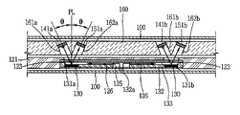
도 1 및 도 2를 참조하면, 본 발명의 일 실시예에 따른 물질 분석 장치는 키입력부(101)와 표시부(102)가 마련된 본체(100)와, 상기 본체(100)의 내부에 선택적으로 삽입되는 물질 분석용 칩(120)과, 광원(141)과, 광센서(151), 제어부(170) 및 메모리(180)를 포함한다.1 and 2, a material analyzing apparatus according to an embodiment of the present invention may be selectively inserted into a
상기 본체(100)는 물질 분석 장치의 외관을 형성하며, 상기 물질 분석용 칩(120)이 삽입될 수 있는 슬롯(103)이 일 측면에 형성된다. 상기 본체(100)의 정면에는 복수의 키가 마련된 키입력부(101)가 마련되며, 상기 키입력부(101)의 상부에는 산출된 데이터를 출력하기 위한 표시부(102)가 마련된다. 이러한 키입력부(101) 및 표시부(102)는 제어부(170)와 전기적으로 연결되어 있어서, 키입력부(101)로부터 입력된 신호는 제어부(170)로 전달될 수 있고, 제어부(170)로부터 출력된 신호는 상기 표시부(102)에 출력된다.The
상기 물질 분석용 칩(120)은 시료에 대한 분석을 할 수 있도록 시료가 투입된 상태로 상기 본체(100)의 내부에 삽입되며, 시료가 투입되기 전에는 사용자가 개별적으로 소지한다. 이러한 물질 분석용 칩(120)은, 도 3 및 도 4에 도시된 바와 같이, 칩 지지체(121)와, 칩 몸체(124)와, 제1 및 제2커버(132)(133)를 포함한다.The
상기 칩 지지체(121)는 일정한 강성을 가지는 수지제로 형성되어 상기 칩 몸체(124)를 지지 및 보호한다. 이러한 칩 지지체(121)에는 상기 칩 몸체(124)를 수 용하기 위한 수용부(122)가 마련되며, 상기 수용부(122)에는 복수의 광투과홀(123)이 형성된다. 상기 복수의 광투과홀(123)은, 도 4에 도시된 바와 같이, 상기 광원(141)으로부터 출사된 광을 상기 칩 몸체(124)에 도달할 수 있도록 통과시키며, 상기 칩 몸체(124)의 반응된 시료로부터 반사된 광을 상기 광센서(151)로 도달될 수 있도록 통과시킨다. 본 실시예에서는 별도의 칩 지지체(121)가 마련되는 것을 예시하였으나, 상기 칩 지지체(121)는 칩 몸체(124)가 일정 이상의 강성을 가지는 경우에는 생략될 수 있다.The
상기 칩 몸체(124)는 투입된 시료를 시약(130)과 반응시키기 위한 것으로서, 시료저장부(125), 시약저장부(131) 및 미세유로(126)가 형성된다.The
상기 시료저장부(125)는 시료가 투입되는 곳으로서, 칩 몸체(124)의 중앙부에 관통되어 형성된다.The
상기 시약저장부(131)는 복수개가 상기 시료저장부(125)의 주변에 방사상으로 배치되는 제1 내지 제4시약저장부(131a)(131b)(131c)(131d)를 포함하며, 상기 각 시약저장부(131a)(131b)(131c)(131d)는 상기 칩 몸체(124)를 관통하여 형성된다. 이러한 시약저장부(131a)(131b)(131c)(131d) 각각에는 시료내에 포함된 서로 다른 대상물질들 각각과 반응될 수 있도록 서로 다른 시약(130)이 마련된다. 일 예로, 혈액을 시료로 하는 경우에, 혈액내의 글루코오스(glucose)를 정량 정성분석하기 위해 글루코오스산화효소(glucose oxidase)와 페록시다아제(peroxidase)와 같은 효소와 MBTH(3-Methylbenzothiazolinone hydrazone)와 DMBA(7, 12-dimethylbenz[α]anthracene, 9, 10-dimethyl-1, 2-benzanthracene)와 같은 색소를 시약(130)으로 사용하며, 이와 같은 시약(130)과 글루코오스가 반응할 경우 상기 시약(130)은 파란색으로 변색되며, 글루코오스의 양(밀도)에 따라 파란색으로 변색되는 정도가 달라진다. 또한, 혈액내의 콜레스테롤(cholesterol)을 정량 정성분석하기 위해서는 콜레스테롤산화효소(cholesterol oxidase)와 페록시다아제(peroxidase) 및 콜레스테롤 에스테르가수분해효소(cholesterol esterase)와 같은 효소와 MBTH(3-Methylbenzothiazolinone hydrazone)와 DMBA(7, 12-dimethylbenz[α]anthracene, 9, 10-dimethyl-1, 2-benzanthracene)와 같은 색소를 시약(130)으로 사용하며, 이러한 시약(130)은 콜레스테롤과 반응하여 파란색으로 변색하며 콜레스테롤의 양에 따라 파란색으로 변색되는 정도가 달라진다. 이와 같이 혈액내의 각 대상물질과 반응하는 서로 다른 시약(130)을 제1 내지 제4 시약저장부(131a)(131b)(131c)(131d) 각각에 저장된다.The
상기 미세유로(126)는 상기 시료저장부(125)에 투입된 시료를 상기 각 시약저장부(131)로 이송시키기 위한 것으로서, 상기 시료저장부(125)와 상기 4개의 시약저장부(131a)(131b)(131c)(131d)를 각각 연결시킬 수 있도록 상기 칩 몸체(124)의 하면으로부터 상측으로 함몰되어 형성된다. 이와 같은 미세유로(126)는 상기 제2커버(133)에 의해 밀폐된다.The
이와 같은 구조를 가지는 칩 몸체(124)는 화학적, 생물학적으로 안정적인 탄성 중합체인 PDMS(Polydimethylsiloxane) 재질로 제작될 수 있으며, 상기 시료저장부(125)와 시약저장부(131) 및 미세유로(126)는 네거티브(negative) PR(Pohoto Resistor)을 이용한 소프트 리소그라피(soft lithography) 방법에 의해 형성될 수 있다. 한편, 상기 시료저장부(125)에 투입된 시료는 모세관 현상에 의해 상기 시약저장부(131)로 이송된다. 따라서, 상기 칩 몸체(124)에는 모세관 현상을 활성화시키기 위해 BSA(Bovine Serum Albumin) 등과 같은 친수성 물질이 코팅될 수 있다. 이와 같이 시료를 모세관 현상에 의해 시료저장부(125)로부터 시약저장부(131)로 이송함으로써, 마이크로 펌프과 같은 별도의 유체구동수단을 생략할 수 있게 되어 물질 분석용 칩(120)의 구조와 제조공정이 간소화될 수 있다. 또한, 물질 분석용 칩(120)의 두께를 줄일 수 있어 물질 분석용 칩(120)의 소형화에도 유리하다.The
상기 제1커버(132)는 상기 칩 몸체(124)의 상면을 덮도록 상기 칩 몸체(124)에 부착되며, 그 중앙에는 시료를 시료저장부(125)로 투입시키기 위한 투입구(132a)가 상기 시료저장부(125)에 대응하는 위치에 형성된다.The
상기 제2커버(133)는 상기 칩 몸체(124)의 하면에 부착되며, 상기 칩 몸체(124)와 협력하여 상기 미세유로(126)를 밀폐시킨다. 이러한 제1 및 제2커버(132)(133)는 광이 통과될 수 있도록 투명재질인 유리재질 등으로 제작된다.The
본 실시예에서는 상기 제1 및 제2커버(132)(133)를 통해 시료저장부(125)와 시약저장부(131) 및 미세유로(126)를 밀폐시키는 것을 예시하였으나, 칩 몸체(124)에 상기 시료저장부(125) 및 시약저장부(131)를 상기 미세유로(126)와 같이 일면으로부터 함몰되게 형성할 경우, 상기 제1 및 제2커버(132)(133) 중 어느 하나는 생략될 수 있다. 또한, 칩 몸체(124)를 증착공정 및 식각공정 등을 통해 시료저장부(125)와 시약저장부(131)와 미세유로(126) 및 투입구(132a)를 형성할 경우, 상기 제1 및 제2커버(132)(133)는 모두 생략될 수 있다.In the present exemplary embodiment, the
상기 광원(141)은, 도 2 및 도 4에 도시된 바와 같이, 상기 시약저장부(131)에서 시약(130)과 반응된 시료에 광을 조사하기 위한 것으로서, 각 시약저장부(131a)(131b)(131c)(131d)당 하나씩 배치된 제1 내지 제4광원(141a)(141b)(141c)(141d)을 포함한다. 상기 광원(141)은 상기 반응된 시료에 대해 일정 각도 경사지게 광을 조사한다. 이러한 광원(141)은 단일 파장의 광을 출사시키는 LED(Light Emitting Diode)나 LD(Laser Diode)가 이용될 수 있다. 본 실시예에서는 적색광을 출사시키는 LED(Light Emitting Diode)를 사용한다. 시료의 대상물질과 시약(130)과의 반응에 의해 시약(130)은 파란색으로 변색되므로, 상기 적색광이 상기 반응되어 파란색으로 변색된 시약에 조사될 경우, 파란색으로 변색된 정도에 따라서 상기 적색광이 반응된 시약(130)에 흡수되는 정도가 달라진다. 즉, 반응된 시료가 파란색으로 변색된 정도가 클수록 상기 시약(130)으로부터 반사된 광의 세기는 작아진다.As shown in FIGS. 2 and 4, the
상기 광센서(151)는 반응되어 변색된 시약(130)으로부터 반사된 광의 세기를 측정하기 위한 것으로서, 상기 광원(141)에 대응하는 수만큼 배치된 제 1 내지 제4광센서(151a)(151b)(151c)(151d)를 포함한다. 이러한 광센선(151)로는 포토 다이오드(Photo Diode)나 포토 트랜지스터(Photo Transistor)등이 이용될 수 있다. 상기 광센서(151)는 반사되는 광의 세기에 따라 전류의 값이 변동되고 이를 신호처리하여 제어부(170)로 출력한다.The
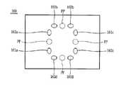
이러한 광원(141) 및 광센서(151)는 본체(100)의 내부에 형성된 지지리브(160)에 설치된다. 상기 지지리브(160)에는, 도 4 내지 도 5b에 도시된 바와 같 이, 광원용 홀(161)과 센서용 홀(162)이 형성되며, 상기 광원용 홀(161)의 내부에 상기 광원(141)이 설치되고, 상기 센서용 홀(162)에 상기 광센서(151)가 각각 설치된다. 상기 광원용 홀(161)은 칩 몸체(124)의 수직한 선에 대해 일방향으로 일정각도(θ) 경사지게 형성되고 상기 센서용 홀(162)은 칩 몸체(124)의 수직한 선에 대해 타방향으로 상기 광원용 홀(161)과 동일한 각도(θ)로 경사지게 형성된다. 이와 같이 광원용 홀(161)과 센서용 홀(162)을 마련하고, 각각의 내부에 광원(141)과 광센서(151)를 형성함으로써, 광원(141)으로부터 출사되어 반응된 시료에 입사되는 광과 반응된 시료로부터 반사되는 광의 간섭을 줄일 수 있다. 따라서, 광센서(151)에 의해 검출되는 광의 세기를 보다 정밀하게 측정할 수 있게 되고, 이에 의해 보다 정밀하게 시료를 정량 정성분석할 수 있게 된다.The
상술한 바와 같은 광원(141)과 광센서(151)는 각 시료저장부(125)마다 하나씩 한쌍으로 배치된다. 따라서, 4개의 시료저장부(125) 각각에 광을 조사할 수 있도록 제1 내지 제4광원(141a)(141b)(141c)(141d)과 상기 제1 내지 제4광원(141a)(141b)(141c)(141d)에 대응되게 제1 내지 제4광센서(151a)(151b)(151c)(151d)가 배치된다. 도 5a 및 도 5b는 광원용 홀(161a)(161b)(161c)(161d)과 센서용 홀(162a)(162b)(162c)(162d)이 지지리브(160)의 상면과 하면에 각각 배치된 상태를 나타낸 것이다. 도 5a 및 도 5b에 점선으로 표시된 부분(PP)은 시약저장부(131)의 위치를 지지리브(160) 상에 투영시킨 것으로서, 각 광원용 홀161a)(161b)(161c)(161d)과 각 센서용 홀(162a)(162b)(162c)(162d)은 각 시약저장부(131)에 수렴하는 형태로 경사진다.The
상기 제어부(170)는 상기 광센서(151)로부터 출력된 신호를 분석하여 시료내의 각 대상물질이 존재하는지 여부(정성) 및 얼마나 존재하는지 여부(정량)를 분석하여 표시부(102)로 출력한다. 보다 상세하게 설명하면, 메모리(180)에 기설정된 각 대상물질과 그 대상물질의 양에 따른 광의 세기가 설정되어 있고, 상기 제어부(170)는 상기 광센서(151)로부터 출력된 광의 세기를 메모리(180)의 기설정된 광의 세기와 비교하여 대상물질을 존재여부와 양을 분석하여 표시부(102)로 출력한다.The
이하에서는 이상의 구성을 가지는 본 발명의 일 실시예에 따른 물질 분석 장치의 동작에 대하여 설명한다.Hereinafter will be described the operation of the material analysis device according to an embodiment of the present invention having the above configuration.
도 4를 참조하면, 사용자는 인체로부터 시료인 혈액을 채취하여 물질 분석용 칩(120)의 투입구(132a)로 투입시킨다. 그러면, 투입된 혈액은 시약저장부(131)에 떨어지고, 모세관 현상에 의해 미세유로(126)를 따라 각 시약저장부(131a)(131b)(131c)(131d)로 균등한 양으로 분배되어 이송된다. 각 시약저장부(131a)(131b)(131c)(131d)로 이송된 혈액은 시약(130)과 반응한다. 이때, 혈액의 특정 대상물질은 시약(130)과 반응을 하여 대상물질의 양에 따라 시약(130)은 파란색으로 변색되는 정도가 달라진다. 따라서, 각 시약(130)이 파란색으로 발색되었는지 여부를 통해 특정 대상물질이 혈액속에 포함되어 있는지를 판단하고(정성분석), 파란색으로의 발색정도에 따라 혈액속에 얼마나 많은 양(밀도)이 포함되어 있는지를 판단한다(정량분석). 이하 이러한 판단을 하는 과정을 상세히 설명한다.Referring to FIG. 4, the user collects blood, which is a sample, from the human body and inserts the blood into the
광원(141)으로부터 적색광이 시약(130)과 반응된 시료에 입사된다. 이때, 대 상물질과 반응된 시약(130)이 파란색으로 변색된 정도에 따라 적색광을 흡수하는 정도가 달라진다. 즉, 파란색으로 변색된 정도가 높을 수록 반사되는 적색광은 그 세기가 줄어들게 된다. 따라서, 광센서(151)는 반응된 시약(130)으로부터 반사된 광의 세기를 측정하게 되고, 제어부(170)는 광의 세기가 높을수록 특정 대상물질의 양이 혈액속에 많이 포함되어 있다고 판단한다.Red light is incident on the sample reacted with the
상기 제어부(170)는 각 광센서(151)로부터 출력된 광의 세기에 대한 신호를 메모리(180)에 기설정된 광의 세기와 비교하여 특정 대상물질의 양을 산출하게 된다. 그리고, 산출된 각 대상물질의 양은 사용자가 인지할 수 있도록 표시부(102)로 출력된다. 특히, 특정 대상물질의 양이 정상의 범위에서 벗어난 경우, 제어부(170)는 경고의 메시지를 표시부(102)로 출력할 수 있다.The
또한, 상기 제어부(170)는 송수신장치(미 도시)를 통해 측정된 대상물질에 대한 정보를 개인의 병력이 관리될 수 있도록 병원이나 기타 의료기관등의 서버로 전송할 수도 있다.In addition, the
본 실시예에서는 반응된 시료의 발색정도를 측정하는 광학식을 사용하였으나, 시약저장부에 전압을 인가하고 시약과 대상물질의 반응정도에 따라 달라지는 전류의 양을 측정하여 대상물질의 정성 정량 분석하는 전기화학방식이 이용될 수도 있다.In the present embodiment, an optical formula for measuring the color development of the reacted sample was used, but applying a voltage to the reagent storage and measuring the amount of current that varies depending on the reaction degree of the reagent and the target material, the electric quantitative analysis of the target material was performed. Chemistry may also be used.
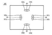
도 6a 내지 도 7은 본 발명의 다른 실시예에 따른 지지리브(260) 및 광원(241aa)(241ab)과 광센서(251a)를 개략적으로 나타낸 것으로서, 이를 참조하면 본 발명의 다른 실시예에 따른 광원(241aa, 241ab)은 하나의 시약저장부(231)에 서 로 다른 파장의 광의 조사할 수 있도록 서로 다른 파장의 광을 출사하는 제1 및 제2파장 광원(241aa)(241ab)을 포함한다.6A to 7 schematically illustrate the
상기 제1파장 광원(241aa)은 가시광선 영역의 제1파장의 광을 출사하여, 반응된 시약이 변색된 정도를 측정한다. 만약, 시약(130)과 반응한 시료가 파란색으로 변색되는 경우에는 제1파장의 광은 적색광인 650nm의 파장을 가지는 광인 것이 바람직하다.The first wavelength light source 241aa emits light of the first wavelength in the visible light region, and measures the degree of discoloration of the reacted reagent. If the sample reacted with the
상기 제2파장 광원(241ab)은 물질 분석용 칩(120, 도 1 참조)이 본체(100, 도 1 참조) 내부에 삽입된 상태에서 자세가 기울어지거나 시약저장부(231)의 표면의 오차로 인해 시약저장부(231)로부터 반사된 제1파장의 광 세기에 오류를 수정하기 위한 것으로서, 가시광선 영역 외의 영역의 파장인 것이 바람직하다. 이는 가시영역 이외의 파장을 가지는 광은 표면의 오차 등에 의해 반사광의 세기가 받는 영향이 작기 때문이다. 본 실시예에서는 제2파장의 광으로 적외선 영역의 광인 880nm 파장의 광을 사용된다.The second wavelength light source 241ab may be tilted in a state where the material analysis chip 120 (refer to FIG. 1) is inserted into the main body 100 (refer to FIG. 1) or due to an error of the surface of the
상기 광센서(251a)는 상기 제1 및 제2파장 광원(241aa)(241ab)으로부터 출사된 광이 시약저장부(231)로부터 반사되어 입사될 수 있는 위치에 마련된다. 즉, 상기 제1 및 제2파장 광원(241aa)(241ab)과 상기 광센서(251a) 및 시약저장부(231)를 연결하면, 정사면체를 이루도록 배치되는 것이 바람직하다.The
상술한 바와 같은 구성을 가지는 물질 분석 장치에 의하면, 제어부(170, 도 2 참조)는 시약저장부(231)의 반응된 시료로부터 반사된 제1파장의 광으로부터 광의 세기를 분석하고, 반응된 시료로부터 반사된 제2파장의 광으로부터 광의 세기를 분석하여 구조적인 오차를 측정하며, 측정된 오차를 반응된 시료의 정성 정량 분석에 반영하여 최종적으로 시료내 대상물질의 함유여부 및 함유된 양을 산출한다.According to the material analysis device having the above-described configuration, the control unit 170 (see FIG. 2) analyzes the light intensity from the light of the first wavelength reflected from the reacted sample of the
이와 같이 제1파장의 광으로 반응된 시료의 변색정도를 측정하고, 제2파장의 광으로부터 구조적인 오차를 수정함으로써, 대상물질을 더욱 정밀하게 정성 정량분석할 수 있다.Thus, by measuring the degree of discoloration of the sample reacted with the light of the first wavelength, and correcting the structural error from the light of the second wavelength, qualitative quantitative analysis of the target material can be more precise.
본 실시예에서는, 도 6a 및 도 6b에 도시된 바와 같이, 서로 다른 파장의 광을 각각 출사하는 제1 및 제2파장 광원(241aa)(241ab)은 두개의 시약저장부(231)에 대응하는 위치에 형성하고, 나머지 두개의 시약저장부는 본 발명의 일 실시예와 동일하게 하나의 광원을 사용하는 구조를 도시하였다. 즉, 도 6a 및 도 6b의 양측에는 위치하는 시약저장부에 대응하는 광원용 홀(261aa, 261ab)(261ca, 261cb)은 두개씩 형성되고, 센서용 홀(262a)(262c)은 하나씩 형성된다. 그러나, 상하로 위치하는 광원용 홀(261b)(261d)과 센서용 홀(262b)(261d)은 본 발명의 일 실시예와 동일하게 하나씩 형성된다. 이와 같은 구조로 보다 정밀한 분석이 필요한 대상물질을 정밀분석할 수 있게 된다. 여기서, 점선으로 표시된 부분은 시약저장부(231)를 각각 지지리브(260)에 투영한 위치(PP)를 나타낸다.6A and 6B, the first and second wavelength light sources 241aa and 241ab that emit light having different wavelengths respectively correspond to the two
도 8은 본 발명의 또 다른 실시예에 따른 칩 몸체(324)의 평면도를 도시한 것으로서, 이를 참조하면, 시료저장부(325)에 십자형 분배리브(338)가 형성된다. 이러한 분배리브(338)는 투입되는 시료를 각 시약저장부(331)에 균일량으로 분배하는 역활을 한다.8 illustrates a plan view of a
또한, 시료저장부(325)와 미세유로(326)의 연결부와, 미세유로(126)와 시약 저장부(131)의 연결부를 일정곡률을 가지는 곡면(R)을 가지도록 형성되므로서, 모세관 현상을 활성화시킬 수 있다.In addition, the capillary phenomenon is formed to have a connection portion of the
이와 같이 상기 분배리브(338)와 곡면(R)에 의해 시료를 보다 균일하고 신속하게 시약저장부(331)로 이송시킬 수 있게 되고, 이에 의해 보다 정밀하고 신속한 대상물질의 분석이 가능하다.As described above, the
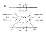
도 9는 본 발명의 또 다른 실시예에 따른 물질 분석용 칩(420)을 개략적으로 나타낸 평면도로서, 이에 도시된 바와 같이, 시약저장부(431)는 분석하고자 하는 대상물질의 개수에 대응되는 개수로 형성될 수 있다. 물론, 광원 및 광센서도 최소한 이와 동일한 개수로 배치되어야 함은 물론이다.9 is a plan view schematically showing a chip for analyzing a
상술한 바와 같은 본 발명의 실시예에 따른 물질 분석 장치는, 별도의 휴대용 물질분석기기 뿐만 아니라 물질분석기능이 구현된 PDA(Personal Digital[Data] Assistant )나 이동통신 단말기등과 같은 휴대용 전자기기를 포함한다.Material analysis apparatus according to an embodiment of the present invention as described above, not only a separate portable material analysis device, but also a portable electronic device such as a PDA (Personal Digital [Data] Assistant) or a mobile communication terminal implemented material analysis function Include.
이상에서 설명한 바와 같은 본 발명에 의하면, 시료저장부에 투입된 시료는 서로 다른 대상물질과 반응하는 서로 다른 시약이 마련된 복수의 시약저장부로 이송되고, 각 대상물질과 각 시약을 반응시켜 각 대상물질을 정량 정성분석함으로써, 한 번의 시료 투입으로 다양한 대상물질을 일시에 정량 정성분석할 수 있다.According to the present invention as described above, the sample introduced into the sample storage unit is transferred to a plurality of reagent storage units provided with different reagents reacting with different target substances, reacting each target substance with each reagent to react each target substance. By quantitative qualitative analysis, quantitative qualitative analysis of various target substances can be performed at one time with one sample input.
또한, 투입된 시료를 모세관 현상에 의해 시료저장부로부터 시약저장부로 이송시키므로써, 펌프와 같은 별도의 이송수단을 생략할 수 있어 부품수 및 제조비용을 줄일 뿐만 아니라 물질 분석용 칩의 크기를 줄일 수 있다.In addition, by transferring the injected sample from the sample storage unit to the reagent storage unit by capillary action, it is possible to omit a separate transfer means such as a pump to reduce the number of parts and manufacturing cost, as well as to reduce the size of the chip for material analysis. have.
또한, 광이 통과되는 홀을 형성함으로써, 광원으로부터 조사된 광과 반응된 시약(시료)로부터 반사된 광의 간섭현상을 방지할 수 있어 대상물질의 정밀한 정량 정성 분석이 가능하다.In addition, by forming a hole through which light passes, it is possible to prevent interference of light reflected from a reagent (sample) reacted with light irradiated from the light source, thereby enabling accurate quantitative qualitative analysis of the target material.
또한, 서로 다른 파장의 광을 이용하여 구조적인 오차를 보정함으로써, 대상물질을 더욱 정밀하게 정량 정성분석할 수 있다.In addition, by correcting the structural error using light of different wavelengths, it is possible to quantitatively analyze the target material more precisely.
또한, 분배리브를 시료저장부에 형성함으로써, 시료를 각 시약저장부에 균일하게 분배할 수 있다.In addition, by forming the distribution ribs in the sample reservoir, the sample can be uniformly distributed in each reagent reservoir.
또한, 시료저장부와 미세유로의 연결부 및 미세유로와 시약저장부의 연결부를 곡면으로 형성함으로써, 모세관 현상을 활성화시킬 수 있고 이에 의해 보다 신속하게 시료를 시약저장부에 이송시킬 수 있다. 따라서 시료의 대상물질을 보다 신속하게 정성 정량 분석할 수 있다.In addition, by forming the connection portion between the sample storage portion and the micro flow path and the connection portion between the micro flow path and the reagent storage portion, the capillary phenomenon can be activated, and thereby the sample can be transferred to the reagent storage portion more quickly. Therefore, qualitative quantitative analysis of the target material of the sample can be performed more quickly.
Claims (29)
Translated fromKoreanPriority Applications (1)
| Application Number | Priority Date | Filing Date | Title |
|---|---|---|---|
| KR1020060086240AKR100808415B1 (en) | 2006-09-07 | 2006-09-07 | Chip for material analysis and material analysis device including the same |
Applications Claiming Priority (1)
| Application Number | Priority Date | Filing Date | Title |
|---|---|---|---|
| KR1020060086240AKR100808415B1 (en) | 2006-09-07 | 2006-09-07 | Chip for material analysis and material analysis device including the same |
Publications (1)
| Publication Number | Publication Date |
|---|---|
| KR100808415B1true KR100808415B1 (en) | 2008-02-29 |
Family
ID=39383625
Family Applications (1)
| Application Number | Title | Priority Date | Filing Date |
|---|---|---|---|
| KR1020060086240AExpired - Fee RelatedKR100808415B1 (en) | 2006-09-07 | 2006-09-07 | Chip for material analysis and material analysis device including the same |
Country Status (1)
| Country | Link |
|---|---|
| KR (1) | KR100808415B1 (en) |
Cited By (11)
| Publication number | Priority date | Publication date | Assignee | Title |
|---|---|---|---|---|
| KR100961850B1 (en)* | 2008-10-30 | 2010-06-09 | 주식회사 올메디쿠스 | Powerless Microfluidic Chips Using Hydrophilic Films |
| KR101152642B1 (en) | 2010-10-28 | 2012-06-07 | 한국과학기술연구원 | Method of preparing microfluidic devices based on a polymer |
| KR101380368B1 (en) | 2012-09-18 | 2014-04-10 | 포항공과대학교 산학협력단 | Microfluidic chips having flow cells for absorbance measurements and absorbance measurement apparatus having thereof |
| WO2015005504A1 (en)* | 2013-07-08 | 2015-01-15 | 가천대학교 산학협력단 | Biochip for measuring blood glucose levels, and blood glucose meter for smartphone, containing same |
| WO2015137694A1 (en)* | 2014-03-11 | 2015-09-17 | 포항공과대학교 산학협력단 | Microfluidic chip having flow cell, and using standard addition method, and absorbance detection apparatus comprising same |
| WO2015137753A1 (en)* | 2014-03-13 | 2015-09-17 | 포항공과대학교 산학협력단 | Continuous microfluidic apparatus for analyzing total nitrogen and total phosphorus |
| KR102002057B1 (en)* | 2018-08-30 | 2019-07-19 | 가천대학교 산학협력단 | Isothermal amplification microdevice for detection of pathogens and method the same |
| KR20200120832A (en)* | 2019-04-12 | 2020-10-22 | 가천대학교 산학협력단 | Foldable typed isothermal amplification microdevice for detection of pathogens and method the same |
| WO2021107398A1 (en)* | 2019-11-29 | 2021-06-03 | 양태양 | Optical protein measurement sensor |
| KR20210120178A (en)* | 2020-03-25 | 2021-10-07 | 성균관대학교산학협력단 | 3 dimensional microfluidic analytical device and making method thereby |
| KR20230111820A (en)* | 2022-01-19 | 2023-07-26 | 계명대학교 산학협력단 | Lactate fluorescence measurement method and Fluorescence analyzer for simultaneous measurement of glucose and lactate |
Citations (5)
| Publication number | Priority date | Publication date | Assignee | Title |
|---|---|---|---|---|
| JPH08114539A (en)* | 1994-08-25 | 1996-05-07 | Nihon Medi Physics Co Ltd | Body fluid component analysis instrument and analysis method |
| KR20040013003A (en)* | 2001-06-29 | 2004-02-11 | 인터내셔널 비지네스 머신즈 코포레이션 | Measurement testing of blood specimens |
| US20040129678A1 (en)* | 2002-09-07 | 2004-07-08 | Timothy Crowley | Integrated apparatus and methods for treating liquids |
| WO2004065930A2 (en) | 2003-01-14 | 2004-08-05 | Micronics Inc. | Microfluidic devices for fluid manipulation and analysis |
| KR20060064807A (en)* | 2004-12-09 | 2006-06-14 | 주식회사 바이오디지트 | Lab Detectors for Field Analysis and Signal Detectors for Lab-on-A-Chips |
- 2006
- 2006-09-07KRKR1020060086240Apatent/KR100808415B1/ennot_activeExpired - Fee Related
Patent Citations (5)
| Publication number | Priority date | Publication date | Assignee | Title |
|---|---|---|---|---|
| JPH08114539A (en)* | 1994-08-25 | 1996-05-07 | Nihon Medi Physics Co Ltd | Body fluid component analysis instrument and analysis method |
| KR20040013003A (en)* | 2001-06-29 | 2004-02-11 | 인터내셔널 비지네스 머신즈 코포레이션 | Measurement testing of blood specimens |
| US20040129678A1 (en)* | 2002-09-07 | 2004-07-08 | Timothy Crowley | Integrated apparatus and methods for treating liquids |
| WO2004065930A2 (en) | 2003-01-14 | 2004-08-05 | Micronics Inc. | Microfluidic devices for fluid manipulation and analysis |
| KR20060064807A (en)* | 2004-12-09 | 2006-06-14 | 주식회사 바이오디지트 | Lab Detectors for Field Analysis and Signal Detectors for Lab-on-A-Chips |
Cited By (16)
| Publication number | Priority date | Publication date | Assignee | Title |
|---|---|---|---|---|
| KR100961850B1 (en)* | 2008-10-30 | 2010-06-09 | 주식회사 올메디쿠스 | Powerless Microfluidic Chips Using Hydrophilic Films |
| KR101152642B1 (en) | 2010-10-28 | 2012-06-07 | 한국과학기술연구원 | Method of preparing microfluidic devices based on a polymer |
| KR101380368B1 (en) | 2012-09-18 | 2014-04-10 | 포항공과대학교 산학협력단 | Microfluidic chips having flow cells for absorbance measurements and absorbance measurement apparatus having thereof |
| WO2015005504A1 (en)* | 2013-07-08 | 2015-01-15 | 가천대학교 산학협력단 | Biochip for measuring blood glucose levels, and blood glucose meter for smartphone, containing same |
| US10732119B2 (en) | 2013-07-08 | 2020-08-04 | Gachon University Industry Academic Cooperation Foundation | Biochip for measuring blood glucose levels, and blood glucose meter for smartphone, containing same |
| WO2015137694A1 (en)* | 2014-03-11 | 2015-09-17 | 포항공과대학교 산학협력단 | Microfluidic chip having flow cell, and using standard addition method, and absorbance detection apparatus comprising same |
| WO2015137753A1 (en)* | 2014-03-13 | 2015-09-17 | 포항공과대학교 산학협력단 | Continuous microfluidic apparatus for analyzing total nitrogen and total phosphorus |
| KR102002057B1 (en)* | 2018-08-30 | 2019-07-19 | 가천대학교 산학협력단 | Isothermal amplification microdevice for detection of pathogens and method the same |
| KR20200120832A (en)* | 2019-04-12 | 2020-10-22 | 가천대학교 산학협력단 | Foldable typed isothermal amplification microdevice for detection of pathogens and method the same |
| KR102221289B1 (en) | 2019-04-12 | 2021-03-02 | 가천대학교 산학협력단 | Foldable typed isothermal amplification microdevice for detection of pathogens and method the same |
| WO2021107398A1 (en)* | 2019-11-29 | 2021-06-03 | 양태양 | Optical protein measurement sensor |
| KR20210120178A (en)* | 2020-03-25 | 2021-10-07 | 성균관대학교산학협력단 | 3 dimensional microfluidic analytical device and making method thereby |
| KR102400288B1 (en) | 2020-03-25 | 2022-05-23 | 성균관대학교산학협력단 | 3 dimensional microfluidic analytical device and making method thereby |
| KR20230111820A (en)* | 2022-01-19 | 2023-07-26 | 계명대학교 산학협력단 | Lactate fluorescence measurement method and Fluorescence analyzer for simultaneous measurement of glucose and lactate |
| WO2023140613A1 (en)* | 2022-01-19 | 2023-07-27 | 계명대학교 산학협력단 | Lactate fluorescence measurement method and fluorometric assay substrate for simultaneous measurement of glucose and lactate |
| KR102705833B1 (en) | 2022-01-19 | 2024-09-11 | 계명대학교 산학협력단 | Fluorescence analyzer for simultaneous measurement of glucose and lactate |
Similar Documents
| Publication | Publication Date | Title |
|---|---|---|
| KR100808415B1 (en) | Chip for material analysis and material analysis device including the same | |
| AU2019216581B2 (en) | A microfluidic detection system and a microfluidic cartridge | |
| JP5203453B2 (en) | Reaction vessel with integrated optical and fluid control elements | |
| US20220283191A1 (en) | Optical reader for analyte testing | |
| EP1921439B1 (en) | Measuring device, measuring instrument and method of measuring | |
| US20180128715A1 (en) | Station, used for test apparatus, having integrated reaction and detection means | |
| US20130095508A1 (en) | Instrumented pipette | |
| US11067526B2 (en) | Devices, systems, and methods for performing optical and electrochemical assays | |
| US11060994B2 (en) | Techniques for performing optical and electrochemical assays with universal circuitry | |
| US11253852B2 (en) | Devices, systems, and methods for performing optical assays | |
| US20250130170A1 (en) | Optical analyte detection | |
| EP2990779A1 (en) | Device for detecting analyzed object in specimen and method therefor | |
| JP4985646B2 (en) | Reaction vessel kit | |
| US20150014162A1 (en) | Connector for connecting bio-sensor and measuring instrument thereof | |
| KR20130032461A (en) | Biosensor and measuring apparatus therefor | |
| US20180195967A1 (en) | Test instrument and method of controlling the same | |
| JP4591407B2 (en) | Reaction kit | |
| JP2007285834A (en) | Reaction vessel |
Legal Events
| Date | Code | Title | Description |
|---|---|---|---|
| A201 | Request for examination | ||
| PA0109 | Patent application | St.27 status event code:A-0-1-A10-A12-nap-PA0109 | |
| PA0201 | Request for examination | St.27 status event code:A-1-2-D10-D11-exm-PA0201 | |
| D13-X000 | Search requested | St.27 status event code:A-1-2-D10-D13-srh-X000 | |
| D14-X000 | Search report completed | St.27 status event code:A-1-2-D10-D14-srh-X000 | |
| E902 | Notification of reason for refusal | ||
| PE0902 | Notice of grounds for rejection | St.27 status event code:A-1-2-D10-D21-exm-PE0902 | |
| E13-X000 | Pre-grant limitation requested | St.27 status event code:A-2-3-E10-E13-lim-X000 | |
| P11-X000 | Amendment of application requested | St.27 status event code:A-2-2-P10-P11-nap-X000 | |
| P13-X000 | Application amended | St.27 status event code:A-2-2-P10-P13-nap-X000 | |
| E701 | Decision to grant or registration of patent right | ||
| PE0701 | Decision of registration | St.27 status event code:A-1-2-D10-D22-exm-PE0701 | |
| GRNT | Written decision to grant | ||
| PR0701 | Registration of establishment | St.27 status event code:A-2-4-F10-F11-exm-PR0701 | |
| PR1002 | Payment of registration fee | St.27 status event code:A-2-2-U10-U11-oth-PR1002 Fee payment year number:1 | |
| PG1601 | Publication of registration | St.27 status event code:A-4-4-Q10-Q13-nap-PG1601 | |
| G170 | Re-publication after modification of scope of protection [patent] | ||
| PG1701 | Publication of correction | St.27 status event code:A-5-5-P10-P19-oth-PG1701 Patent document republication publication date:20080410 Republication note text:Request for Correction Notice (Document Request) Gazette number:1008084150000 Gazette reference publication date:20080229 | |
| PN2301 | Change of applicant | St.27 status event code:A-5-5-R10-R13-asn-PN2301 St.27 status event code:A-5-5-R10-R11-asn-PN2301 | |
| R18-X000 | Changes to party contact information recorded | St.27 status event code:A-5-5-R10-R18-oth-X000 | |
| R18-X000 | Changes to party contact information recorded | St.27 status event code:A-5-5-R10-R18-oth-X000 | |
| FPAY | Annual fee payment | Payment date:20101223 Year of fee payment:4 | |
| PR1001 | Payment of annual fee | St.27 status event code:A-4-4-U10-U11-oth-PR1001 Fee payment year number:4 | |
| LAPS | Lapse due to unpaid annual fee | ||
| PC1903 | Unpaid annual fee | St.27 status event code:A-4-4-U10-U13-oth-PC1903 Not in force date:20120223 Payment event data comment text:Termination Category : DEFAULT_OF_REGISTRATION_FEE | |
| PC1903 | Unpaid annual fee | St.27 status event code:N-4-6-H10-H13-oth-PC1903 Ip right cessation event data comment text:Termination Category : DEFAULT_OF_REGISTRATION_FEE Not in force date:20120223 | |
| PN2301 | Change of applicant | St.27 status event code:A-5-5-R10-R13-asn-PN2301 St.27 status event code:A-5-5-R10-R11-asn-PN2301 | |
| P22-X000 | Classification modified | St.27 status event code:A-4-4-P10-P22-nap-X000 | |
| PN2301 | Change of applicant | St.27 status event code:A-5-5-R10-R13-asn-PN2301 St.27 status event code:A-5-5-R10-R11-asn-PN2301 |