KR100808056B1 - Pattern formation method using hard mask - Google Patents
Pattern formation method using hard maskDownload PDFInfo
- Publication number
- KR100808056B1 KR100808056B1KR1020060134340AKR20060134340AKR100808056B1KR 100808056 B1KR100808056 B1KR 100808056B1KR 1020060134340 AKR1020060134340 AKR 1020060134340AKR 20060134340 AKR20060134340 AKR 20060134340AKR 100808056 B1KR100808056 B1KR 100808056B1
- Authority
- KR
- South Korea
- Prior art keywords
- layer
- hard mask
- tungsten film
- forming
- pattern
- Prior art date
- Legal status (The legal status is an assumption and is not a legal conclusion. Google has not performed a legal analysis and makes no representation as to the accuracy of the status listed.)
- Expired - Fee Related
Links
Images


Classifications
- H—ELECTRICITY
- H01—ELECTRIC ELEMENTS
- H01L—SEMICONDUCTOR DEVICES NOT COVERED BY CLASS H10
- H01L21/00—Processes or apparatus adapted for the manufacture or treatment of semiconductor or solid state devices or of parts thereof
- H01L21/02—Manufacture or treatment of semiconductor devices or of parts thereof
- H01L21/027—Making masks on semiconductor bodies for further photolithographic processing not provided for in group H01L21/18 or H01L21/34
- H01L21/033—Making masks on semiconductor bodies for further photolithographic processing not provided for in group H01L21/18 or H01L21/34 comprising inorganic layers
- H01L21/0332—Making masks on semiconductor bodies for further photolithographic processing not provided for in group H01L21/18 or H01L21/34 comprising inorganic layers characterised by their composition, e.g. multilayer masks, materials
- H—ELECTRICITY
- H01—ELECTRIC ELEMENTS
- H01L—SEMICONDUCTOR DEVICES NOT COVERED BY CLASS H10
- H01L21/00—Processes or apparatus adapted for the manufacture or treatment of semiconductor or solid state devices or of parts thereof
- H01L21/02—Manufacture or treatment of semiconductor devices or of parts thereof
- H01L21/04—Manufacture or treatment of semiconductor devices or of parts thereof the devices having potential barriers, e.g. a PN junction, depletion layer or carrier concentration layer
- H01L21/18—Manufacture or treatment of semiconductor devices or of parts thereof the devices having potential barriers, e.g. a PN junction, depletion layer or carrier concentration layer the devices having semiconductor bodies comprising elements of Group IV of the Periodic Table or AIIIBV compounds with or without impurities, e.g. doping materials
- H01L21/30—Treatment of semiconductor bodies using processes or apparatus not provided for in groups H01L21/20 - H01L21/26
- H01L21/302—Treatment of semiconductor bodies using processes or apparatus not provided for in groups H01L21/20 - H01L21/26 to change their surface-physical characteristics or shape, e.g. etching, polishing, cutting
- H01L21/306—Chemical or electrical treatment, e.g. electrolytic etching
- H01L21/308—Chemical or electrical treatment, e.g. electrolytic etching using masks
- H01L21/3081—Chemical or electrical treatment, e.g. electrolytic etching using masks characterised by their composition, e.g. multilayer masks, materials
- H—ELECTRICITY
- H01—ELECTRIC ELEMENTS
- H01L—SEMICONDUCTOR DEVICES NOT COVERED BY CLASS H10
- H01L21/00—Processes or apparatus adapted for the manufacture or treatment of semiconductor or solid state devices or of parts thereof
- H01L21/02—Manufacture or treatment of semiconductor devices or of parts thereof
- H01L21/04—Manufacture or treatment of semiconductor devices or of parts thereof the devices having potential barriers, e.g. a PN junction, depletion layer or carrier concentration layer
- H01L21/18—Manufacture or treatment of semiconductor devices or of parts thereof the devices having potential barriers, e.g. a PN junction, depletion layer or carrier concentration layer the devices having semiconductor bodies comprising elements of Group IV of the Periodic Table or AIIIBV compounds with or without impurities, e.g. doping materials
- H01L21/30—Treatment of semiconductor bodies using processes or apparatus not provided for in groups H01L21/20 - H01L21/26
- H01L21/31—Treatment of semiconductor bodies using processes or apparatus not provided for in groups H01L21/20 - H01L21/26 to form insulating layers thereon, e.g. for masking or by using photolithographic techniques; After treatment of these layers; Selection of materials for these layers
- H01L21/3105—After-treatment
- H01L21/311—Etching the insulating layers by chemical or physical means
- H01L21/31105—Etching inorganic layers
- H01L21/31111—Etching inorganic layers by chemical means
- H01L21/31116—Etching inorganic layers by chemical means by dry-etching
- H—ELECTRICITY
- H01—ELECTRIC ELEMENTS
- H01L—SEMICONDUCTOR DEVICES NOT COVERED BY CLASS H10
- H01L21/00—Processes or apparatus adapted for the manufacture or treatment of semiconductor or solid state devices or of parts thereof
- H01L21/02—Manufacture or treatment of semiconductor devices or of parts thereof
- H01L21/04—Manufacture or treatment of semiconductor devices or of parts thereof the devices having potential barriers, e.g. a PN junction, depletion layer or carrier concentration layer
- H01L21/18—Manufacture or treatment of semiconductor devices or of parts thereof the devices having potential barriers, e.g. a PN junction, depletion layer or carrier concentration layer the devices having semiconductor bodies comprising elements of Group IV of the Periodic Table or AIIIBV compounds with or without impurities, e.g. doping materials
- H01L21/30—Treatment of semiconductor bodies using processes or apparatus not provided for in groups H01L21/20 - H01L21/26
- H01L21/31—Treatment of semiconductor bodies using processes or apparatus not provided for in groups H01L21/20 - H01L21/26 to form insulating layers thereon, e.g. for masking or by using photolithographic techniques; After treatment of these layers; Selection of materials for these layers
- H01L21/3205—Deposition of non-insulating-, e.g. conductive- or resistive-, layers on insulating layers; After-treatment of these layers
- H01L21/321—After treatment
- H01L21/3213—Physical or chemical etching of the layers, e.g. to produce a patterned layer from a pre-deposited extensive layer
- H01L21/32139—Physical or chemical etching of the layers, e.g. to produce a patterned layer from a pre-deposited extensive layer using masks
Landscapes
- Engineering & Computer Science (AREA)
- Microelectronics & Electronic Packaging (AREA)
- Condensed Matter Physics & Semiconductors (AREA)
- General Physics & Mathematics (AREA)
- Manufacturing & Machinery (AREA)
- Computer Hardware Design (AREA)
- Physics & Mathematics (AREA)
- Power Engineering (AREA)
- Chemical & Material Sciences (AREA)
- Inorganic Chemistry (AREA)
- Chemical Kinetics & Catalysis (AREA)
- General Chemical & Material Sciences (AREA)
- Internal Circuitry In Semiconductor Integrated Circuit Devices (AREA)
- Drying Of Semiconductors (AREA)
Abstract
Translated fromKoreanDescription
Translated fromKorean도 1은 종래기술에 따른 패턴 형성 방법을 도시한 도면.1 is a view showing a pattern forming method according to the prior art.
도 2는 패턴을 형성한 후에 발생된 이물질을 보여주는 도면.2 is a view showing foreign matter generated after forming a pattern.
도 3a 내지 도 3c는 본 발명의 실시예에 따른 하드마스크 제조 방법을 도시한 도면.3a to 3c illustrate a hard mask manufacturing method according to an embodiment of the present invention.
도 4a는 표면처리에 의한 변형층의 표면 두께별 변형 정도를 비교한 도면.Figure 4a is a view comparing the degree of deformation for each surface thickness of the strained layer by the surface treatment.
도 4b는 텅스텐막 표면에 변형층이 형성된 상태를 나타낸 사진.4B is a photograph showing a state in which a strained layer is formed on a surface of a tungsten film.
도 5는 본 발명의 실시예에 따른 하드마스크를 이용한 패턴 형성 방법을 도시한 공정 단면도.Figure 5 is a cross-sectional view showing a pattern forming method using a hard mask according to an embodiment of the present invention.
* 도면의 주요 부분에 대한 부호의 설명* Explanation of symbols for the main parts of the drawings
21 : 하부층21: lower layer
22 : 변형층22: strained layer
23 : 상부층23: top layer
100 : 표면처리100: surface treatment
본 발명은 반도체소자의 제조 방법에 관한 것으로, 특히 하드마스크 제조 방법 및 그를 이용한 패턴 형성 방법에 관한 것이다.The present invention relates to a method of manufacturing a semiconductor device, and more particularly, to a hard mask manufacturing method and a pattern forming method using the same.
반도체소자가 축소(Shrink)됨에 따라 게이트라인, 비트라인 등의 라인패턴(Line Pattern)의 경우, 식각 중 감광막마진(PR Margin)과 이후 홀 정의(Hole Define) 시의 자기정렬콘택마진(Self Aligned Contact Margin) 부족으로 다층의 하드마스크(Hard Mask) 구조를 이용한다.As the semiconductor device shrinks, in the case of a line pattern such as a gate line or a bit line, a PR Margin during etching and a self-aligned contact margin during subsequent hole definition are performed. Due to lack of contact margin, a multilayer hard mask structure is used.
도 1은 종래기술에 따른 패턴 형성 방법을 도시한 도면이다.1 is a view showing a pattern forming method according to the prior art.
도 1을 참조하여 패턴 형성 방법을 살펴보면, 피식각층(11)을 형성한 후, 다층의 하드마스크(12)를 형성한다. 이때, 하드마스크(12)는 적어도 하부층(12A)과 상부층(12B)의 순서로 적층된 다층 구조이며, 하부층(12A)과 상부층(12B)은 서로 다른 물질이다.Referring to FIG. 1, a pattern forming method is described. After forming the
이어서, 하드마스크(12) 상에 노광공정시 난반사를 방지하기 위한 반사방지막으로서 BARC(Bottom Anti Reflective Coating layer, 13)를 형성한 후, 감광막패턴(14)을 형성한다.Subsequently, a BARC (Bottom Anti Reflective Coating layer) 13 is formed on the
이후, 감광막패턴(14)을 식각장벽으로 하여 BARC(13)를 식각하고, 연속해서하드마스크(12)와 피식각층(11)을 식각하여 패턴을 완성한다.Thereafter, the BARC 13 is etched using the
그러나, 종래기술의 다층 하드마스크(12)는 하부층(12A)과 상부층(12B)간 층 간 부조화 현상으로 패턴 형성 후 일부 패턴에서 이상 현상이 발생하게 된다. 특히, 다층 하드마스크(12)가 텅스텐막과 비정질카본을 포함하는 경우, 텅스텐막과 비정질카본이 직접 접촉하는 경우에는 이물질이 다량 발생하는 문제가 있다.However, the multi-layered
도 2는 패턴을 형성한 후에 발생된 이물질을 보여주는 도면이다.2 is a view showing a foreign matter generated after the pattern is formed.
도 2와 같은 이물질은 다층 하드마스크 중의 텅스텐막과 비정질카본간의 비정상적인 불균일 접촉에 의해 식각 공정시 발생하는 것으로서, 텅스텐막(W) 표면에 발생된다. 이러한 이물질은 텅스텐 또는 비정질카본 중 어느 하나의 막을 생략할 경우에는 발생하지 않는다.The foreign matter as shown in FIG. 2 is generated during the etching process due to abnormal non-uniform contact between the tungsten film and the amorphous carbon in the multilayer hard mask, and is generated on the surface of the tungsten film (W). Such foreign matter does not occur when the film of either tungsten or amorphous carbon is omitted.
그러나, 텅스텐막과 비정질카본의 두 개의 막을 하드마스크로 사용하는 이유는 패턴 형성과 이후 콘택홀 등의 자기정렬콘택 식각 공정시의 자기정렬콘택 마진을 증가시키기 위하여 사용하는 것으로 이를 생략할 수는 없다.However, the reason for using two layers of tungsten film and amorphous carbon as a hard mask is to increase the self-aligned contact margin during pattern formation and subsequent self-aligned contact etching process such as contact hole, which cannot be omitted. .
본 발명은 상기한 종래기술의 문제점을 해결하기 위해 제안된 것으로서, 다층의 하드마스크 사용시 이물질 생성을 방지함과 동시에 자기정렬콘택마진을 증가시킬 수 있는 하드마스크를 이용한 패턴 형성 방법을 제공하는데 그 목적이 있다.The present invention has been proposed to solve the problems of the prior art, to provide a pattern forming method using a hard mask that can increase the self-aligned contact margin while preventing the generation of foreign substances when using a multi-layer hard mask. There is this.
상기 목적을 달성하기 위한 본 발명의 패턴 형성 방법은 피식각층을 형성하는 단계; 상기 피식각층 상에 텅스텐막과 비정질카본 사이에 상기 텅스텐막의 일부를 변형시킨 변형층이 삽입된 다층의 하드마스크를 형성하는 단계; 상기 하드마스크를 식각하는 단계; 및 상기 피식각층을 식각하는 단계를 포함하는 것을 특징으로 한다.Pattern forming method of the present invention for achieving the above object comprises the steps of forming an etched layer; Forming a multi-layer hard mask on the etched layer, wherein a strained layer in which a part of the tungsten film is deformed is inserted between the tungsten film and the amorphous carbon; Etching the hard mask; And etching the etched layer.
이하, 본 발명이 속하는 기술분야에서 통상의 지식을 가진 자가 본 발명의 기술적 사상을 용이하게 실시할 수 있을 정도로 상세히 설명하기 위하여, 본 발명의 가장 바람직한 실시예를 첨부 도면을 참조하여 설명하기로 한다.Hereinafter, the preferred embodiments of the present invention will be described in detail with reference to the accompanying drawings so that those skilled in the art may easily implement the technical idea of the present invention. .
후술하는 실시예는, 다층의 하드마스크에서 층간의 부조화를 해소하고 균일한 식각으로 안정적인 패턴을 형성하고자 하며, 이를 위해 다층 하드마스크 공정 중간에 일정 두께의 표면 처리를 통해 하부층과 상부층간 불균일을 해소하여 불필요한 이물질의 생성을 억제하고자 한다.The embodiments described below are intended to solve the inconsistency between the layers in the multi-layer hard mask and to form a stable pattern with uniform etching. For this purpose, the non-uniformity between the lower layer and the upper layer is eliminated through a surface treatment of a certain thickness in the middle of the multi-layer hard mask process. This is to suppress the generation of unnecessary foreign matter.
도 3a 내지 도 3c는 본 발명의 실시예에 따른 하드마스크 제조 방법을 도시한 도면이다.3A to 3C are diagrams illustrating a hard mask manufacturing method according to an exemplary embodiment of the present invention.
도 3a에 도시된 바와 같이, 하부층(Bottom Hard Mask, 21)을 형성한다. 여기서, 하부층(21)은 질화막(Nitride, 21A)과 텅스텐막(W, 21B)을 적층한 구조이다.As shown in FIG. 3A, a bottom
도 3b에 도시된 바와 같이, 표면처리(100)를 진행하여 하부층(21)의 표면에 일정 깊이의 변형층(22)을 형성한다. 이때, 변형층(22)은 하부층(21) 중 텅스텐막(21B)이 일부 변형된 것이다.As shown in FIG. 3B, the
도 3c에 도시된 바와 같이, 변형층(22)이 형성된 하부층(21) 상에 상부층(Top Hard Mask, 23)을 형성한다. 여기서, 상부층(23)은 비정질카본(ACL)일 수 있고, 비정질카본(ACL)과 SiON이 적층된 구조일 수도 있다.As shown in FIG. 3C, a top
도 3b에서 변형층(22) 형성을 위한 방법은 다음과 같다.In FIG. 3B, the method for forming the
표면처리(100)는 비소(As), 인(Phosphorous, P) 또는 보론(Boron, B)과 같은 불순물을 함유한 가스를 이용한 이온주입법(Implant)을 이용하거나 또는 글로우방전(Glow discharge) 또는 플라즈마파워(Plasma power)를 이용하여 이온화시킨 입자를 표면에 입사시키는 플라즈마도핑법(Plasma Doping, PLAD)을 이용한다. 예를 들어, 표면처리(100)를 위한 불순물 함유 가스는 PH3, AsH3, B2H6 또는 BF3 가스 중에서 선택된 어느 하나를 이용하며, 사용하는 에너지는 적어도 3KeV 이상이다. 한편, 플라즈마도핑법 사용시에는 아르곤(Ar) 가스를 첨가가스로 사용할 수 있다.The
이와 같은 표면처리(100)를 통해 텅스텐막(21B) 표면 내에 비소(As), 인(P) 또는 보론(B)이 축적된 변형층(22)을 형성하게 된다. 즉, 변형층(22)은 불순물이 함유된 텅스텐막, 예컨대, 비소가 함유된 텅스텐막(As containing W), 인이 함유된 텅스텐막(P containing W) 또는 보론이 함유된 텅스텐막(B containing W)이 된다.Through the
도 4a는 표면처리에 의한 변형층의 표면 두께별 변형 정도를 비교한 도면이다. 도 4a의 결과는 보론(B)을 이온주입법 또는 플라즈마도핑법을 이용하여 주입한 경우로서, 이온주입법에 의한 보론의 주입은 5KeV의 이온주입에너지와 1.6×10¹⁶atoms/cm2의 도즈량으로 진행하고, 플라즈마도핑법에 의한 보론의 주입은 도즈량을 2×10¹⁶atoms/cm2으로 하되 이온주입에너지를 7KV, 8KV, 9KV로 스플릿하여 진행한 결과이다. 바람직하게, 변형층(22)은 표면에서 200∼400Å까지의 텅스텐 막(21B)를 일부 변형시키게 된다.Figure 4a is a view comparing the degree of deformation for each surface thickness of the strained layer by the surface treatment. The results of FIG. 4A show that boron B was implanted by ion implantation or plasma doping. The boron implantation by ion implantation was performed using ion implantation energy of 5 KeV and dose of 1.6 × 10¹⁶ atoms / cm2 . The boron injection by the plasma doping method was performed by splitting the dose amount to 2 × 10¹⁶ atoms / cm2 , but splitting the ion implantation energy into 7KV, 8KV, and 9KV. Preferably, the
도 4a의 결과로부터 알 수 있듯이, 변형층(22)이 텅스텐막 내부로 어느 정도의 깊이에 어느 정도의 보론 농도 분포를 갖고 형성되는지를 알 수 있다. 즉, 표면으로부터 원하는 깊이까지 텅스텐막(21B)의 일정 부분의 성질을 변형시킨다.As can be seen from the result of FIG. 4A, it can be seen that the
또한, 일정 두께의 성질 변형을 통해 텅스텐막(21B) 표면 상부로 변형층(22)이 적층되는 적층 현상이 발생하는데, 변형층(22)의 종류는 사용하는 이온의 종류에 따라 달라지게 된다.In addition, a lamination phenomenon occurs in which the
도 4b는 텅스텐막 표면에 변형층이 형성된 상태를 나타낸 사진으로서, 변형층(22)이 텅스텐막(21B) 위에 적층됨을 알 수 있다. 그리고, 변형층(22) 위에는 비정질카본(ACL)이 형성된다.4B is a photograph showing a state in which the strained layer is formed on the surface of the tungsten film, and it can be seen that the
전술한 바와 같은 표면처리를 통해 형성되는 변형층(22)에 의해 텅스텐막(21B)과 상부층(23), 특히 비정질카본(ACL)과 텅스텐막(21B)간 직접적인 접촉을 방지하여 두 막간 비정상적인 결합에 의한 이물질의 생성을 억제한다. 결국, 변형층(22)은 하부층(21)과 상부층(23)간의 버퍼(Buffer) 역할을 수행하게 된다.The
그리고, 본 발명의 하드마스크는 하부층(21), 변형층(22) 및 상부층(23)의 순서로 적층된 다층 구조가 된다. 바람직하게는, 질화막(21A), 텅스텐막(21B), 변형층(22) 및 비정질카본(ACL)의 순서로 적층된 구조 또는 질화막(21A), 텅스텐막(21B), 변형층(22), 비정질카본(ACL) 및 SiON의 순서로 적층된 구조가 된다. 이러한 다층구조의 하드마스크는 홀 형성을 위한 자기정렬콘택 식각공정시 자기정렬콘택 마진을 증가시키는 역할을 충분히 수행한다.The hard mask of the present invention has a multilayer structure in which the
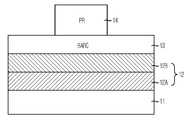
도 5a 내지 도 5c는 본 발명의 실시예에 따른 하드마스크를 이용한 패턴 형성 방법을 도시한 공정 단면도이다.5A to 5C are cross-sectional views illustrating a method of forming a pattern using a hard mask according to an exemplary embodiment of the present invention.
도 5a에 도시된 바와 같이, 다층의 하드마스크를 식각장벽으로 이용하여 패터닝될 피식각층(31)을 형성한다. 여기서, 피식각층(31)은 배리어메탈(B/M, 31A)과 텅스텐막(31B)의 적층이다. 배리어메탈(31A)은 티타늄(Ti)과 티타늄질화막(TiN)의 적층이 가능하다.As shown in FIG. 5A, an etched
이어서, 피식각층(31) 상에 다층의 하드마스크(32)를 형성한다. 이때, 다층의 하드마스크(32)의 제조 방법의 원리는 도 3a 내지 도 3c를 참조하기로 한다.Subsequently, a multi-layer
도 5a에서는 다층의 하드마스크(32)가 질화막(Nit, 32A), 텅스텐막(W H/M, 32B), 변형층(32C), 비정질카본(ACL, 32D) 및 SiON(32E)의 순서로 적층된 구조이며, 변형층(32C)은 텅스텐막(32B) 형성후에 표면처리를 통해 텅스텐막(32B)의 표면을 일정 두께 변형시킨 것이다. 표면처리는 비소(As), 인(Phosphorous, P) 또는 보론(Boron, B)과 같은 불순물을 함유한 가스를 이용한 이온주입법(Implant)을 이용하거나 또는 글로우방전(Glow discharge) 또는 플라즈마파워(Plasma power)를 이용하여 이온화시킨 입자를 표면에 입사시키는 플라즈마도핑법(Plasma Doping, PLAD)을 이용한다. 예를 들어, 표면처리를 위한 불순물 함유 가스는 PH3, AsH3, B2H6 또는 BF3 가스 중에서 선택된 어느 하나를 이용하며, 사용하는 에너지는 적어도 3KeV 이상이다. 한편, 플라즈마도핑법 사용시에는 아르곤(Ar) 가스를 첨가가스로 사용할 수 있다. 이와 같은 표면처리를 통해 텅스텐막(32B) 표면 내에 비소(As), 인(P) 또 는 보론(B)이 축적된 변형층(32C)을 형성하게 된다.In FIG. 5A, a multilayer
전술한 바와 같은 표면처리를 통해 형성되는 변형층(32C)에 의해 텅스텐막(32B)과 비정질카본(32D)간 직접적인 접촉을 방지하여 두 막간 비정상적인 결합에 의한 이물질의 생성을 억제한다. 아울러, 하드마스크(32)는 질화막(32A), 텅스텐막(32B), 변형층(32C), 비정질카본(32D) 및 SiON(32E)의 순서로 적층된 다층 구조이므로, 후속 자기정렬콘택식각 공정시 자기정렬콘택 마진을 충분히 확보할 수 있다.The
이어서, 다층의 하드마스크(32) 상에 노광공정시 난반사를 방지하기 위한 반사방지막인 BARC(33)를 형성한 후 감광막을 도포한다. 이후, 노광 및 현상으로 패터닝하여 감광막패턴(34)을 형성한다.Subsequently, after forming
도 5b에 도시된 바와 같이, 감광막패턴(34)을 식각장벽으로 하여 BARC(33)을 식각하고, 계속해서 SiON(32E) 및 비정질카본(32D)를 식각한다.As shown in FIG. 5B, the
이어서, 도 5c에 도시된 바와 같이, 남아있는 비정질카본(32D)를 식각장벽으로 배리어메탈(31A)까지 식각하여 패턴을 완성하는데, 일예로 형성되는 패턴은 비트라인 패턴이다. 여기서, 배리어메탈(31A)이 식각되는 시점에서 남아있는 하드마스크는 텅스텐막(32B)과 질화막(32A)이며, 텅스텐막(32B)은 후속 콘택홀 등의 자기정렬콘택식각공정에서 하드마스크로 사용된다.Subsequently, as shown in FIG. 5C, the remaining
상술한 실시예에 따르면, 다층의 하드마스크 적용시 다층의 하드마스크를 구성하고 있는 물질인 텅스텐막과 비정질카본 사이에 표면 처리를 통해 변형층을 형 성하므로써 텅스텐막을 하드마스크로 이용한 자기정렬콘택 식각 공정시의 자기정렬콘택마진 증가를 위한 역할은 유지하도록 하면서 비정질카본과의 비정상 결합에 의한 이물질이 발생할수 있는 원인을 제거할 수 있다.According to the above-described embodiments, self-aligned contact etching using a tungsten film as a hard mask by forming a strained layer through surface treatment between a tungsten film, which is a material constituting the multilayer hard mask, and an amorphous carbon, is applied when applying a multi-layer hard mask. While maintaining the role for increasing the self-aligned contact margin in the process, it is possible to eliminate the cause of foreign matters caused by abnormal bonding with amorphous carbon.
이상에서 설명한 본 발명은 전술한 실시예 및 첨부된 도면에 의해 한정되는 것이 아니고, 본 발명의 기술적 사상을 벗어나지 않는 범위 내에서 여러 가지 치환, 변형 및 변경이 가능하다는 것이 본 발명이 속하는 기술분야에서 통상의 지식을 가진 자에게 있어 명백할 것이다.The present invention described above is not limited to the above-described embodiments and the accompanying drawings, and various substitutions, modifications, and changes can be made in the art without departing from the technical spirit of the present invention. It will be clear to those of ordinary knowledge.
상술한 본 발명은 텅스텐막과 비정질카본을 포함하는 다층의 하드마스크 적용시 표면처리에 의한 변형층을 텅스텐막과 비정질카본 사이에 형성해주므로써 텅스텐막과 비정질카본간의 불균일을 제거하여 불필요한 이물질의 생성을 억제할 수 잇는 효과가 있다. 이로써, 다층의 하드마스크를 이용한 패턴 형성시에 안정적인 패턴을 형성할 수 있다.The present invention described above forms a deformed layer between the tungsten film and the amorphous carbon by surface treatment when applying a multi-layer hard mask including the tungsten film and the amorphous carbon to remove the unevenness between the tungsten film and the amorphous carbon to generate unnecessary foreign matter. There is an effect that can be suppressed. Thereby, a stable pattern can be formed at the time of pattern formation using a multilayer hard mask.
Claims (10)
Translated fromKoreanPriority Applications (2)
| Application Number | Priority Date | Filing Date | Title |
|---|---|---|---|
| KR1020060134340AKR100808056B1 (en) | 2006-12-27 | 2006-12-27 | Pattern formation method using hard mask |
| US11/823,770US7867911B2 (en) | 2006-12-27 | 2007-06-28 | Method for forming pattern using hard mask |
Applications Claiming Priority (1)
| Application Number | Priority Date | Filing Date | Title |
|---|---|---|---|
| KR1020060134340AKR100808056B1 (en) | 2006-12-27 | 2006-12-27 | Pattern formation method using hard mask |
Publications (1)
| Publication Number | Publication Date |
|---|---|
| KR100808056B1true KR100808056B1 (en) | 2008-02-28 |
Family
ID=39383538
Family Applications (1)
| Application Number | Title | Priority Date | Filing Date |
|---|---|---|---|
| KR1020060134340AExpired - Fee RelatedKR100808056B1 (en) | 2006-12-27 | 2006-12-27 | Pattern formation method using hard mask |
Country Status (2)
| Country | Link |
|---|---|
| US (1) | US7867911B2 (en) |
| KR (1) | KR100808056B1 (en) |
Families Citing this family (7)
| Publication number | Priority date | Publication date | Assignee | Title |
|---|---|---|---|---|
| KR101344019B1 (en)* | 2007-11-01 | 2013-12-24 | 삼성전자주식회사 | Method of implatating ions |
| US9034703B2 (en) | 2012-09-13 | 2015-05-19 | International Business Machines Corporation | Self aligned contact with improved robustness |
| US9431250B2 (en) | 2014-03-06 | 2016-08-30 | International Business Machines Corporation | Deep well implant using blocking mask |
| WO2018144198A1 (en)* | 2017-02-01 | 2018-08-09 | Applied Materials, Inc. | Boron doped tungsten carbide for hardmask applications |
| JP6883495B2 (en)* | 2017-09-04 | 2021-06-09 | 東京エレクトロン株式会社 | Etching method |
| CN114999912A (en)* | 2022-05-24 | 2022-09-02 | 长鑫存储技术有限公司 | Semiconductor structure and forming method thereof |
| KR20230165643A (en)* | 2022-05-27 | 2023-12-05 | 에스케이하이닉스 주식회사 | Methods of forming patterns by using hard mask |
Citations (5)
| Publication number | Priority date | Publication date | Assignee | Title |
|---|---|---|---|---|
| KR20030096765A (en)* | 2002-06-17 | 2003-12-31 | 동부전자 주식회사 | Method for forming diffused reflection film for the photo-resist pattern to be form precisely |
| KR20040057502A (en)* | 2002-12-26 | 2004-07-02 | 주식회사 하이닉스반도체 | A forming method of pattern of semiconductor device using ArF photolithography |
| KR20040057434A (en)* | 2002-12-26 | 2004-07-02 | 주식회사 하이닉스반도체 | Method for fabricating semiconductor device |
| KR20050019905A (en)* | 2002-07-31 | 2005-03-03 | 어드밴스드 마이크로 디바이시즈, 인코포레이티드 | Method for reducing pattern deformation and photoresist poisoning in semiconductor device fabrication |
| KR20060010932A (en)* | 2004-07-29 | 2006-02-03 | 주식회사 하이닉스반도체 | Method for manufacturing semiconductor device using amorphous carbon film as sacrificial hard mask |
Family Cites Families (4)
| Publication number | Priority date | Publication date | Assignee | Title |
|---|---|---|---|---|
| JP2737764B2 (en)* | 1995-03-03 | 1998-04-08 | 日本電気株式会社 | Semiconductor device and manufacturing method thereof |
| US7084071B1 (en)* | 2002-09-16 | 2006-08-01 | Advanced Micro Devices, Inc. | Use of multilayer amorphous carbon ARC stack to eliminate line warpage phenomenon |
| US7354631B2 (en)* | 2003-11-06 | 2008-04-08 | Micron Technology, Inc. | Chemical vapor deposition apparatus and methods |
| US7064078B2 (en)* | 2004-01-30 | 2006-06-20 | Applied Materials | Techniques for the use of amorphous carbon (APF) for various etch and litho integration scheme |
- 2006
- 2006-12-27KRKR1020060134340Apatent/KR100808056B1/ennot_activeExpired - Fee Related
- 2007
- 2007-06-28USUS11/823,770patent/US7867911B2/ennot_activeExpired - Fee Related
Patent Citations (5)
| Publication number | Priority date | Publication date | Assignee | Title |
|---|---|---|---|---|
| KR20030096765A (en)* | 2002-06-17 | 2003-12-31 | 동부전자 주식회사 | Method for forming diffused reflection film for the photo-resist pattern to be form precisely |
| KR20050019905A (en)* | 2002-07-31 | 2005-03-03 | 어드밴스드 마이크로 디바이시즈, 인코포레이티드 | Method for reducing pattern deformation and photoresist poisoning in semiconductor device fabrication |
| KR20040057502A (en)* | 2002-12-26 | 2004-07-02 | 주식회사 하이닉스반도체 | A forming method of pattern of semiconductor device using ArF photolithography |
| KR20040057434A (en)* | 2002-12-26 | 2004-07-02 | 주식회사 하이닉스반도체 | Method for fabricating semiconductor device |
| KR20060010932A (en)* | 2004-07-29 | 2006-02-03 | 주식회사 하이닉스반도체 | Method for manufacturing semiconductor device using amorphous carbon film as sacrificial hard mask |
Also Published As
| Publication number | Publication date |
|---|---|
| US20080160778A1 (en) | 2008-07-03 |
| US7867911B2 (en) | 2011-01-11 |
Similar Documents
| Publication | Publication Date | Title |
|---|---|---|
| KR100808056B1 (en) | Pattern formation method using hard mask | |
| TWI636485B (en) | Development of high etch selective hardmask material by ion implantation into amorphous carbon films | |
| US7553771B2 (en) | Method of forming pattern of semiconductor device | |
| KR100268923B1 (en) | method for forming dual gate of semiconductor device | |
| KR101708206B1 (en) | Semiconductor device manufacturing method | |
| KR100306990B1 (en) | Method for fabricating semiconductor device | |
| KR20090009388A (en) | Manufacturing method of semiconductor device | |
| US6664602B2 (en) | Semiconductor device and method of manufacturing the same | |
| CN115020335B (en) | Method of forming a semiconductor structure | |
| US20070054444A1 (en) | Manufacturing method of a semiconductor device | |
| KR100712978B1 (en) | Semiconductor device manufacturing method | |
| US7144820B2 (en) | Method of manufacturing a layer sequence and a method of manufacturing an integrated circuit | |
| US7329618B2 (en) | Ion implanting methods | |
| US7563708B2 (en) | Method for manufacturing semiconductor device | |
| KR20050067451A (en) | Semiconductor device and fabricating method thereof | |
| US20080012143A1 (en) | Semiconductor Device and Method of Fabricating the Same | |
| KR20010008442A (en) | Transistor Formation Method of Semiconductor Device | |
| KR100390901B1 (en) | Method for manufactruing transistor in sram device | |
| KR20020058359A (en) | Method For Treatment The Temperature Of Source/Drain Region | |
| KR100721621B1 (en) | Method of forming buried contacts in semiconductor devices | |
| KR20020002065A (en) | Method for manufacturing a pmos transistor | |
| KR20010063501A (en) | self-aligned contact of bit line in memory device | |
| KR20090000427A (en) | PMOS transistor manufacturing method | |
| KR20010008561A (en) | Method For Forming The Contact Hole Of Semiconductor Device | |
| KR20030092530A (en) | Method for forming poly pattern of semiconductor device |
Legal Events
| Date | Code | Title | Description |
|---|---|---|---|
| A201 | Request for examination | ||
| PA0109 | Patent application | St.27 status event code:A-0-1-A10-A12-nap-PA0109 | |
| PA0201 | Request for examination | St.27 status event code:A-1-2-D10-D11-exm-PA0201 | |
| E902 | Notification of reason for refusal | ||
| PE0902 | Notice of grounds for rejection | St.27 status event code:A-1-2-D10-D21-exm-PE0902 | |
| E13-X000 | Pre-grant limitation requested | St.27 status event code:A-2-3-E10-E13-lim-X000 | |
| P11-X000 | Amendment of application requested | St.27 status event code:A-2-2-P10-P11-nap-X000 | |
| P13-X000 | Application amended | St.27 status event code:A-2-2-P10-P13-nap-X000 | |
| E701 | Decision to grant or registration of patent right | ||
| PE0701 | Decision of registration | St.27 status event code:A-1-2-D10-D22-exm-PE0701 | |
| GRNT | Written decision to grant | ||
| PR0701 | Registration of establishment | St.27 status event code:A-2-4-F10-F11-exm-PR0701 | |
| PR1002 | Payment of registration fee | St.27 status event code:A-2-2-U10-U11-oth-PR1002 Fee payment year number:1 | |
| PG1601 | Publication of registration | St.27 status event code:A-4-4-Q10-Q13-nap-PG1601 | |
| PR1001 | Payment of annual fee | St.27 status event code:A-4-4-U10-U11-oth-PR1001 Fee payment year number:4 | |
| FPAY | Annual fee payment | Payment date:20120127 Year of fee payment:5 | |
| PR1001 | Payment of annual fee | St.27 status event code:A-4-4-U10-U11-oth-PR1001 Fee payment year number:5 | |
| PN2301 | Change of applicant | St.27 status event code:A-5-5-R10-R13-asn-PN2301 St.27 status event code:A-5-5-R10-R11-asn-PN2301 | |
| PN2301 | Change of applicant | St.27 status event code:A-5-5-R10-R13-asn-PN2301 St.27 status event code:A-5-5-R10-R11-asn-PN2301 | |
| LAPS | Lapse due to unpaid annual fee | ||
| PC1903 | Unpaid annual fee | St.27 status event code:A-4-4-U10-U13-oth-PC1903 Not in force date:20130222 Payment event data comment text:Termination Category : DEFAULT_OF_REGISTRATION_FEE | |
| PC1903 | Unpaid annual fee | St.27 status event code:N-4-6-H10-H13-oth-PC1903 Ip right cessation event data comment text:Termination Category : DEFAULT_OF_REGISTRATION_FEE Not in force date:20130222 | |
| PN2301 | Change of applicant | St.27 status event code:A-5-5-R10-R13-asn-PN2301 St.27 status event code:A-5-5-R10-R11-asn-PN2301 |