KR100806343B1 - Memory system including flash memory and its mapping table management method - Google Patents
Memory system including flash memory and its mapping table management methodDownload PDFInfo
- Publication number
- KR100806343B1 KR100806343B1KR1020060101961AKR20060101961AKR100806343B1KR 100806343 B1KR100806343 B1KR 100806343B1KR 1020060101961 AKR1020060101961 AKR 1020060101961AKR 20060101961 AKR20060101961 AKR 20060101961AKR 100806343 B1KR100806343 B1KR 100806343B1
- Authority
- KR
- South Korea
- Prior art keywords
- block
- page
- mapping table
- memory
- order
- Prior art date
- Legal status (The legal status is an assumption and is not a legal conclusion. Google has not performed a legal analysis and makes no representation as to the accuracy of the status listed.)
- Expired - Fee Related
Links
Images


Classifications
- G—PHYSICS
- G06—COMPUTING OR CALCULATING; COUNTING
- G06F—ELECTRIC DIGITAL DATA PROCESSING
- G06F12/00—Accessing, addressing or allocating within memory systems or architectures
- G06F12/02—Addressing or allocation; Relocation
- G06F12/0223—User address space allocation, e.g. contiguous or non contiguous base addressing
- G06F12/023—Free address space management
- G06F12/0238—Memory management in non-volatile memory, e.g. resistive RAM or ferroelectric memory
- G06F12/0246—Memory management in non-volatile memory, e.g. resistive RAM or ferroelectric memory in block erasable memory, e.g. flash memory
- G—PHYSICS
- G06—COMPUTING OR CALCULATING; COUNTING
- G06F—ELECTRIC DIGITAL DATA PROCESSING
- G06F12/00—Accessing, addressing or allocating within memory systems or architectures
- G—PHYSICS
- G06—COMPUTING OR CALCULATING; COUNTING
- G06F—ELECTRIC DIGITAL DATA PROCESSING
- G06F12/00—Accessing, addressing or allocating within memory systems or architectures
- G06F12/02—Addressing or allocation; Relocation
- G06F12/0223—User address space allocation, e.g. contiguous or non contiguous base addressing
- G06F12/0292—User address space allocation, e.g. contiguous or non contiguous base addressing using tables or multilevel address translation means
- G—PHYSICS
- G06—COMPUTING OR CALCULATING; COUNTING
- G06F—ELECTRIC DIGITAL DATA PROCESSING
- G06F2212/00—Indexing scheme relating to accessing, addressing or allocation within memory systems or architectures
- G06F2212/72—Details relating to flash memory management
- G06F2212/7201—Logical to physical mapping or translation of blocks or pages
Landscapes
- Engineering & Computer Science (AREA)
- Theoretical Computer Science (AREA)
- Physics & Mathematics (AREA)
- General Engineering & Computer Science (AREA)
- General Physics & Mathematics (AREA)
- Memory System (AREA)
Abstract
Translated fromKoreanDescription
Translated fromKorean도 1은 일반적인 플래시 메모리를 사용하는 메모리 시스템의 하드웨어 구조를 보여주는 블록도이다.1 is a block diagram illustrating a hardware structure of a memory system using a general flash memory.
도 2는 일반적인 플래시 메모리를 사용하는 메모리 시스템의 소프트웨어 구조를 보여주는 블록도이다.2 is a block diagram showing a software structure of a memory system using a general flash memory.
도 3은 일반적인 혼합 맵핑 방법을 수행하는 메모리 시스템을 보여주는 블록도이다.3 is a block diagram illustrating a memory system that performs a general mixed mapping method.
도 4는 도 3에 도시된 메모리 시스템의 혼합 맵핑 방법을 예시적으로 설명하기 위한 다이어그램이다.FIG. 4 is a diagram for exemplarily describing a mixed mapping method of the memory system illustrated in FIG. 3.
도 5는 본 발명에 따른 혼합 맵핑 동작을 사용하는 메모리 시스템을 보여주는 블록도이다.5 is a block diagram illustrating a memory system using a mixed mapping operation according to the present invention.
도 6은 도 5에 도시된 메모리 시스템의 맵핑 테이블 관리 방법을 예시적으로 보여주는 도표이다.FIG. 6 is a diagram exemplarily illustrating a method of managing a mapping table of the memory system illustrated in FIG. 5.
도 7은 도 5에 도시된 메모리 시스템의 혼합 맵핑 동작을 예시적으로 설명하기 위한 다이어그램이다.FIG. 7 is a diagram for exemplarily describing a mixed mapping operation of the memory system illustrated in FIG. 5.
* 도면의 주요 부분에 대한 부호 설명 *Explanation of symbols on the main parts of the drawings
300, 400; 메모리 시스템 310, 410; 파일 시스템300, 400;
320, 420; 플래시 변환 레이어 330, 430; 플래시 메모리320, 420; Flash
321, 421; 블록 맵핑 테이블 322; 페이지 맵핑 테이블321, 421; Block mapping table 322; Page mapping table
422; 랩-어라운드 페이지 맵핑 테이블 423; 랜덤 페이지 맵핑 테이블422; Wrap-around page mapping table 423; Random page mapping table
본 발명은 플래시 메모리를 사용한 메모리 시스템에 관한 것으로, 더욱 상세하게는 메모리 시스템 및 그것의 맵핑 테이블 관리 방법에 관한 것이다.The present invention relates to a memory system using a flash memory, and more particularly to a memory system and a mapping table management method thereof.
최근 디지털 카메라, MP3 플레이어, 핸드폰, PDA 등과 같은 휴대 장치가 많이 사용되고 있다. 플래시 메모리는 저전력, 비휘발성, 고집적 등의 특성으로 인해 이러한 휴대 장치에 많이 사용되고 있다. 특히, 플래시 메모리의 용량이 크게 늘어나면서 디스크를 플래시 메모리로 대체하는 경향이 많아지고 있다.Recently, portable devices such as digital cameras, MP3 players, mobile phones, PDAs, and the like have been widely used. Flash memory is widely used in such portable devices because of its low power, nonvolatile and high integration characteristics. In particular, as the capacity of a flash memory increases significantly, there is a tendency to replace a disk with a flash memory.
플래시 메모리는 물리적 특성으로 인하여 쓰기 전 소거(erase-before-write) 연산을 수행한다. 즉, 플래시 메모리는 섹터(sector, 보통 512 바이트)에 쓰기 동작을 수행할 경우, 그 섹터가 속한 블록(block)을 소거한 다음에, 쓰기 동작을 수행한다. 따라서 플래시 메모리는, 섹터에 덮어 쓰기(over write)를 수행할 수 있는 하드 디스크에 비하여, 동일한 I/O에 대해 더 많은 시간을 필요로 한다. 또한, 플래시 메모리는 동일한 블록에 대해 10만 번 정도의 소거 동작을 수행하면, 더 이상 사용할 수 없다. 따라서 플래시 메모리는 특정 블록에 대해 소거 동작이 반복되는 것을 피해야 한다.Flash memory performs erase-before-write operations due to physical characteristics. That is, when performing a write operation on a sector (typically 512 bytes), the flash memory erases a block to which the sector belongs, and then performs a write operation. Thus, flash memory requires more time for the same I / O than hard disks capable of overwriting sectors. In addition, the flash memory may not be used any more when 100,000 erase operations are performed on the same block. Therefore, the flash memory should avoid repeating the erase operation for a specific block.
플래시 변환 레이어(Flash Translation Layer; FTL)는 플래시 메모리의 이러한 단점을 극복하고, 플래시 메모리를 효율적으로 관리하기 위한 소프트웨어이다. 플래시 변환 레이어(FTL)는 파일 시스템(File System)으로부터 논리적 섹터 번호(Logical Sector Number; LSN)를 입력받고, 이를 물리적 섹터 번호(Physical Sector Number; PSN)로 변환한다. 물리적 섹터 번호(PSN)는 실제 플래시 메모리에서 사용할 어드레스이다.Flash Translation Layer (FTL) is software for overcoming these shortcomings of flash memory and for efficient management of flash memory. The flash translation layer FTL receives a logical sector number (LSN) from a file system and converts the logical sector number (PSN) into a physical sector number (PSN). The physical sector number (PSN) is an address to use in the actual flash memory.
플래시 변환 레이어(FTL)는 위와 같은 어드레스 변환을 위해 어드레스 맵핑 테이블(Address Mapping Table)을 갖는다. 어드레스 맵핑 테이블은 랜덤 액세스 메모리(RAM)에 저장된다. 어드레스 맵핑 테이블에는 논리적 어드레스(Logical Address) 및 이에 대응하는 물리적 어드레스(Physical Address)가 표시되어 있다. 어드레스 맵핑 테이블은 맵핑 단위에 따라 그 크기가 달라질 수 있으며, 맵핑 단위에 따라 다양한 맵핑 방법을 갖는다.The flash translation layer FTL has an address mapping table for address conversion as described above. The address mapping table is stored in random access memory (RAM). In the address mapping table, a logical address and a corresponding physical address are displayed. The size of the address mapping table may vary depending on the mapping unit, and has various mapping methods according to the mapping unit.
대표적인 맵핑 방법으로, 페이지 맵핑 방법(page mapping method), 블록 맵핑 방법(block mapping method), 그리고 혼합 맵핑 방법(hybrid mapping method)이 있다. 페이지 맵핑 방법은 페이지 단위로 맵핑 테이블을 만들고, 논리적 페이지를 물리적 페이지로 변환하는 방법이다. 블록 맵핑 방법은 블록 단위로 맵핑 동작을 수행하는 방법이다. 혼합 맵핑 방법은 페이지 맵핑 방법과 블록 맵핑 방법을 동시에 사용하는 방법이다.Typical mapping methods include a page mapping method, a block mapping method, and a hybrid mapping method. Page mapping method creates mapping table by page and converts logical page into physical page. The block mapping method is a method of performing a mapping operation in units of blocks. The mixed mapping method uses a page mapping method and a block mapping method at the same time.
일반적으로 하나의 메모리 블록은 수십 또는 수백 개의 페이지로 구성된다. 따라서 페이지 맵핑 방법을 사용할 경우에, 맵핑 테이블의 크기는 블록 맵핑 방법을 사용할 때보다 수십 또는 수백 배 증가하게 된다. 즉, 페이지 맵핑 방법은 맵핑 테이블을 사용하는 데 너무 많은 메모리 공간을 필요로 한다는 단점을 갖는다.Typically, one memory block consists of tens or hundreds of pages. Therefore, when using the page mapping method, the size of the mapping table is increased by tens or hundreds of times than when using the block mapping method. That is, the page mapping method has a disadvantage in that it requires too much memory space to use the mapping table.
반면, 블록 맵핑 방법은 블록 단위로 맵핑 동작을 수행하기 때문에, 페이지 맵핑 방법에 비해 맵핑 테이블의 크기를 줄일 수 있는 장점을 갖는다. 그러나 블록 맵핑 방법에 의하면, 블록 내에 쓰여질 페이지의 위치가 고정되기 때문에, 많은 머지(merge) 연산을 수행해야 한다는 단점을 갖는다.On the other hand, since the block mapping method performs the mapping operation in units of blocks, the size of the mapping table can be reduced compared to the page mapping method. However, the block mapping method has a disadvantage in that a large number of merge operations must be performed because the position of the page to be written in the block is fixed.
혼합 맵핑 방법은 로그 블록(log block)에 대해서는 페이지 맵핑 방법을 사용하고, 데이터 블록(data block)에 대해서는 블록 맵핑 방법을 사용한다. 혼합 맵핑 방법은 두 가지 맵핑 방법을 모두 사용함으로, 맵핑 테이블의 크기를 줄임과 동시에, 머지 연산의 횟수를 줄일 수 있다.The mixed mapping method uses a page mapping method for log blocks and a block mapping method for data blocks. The hybrid mapping method uses both mapping methods, thereby reducing the size of the mapping table and reducing the number of merge operations.
여기에서, 로그 블록은 일종의 쓰기 버퍼와 같은 기능을 한다. 즉 쓰기 동작 시에, 데이터 블록에 저장될 페이지 데이터는 먼저 로그 블록에 저장된다. 로그 블록 및 이에 대응하는 데이터 블록(이하, 구 데이터 블록, old data block)에 저장된 페이지 데이터는 머지 연산을 통해 새 데이터 블록(new data block)에 저장된다. 머지 연산 후에, 로그 블록 및 데이터 블록은 소거된다.Here, the log block acts as a kind of write buffer. That is, in the write operation, the page data to be stored in the data block is first stored in the log block. Page data stored in a log block and a corresponding data block (hereinafter, old data block) are stored in a new data block through a merge operation. After the merge operation, log blocks and data blocks are erased.
이와 같이 혼합 맵핑 방법을 사용하면, 복수의 페이지 복사 및 복수의 블록 소거 동작이 수행된다. 예를 들어, 하나의 블록이 4개의 페이지로 구성되어 있다고 가정하면, 위의 예에서 4번의 페이지 복사 및 2번의 블록 소거 동작이 수행된다. 혼합 맵핑 방법을 사용함에 있어서, 많은 수의 페이지 복사 및 블록 소거 동작은 전체 메모리 시스템의 성능을 저하하는 요인이 되고 있다.Using the mixed mapping method as described above, a plurality of page copies and a plurality of block erase operations are performed. For example, assuming that one block is composed of four pages, four page copies and two block erase operations are performed in the above example. In using the mixed mapping method, a large number of page copy and block erase operations are degrading the performance of the entire memory system.
본 발명의 목적은 혼합 맵핑 방법을 사용함에 있어서, 불필요한 페이지 복사 및 블록 소거 동작을 줄일 수 있는 메모리 시스템 및 그것의 맵핑 테이블 관리 방법을 제공하는 데 있다.An object of the present invention is to provide a memory system and a mapping table management method thereof that can reduce unnecessary page copy and block erase operations in using a mixed mapping method.
본 발명에 따른 메모리 시스템은 파일 시스템; 상기 파일 시스템으로부터 논리적 어드레스를 입력받고, 상기 논리적 어드레스를 물리적 어드레스로 변환하는 플래시 변환 레이어; 및 상기 변환된 물리적 어드레스를 입력받는 플래시 메모리를 포함한다. 여기에서, 상기 플래시 변환 레이어는 상기 플래시 메모리의 메모리 블록 내의 페이지 순서가 랩-어라운드 방식(wrap-around order)임을 표시한 플래그 정보와, 상기 메모리 블록의 시작 페이지를 지정한 오프셋 정보를 갖는다.A memory system according to the present invention includes a file system; A flash translation layer that receives a logical address from the file system and converts the logical address into a physical address; And a flash memory receiving the converted physical address. Here, the flash conversion layer has flag information indicating that a page order in a memory block of the flash memory is a wrap-around order, and offset information designating a start page of the memory block.
실시예로서, 상기 플래시 변환 레이어는 논리적 블록 어드레스를 물리적 블록 어드레스로 변환하기 위한 블록 맵핑 테이블; 및 상기 메모리 블록의 시작 페이지를 지정하기 위한 오프셋 정보를 저장하는 랩-어라운드 페이지 맵핑 테이블을 포함한다. 상기 블록 맵핑 테이블은 순차 위치 방식(in-place order)임을 표시하는 제 1 플래그 정보; 및 상기 랩-어라운드 방식임을 표시하는 제 2 플래그 정보를 갖는다. 상기 블록 맵핑 테이블은 임의 위치 방식(out-of-place order)임을 표시하는 제 3 플래그 정보를 더 갖는다. 상기 플래시 변환 레이어는 상기 임의 위치 방식에 사용될 오프셋 정보를 저장하기 위한 랜덤 페이지 맵핑 테이블을 더 포함한다.In an embodiment, the flash translation layer includes a block mapping table for converting a logical block address into a physical block address; And a wrap-around page mapping table that stores offset information for designating a start page of the memory block. The block mapping table includes first flag information indicating an in-place order; And second flag information indicating the wrap-around scheme. The block mapping table further has third flag information indicating an out-of-place order. The flash translation layer further includes a random page mapping table for storing offset information to be used in the random position scheme.
본 발명은 메모리 시스템의 맵핑 테이블 관리 방법에 관한 것이다. 상기 메모리 시스템은 파일 시스템; 상기 파일 시스템으로부터 논리적 어드레스를 입력받고, 상기 논리적 어드레스를 물리적 어드레스로 변환하는 플래시 변환 레이어; 및 상기 변환된 물리적 어드레스를 입력받는 플래시 메모리를 포함한다.The present invention relates to a mapping table management method of a memory system. The memory system comprises a file system; A flash translation layer that receives a logical address from the file system and converts the logical address into a physical address; And a flash memory receiving the converted physical address.
상기 메모리 시스템의 맵핑 테이블 관리 방법은 상기 논리적 어드레스를 입력받고, 상기 물리적 어드레스를 찾는 단계; 상기 물리적 어드레스에 해당하는 메모리 블록 내의 페이지 순서가 랩-어라운드 방식임을 표시하는지를 확인하는 단계; 상기 메모리 블록 내의 페이지 순서가 랩-어라운드 방식(wrap-around order)인 경우에, 상기 메모리 블록의 시작 페이지를 찾는 단계; 및 상기 메모리 블록 내의 페이지 순서를 알고, 원하는 페이지를 읽는 단계를 포함한다.The method of managing a mapping table of the memory system may include receiving the logical address and finding the physical address; Checking whether a page order in a memory block corresponding to the physical address indicates a wrap-around scheme; Finding a start page of the memory block if the page order in the memory block is a wrap-around order; And knowing a page order in the memory block and reading a desired page.
실시예로서, 상기 플래시 변환 레이어는 상기 플래시 메모리의 메모리 블록 내의 페이지 순서가 랩-어라운드 방식(wrap-around order)임을 표시한 플래그 정보와, 상기 메모리 블록의 시작 페이지를 지정한 오프셋 정보를 갖는다. 상기 플래시 변환 레이어는 논리적 블록 어드레스를 물리적 블록 어드레스로 변환하기 위한 블록 맵핑 테이블; 및 상기 메모리 블록의 시작 페이지를 지정하기 위한 오프셋 정보를 저장하는 랩-어라운드 페이지 맵핑 테이블을 포함한다. 상기 블록 맵핑 테이블은 순차 위치 방식(in-place order)임을 표시하는 제 1 플래그 정보; 및 상기 랩-어라운드 방식임을 표시하는 제 2 플래그 정보를 저장한다.In example embodiments, the flash translation layer may include flag information indicating that a page order in a memory block of the flash memory is a wrap-around order, and offset information designating a start page of the memory block. The flash translation layer includes a block mapping table for converting a logical block address into a physical block address; And a wrap-around page mapping table that stores offset information for designating a start page of the memory block. The block mapping table includes first flag information indicating an in-place order; And second flag information indicating that the wrap-around method is used.
다른 실시예로서, 상기 메모리 블록 내의 페이지 순서가 순차 위치 방식(in- place order)인 경우에, 원하는 페이지를 읽는 단계를 더 포함한다. 상기 플래시 변환 레이어는 상기 순차 위치 방식(in-place order)임을 표시한 플래그 정보를 갖는다. 상기 플래시 변환 레이어는 상기 플래그 정보를 블록 맵핑 테이블에 기록한다.In another embodiment, the method may further include reading a desired page when the page order in the memory block is an in-place order. The flash conversion layer has flag information indicating that the in-place order. The flash translation layer writes the flag information in a block mapping table.
또 다른 실시예로서, 상기 플래시 변환 레이어는 논리적 블록 어드레스를 물리적 블록 어드레스로 변환하기 위한 블록 맵핑 테이블; 상기 메모리 블록의 시작 페이지를 지정하기 위한 오프셋 정보를 저장하는 랩-어라운드 페이지 맵핑 테이블; 및 임의 위치 방식에 따른 오프셋 정보를 저장하기 위한 랜덤 페이지 맵핑 테이블을 포함한다. 상기 블록 맵핑 테이블은 상기 순차 위치 방식(in-place order)임을 표시하는 제 1 플래그 정보; 상기 랩-어라운드 방식임을 표시하는 제 2 플래그 정보; 및 상기 임의 위치 방식(out-of-place order)임을 표시하는 제 3 플래그 정보를 갖는다.In another embodiment, the flash translation layer includes a block mapping table for translating a logical block address into a physical block address; A wrap-around page mapping table that stores offset information for designating a start page of the memory block; And a random page mapping table for storing offset information according to an arbitrary position method. The block mapping table includes first flag information indicating that the block mapping table is in an in-place order; Second flag information indicating the wrap-around scheme; And third flag information indicating the out-of-place order.
이하, 본 발명이 속하는 기술분야에서 통상의 지식을 가진 자가 본 발명의 기술적 사상을 용이하게 실시할 수 있을 정도로 상세히 설명하기 위하여, 본 발명의 바람직한 실시예를 첨부된 도면을 참조하여 설명하기로 한다.DETAILED DESCRIPTION Hereinafter, exemplary embodiments of the present invention will be described with reference to the accompanying drawings so that those skilled in the art can easily implement the technical idea of the present invention. .
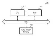
도 1은 일반적인 플래시 메모리를 사용하는 메모리 시스템의 하드웨어 구조를 보여주는 블록도이다. 도 1을 참조하면, 메모리 시스템(100)은 중앙처리장치(110), 랜덤 액세스 메모리(120), 그리고 낸드 플래시 메모리(130)를 포함한다. 어드레스 맵핑 동작을 위한 플래시 변환 레이어(FTL)는 랜덤 액세스 메모리(120)에 저장된다.1 is a block diagram illustrating a hardware structure of a memory system using a general flash memory. Referring to FIG. 1, the
낸드 플래시 메모리(130)는 당업자에게 잘 알려진 바와 같이, 스트링 구조(string structure)를 갖는 복수의 메모리 셀로 구성된다. 이러한 메모리 셀들의 집합을 셀 어레이(cell array)라고 부른다. 낸드 플래시 메모리(130)의 메모리 셀 어레이는 복수의 메모리 블록(memory block)으로 구성된다. 각각의 메모리 블록은 복수의 페이지(page)로 구성된다. 각각의 페이지는 하나의 워드 라인을 공유하는 복수의 메모리 셀로 구성된다.
낸드 플래시 메모리(130)는 읽기 및 쓰기 동작의 단위와 소거 동작의 단위가 다르다. 즉, 낸드 플래시 메모리(130)는 메모리 블록 단위로 소거 동작을 수행하고, 페이지 단위로 읽기 및 쓰기 동작을 수행한다. 또한, 낸드 플래시 메모리(130)는 다른 반도체 메모리 장치와 달리 겹쳐 쓰기(over write)를 지원하지 않는다. 따라서 낸드 플래시 메모리(130)는 쓰기 동작 전에 소거 동작을 수행한다.The
낸드 플래시 메모리(130)의 이와 같은 특성으로 인해, 낸드 플래시 메모리(130)를 하드 디스크처럼 사용하기 위해서는, 읽기/쓰기/소거 동작에 대한 별도의 관리가 필요하다. 플래시 변환 레이어(Flash Translation Layer; 이하 FTL이라 함)는 이러한 목적으로 개발된 시스템 소프트웨어이다.Due to such characteristics of the
낸드 플래시 메모리(130)는 데이터 영역, 로그 영역, 그리고 메타 영역을 포함한다. 데이터 영역은 복수의 데이터 블록으로 구성되며, 사용자 데이터를 저장한다. 로그 영역은 하나 또는 그 이상의 로그 블록으로 구성된다. 로그 블록은 특정 데이터 블록에 할당되어 진다.The
특정 데이터 블록에 데이터를 쓰고자 하는 경우, 데이터는 특정 데이터 블록 에 직접 쓰여 지는 것이 아니라, 할당되어 있는 로그 블록에 먼저 저장된다. 그 다음에, 머지(merge) 동작을 통해, 로그 블록의 유효한 페이지와 데이터 블록의 유효한 페이지가 새로운 데이터 블록으로 복사된다. 머지 동작이 수행되면, 맵핑 정보가 변경되는데, 변경된 맵핑 정보는 메타 영역에 저장된다.If you want to write data to a specific data block, the data is not written directly to the specific data block, but rather stored first in the assigned log block. Then, through a merge operation, valid pages of the log block and valid pages of the data block are copied into the new data block. When the merge operation is performed, the mapping information is changed, and the changed mapping information is stored in the meta area.
도 2는 일반적인 플래시 메모리를 사용하는 메모리 시스템의 소프트웨어 구조를 보여주는 블록도이다. 도 2를 참조하면, 플래시 변환 레이어(FTL, 220)는 애플리케이션(205) 또는 파일 시스템(210)으로부터 논리적 어드레스를 입력받고, 이를 물리적 어드레스로 변환한 다음에, 변환한 물리적 어드레스를 낸드 플래시 메모리(230)로 제공한다.2 is a block diagram showing a software structure of a memory system using a general flash memory. Referring to FIG. 2, the flash
어드레스 변환을 위한 맵핑 테이블은 도 1에 도시된 랜덤 액세스 메모리(120)에 저장된다. 맵핑 방법에는 맵핑 단위에 따라 여러 가지 방식이 있다. 예를 들면, 페이지 단위로 맵핑 동작을 수행하는 페이지 맵핑 방법(page mapping method), 블록 단위로 맵핑 동작을 수행하는 블록 맵핑 방법(block mapping method), 그리고 두 가지를 모두 사용하는 혼합 맵핑 방법(hybrid mapping method)이 있다.The mapping table for address translation is stored in the
페이지 맵핑 방법은 페이지 맵핑 테이블을 위해 많은 메모리 공간을 필요로 한다는 단점을 갖는다. 블록 맵핑 방법은 메모리 공간을 줄일 수 있지만, 많은 머지(merge) 동작을 수행한다는 단점을 갖는다. 혼합 맵핑 방법은 로그 블록(log block)에 대해서는 페이지 맵핑 방법을 사용한다. 혼합 맵핑 방법은 두 가지 맵핑 방법을 사용함으로, 맵핑 테이블의 크기를 줄임과 동시에, 머지 연산의 횟수를 줄 일 수 있다.The page mapping method has a disadvantage of requiring a lot of memory space for the page mapping table. The block mapping method can reduce memory space, but has a disadvantage of performing a lot of merge operations. The mixed mapping method uses a page mapping method for log blocks. The hybrid mapping method uses two mapping methods, thereby reducing the size of the mapping table and reducing the number of merge operations.
도 3은 일반적인 혼합 맵핑 방법을 수행하는 메모리 시스템을 보여주는 블록도이다. 도 3을 참조하면, 메모리 시스템(300)은 파일 시스템(310), 플래시 변환 레이어(320), 그리고 플래시 메모리(330)를 포함한다.3 is a block diagram illustrating a memory system that performs a general mixed mapping method. Referring to FIG. 3, the
플래시 변환 레이어(320)는 파일 시스템(310)으로부터 논리적 섹터 번호(Logical Sector Number; LSN)를 입력받는다. 플래시 변환 레이어(320)는 맵핑 테이블을 사용하여 논리적 섹터 번호(LSN)를 물리적 섹터 번호(Physical Sector Number; PSN)로 변환한다. 플래시 변환 레이어(320)는 물리적 섹터 번호(PSN)를 플래시 메모리(330)로 제공한다.The
도 3을 참조하면, 플래시 변환 레이어(320)는 블록 맵핑 테이블(321) 및 페이지 맵핑 테이블(322)을 포함한다. 여기에서, 페이지 맵핑 테이블(322)은 로그 블록의 페이지 맵핑을 위한 것이다. 로그 블록의 페이지 쓰기 동작 및 혼합 맵핑 동작은 도 4를 참조하여, 상세히 설명된다.Referring to FIG. 3, the
도 4는 도 3에 도시된 메모리 시스템의 혼합 맵핑 방법을 예시적으로 설명하기 위한 다이어그램이다. 도 4에서, 로그 블록(410) 및 데이터 블록(420)은 각각 4개의 페이지로 구성된다고 가정한다. 그리고 로그 블록(410)은 데이터 블록(420)에 할당되어 있다고 가정한다.FIG. 4 is a diagram for exemplarily describing a mixed mapping method of the memory system illustrated in FIG. 3. In FIG. 4, it is assumed that the
먼저, 쓰기 요청(write request)이 들어오면, 플래시 변환 레이어(도 3 참조, 320)는 데이터 블록(420)에 할당되어 있는 로그 블록(410)이 존재하는지를 검사한다. 검사 결과, 할당된 로그 블록(410)이 존재하면, 할당된 로그 블록(410)에 페이지 쓰기 동작을 수행한다. 만약, 할당된 로그 블록이 존재하지 않으면, 새로운 로그 블록을 할당받아 소거 동작을 수행한 다음에, 페이지 쓰기 동작을 수행한다.First, when a write request comes in, the flash translation layer 320 (see FIG. 3) checks whether a
도 4를 참조하면, 파일 시스템(도 3 참조, 310)은 2번, 3번, 0번, 1번 논리적 페이지 순서로 쓰기 요청을 하고 있다. 여기에서, 1번 논리적 페이지는 데이터는 데이터 블록(420)의 두 번째 물리적 페이지(이하, 제 2 물리적 페이지라 함)에 저장되어 있다.Referring to FIG. 4, the file system 310 (see FIG. 3) makes a write request in the order of
2번 논리적 페이지에 대한 쓰기 요청이 들어오면, 로그 블록(410)의 첫 번째 물리적 페이지(이하, 제 1 물리적 페이지라 함)에 대한 쓰기 동작이 수행된다. 다음으로, 3번 논리적 페이지에 대한 쓰기 요청이 들어오면, 로그 블록(410)의 제 2 물리적 페이지에 대한 쓰기 동작이 수행된다. 그리고 0번 논리적 페이지에 대한 쓰기 요청이 들어오면, 로그 블록(410)의 세 번째 물리적 페이지(이하 제 3 물리적 페이지라 함)에 대한 쓰기 동작이 수행된다.When a write request for
이때, 전체 로그 블록이 부족하여, 로그 블록(410)을 자유 블록(free block)으로 만들어야 하는 상황이 발생한다면, 플래시 변환 레이어(320)는 머지 동작을 수행한다. 즉, 로그 블록(410)의 제 1 내지 제 3 물리적 페이지에 저장된 2번, 3번, 0번 논리적 페이지와 데이터 블록(420)의 제 2 물리적 페이지에 저장된 1번 논리적 페이지는 새로운 데이터 블록(430)으로 복사된다.At this time, if there is a shortage of the entire log block and a situation in which the
먼저, 논리 블록(410)의 0번 페이지가 새로운 데이터 블록(430)의 제 1 물리적 페이지에 복사된다. 다음에, 데이터 블록(420)의 1번 페이지가 새로운 데이터 블록(430)의 제 2 물리적 페이지에 복사된다. 다음에, 논리 블록(410)의 2번 및 3 번 페이지가 새로운 데이터 블록(430)의 제 3 및 제 4 물리적 페이지에 복사된다. 다음에, 로그 블록(410) 및 데이터 블록(420)은 소거된다.First,
이와 같이, 혼합 맵핑 방법에 의하면, 로그 블록(410)과 데이터 블록(420)의 유효한 페이지(valid page)는 머지 동작에 의해 새로운 데이터 블록(430)으로 복사된다. 새로운 데이터 블록(430)에는 0번 페이지부터 3번 페이지까지 순차적으로 쓰여 진다. 하나의 블록에 0번 페이지부터 순차적으로 쓰여 지는 것을 순차 위치 방식(in-place order)라고 한다. 반면에, 하나의 블록에 페이지들이 임의로 쓰여 지는 것을 임의 위치 방식(out-of-place order 또는 random-place order)라고 한다.As such, according to the mixed mapping method, valid pages of the
쓰기 요청이 0번, 1번, 2번, 3번 논리적 페이지 순서이면, 이들 논리적 페이지는 로그 블록(410)의 제 1 내지 제 4 물리적 페이지에 순차적으로 쓰여 진다. 로그 블록(410)에 쓰여진 페이지들은 별도의 페이지 복사 없이 곧바로 데이터 블록으로 등록될 수 있다. 이것은 로그 블록(410)이 순차 위치 방식(in-place order)에 맞게 페이지를 배열하고 있기 때문이다.If the write request is
그러나 쓰기 요청이 임의적일 때에는, 페이지 순서를 맞추기 위한 페이지 복사 과정이 반드시 필요하게 된다. 도 4의 예에서는, 4번의 페이지 복사 과정이 필요하다. 또한, 페이지 복사 후에는 로그 블록(410)과 데이터 블록(420)에 대한 2번의 소거 동작이 필요하다.However, when the write request is arbitrary, a page copy process is necessary to match the page order. In the example of FIG. 4, four page copy processes are required. After page copying, two erase operations are required for the
이상에서 설명한 바와 같이, 혼합 맵핑 방법을 사용한다 해도, 페이지 순서를 맞추기 위해 많은 수의 페이지 복사 과정이 필요하다. 또한, 페이지 복사 후에는 로그 블록과 데이터 블록을 소거하기 위해 두 번의 블록 소거 동작이 필요하다.As described above, even when the mixed mapping method is used, a large number of page copying processes are required to match the page order. In addition, after page copying, two block erase operations are required to erase the log block and the data block.
본 발명은 혼합 맵핑 방법의 이러한 문제점을 해결하기 위한 것이다. 본 발명은 임의 위치 방식(out-of-place order) 중 일부에 대해, 순차 위치 방식(in-place order)처럼 처리함으로, 페이지 복사 횟수 및 블록 소거 횟수를 줄인다. 본 발명에 의하면, 페이지 복수 횟수 및 블록 소거 횟수가 줄어들기 때문에 전체 메모리 시스템의 성능이 크게 향상된다. 이하에서는 본 발명에 따른 메모리 시스템 및 그것의 혼합 맵핑 방법에 대해 상세하게 설명된다.The present invention is directed to solving this problem of the mixed mapping method. The present invention treats some of the out-of-place orders as if they were in-place orders, thereby reducing the number of page copies and the number of block erases. According to the present invention, since the number of page plurals and the number of block erases are reduced, the performance of the entire memory system is greatly improved. Hereinafter, a memory system and a mixed mapping method thereof according to the present invention will be described in detail.
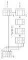
도 5는 본 발명에 따른 혼합 맵핑 동작을 사용하는 메모리 시스템을 보여주는 블록도이다. 도 5를 참조하면, 메모리 시스템(400)은 파일 시스템(410), 플래시 변환 레이어(420), 그리고 플래시 메모리(430)를 포함한다.5 is a block diagram illustrating a memory system using a mixed mapping operation according to the present invention. Referring to FIG. 5, the
플래시 변환 레이어(420)는 파일 시스템(410)으로부터 논리적 섹터 번호(LSN)를 입력받고, 맵핑 테이블을 사용하여 논리적 섹터 번호(LSN)를 물리적 섹터 번호(PSN)로 변환한다. 플래시 변환 레이어(420)는 물리적 섹터 번호(PSN)를 플래시 메모리(430)로 제공한다.The
도 5를 참조하면, 플래시 변환 레이어(420)는 블록 맵핑 테이블(421) 이외에, 랩-어라운드 페이지 맵핑 테이블(422)과 랜덤 페이지 맵핑 테이블(423)을 더 포함한다. 여기에서, 랜덤 페이지 맵핑 테이블(423)은 임의 위치 방식(out-of-place order) 방식에 따른 페이지 변환을 지정한 것이다. 랜덤 페이지 맵핑 테이블(423)은 도 6을 참조하여 상세히 설명된다.5, in addition to the block mapping table 421, the
랩-어라운드 페이지 맵핑 테이블(422)은 랩-어라운드 방식(wrap-around order)에 따른 페이지 변환을 지정한 것이다. 여기에서, 랩-어라운드 방식(wrap- around order)이란 페이지 위치 순서가 순차적으로 증가하되, 시작 페이지가 0번이 아닌 것을 의미한다. 예를 들어, 하나의 블록이 4개의 페이지로 구성되어 있다면, 랩-어라운드 방식(wrap-around order)에는 다음과 같은 경우가 있다.The wrap-around page mapping table 422 specifies page conversions in a wrap-around order. In this case, the wrap-around order means that the page position order is sequentially increased, but the start page is not zero. For example, if a block is composed of four pages, a wrap-around order may be as follows.
1) 1번 페이지 -> 2번 페이지 -> 3번 페이지 -> 0번 페이지1) Page 1-> Page 2-> Page 3->
2) 2번 페이지 -> 3번 페이지 -> 0번 페이지 -> 1번 페이지2) Page 2-> Page 3-> Page 0->
3) 3번 페이지 -> 0번 페이지 -> 1번 페이지 -> 2번 페이지3) Page 3-> Page 0-> Page 1->
랩-어라운드 방식(wrap-around order)은 순차 위치 방식(in-place order)과 마찬가지로 순차적으로 쓰여 진다. 다만, 시작 페이지가 0번 페이지가 아닐 따름이다. 도 3 및 도 4에 도시된 혼합 맵핑 방법에서는 랩-어라운드 방식(wrap-around order)의 경우에도 임의 위치 방식(out-of-place order)과 마찬가지로 처리된다. 즉, 도 4에 도시된 바와 같이, 4번의 페이지 복사와 2번의 블록 소거 동작이 수행된다.The wrap-around order is written sequentially, just like the in-place order. However, the start page is not
그러나 본 발명에 따른 메모리 시스템(400)은 랩-어라운드 페이지 맵핑 테이블(422)을 구비함으로, 랩-어라운드 방식(wrap-around order)을 순차 위치 방식(in-place order)처럼 처리한다. 본 발명에 의하면, 도 4의 예에서, 1번의 페이지 복사와 1번의 블록 소거 동작이 수행된다. 이는 도 7을 참조하여 상세히 설명된다.However, the
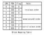
도 6은 도 5에 도시된 메모리 시스템의 맵핑 테이블 관리 방법을 예시적으로 보여주는 도표이다. 도 6(a)는 블록 맵핑 테이블, 도 6(b)는 랩-어라운드 페이지 맵핑 테이블, 도 6(c)는 랜덤 페이지 맵핑 테이블, 그리고 도 6(d)는 물리적 블록 의 페이지 위치를 보여준다.FIG. 6 is a diagram exemplarily illustrating a method of managing a mapping table of the memory system illustrated in FIG. 5. 6 (a) shows a block mapping table, FIG. 6 (b) shows a wrap-around page mapping table, FIG. 6 (c) shows a random page mapping table, and FIG. 6 (d) shows page positions of a physical block.
도 6(a)를 참조하면, 블록 맵핑 테이블은 논리적 블록 번호(Logical Block Number; LBN), 물리적 블록 번호(Physical Block Number; PBN), 플래그 정보를 갖는다. 도 6(a)에서 참고(Note)에는 플래그 정보에 따른 페이지 위치 방식이 도시되어 있다.Referring to FIG. 6A, the block mapping table has a logical block number (LBN), a physical block number (PBN), and flag information. In FIG. 6 (a), note shows a page position method according to flag information.
플래그(Flag) 0은 순차 위치 방식(in-place order)을 뜻한다. 플래그(Flag) 1은 랩-어라운드 방식(wrap-around order)을 뜻한다. 그리고 플래그(Flag) 2는 임의 위치 방식(out-of-place order)을 뜻한다. 즉, 블록 맵핑 테이블은 페이지 위치 방식을 정의한 플래그 정보를 갖는다.
여기에서, 순차 위치 방식(in-place order)은 0번 페이지부터 시작하기 때문에, 오프셋(offset) 정보를 필요로 하지 않는다. 그러나 랩-어라운드 방식(wrap-around order)은 시작 페이지를 정의해 주어야 한다. 그리고 임의 위치 방식(out-of-place order)은 페이지 순서를 정의해 주어야 한다.Here, since the in-place order starts with
도 6(b)는 랩-어라운드 페이지 맵핑 테이블을 보여준다. 도 6(b)를 참조하면, 물리적 블록 번호 400은 오프셋 1을 갖는다. 이는 물리적 블록 번호 400의 시작 페이지가 1번 페이지임을 뜻한다. 물리적 블록 번호 500은 오프셋 2를 갖는다. 이는 물리적 블록 번호 500의 시작 페이지가 2번 페이지임을 뜻한다. 즉, 물리적 블록 번호 500의 제 1 물리적 페이지에는 2번 논리적 페이지가 쓰여 진다. 물리적 블록 번호 600은 오프셋 3을 갖는다. 이는 물리적 블록 번호 600의 시작 페이지가 3번 페이지임을 뜻한다. 물리적 블록 번호 400 내지 600의 페이지 위치는 도 6(d) 에 구체적으로 도시되어 있다.6 (b) shows a wrap-around page mapping table. Referring to FIG. 6B, the
도 6(c) 랜덤 페이지 맵핑 테이블을 보여준다. 랜덤 페이지 맵핑 테이블에는 임의 위치 방식(out-of-place order)에 따른 페이지 순서가 정의되어 있다. 도 6(c)를 참조하면, 물리적 블록 번호(PBN) 700에 대한 오프셋 정보는 0, 3, 2, 1이다. 따라서 물리적 블록 번호(PBN) 700의 제 1 내지 제 4 물리적 페이지에는 0번, 3번, 2번, 1번 페이지가 쓰여 진다. 물리적 블록 번호(PBN) 800에 대한 오프셋 정보는 1, 3, 2, 0이다. 따라서 물리적 블록 번호(PBN) 800의 제 1 내지 제 4 물리적 페이지에는 1번, 3번, 2번, 0번 페이지가 쓰여 진다. 물리적 블록 번호 700 및 800의 페이지 위치는 도 6(d)에 구체적으로 도시되어 있다.6 (c) shows a random page mapping table. In the random page mapping table, a page order according to an out-of-place order is defined. Referring to FIG. 6C, offset information for the physical
이하에서는 도 6에 도시된 맵핑 테이블을 참조하여, 페이지 읽기 동작이 설명된다.Hereinafter, a page read operation will be described with reference to the mapping table illustrated in FIG. 6.
먼저, 1번 블록의 2번 페이지에 대한 페이지 읽기 동작이 설명된다. 플래시 변환 레이어(FTL)는 블록 맵핑 테이블을 참조하여, 1번 논리적 블록 번호(LBN)에 대응하는 200번 물리적 블록 번호(PBN)를 찾는다. 플래시 변환 레이어(FTL)는 플래그 정보를 확인한다. 도 6(a)에서, 1번 논리적 블록 번호(LBN)에 대응하는 플래그(Flag)는 0이다. 이것은 200번 물리적 블록 번호(PBN)는 순차 위치 방식(in-place order)에 따라 페이지가 배열되어 있음을 뜻한다. 따라서 200번 물리적 블록 번호(PBN)의 1번 페이지가 읽혀진다.First, a page read operation for
다음으로, 4번 블록의 2번 페이지에 대한 페이지 읽기 동작이 설명된다. 플래시 변환 레이어(FTL)는 블록 맵핑 테이블을 참조하여, 4번 논리적 블록 번 호(LBN)에 대응하는 500번 물리적 블록 번호(PBN)를 찾는다. 플래시 변환 레이어(FTL)은 4번 논리적 블록 번호(LBN)에 대응하는 플래그(Flag) 1을 확인한다. 이것은 500번 물리적 블록 번호(PBN)는 랩-어라운드 방식(wrap-around order)에 따라 페이지가 배열되어 있음을 뜻한다.Next, a page read operation for
플래시 변환 레이어(FTL)는 도 6(b)에 도시되어 있는 랩-어라운드 페이지 맵핑 테이블을 참조한다. 도 6(b)를 참조하면, 500번 물리적 블록 번호(PBN)에 대한 오프셋 정보는 2이다. 따라서 500번 물리적 블록 번호(PBN)에는 2번, 3번, 0번, 1번 페이지 순서로 배열되어 있다. 따라서 500번 물리적 블록 번호(PBN)에 있는 3번 페이지가 읽혀진다.The flash translation layer FTL refers to the wrap-around page mapping table shown in FIG. 6 (b). Referring to FIG. 6 (b), the offset information for physical block number 500 (PBN) is two. Therefore, the 500 physical block number (PBN) is arranged in the order of
마지막으로, 6번 블록의 2번 페이지에 대한 읽기 동작이 설명된다. 플래시 변환 레이어(FTL)는 블록 맵핑 테이블을 참조하여, 6번 논리적 블록 번호(LBN)에 대응하는 700번 물리적 블록 번호(PBN)를 찾는다. 플래시 변환 레이어(FTL)는 6번 논리적 블록 번호(LBN)에 대응하는 플래그(Flag) 2를 확인한다. 이것은 700번 물리적 블록 번호(PBN)는 임의 위치 방식(out-of-place order)에 따라 페이지가 배열되어 있음을 뜻한다.Finally, the read operation for
플래시 변환 레이어(FTL)는 도 6(c)에 도시되어 있는 랜덤 페이지 맵핑 테이블을 참조한다. 도 6(c)를 참조하면, 700번 물리적 블록 번호(PBN)에 대한 오프셋 정보는 0, 3, 2, 1이다. 따라서 700번 물리적 블록 번호(PBN)에는 0번, 3번, 2번, 1번 페이지 순서로 배열되어 있다. 따라서 700번 물리적 블록 번호(PBN)에 있는 3번 페이지가 읽혀진다.The flash translation layer FTL refers to the random page mapping table illustrated in FIG. 6C. Referring to FIG. 6C, offset information for physical block number 700 (PBN) is 0, 3, 2, and 1. Therefore, the
도 6(d)에는 각각의 물리적 블록 번호에 대한 페이지 위치 방식이 도시되어 있다. 물리적 블록 번호(PBN) 100 내지 300은 플래그(Flag) 0이므로, 순차 위치 방식(in-place order)따라 페이지가 배열되어 있다. 물리적 블록 번호(PBN) 400 내지 600은 플래그(Flag) 1이므로, 랩-어라운드 방식(wrap-around order)에 따라 페이지가 배열되어 있다. 그리고 물리적 블록 번호(PBN) 700 및 800은 플래그(Flag) 2이므로, 임의 위치 방식(out-of-place order)에 따라 페이지가 배열되어 있다.In FIG. 6 (d), the page position method for each physical block number is shown. Since the physical
도 7은 도 5에 도시된 메모리 시스템의 혼합 맵핑 동작을 예시적으로 설명하기 위한 다이어그램이다. 도 4에 도시된 맵핑 방법에 의하면, 4번의 페이지 복사와 2번의 블록 소거 동작이 수행된다. 그러나 도 7에 도시된 맵핑 방법에 의하면, 1번의 페이지 복수와 1번의 블록 소거 동작이 수행된다.FIG. 7 is a diagram for exemplarily describing a mixed mapping operation of the memory system illustrated in FIG. 5. According to the mapping method illustrated in FIG. 4, four page copies and two block erase operations are performed. However, according to the mapping method illustrated in FIG. 7, one page plural and one block erase operation are performed.
도 7에 도시된 바와 같이, 로그 블록(510)의 제 1 내지 제 3 물리적 페이지에는 2번, 3번, 0번 페이지가 쓰여져 있고, 데이터 블록(520)의 제 2 물리적 페이지에는 1번 페이지가 쓰여져 있다. 여기에서, 페이지 위치 순서가 2번, 3번, 0번, 1번이면, 랩-어라운드 방식(wrap-around order)이 된다.As shown in FIG. 7,
이러한 경우에, 본 발명에서는 데이터 블록(520)의 제 2 물리적 페이지에 저장된 1번 페이지가 로그 블록(510)의 제 4 번 물리적 페이지에 복사된다. 그리고 로그 블록(510)은 새로운 데이터 블록으로 등록된다. 로그 블록(510)은 블록 맵핑 테이블 및 랩-어라운드 페이지 맵핑 테이블에, 플래그 1, 오프셋 2를 갖는 새로운 데이터 블록으로 등록된다. 데이터 블록(520)은 소거된다. 따라서, 도 5에 도시된 메모리 시스템(400)은 한 번의 페이지 복사와 1번의 블록 소거 동작을 수행한다.In this case, in the present invention, the first page stored in the second physical page of the data block 520 is copied to the fourth physical page of the
한편, 본 발명에 따른 메모리 시스템은 메모리의 공간이 충분할 경우에는 랜덤 페이지 맵핑 테이블을 추가할 수도 있다. 본 발명에 따른 메모리 시스템은 랩-어라운드 방식(wrap-around order)을 순차 위치 방식(in-place order)과 동일하게 처리한다. 본 발명에 의하면, 머지 연산에 필요한 페이지 복수 횟수 및 블록 소거 횟수를 크게 줄일 수 있다.Meanwhile, the memory system according to the present invention may add a random page mapping table when there is sufficient space in the memory. The memory system according to the present invention treats the wrap-around order in the same way as the in-place order. According to the present invention, the number of page plurals and the number of block erases required for a merge operation can be greatly reduced.
본 발명은 플래그 정보 및 오프셋 정보를 참조하여 읽기 동작을 수행하기 때문에, 도 4에 도시된 것처럼 페이지 순서를 맞출 필요가 없다. 본 발명에 의하면, 페이지 복사 횟수와 블록 소거 횟수가 줄어들기 때문에 메모리 시스템의 성능이 크게 향상된다.Since the present invention performs the read operation with reference to the flag information and the offset information, it is not necessary to adjust the page order as shown in FIG. According to the present invention, since the number of page copies and the number of block erases are reduced, the performance of the memory system is greatly improved.
또한, 블록 맵핑 테이블은 플래그 정보를 기록하기 위해 2비트 정도의 메모리 공간만을 더 필요로 한다. 또한, 랩-어라운드 페이지 맵핑 테이블은 오프셋 정보를 기록하기 위해 1비트 내지 2비트 정도의 메모리 공간만을 필요로 한다. 따라서 본 발명에 따른 메모리 시스템 및 그것의 맵핑 테이블 관리 방법은 메모리의 공간을 크게 늘리지 않으면서, 페이지 복사 횟수 및 블록 소거 횟수를 크게 줄일 수 있다.In addition, the block mapping table needs only 2 bits of memory space to record the flag information. In addition, the wrap-around page mapping table only needs about 1 to 2 bits of memory space to record offset information. Therefore, the memory system and its mapping table management method according to the present invention can greatly reduce the number of page copies and the number of block erases without significantly increasing the space of the memory.
한편, 본 발명의 상세한 설명에서는 구체적인 실시예에 관하여 설명하였으나, 본 발명의 범위에서 벗어나지 않는 한도 내에서 여러 가지 변형이 가능함은 물론이다. 그러므로 본 발명의 범위는 상술한 실시예에 국한되어 정해져서는 안되며 후술하는 특허청구범위 뿐만 아니라 이 발명의 특허청구범위와 균등한 것들에 의해 정해져야 한다.On the other hand, in the detailed description of the present invention has been described with respect to specific embodiments, various modifications are of course possible without departing from the scope of the invention. Therefore, the scope of the present invention should not be limited to the above-described embodiments, but should be defined by the equivalents of the claims of the present invention as well as the following claims.
이상에서 살펴본 바와 같이, 본 발명에 따른 메모리 시스템 및 그것의 맵핑 테이블 관리 방법에 의하면, 메모리의 공간을 크게 늘리지 않으면서, 페이지 복사 횟수 및 블록 소거 횟수를 크게 줄일 수 있다.As described above, according to the memory system and the mapping table managing method thereof according to the present invention, the number of page copies and the number of block erases can be greatly reduced without greatly increasing the memory space.
Claims (16)
Translated fromKoreanPriority Applications (2)
| Application Number | Priority Date | Filing Date | Title |
|---|---|---|---|
| KR1020060101961AKR100806343B1 (en) | 2006-10-19 | 2006-10-19 | Memory system including flash memory and its mapping table management method |
| US11/637,792US20080098195A1 (en) | 2006-10-19 | 2006-12-13 | Memory system including flash memory and mapping table management method |
Applications Claiming Priority (1)
| Application Number | Priority Date | Filing Date | Title |
|---|---|---|---|
| KR1020060101961AKR100806343B1 (en) | 2006-10-19 | 2006-10-19 | Memory system including flash memory and its mapping table management method |
Publications (1)
| Publication Number | Publication Date |
|---|---|
| KR100806343B1true KR100806343B1 (en) | 2008-02-27 |
Family
ID=39319428
Family Applications (1)
| Application Number | Title | Priority Date | Filing Date |
|---|---|---|---|
| KR1020060101961AExpired - Fee RelatedKR100806343B1 (en) | 2006-10-19 | 2006-10-19 | Memory system including flash memory and its mapping table management method |
Country Status (2)
| Country | Link |
|---|---|
| US (1) | US20080098195A1 (en) |
| KR (1) | KR100806343B1 (en) |
Cited By (8)
| Publication number | Priority date | Publication date | Assignee | Title |
|---|---|---|---|---|
| US8027194B2 (en) | 1988-06-13 | 2011-09-27 | Samsung Electronics Co., Ltd. | Memory system and method of accessing a semiconductor memory device |
| KR101103210B1 (en)* | 2008-05-05 | 2012-01-05 | 인텔 코포레이션 | Sequence Number Wrap-Around Devices, Methods, and Articles |
| US8239616B2 (en) | 2008-12-03 | 2012-08-07 | Samsung Electronics Co., Ltd. | Semiconductor device comprising flash memory and address mapping method |
| KR101570179B1 (en) | 2008-12-08 | 2015-11-18 | 삼성전자주식회사 | - Cache synchronization method and system for fast power-off |
| KR101923661B1 (en) | 2016-04-04 | 2018-11-29 | 주식회사 맴레이 | Flash-based accelerator and computing device including the same |
| CN113093997A (en)* | 2021-04-19 | 2021-07-09 | 深圳市安信达存储技术有限公司 | Method for separating data Based on Host-Based FTL (fiber to the Home) architecture |
| KR20230103000A (en)* | 2021-12-30 | 2023-07-07 | 중앙대학교 산학협력단 | Memory system and method for managing i/o of memory system and computing device for executing the method |
| US11762576B2 (en) | 2020-08-28 | 2023-09-19 | SK Hynix Inc. | Semiconductor memory device and operating method for repairing guarantee blocks |
Families Citing this family (50)
| Publication number | Priority date | Publication date | Assignee | Title |
|---|---|---|---|---|
| US7984084B2 (en)* | 2005-08-03 | 2011-07-19 | SanDisk Technologies, Inc. | Non-volatile memory with scheduled reclaim operations |
| US7739444B2 (en)* | 2006-12-26 | 2010-06-15 | Sandisk Corporation | System using a direct data file system with a continuous logical address space interface |
| US8046522B2 (en)* | 2006-12-26 | 2011-10-25 | SanDisk Technologies, Inc. | Use of a direct data file system with a continuous logical address space interface and control of file address storage in logical blocks |
| KR101473344B1 (en)* | 2007-08-24 | 2014-12-17 | 삼성전자 주식회사 | Devices that use flash memory as storage and how they work |
| US8239875B2 (en)* | 2007-12-21 | 2012-08-07 | Spansion Llc | Command queuing for next operations of memory devices |
| US7949851B2 (en)* | 2007-12-28 | 2011-05-24 | Spansion Llc | Translation management of logical block addresses and physical block addresses |
| KR101465789B1 (en)* | 2008-01-24 | 2014-11-26 | 삼성전자주식회사 | Write and merge methods in memory card systems for reducing the number of page copies |
| KR101477047B1 (en) | 2008-02-29 | 2014-12-30 | 삼성전자주식회사 | Memory system and its block merging method |
| US8464021B2 (en)* | 2008-05-28 | 2013-06-11 | Spansion Llc | Address caching stored translation |
| KR101086857B1 (en)* | 2008-07-25 | 2011-11-25 | 주식회사 팍스디스크 | Control Method of Semiconductor Storage System Performing Data Merge |
| US8838876B2 (en) | 2008-10-13 | 2014-09-16 | Micron Technology, Inc. | Translation layer in a solid state storage device |
| KR101028929B1 (en)* | 2008-12-31 | 2011-04-12 | 성균관대학교산학협력단 | Log block association distribution method for real-time system and flash memory device |
| US8364931B2 (en)* | 2009-06-29 | 2013-01-29 | Mediatek Inc. | Memory system and mapping methods using a random write page mapping table |
| US8443167B1 (en) | 2009-12-16 | 2013-05-14 | Western Digital Technologies, Inc. | Data storage device employing a run-length mapping table and a single address mapping table |
| US8194340B1 (en) | 2010-03-18 | 2012-06-05 | Western Digital Technologies, Inc. | Disk drive framing write data with in-line mapping data during write operations |
| US8693133B1 (en) | 2010-03-22 | 2014-04-08 | Western Digital Technologies, Inc. | Systems and methods for improving sequential data rate performance using sorted data zones for butterfly format |
| US8687306B1 (en) | 2010-03-22 | 2014-04-01 | Western Digital Technologies, Inc. | Systems and methods for improving sequential data rate performance using sorted data zones |
| US9330715B1 (en) | 2010-03-22 | 2016-05-03 | Western Digital Technologies, Inc. | Mapping of shingled magnetic recording media |
| US8856438B1 (en) | 2011-12-09 | 2014-10-07 | Western Digital Technologies, Inc. | Disk drive with reduced-size translation table |
| US8699185B1 (en) | 2012-12-10 | 2014-04-15 | Western Digital Technologies, Inc. | Disk drive defining guard bands to support zone sequentiality when butterfly writing shingled data tracks |
| US8667248B1 (en) | 2010-08-31 | 2014-03-04 | Western Digital Technologies, Inc. | Data storage device using metadata and mapping table to identify valid user data on non-volatile media |
| US8954664B1 (en) | 2010-10-01 | 2015-02-10 | Western Digital Technologies, Inc. | Writing metadata files on a disk |
| US8756361B1 (en) | 2010-10-01 | 2014-06-17 | Western Digital Technologies, Inc. | Disk drive modifying metadata cached in a circular buffer when a write operation is aborted |
| KR101739556B1 (en)* | 2010-11-15 | 2017-05-24 | 삼성전자주식회사 | Data storage device, user device and data write method thereof |
| US8793429B1 (en) | 2011-06-03 | 2014-07-29 | Western Digital Technologies, Inc. | Solid-state drive with reduced power up time |
| US8924629B1 (en) | 2011-06-07 | 2014-12-30 | Western Digital Technologies, Inc. | Mapping table for improving write operation efficiency |
| US8756382B1 (en) | 2011-06-30 | 2014-06-17 | Western Digital Technologies, Inc. | Method for file based shingled data storage utilizing multiple media types |
| US9213493B1 (en) | 2011-12-16 | 2015-12-15 | Western Digital Technologies, Inc. | Sorted serpentine mapping for storage drives |
| US8819367B1 (en) | 2011-12-19 | 2014-08-26 | Western Digital Technologies, Inc. | Accelerated translation power recovery |
| US8612706B1 (en) | 2011-12-21 | 2013-12-17 | Western Digital Technologies, Inc. | Metadata recovery in a disk drive |
| KR20130084846A (en)* | 2012-01-18 | 2013-07-26 | 삼성전자주식회사 | Storage device based on a flash memory, user device including the same, and data read method thereof |
| US8984247B1 (en) | 2012-05-10 | 2015-03-17 | Western Digital Technologies, Inc. | Storing and reconstructing mapping table data in a data storage system |
| US8966205B1 (en) | 2012-05-10 | 2015-02-24 | Western Digital Technologies, Inc. | System data management using garbage collection and hybrid self mapping |
| US9977612B1 (en) | 2012-05-11 | 2018-05-22 | Western Digital Technologies, Inc. | System data management using garbage collection and logs |
| US9170932B1 (en) | 2012-05-22 | 2015-10-27 | Western Digital Technologies, Inc. | System data storage mechanism providing coherency and segmented data loading |
| WO2014123372A1 (en)* | 2013-02-07 | 2014-08-14 | 서울대학교 산학협력단 | Flash translation layer design framework for provable and accurate error recovery |
| US10176048B2 (en) | 2014-02-07 | 2019-01-08 | International Business Machines Corporation | Creating a restore copy from a copy of source data in a repository having source data at different point-in-times and reading data from the repository for the restore copy |
| US11194667B2 (en) | 2014-02-07 | 2021-12-07 | International Business Machines Corporation | Creating a restore copy from a copy of a full copy of source data in a repository that is at a different point-in-time than a restore point-in-time of a restore request |
| US11169958B2 (en) | 2014-02-07 | 2021-11-09 | International Business Machines Corporation | Using a repository having a full copy of source data and point-in-time information from point-in-time copies of the source data to restore the source data at different points-in-time |
| US10372546B2 (en) | 2014-02-07 | 2019-08-06 | International Business Machines Corporation | Creating a restore copy from a copy of source data in a repository having source data at different point-in-times |
| US10387446B2 (en) | 2014-04-28 | 2019-08-20 | International Business Machines Corporation | Merging multiple point-in-time copies into a merged point-in-time copy |
| KR20150139718A (en)* | 2014-06-03 | 2015-12-14 | 에스케이하이닉스 주식회사 | Controller for controlling nonvolatile memory and semiconductor device including the same |
| US8953269B1 (en) | 2014-07-18 | 2015-02-10 | Western Digital Technologies, Inc. | Management of data objects in a data object zone |
| US9875055B1 (en) | 2014-08-04 | 2018-01-23 | Western Digital Technologies, Inc. | Check-pointing of metadata |
| TWI512609B (en) | 2014-09-05 | 2015-12-11 | Silicon Motion Inc | Methods for scheduling read commands and apparatuses using the same |
| KR20160070920A (en)* | 2014-12-10 | 2016-06-21 | 에스케이하이닉스 주식회사 | Memory system including semiconductor memory device and controller having map table and operating method thereof |
| US10884947B2 (en) | 2017-11-17 | 2021-01-05 | SK Hynix Inc. | Methods and memory systems for address mapping |
| CN109800178B (en)* | 2017-11-17 | 2023-05-16 | 爱思开海力士有限公司 | Garbage collection method and memory system for hybrid address mapping |
| CN108062203B (en)* | 2017-12-15 | 2021-02-26 | 北京兆易创新科技股份有限公司 | Flash memory data management method and device and memory |
| CN118916302A (en) | 2019-06-21 | 2024-11-08 | 慧荣科技股份有限公司 | Flash memory physical resource set management device and method and computer readable storage medium |
Citations (5)
| Publication number | Priority date | Publication date | Assignee | Title |
|---|---|---|---|---|
| US5713005A (en) | 1995-02-10 | 1998-01-27 | Townsend And Townsend And Crew Llp | Method and apparatus for pipelining data in an integrated circuit |
| KR19990027320A (en)* | 1997-09-29 | 1999-04-15 | 윤종용 | Synchronous random access memory control device and method |
| JP2000105694A (en) | 1998-09-28 | 2000-04-11 | Nec Ic Microcomput Syst Ltd | Flash memory, microcomputer equipped with flash memory, and method for storing program in flash memory |
| KR20020075291A (en)* | 2001-03-22 | 2002-10-04 | 마쯔시다덴기산교 가부시키가이샤 | Storage device |
| KR20050070672A (en)* | 2003-12-30 | 2005-07-07 | 삼성전자주식회사 | Method for address mapping and managing mapping information, and flash memory thereof |
Family Cites Families (3)
| Publication number | Priority date | Publication date | Assignee | Title |
|---|---|---|---|---|
| US6678785B2 (en)* | 2001-09-28 | 2004-01-13 | M-Systems Flash Disk Pioneers Ltd. | Flash management system using only sequential write |
| US7254668B1 (en)* | 2002-10-28 | 2007-08-07 | Sandisk Corporation | Method and apparatus for grouping pages within a block |
| US7139864B2 (en)* | 2003-12-30 | 2006-11-21 | Sandisk Corporation | Non-volatile memory and method with block management system |
- 2006
- 2006-10-19KRKR1020060101961Apatent/KR100806343B1/ennot_activeExpired - Fee Related
- 2006-12-13USUS11/637,792patent/US20080098195A1/ennot_activeAbandoned
Patent Citations (5)
| Publication number | Priority date | Publication date | Assignee | Title |
|---|---|---|---|---|
| US5713005A (en) | 1995-02-10 | 1998-01-27 | Townsend And Townsend And Crew Llp | Method and apparatus for pipelining data in an integrated circuit |
| KR19990027320A (en)* | 1997-09-29 | 1999-04-15 | 윤종용 | Synchronous random access memory control device and method |
| JP2000105694A (en) | 1998-09-28 | 2000-04-11 | Nec Ic Microcomput Syst Ltd | Flash memory, microcomputer equipped with flash memory, and method for storing program in flash memory |
| KR20020075291A (en)* | 2001-03-22 | 2002-10-04 | 마쯔시다덴기산교 가부시키가이샤 | Storage device |
| KR20050070672A (en)* | 2003-12-30 | 2005-07-07 | 삼성전자주식회사 | Method for address mapping and managing mapping information, and flash memory thereof |
Cited By (18)
| Publication number | Priority date | Publication date | Assignee | Title |
|---|---|---|---|---|
| US8027194B2 (en) | 1988-06-13 | 2011-09-27 | Samsung Electronics Co., Ltd. | Memory system and method of accessing a semiconductor memory device |
| KR101103210B1 (en)* | 2008-05-05 | 2012-01-05 | 인텔 코포레이션 | Sequence Number Wrap-Around Devices, Methods, and Articles |
| US8171205B2 (en) | 2008-05-05 | 2012-05-01 | Intel Corporation | Wrap-around sequence numbers for recovering from power-fall in non-volatile memory |
| US8705272B2 (en) | 2008-06-13 | 2014-04-22 | Samsung Electronics Co., Ltd. | Memory system and method of accessing a semiconductor memory device |
| US8565021B2 (en) | 2008-06-13 | 2013-10-22 | Samsung Electronics Co., Ltd. | Memory system and method of accessing a semiconductor memory device |
| US8614919B2 (en) | 2008-06-13 | 2013-12-24 | Samsung Electronics Co., Ltd. | Memory system and method of accessing a semiconductor memory device |
| US8625344B2 (en) | 2008-06-13 | 2014-01-07 | Samsung Electronics Co., Ltd. | Memory system and method of accessing a semiconductor memory device |
| US8638585B2 (en) | 2008-06-13 | 2014-01-28 | Samsung Electronics Co., Ltd. | Memory system and method of accessing a semiconductor memory device |
| US8760918B2 (en) | 2008-06-13 | 2014-06-24 | Samsung Electronics Co., Ltd. | Memory system and method of accessing a semiconductor memory device |
| US8239616B2 (en) | 2008-12-03 | 2012-08-07 | Samsung Electronics Co., Ltd. | Semiconductor device comprising flash memory and address mapping method |
| KR101570179B1 (en) | 2008-12-08 | 2015-11-18 | 삼성전자주식회사 | - Cache synchronization method and system for fast power-off |
| KR101923661B1 (en) | 2016-04-04 | 2018-11-29 | 주식회사 맴레이 | Flash-based accelerator and computing device including the same |
| US10824341B2 (en) | 2016-04-04 | 2020-11-03 | MemRay Corporation | Flash-based accelerator and computing device including the same |
| US10831376B2 (en) | 2016-04-04 | 2020-11-10 | MemRay Corporation | Flash-based accelerator and computing device including the same |
| US11762576B2 (en) | 2020-08-28 | 2023-09-19 | SK Hynix Inc. | Semiconductor memory device and operating method for repairing guarantee blocks |
| CN113093997A (en)* | 2021-04-19 | 2021-07-09 | 深圳市安信达存储技术有限公司 | Method for separating data Based on Host-Based FTL (fiber to the Home) architecture |
| KR20230103000A (en)* | 2021-12-30 | 2023-07-07 | 중앙대학교 산학협력단 | Memory system and method for managing i/o of memory system and computing device for executing the method |
| KR102812181B1 (en)* | 2021-12-30 | 2025-05-26 | 중앙대학교 산학협력단 | Memory system and method for managing i/o of memory system and computing device for executing the method |
Also Published As
| Publication number | Publication date |
|---|---|
| US20080098195A1 (en) | 2008-04-24 |
Similar Documents
| Publication | Publication Date | Title |
|---|---|---|
| KR100806343B1 (en) | Memory system including flash memory and its mapping table management method | |
| KR100885181B1 (en) | Memory system performing group mapping operation and address mapping method thereof | |
| US11232041B2 (en) | Memory addressing | |
| KR101465789B1 (en) | Write and merge methods in memory card systems for reducing the number of page copies | |
| KR101477047B1 (en) | Memory system and its block merging method | |
| US7702844B2 (en) | Address mapping method and mapping information managing method for flash memory, and flash memory using the same | |
| TWI782977B (en) | Memory system and operating method thereof | |
| US8341371B2 (en) | Method of managing copy operations in flash memories | |
| US8364931B2 (en) | Memory system and mapping methods using a random write page mapping table | |
| KR100771521B1 (en) | Flash memory device including multi-level cells and method of writing data thereof | |
| US7287117B2 (en) | Flash memory and mapping control apparatus and method for flash memory | |
| US20080120488A1 (en) | Apparatus and method of managing nonvolatile memory | |
| US20080082729A1 (en) | Device driver including a flash memory file system and method thereof and a flash memory device and method thereof | |
| US20140297921A1 (en) | Method of Partitioning Physical Block and Memory System Thereof | |
| KR20100042455A (en) | Flash memory system and method of flash translation layer design thereof | |
| WO2007066720A1 (en) | Nonvolatile memory device, method of writing data, and method of reading out data | |
| US20100287330A1 (en) | Method for writing data into flash memory | |
| KR100845552B1 (en) | FLT address mapping method | |
| US11113205B2 (en) | Die addressing using a reduced size translation table entry | |
| KR101119866B1 (en) | Flash memory comprising flexible size flash memory per partition and memory system using thereof | |
| KR20090046568A (en) | Flash memory system and its write method | |
| US20060224817A1 (en) | NOR flash file allocation | |
| JP2008299513A (en) | Data storage device, and method for controlling the same | |
| KR100688463B1 (en) | How to record and delete data in physical memory | |
| KR20050102779A (en) | Design of nand flash memory file system |
Legal Events
| Date | Code | Title | Description |
|---|---|---|---|
| A201 | Request for examination | ||
| PA0109 | Patent application | St.27 status event code:A-0-1-A10-A12-nap-PA0109 | |
| PA0201 | Request for examination | St.27 status event code:A-1-2-D10-D11-exm-PA0201 | |
| P11-X000 | Amendment of application requested | St.27 status event code:A-2-2-P10-P11-nap-X000 | |
| P13-X000 | Application amended | St.27 status event code:A-2-2-P10-P13-nap-X000 | |
| R15-X000 | Change to inventor requested | St.27 status event code:A-3-3-R10-R15-oth-X000 | |
| R16-X000 | Change to inventor recorded | St.27 status event code:A-3-3-R10-R16-oth-X000 | |
| D13-X000 | Search requested | St.27 status event code:A-1-2-D10-D13-srh-X000 | |
| D14-X000 | Search report completed | St.27 status event code:A-1-2-D10-D14-srh-X000 | |
| E701 | Decision to grant or registration of patent right | ||
| PE0701 | Decision of registration | St.27 status event code:A-1-2-D10-D22-exm-PE0701 | |
| GRNT | Written decision to grant | ||
| PR0701 | Registration of establishment | St.27 status event code:A-2-4-F10-F11-exm-PR0701 | |
| PR1002 | Payment of registration fee | St.27 status event code:A-2-2-U10-U11-oth-PR1002 Fee payment year number:1 | |
| PG1601 | Publication of registration | St.27 status event code:A-4-4-Q10-Q13-nap-PG1601 | |
| PR1001 | Payment of annual fee | St.27 status event code:A-4-4-U10-U11-oth-PR1001 Fee payment year number:4 | |
| PR1001 | Payment of annual fee | St.27 status event code:A-4-4-U10-U11-oth-PR1001 Fee payment year number:5 | |
| R18-X000 | Changes to party contact information recorded | St.27 status event code:A-5-5-R10-R18-oth-X000 | |
| FPAY | Annual fee payment | Payment date:20130131 Year of fee payment:6 | |
| PR1001 | Payment of annual fee | St.27 status event code:A-4-4-U10-U11-oth-PR1001 Fee payment year number:6 | |
| FPAY | Annual fee payment | Payment date:20140129 Year of fee payment:7 | |
| PR1001 | Payment of annual fee | St.27 status event code:A-4-4-U10-U11-oth-PR1001 Fee payment year number:7 | |
| LAPS | Lapse due to unpaid annual fee | ||
| PC1903 | Unpaid annual fee | St.27 status event code:A-4-4-U10-U13-oth-PC1903 Not in force date:20150216 Payment event data comment text:Termination Category : DEFAULT_OF_REGISTRATION_FEE | |
| PC1903 | Unpaid annual fee | St.27 status event code:N-4-6-H10-H13-oth-PC1903 Ip right cessation event data comment text:Termination Category : DEFAULT_OF_REGISTRATION_FEE Not in force date:20150216 |