KR100805124B1 - Manufacturing Method of Display Device and Display Device - Google Patents
Manufacturing Method of Display Device and Display DeviceDownload PDFInfo
- Publication number
- KR100805124B1 KR100805124B1KR1020070021503AKR20070021503AKR100805124B1KR 100805124 B1KR100805124 B1KR 100805124B1KR 1020070021503 AKR1020070021503 AKR 1020070021503AKR 20070021503 AKR20070021503 AKR 20070021503AKR 100805124 B1KR100805124 B1KR 100805124B1
- Authority
- KR
- South Korea
- Prior art keywords
- pad
- electrode
- display device
- forming
- layer
- Prior art date
- Legal status (The legal status is an assumption and is not a legal conclusion. Google has not performed a legal analysis and makes no representation as to the accuracy of the status listed.)
- Active
Links
Images


Classifications
- H—ELECTRICITY
- H05—ELECTRIC TECHNIQUES NOT OTHERWISE PROVIDED FOR
- H05B—ELECTRIC HEATING; ELECTRIC LIGHT SOURCES NOT OTHERWISE PROVIDED FOR; CIRCUIT ARRANGEMENTS FOR ELECTRIC LIGHT SOURCES, IN GENERAL
- H05B33/00—Electroluminescent light sources
- H05B33/02—Details
- H05B33/06—Electrode terminals
- H—ELECTRICITY
- H10—SEMICONDUCTOR DEVICES; ELECTRIC SOLID-STATE DEVICES NOT OTHERWISE PROVIDED FOR
- H10K—ORGANIC ELECTRIC SOLID-STATE DEVICES
- H10K59/00—Integrated devices, or assemblies of multiple devices, comprising at least one organic light-emitting element covered by group H10K50/00
- H10K59/10—OLED displays
- H10K59/12—Active-matrix OLED [AMOLED] displays
- H10K59/131—Interconnections, e.g. wiring lines or terminals
- H—ELECTRICITY
- H05—ELECTRIC TECHNIQUES NOT OTHERWISE PROVIDED FOR
- H05B—ELECTRIC HEATING; ELECTRIC LIGHT SOURCES NOT OTHERWISE PROVIDED FOR; CIRCUIT ARRANGEMENTS FOR ELECTRIC LIGHT SOURCES, IN GENERAL
- H05B33/00—Electroluminescent light sources
- H05B33/10—Apparatus or processes specially adapted to the manufacture of electroluminescent light sources
- H—ELECTRICITY
- H05—ELECTRIC TECHNIQUES NOT OTHERWISE PROVIDED FOR
- H05B—ELECTRIC HEATING; ELECTRIC LIGHT SOURCES NOT OTHERWISE PROVIDED FOR; CIRCUIT ARRANGEMENTS FOR ELECTRIC LIGHT SOURCES, IN GENERAL
- H05B33/00—Electroluminescent light sources
- H05B33/12—Light sources with substantially two-dimensional radiating surfaces
- H05B33/26—Light sources with substantially two-dimensional radiating surfaces characterised by the composition or arrangement of the conductive material used as an electrode
- H—ELECTRICITY
- H10—SEMICONDUCTOR DEVICES; ELECTRIC SOLID-STATE DEVICES NOT OTHERWISE PROVIDED FOR
- H10K—ORGANIC ELECTRIC SOLID-STATE DEVICES
- H10K50/00—Organic light-emitting devices
- H10K50/80—Constructional details
- H10K50/805—Electrodes
- H10K50/81—Anodes
- H10K50/818—Reflective anodes, e.g. ITO combined with thick metallic layers
- H—ELECTRICITY
- H10—SEMICONDUCTOR DEVICES; ELECTRIC SOLID-STATE DEVICES NOT OTHERWISE PROVIDED FOR
- H10K—ORGANIC ELECTRIC SOLID-STATE DEVICES
- H10K59/00—Integrated devices, or assemblies of multiple devices, comprising at least one organic light-emitting element covered by group H10K50/00
- H10K59/80—Constructional details
- H10K59/805—Electrodes
- H10K59/8051—Anodes
- H10K59/80518—Reflective anodes, e.g. ITO combined with thick metallic layers
- H—ELECTRICITY
- H10—SEMICONDUCTOR DEVICES; ELECTRIC SOLID-STATE DEVICES NOT OTHERWISE PROVIDED FOR
- H10K—ORGANIC ELECTRIC SOLID-STATE DEVICES
- H10K71/00—Manufacture or treatment specially adapted for the organic devices covered by this subclass
- H—ELECTRICITY
- H10—SEMICONDUCTOR DEVICES; ELECTRIC SOLID-STATE DEVICES NOT OTHERWISE PROVIDED FOR
- H10K—ORGANIC ELECTRIC SOLID-STATE DEVICES
- H10K71/00—Manufacture or treatment specially adapted for the organic devices covered by this subclass
- H10K71/621—Providing a shape to conductive layers, e.g. patterning or selective deposition
Landscapes
- Engineering & Computer Science (AREA)
- Manufacturing & Machinery (AREA)
- Microelectronics & Electronic Packaging (AREA)
- Physics & Mathematics (AREA)
- Optics & Photonics (AREA)
- Electroluminescent Light Sources (AREA)
- Devices For Indicating Variable Information By Combining Individual Elements (AREA)
- Internal Circuitry In Semiconductor Integrated Circuit Devices (AREA)
- Thin Film Transistor (AREA)
Abstract
Description
Translated fromKorean도 1은 본 발명의 일 실시예에 따른 유기 발광 표시 장치의 사시도이다.1 is a perspective view of an organic light emitting diode display according to an exemplary embodiment of the present invention.
도 2a 내지 도 2g는 본 발명의 제1 실시예에 따른 유기 발광 표시 장치의 제조 방법을 나타낸 단면도들이다.2A to 2G are cross-sectional views illustrating a method of manufacturing an organic light emitting display device according to a first embodiment of the present invention.
도 3a 내지 도 3c는 본 발명의 제2 실시예에 따른 유기 발광 표시 장치의 제조 방법을 나타낸 단면도들이다.3A to 3C are cross-sectional views illustrating a method of manufacturing an organic light emitting diode display according to a second exemplary embodiment of the present invention.
본 발명은 표시 장치의 제조 방법에 관한 것으로서, 보다 상세하게는 패드 전극의 손상을 억제할 수 있는 유기 발광 표시 장치의 제조 방법에 관한 것이다.The present invention relates to a method of manufacturing a display device, and more particularly, to a method of manufacturing an organic light emitting display device capable of suppressing damage to a pad electrode.
표시 장치 중에 유기 발광 소자를 구동하여 영상을 표시하는 유기 발광 표시 장치가 있다. 유기 발광 소자는 정공 주입 전극인 애노드 전극과 유기 발광층 및 전자 주입 전극인 캐소드 전극을 포함한다. 애노드 전극과 캐소드 전극이 유기 발광층에 각각 정공과 전자를 주입하면, 유기 발광층 내부에 전자와 정공이 결합한 여기자(exciton)가 생성되고, 여기자가 여기 상태로부터 기저 상태로 떨어질 때 발생하는 에너지에 의해 발광이 이루어진다.There is an organic light emitting diode display that displays an image by driving an organic light emitting diode. The organic light emitting diode includes an anode electrode which is a hole injection electrode, an organic light emitting layer, and a cathode electrode which is an electron injection electrode. When the anode electrode and the cathode electrode inject holes and electrons into the organic light emitting layer, respectively, an exciton in which electrons and holes are combined is generated inside the organic light emitting layer, and light is emitted by energy generated when the exciton falls from the excited state to the ground state. This is done.
능동 구동형 유기 발광 표시 장치에서 통상 기판에는 실제 화상 표시가 이루어지는 화소 영역과, 화소 영역의 외곽으로 패드 영역이 형성되며, 패드 영역에 구비된 패드 전극들 위로 외부 모듈이 실장된다. 화소 영역에는 적색과 녹색 및 청색의 유기 발광 소자들이 매트릭스 형태로 배치되고, 각 유기 발광 소자마다 적어도 2개의 박막 트랜지스터(thin film transistor; TFT, 이하 'TFT'라 한다)가 구비되어 유기 발광 소자를 독립적으로 제어한다.In an active driving organic light emitting display device, a substrate includes a pixel region where actual image display is performed, a pad region is formed outside the pixel region, and an external module is mounted on pad electrodes provided in the pad region. In the pixel region, red, green, and blue organic light emitting diodes are arranged in a matrix form, and at least two thin film transistors (TFTs) are provided for each organic light emitting diode. Independently controlled
일반적으로 유기 발광 표시 장치를 제조하는 과정은, (1)기판 위에 액티브층, 게이트 전극, 소오스 전극, 및 드레인 전극을 포함하는 TFT를 형성하고, (2)TFT를 덮도록 평탄화막을 형성하고, (3)평탄화막 위에 드레인 전극과 연결되는 제1 화소 전극을 형성하고, (4)제1 화소 전극 위에 유기 발광층과 제2 화소 전극을 형성하는 단계들을 포함한다. 패드 전극들은 TFT를 형성하는 과정 중에 패드 영역에 형성된다. 패드 전극들은 하나 이상의 절연층으로 덮이며, 절연층에 형성된 개구부를 통해 기판 상에 노출된다.In general, the process of manufacturing an organic light emitting display device includes (1) forming a TFT including an active layer, a gate electrode, a source electrode, and a drain electrode on a substrate, (2) forming a planarization film to cover the TFT, and 3) forming a first pixel electrode connected to the drain electrode on the planarization layer, and (4) forming an organic emission layer and a second pixel electrode on the first pixel electrode. The pad electrodes are formed in the pad region during the process of forming the TFT. The pad electrodes are covered with one or more insulating layers and are exposed on the substrate through openings formed in the insulating layer.
그런데 전술한 제조 과정에서 제1 화소 전극을 형성할 때, 제1 화소 전극의 형성을 패드 전극들이 노출된 상태에서 진행하게 되므로, 제1 화소 전극 식각액에 의해 패드 전극들이 손상될 수 있다. 즉 패드 전극들이 제1 화소 전극 식각액에 의해 식각되는 물질로 형성된 경우, 제거되어야 할 제1 화소 전극 부위와 함께 패드 전극들이 식각되어 패드 전극들에 단선이 발생할 수 있다.However, when the first pixel electrode is formed in the above-described manufacturing process, since the formation of the first pixel electrode is performed while the pad electrodes are exposed, the pad electrodes may be damaged by the first pixel electrode etchant. That is, when the pad electrodes are formed of a material etched by the first pixel electrode etchant, the pad electrodes may be etched together with the first pixel electrode portion to be removed, thereby causing disconnection to the pad electrodes.
따라서 본 발명은 상기한 문제점을 해소하기 위한 것으로서, 본 발명은 패드 전극의 손상을 억제할 수 있는 표시 장치의 제조 방법을 제공하고자 한다.Accordingly, the present invention is to solve the above problems, the present invention is to provide a method of manufacturing a display device that can suppress the damage to the pad electrode.
본 발명의 일 실시예에 따른 표시 장치의 제조 방법은, 제1 기판 위의 화소 영역에 박막 트랜지스터를 형성함과 동시에 제1 기판 위의 패드 영역에 패드 전극을 형성하고, 박막 트랜지스터와 연결되는 제1 화소 전극과 패드 전극을 덮는 패드 보호층을 동시에 형성하고, 패드 보호층을 제거하여 패드 전극을 노출시키는 단계들을 포함한다.A method of manufacturing a display device according to an exemplary embodiment of the present invention may include forming a thin film transistor in a pixel region on a first substrate, forming a pad electrode in a pad region on a first substrate, and connecting the thin film transistor to a thin film transistor. Simultaneously forming a pad protective layer covering the one pixel electrode and the pad electrode, and removing the pad protective layer to expose the pad electrode.
제1 화소 전극은 Ag을 포함할 수 있다. 제1 화소 전극은 제1 투명 도전막과, Ag를 포함하는 반사막, 및 제2 투명 도전막을 포함할 수 있다.The first pixel electrode may include Ag. The first pixel electrode may include a first transparent conductive film, a reflective film containing Ag, and a second transparent conductive film.
제1 화소 전극 위에 유기 발광층과 제2 화소 전극을 추가로 형성할 수 있다. 그리고 패드 보호층을 제거하기 전, 제1 기판 위에 제2 기판을 접합시킬 수 있다. 패드 보호층은 습식 식각으로 제거할 수 있다.An organic emission layer and a second pixel electrode may be further formed on the first pixel electrode. And before removing the pad protective layer, the second substrate may be bonded onto the first substrate. The pad protective layer can be removed by wet etching.
박막 트랜지스터를 형성하는 단계는, 제1 기판 위에 액티브층과 게이트 절연막 및 게이트 전극을 순차적으로 형성하고, 게이트 전극을 덮도록 게이트 절연막 위에 층간 절연막을 형성하고, 층간 절연막 위에 소오스 전극과 드레인 전극을 형성하는 단계들을 포함할 수 있다.In the forming of the thin film transistor, an active layer, a gate insulating film, and a gate electrode are sequentially formed on the first substrate, an interlayer insulating film is formed on the gate insulating film so as to cover the gate electrode, and a source electrode and a drain electrode are formed on the interlayer insulating film. It may include the steps to.
게이트 전극과 패드 전극은 같은 물질로 동시에 형성할 수 있다. 이 경우, 패드 전극은 MoW, Al, Cr, 및 Al/Cr으로 이루어진 군에서 선택되는 어느 하나를 포함할 수 있다. 다른 한편으로, 소오스 전극과 드레인 전극 및 패드 전극은 같은 물질로 동시에 형성할 수 있다. 이 경우, 패드 전극은 Ti, Ti-합금, Ta, 및 Ta-합금 으로 이루어진 군에서 선택되는 어느 하나를 포함할 수 있다.The gate electrode and the pad electrode may be simultaneously formed of the same material. In this case, the pad electrode may include any one selected from the group consisting of MoW, Al, Cr, and Al / Cr. On the other hand, the source electrode, the drain electrode, and the pad electrode may be simultaneously formed of the same material. In this case, the pad electrode may include any one selected from the group consisting of Ti, Ti-alloy, Ta, and Ta-alloy.
이하, 첨부한 도면을 참고로 하여 본 발명의 실시예에 대하여 본 발명이 속하는 기술 분야에서 통상의 지식을 가진 자가 용이하게 실시할 수 있도록 상세히 설명한다. 본 발명은 여러 가지 상이한 형태로 구현될 수 있으며 여기에서 설명하는 실시예에 한정되지 않는다.Hereinafter, exemplary embodiments of the present invention will be described in detail with reference to the accompanying drawings so that those skilled in the art may easily implement the present invention. As those skilled in the art would realize, the described embodiments may be modified in various different ways, all without departing from the spirit or scope of the present invention.
이하의 실시예를 설명함에 있어서 층, 막 등의 부분이 다른 부분의 "상부"에 형성된다고 할 때, 이는 다른 부분의 "바로 위에"있는 경우 뿐만 아니라 그 중간에 또 다른 부분이 있는 경우도 포함한다.In describing the following embodiments, when a part such as a layer, a film, etc. is formed at the "top" of another part, this includes not only the case of "just above" the other part but also another part in the middle. do.
도 1은 본 발명의 일 실시예에 따른 표시 장치의 사시도로서, 일례로 유기 발광 표시 장치를 보여주고 있다.1 is a perspective view of a display device according to an embodiment of the present invention, which illustrates an organic light emitting display device as an example.
도 1을 참고하면, 유기 발광 표시 장치(100)는 제1 기판(12)과, 실런트(14)에 의해 제1 기판(12)에 접합되는 제2 기판(16)을 포함한다. 실런트(14) 내측으로 제1 기판(12)과 제2 기판(16)이 마주하는 부분에 실제 화상 표시가 이루어지는 화소 영역(A100)이 형성되고, 실런트(14) 외측으로 제1 기판(12)이 노출된 부분이 패드 영역(A110)이 된다. 제2 기판(16)은 흡습재(도시하지 않음)를 내장하고 있다.Referring to FIG. 1, the organic light
제1 기판(12)의 화소 영역(A100)에는 복수의 서브-픽셀들(18)이 매트릭스 형태로 배치되며, 화소 영역(A100) 외측에는 서브-픽셀들(18)을 구동하기 위한 스캔 드라이버(20)와 데이터 드라이버(22)가 위치한다.A plurality of
제1 기판(12)의 패드 영역(A110)에는 스캔 드라이버(20)와 데이터 드라이버(22)로 전기적 신호를 전달하기 위한 패드 전극들(24)이 위치한다. 패드 전극 들(24) 위에는 외부 모듈(칩 온 글라스(chip on glass; COG) 또는 연성 인쇄회로(flexible printed circuit; FPC) 필름 등, 도시하지 않음)이 실장된다.
서브-픽셀(18)은 발광 소자(L1)와 구동 회로부로 이루어진다. 발광 소자(L1)는 애노드 전극과 유기 발광층 및 캐소드 전극을 포함한다. 구동 회로부는 일례로 스위칭용 제1 박막 트랜지스터(이하, '제1 TFT'라 한다)(T1)와, 구동용 제2 박막 트랜지스터(이하, '제2 TFT'라 한다)(T2)와, 저장 캐패시터(Cst)를 포함할 수 있다. 서브-픽셀(18)의 구성은 전술한 예에 한정되지 않는다.The
제1 TFT(T1)는 스캔 라인(SL1)과 데이터 라인(DL1)에 연결되며, 스캔 라인(SL1)에 입력되는 스위칭 전압에 따라 데이터 라인(DL1)에서 입력되는 데이터 전압을 제2 TFT(T2)로 전송한다. 저장 캐패시터(Cst)는 제1 TFT(T1)와 전원 라인(VDD)에 연결되며, 제1 TFT(T1)로부터 전송받은 전압과 전원 라인(VDD)에 공급되는 전압의 차이에 해당하는 전압(Vgs)을 저장한다.The first TFT T1 is connected to the scan line SL1 and the data line DL1, and the second TFT T2 receives a data voltage input from the data line DL1 according to a switching voltage input to the scan line SL1. To send). The storage capacitor Cst is connected to the first TFT T1 and the power line VDD, and the voltage Vgs corresponding to the difference between the voltage received from the first TFT T1 and the voltage supplied to the power line VDD. Save).
제2 TFT(T2)는 전원 라인(VDD)와 저장 캐패시터(Cst)에 연결되어 저장 캐패시터(Cst)에 저장된 전압(Vgs)와 문턱 전압(Vth)의 차이의 제곱에 비례하는 출력 전류를 발광 소자(L1)로 공급하고, 발광 소자(L1)는 출력 전류에 의해 발광한다.The second TFT T2 is connected to the power supply line VDD and the storage capacitor Cst to emit an output current that is proportional to the square of the difference between the voltage Vgs and the threshold voltage Vth stored in the storage capacitor Cst. It supplies to (L1), and the light emitting element L1 emits light by an output current.
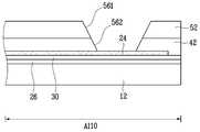
이하, 도 2a 내지 도 2g를 참고하여 본 발명의 제1 실시예에 따른 유기 발광 표시 장치의 제조 방법에 대해 설명한다. 도 2a 내지 도 2f는 유기 발광 표시 장치에서 화소 영역의 서브-픽셀과 패드 영역의 패드 전극을 나타내고 있으며, 화소 영역의 서브-픽셀에 대해서는 전술한 제1 TFT와 제2 TFT 가운데 제2 TFT만을 도시하고 있다. 도 2g는 패드 영역의 패드 전극만 선택적으로 나타내고 있다.Hereinafter, a method of manufacturing an organic light emitting display device according to a first exemplary embodiment of the present invention will be described with reference to FIGS. 2A to 2G. 2A to 2F illustrate a sub-pixel of a pixel area and a pad electrode of a pad area in an organic light emitting diode display, and only a second TFT among the above-described first and second TFTs is illustrated for a sub-pixel of a pixel area. Doing. 2G selectively shows only pad electrodes in the pad region.
도 2a를 참고하면, 화소 영역(A100)과 패드 영역(A110)을 포함하는 제1 기판(12)의 전면(全面)에 버퍼층(26)을 형성한다. 버퍼층(26)은 제1 기판(12)으로부터 유출되는 불순물로부터 후속 공정에서 형성되는 TFT를 보호하며, 실리콘 질화물 단독 또는 실리콘 질화물과 실리콘 산화물의 적층막으로 형성될 수 있다.Referring to FIG. 2A, a
이어서 화소 영역(A100)의 버퍼층(26) 위로 액티브층(28)을 형성한다. 액티브층(28)은 비정질 실리콘을 증착하고 결정화한 후 패터닝하여 형성할 수 있다. 그리고 액티브층(28)을 덮도록 버퍼층(26) 위에 게이트 절연막(30)을 형성한다.Subsequently, an
도 2b를 참고하면, 게이트 절연막(30) 위에 제1 도전막(도시하지 않음)을 형성하고, 제1 도전막을 패터닝하여 화소 영역(A100)과 패드 영역(A110)에 각각 게이트 전극(32)과 패드 전극(24)을 형성한다. 게이트 전극(32)은 액티브층(28) 상부에 위치하며, 게이트 전극(32)과 패드 전극(24)은 MoW, Al, Cr, 및 Al/Cr으로 이루어진 군에서 선택되는 어느 하나를 포함할 수 있다. 패드 전극(24)은 게이트 패드 전극일 수 있다.Referring to FIG. 2B, a first conductive layer (not shown) is formed on the
그리고 게이트 전극(32)을 마스크로 활용하여 액티브층(28)에 불순물을 주입함으로써 액티브층(28)에 소오스 영역(36)과 드레인 영역(38)을 형성한다. 액티브층(28)에서 소오스 영역(36)과 드레인 영역(38) 사이는 채널 영역(40)이 된다.The
도 2c를 참고하면, 게이트 전극(32)과 패드 전극(24)을 덮도록 게이트 절연막(30) 위로 층간 절연막(42)을 형성하고, 층간 절연막(42)과 게이트 절연막(30)을 패터닝하여 소오스 영역(36)을 노출시키는 제1 컨택홀(441, 442)과, 드레인 영역(38)을 노출시키는 제2 컨택홀(461, 462)을 형성한다.Referring to FIG. 2C, an
그 다음, 층간 절연막(42) 위에 제2 도전막(도시하지 않음)을 형성하고, 제2 도전막을 패터닝하여 소오스 영역(36)과 연결되는 소오스 전극(48) 및 드레인 영역(38)과 연결되는 드레인 전극(50)을 형성한다. 소오스 전극(48)과 드레인 전극(50)은 Ti, Ti-합금, Ta, 및 Ta-합금으로 이루어진 군에서 선택되는 어느 하나를 포함할 수 있다. Ti-합금은 TiN일 수 있으며, Ta-합금은 TaN일 수 있다. 전술한 과정을 통해 제2 TFT(T2)를 완성한다.Next, a second conductive film (not shown) is formed on the
도 2d를 참고하면, 소오스 전극(48)과 드레인 전극(50)을 덮도록 층간 절연막(42) 위에 평탄화막(52)을 형성한다. 평탄화막(52)은 아크릴막으로 이루어질 수 있다. 그리고 화소 영역(A100)에서 평탄화막(52)을 패터닝하여 드레인 전극(50)을 노출시키는 비아홀(54)을 형성한다. 이와 동시에 패드 영역(A110)에서 평탄화막(52)과 층간 절연막(42)을 패터닝하여 패드 전극(24)을 노출시키는 패드 컨택홀(561, 562)을 형성한다.Referring to FIG. 2D, the
도 2e를 참고하면, 화소 영역(A100)과 패드 영역(A110)의 평탄화막(52) 위에 스퍼터링법 또는 진공증착법으로 제3 도전막(도시하지 않음)을 형성한다. 그리고 마스크층(58)과 제3 도전막 식각액을 이용한 식각법으로 제3 도전막을 패터닝하여 제1 화소 전극(60)과 패드 보호층(62)을 동시에 형성한다. 제1 화소 전극(60)은 비아홀(54)을 통해 드레인 전극(50)과 연결되고, 패드 보호층(62)은 패드 컨택홀(561, 562)을 통해 패드 전극(24)과 연결된다.Referring to FIG. 2E, a third conductive layer (not shown) is formed on the
패드 보호층(62)이 제1 화소 전극(60)과 같은 물질로 동시에 형성되기 때문에, 제3 도전막을 식각하는 과정에서 패드 전극(24)은 패드 보호층(62)에 의해 제3 도전막 식각액에 노출되지 않는다. 따라서 제3 도전막 식각액에 의해 패드 전극(24)이 손상되어 발생할 수 있는 패드 전극(24)의 단선을 미연에 예방할수 있다. 또한, 제3 도전막을 식각하는 과정에서 패드 전극(24)과 패드 보호층(62) 사이에 갈바닉 현상도 발생하지 않는다.Since the pad
제1 화소 전극(60)은 애노드 전극일 수 있으며, Ag를 포함할 수 있다. 제1 화소 전극(60)은 제1 투명 도전막과 반사막 및 제2 투명 도전막의 적층 구조로 이루어질 수 있다. 제1 투명 도전막과 제2 투명 도전막은 ITO(Indium Tin Oxide) 또는 IZO(Indium Zinc Oxide)로 형성될 수 있다. 반사막은 Ag 또는 Ag-합금을 포함할 수 있다. 반사막은 발광 소자의 반사 효율을 높이면서 전기 전도도를 개선한다. 제2 투명 도전막은 반사막의 산화를 억제하면서 이후 형성되는 유기 발광층과 반사막 사이의 일함수 관계를 개선한다.The
도 2f를 참고하면, 제1 화소 전극(60)을 덮도록 화소 영역(A100)의 평탄화막(52) 위에 화소 정의막(64)을 형성하고, 화소 정의막(64)을 패터닝하여 제1 화소 전극(60)을 노출시키는 개구부(66)를 형성한다. 이어서 제1 화소 전극(60) 위에 유기 발광층(68)을 형성한다. 유기 발광층(68)은 정공 주입층, 정공 수송층, 전자 주입층, 및 전자 수송층을 포함할 수 있다. 그리고 유기 발광층(68) 위로 화소 영역(A100) 전체에 제2 화소 전극(70)을 형성하여 발광 소자(L1)를 완성한다.Referring to FIG. 2F, the
다음으로, 제1 기판(12) 또는 제2 기판(16, 도 1 참고)에 실런트(14, 도 1 참고)를 도포하고, 제1 기판(12)과 제2 기판(16)을 조립하며, 실런트(14)를 녹인 후 경화시켜 제1 기판(12)과 제2 기판(16)을 접합시킨다. 실런트(14)는 외부의 산 소나 수분이 화소 영역(A100) 내부로 침투하는 것을 방지한다. 이어서 제2 기판(16) 중 패드 영역(A110) 상측 부위를 제거하여 패드 영역(A110)을 노출시킨다.Next, the sealant 14 (see FIG. 1) is applied to the
도 2g를 참고하면, 패드 영역(A110)에 제3 도전막 식각액을 분사하거나 패드 영역(A110)을 제3 도전막 식각액에 담그는 습식 식각법을 이용해 패드 보호막(62)을 제거하고, 세정을 거쳐 패드 전극(24)을 노출시킨다. 이어서 테이프 캐리어 패키지(tape carrier package; TCP) 본딩 등의 방법으로 패드 전극(24) 위에 외부 모듈(도시하지 않음)을 실장하여 유기 발광 표시 장치를 완성한다.Referring to FIG. 2G, the
패드 보호막(62)은 제1 화소 전극(60)과 같은 도전 물질로 형성되므로 패드 보호막(62)을 제거하지 않고 패드 보호막(62) 위에 외부 모듈을 실장할 수 있다. 그런데 패드 보호막(62)이 Ag을 포함하고 있으므로, 고온 고습 및 고온 동작 등 신뢰성 테스트에서 내성이 약한 Ag이 전기적 부식(전식)을 일으키면서 선 결함을 유발할 수 있다. 따라서 본 실시예에서는 패드 보호막(62)을 남기지 않고 외부 모듈을 실장하기 이전에 제거함으로써 Ag의 전식으로 인한 문제를 해소할 수 있다.Since the pad
한편, 제1 기판(12) 위에 복수의 화소 영역들(A100)과 복수의 패드 영역들(A110)을 동시에 형성하고, 제1 기판(12)과 제2 기판(16)을 접합시킨 후 기판 절단 과정을 거쳐 개별 유기 발광 표시 장치를 제작할 수 있다. 이 경우, 복수의 유기 발광 표시 장치들에 식각액을 동시에 분사하거나 복수의 유기 발광 표시 장치들을 식각액에 동시에 담가 패드 보호층(62)을 제거할 수 있으며, 공정 효율을 높일 수 있다.Meanwhile, a plurality of pixel regions A100 and a plurality of pad regions A110 are simultaneously formed on the
이하, 도 3a 내지 도 3c를 참고하여 본 발명의 제2 실시예에 따른 유기 발광 표시 장치의 제조 방법에 대해 설명한다. 제2 실시예의 유기 발광 표시 장치는 전술한 제1 실시예에 대하여 패드 전극의 위치를 다르게 하고 있다. 이하의 설명에서 전술한 제1 실시예와 동일한 부재에 대해서는 동일한 부호를 사용하여 설명한다.Hereinafter, a method of manufacturing an organic light emitting display device according to a second exemplary embodiment of the present invention will be described with reference to FIGS. 3A to 3C. The organic light emitting diode display of the second exemplary embodiment has a different position of the pad electrode with respect to the first exemplary embodiment described above. In the following description, the same members as those of the first embodiment described above will be described with the same reference numerals.
도 3a를 참고하면, 전술한 제1 실시예와 동일한 방법으로 제1 기판(12) 위에 버퍼층(26), 소오스 영역(36), 드레인 영역(38), 및 채널 영역(40)을 포함하는 액티브층(28)과, 게이트 절연막(30)과, 층간 절연막(42)을 형성한다. 그리고 층간 절연막(42) 위에 제2 도전막을 형성하고, 제2 도전막을 패터닝하여 소오스 전극(48) 및 드레인 전극(50)을 형성하는 것과 동시에 패드 영역(A110)에 패드 전극(24')을 형성한다.Referring to FIG. 3A, the active layer including the
소오스 전극(48)과 드레인 전극(50) 및 패드 전극(24')은 Ti, Ti-합금, Ta, 및 Ta-합금으로 이루어진 군에서 선택되는 어느 하나를 포함할 수 있다. Ti-합금은 TiN일 수 있고, Ta-합금은 TaN일 수 있다. 패드 전극(24')은 데이터 패드 전극일 수 있다.The
이어서 소오스 전극(48)과 드레인 전극(50) 및 패드 전극(24')을 덮도록 층간 절연막(42) 위에 평탄화막(52)을 형성하고, 평탄화막(52)을 패터닝하여 드레인 전극(50)을 노출시키는 비아홀(54)과, 패드 전극(24')을 노출시키는 패드 컨택홀(56)을 형성한다.Subsequently, the
그리고 화소 영역(A100)과 패드 영역(A110)의 평탄화막(52) 위에 전술한 제1 실시예와 동일한 방법으로 제3 도전막(도시하지 않음)을 형성 후 패터닝하여, 비아홀(54)을 통해 드레인 전극(50)과 연결되는 제1 화소 전극(60) 및 패드 컨택홀(56) 을 통해 패드 전극(24')과 연결되는 패드 보호층(62)을 형성한다.In addition, a third conductive layer (not shown) is formed and patterned on the
도 3b를 참고하면, 제1 화소 전극(60)을 덮도록 화소 영역(A100)의 평탄화막(52) 위에 화소 정의막(64)을 형성하고, 화소 정의막(64)을 패터닝하여 제1 화소 전극(60)을 노출시키는 개구부(66)를 형성한다. 그리고 제1 화소 전극(60) 위에 유기 발광층(68)을 형성하고, 유기 발광층(68) 위로 화소 영역(A100) 전체에 제2 화소 전극(70)을 형성한다.Referring to FIG. 3B, the
이어서 제1 기판(12)과 제2 기판(16, 도 1 참고)을 접합시키고, 제2 기판(16) 중 패드 영역(A110) 상측 부위를 제거하여 패드 영역(A110)을 노출시킨다. 그리고 패드 영역(A110)에 노출된 패드 보호층(62)을 제거하여 패드 전극(24')을 노출시키고, 패드 전극(24') 위에 외부 모듈을 실장하여 유기 발광 표시 장치를 완성한다.Subsequently, the
상기에서는 본 발명의 바람직한 실시예에 대하여 설명하였지만, 본 발명은 이에 한정되는 것이 아니고 특허청구범위와 발명의 상세한 설명 및 첨부한 도면의 범위 안에서 여러 가지로 변형하여 실시하는 것이 가능하고 이 또한 본 발명의 범위에 속하는 것은 당연하다.Although the preferred embodiments of the present invention have been described above, the present invention is not limited thereto, and various modifications and changes can be made within the scope of the claims and the detailed description of the invention and the accompanying drawings. Naturally, it belongs to the range of.
이와 같이 본 발명에 따르면, 제1 화소 전극을 형성할 때 패드 전극 위에 패드 보호층을 형성함으로써 제1 화소 전극 식각액에 의한 패드 전극의 손상을 억제할 수 있다. 또한, 외부 모듈을 실장하기 전에 패드 보호층을 제거함으로써 패드 보호층의 전식에 의한 선 결함과 같은 불량을 방지할 수 있다.As described above, when the first pixel electrode is formed, damage to the pad electrode caused by the first pixel electrode etchant can be suppressed by forming the pad protective layer on the pad electrode. In addition, by removing the pad protective layer before mounting the external module, it is possible to prevent defects such as wire defects caused by electroplating of the pad protective layer.
Claims (16)
Translated fromKoreanPriority Applications (5)
| Application Number | Priority Date | Filing Date | Title |
|---|---|---|---|
| KR1020070021503AKR100805124B1 (en) | 2007-03-05 | 2007-03-05 | Manufacturing Method of Display Device and Display Device |
| JP2007157374AJP4629072B2 (en) | 2007-03-05 | 2007-06-14 | Display device and manufacturing method of display device |
| US12/021,983US7723134B2 (en) | 2007-03-05 | 2008-01-29 | Method of manufacturing display device |
| EP08151928AEP1968118A3 (en) | 2007-03-05 | 2008-02-26 | Method of manufacturing a display device |
| CN2008100826196ACN101261956B (en) | 2007-03-05 | 2008-02-27 | Method of manufacturing display device |
Applications Claiming Priority (1)
| Application Number | Priority Date | Filing Date | Title |
|---|---|---|---|
| KR1020070021503AKR100805124B1 (en) | 2007-03-05 | 2007-03-05 | Manufacturing Method of Display Device and Display Device |
Publications (1)
| Publication Number | Publication Date |
|---|---|
| KR100805124B1true KR100805124B1 (en) | 2008-02-21 |
Family
ID=39312975
Family Applications (1)
| Application Number | Title | Priority Date | Filing Date |
|---|---|---|---|
| KR1020070021503AActiveKR100805124B1 (en) | 2007-03-05 | 2007-03-05 | Manufacturing Method of Display Device and Display Device |
Country Status (5)
| Country | Link |
|---|---|
| US (1) | US7723134B2 (en) |
| EP (1) | EP1968118A3 (en) |
| JP (1) | JP4629072B2 (en) |
| KR (1) | KR100805124B1 (en) |
| CN (1) | CN101261956B (en) |
Cited By (1)
| Publication number | Priority date | Publication date | Assignee | Title |
|---|---|---|---|---|
| US10381418B2 (en) | 2016-08-30 | 2019-08-13 | Samsung Display Co., Ltd. | Organic light emitting diode display device |
Families Citing this family (25)
| Publication number | Priority date | Publication date | Assignee | Title |
|---|---|---|---|---|
| CN101523282B (en)* | 2007-02-13 | 2011-06-15 | 夏普株式会社 | Active matrix substrate, method of manufacturing active matrix substrate, liquid crystal display device, and electronic device |
| KR101623224B1 (en)* | 2008-09-12 | 2016-05-20 | 가부시키가이샤 한도오따이 에네루기 켄큐쇼 | Semiconductor device and method for manufacturing the same |
| KR102400984B1 (en) | 2008-11-28 | 2022-05-24 | 가부시키가이샤 한도오따이 에네루기 켄큐쇼 | Semiconductor device, display device and electronic device including the same |
| KR101073552B1 (en)* | 2009-10-09 | 2011-10-17 | 삼성모바일디스플레이주식회사 | Organic light emitting diode display and method of manufacturing the same |
| KR101117725B1 (en)* | 2009-11-11 | 2012-03-07 | 삼성모바일디스플레이주식회사 | Organinc light emitting display device and manufacturing method for the same |
| KR101084177B1 (en)* | 2009-11-30 | 2011-11-17 | 삼성모바일디스플레이주식회사 | Organic light emitting display device and manufacturing method thereof |
| KR20120063746A (en)* | 2010-12-08 | 2012-06-18 | 삼성모바일디스플레이주식회사 | Organinc light emitting display device and manufacturing method for the same |
| US8780579B2 (en)* | 2011-01-05 | 2014-07-15 | Samsung Display Co., Ltd. | Organic light emitting diode display |
| KR20130053053A (en)* | 2011-11-14 | 2013-05-23 | 삼성디스플레이 주식회사 | Organic light emitting display apparatus and method of manufacturing organic light emitting display apparatus |
| KR101335527B1 (en)* | 2012-02-23 | 2013-12-02 | 엘지디스플레이 주식회사 | Organic Light Emitting Diode Display Device and Method for Manufacturing The Same |
| US8841657B2 (en)* | 2012-08-06 | 2014-09-23 | Shenzhen China Star Optoelectronics Technology Co., Ltd. | Organic display device and manufacturing method thereof |
| KR20140020565A (en)* | 2012-08-09 | 2014-02-19 | 삼성디스플레이 주식회사 | Organic light emitting display apparatus and method of manufacturing organic light emitting display apparatus |
| KR102055683B1 (en)* | 2013-03-29 | 2019-12-16 | 삼성디스플레이 주식회사 | Organic light emitting display apparatus |
| WO2015096356A1 (en)* | 2013-12-24 | 2015-07-02 | 京东方科技集团股份有限公司 | Double-sided display panel |
| WO2015145292A1 (en)* | 2014-03-28 | 2015-10-01 | Semiconductor Energy Laboratory Co., Ltd. | Transistor and semiconductor device |
| JP6663668B2 (en)* | 2015-09-10 | 2020-03-13 | 株式会社ジャパンディスプレイ | Display device and method of manufacturing display device |
| KR102454152B1 (en)* | 2015-10-23 | 2022-10-13 | 삼성디스플레이 주식회사 | Display device |
| KR102422035B1 (en) | 2015-12-01 | 2022-07-19 | 엘지디스플레이 주식회사 | Display Device |
| KR101859484B1 (en)* | 2016-05-30 | 2018-05-21 | 엘지디스플레이 주식회사 | Display device and method of manufacturing the same |
| KR101977233B1 (en)* | 2017-09-29 | 2019-08-28 | 엘지디스플레이 주식회사 | Reflective electrode and method for manufacturing the reflective electrode and organic light emitting display device comprising the reflective electrode |
| CN110021234B (en)* | 2018-01-08 | 2022-03-08 | 上海和辉光电股份有限公司 | Array substrate, manufacturing method thereof and flexible display panel |
| KR102569929B1 (en)* | 2018-07-02 | 2023-08-24 | 삼성디스플레이 주식회사 | Display apparatus |
| CN111048571A (en)* | 2019-12-26 | 2020-04-21 | 安徽熙泰智能科技有限公司 | Preparation method of silicon-based OLED micro-display |
| WO2022047664A1 (en)* | 2020-09-02 | 2022-03-10 | 京东方科技集团股份有限公司 | Display substrate and manufacturing method therefor, and display apparatus |
| KR20220162927A (en)* | 2021-06-01 | 2022-12-09 | 삼성디스플레이 주식회사 | Display device |
Citations (4)
| Publication number | Priority date | Publication date | Assignee | Title |
|---|---|---|---|---|
| KR20040042861A (en)* | 2002-11-14 | 2004-05-20 | 산요덴키가부시키가이샤 | Manufacturing method of organic electroluminescence panel |
| KR20060040427A (en)* | 2004-11-05 | 2006-05-10 | 삼성에스디아이 주식회사 | Manufacturing method of flat panel display device |
| KR20060072675A (en)* | 2004-12-23 | 2006-06-28 | 삼성에스디아이 주식회사 | Manufacturing Method of Flat Panel Display |
| KR20060104531A (en)* | 2005-03-30 | 2006-10-09 | 삼성에스디아이 주식회사 | Manufacturing method of light emitting display device |
Family Cites Families (20)
| Publication number | Priority date | Publication date | Assignee | Title |
|---|---|---|---|---|
| JPH06235929A (en)* | 1993-02-10 | 1994-08-23 | Seiko Epson Corp | Manufacture of liquid crystal display device and liquid crystal display device |
| JPH0784270A (en)* | 1993-09-16 | 1995-03-31 | Hitachi Ltd | Liquid crystal display substrate manufacturing method |
| KR100338480B1 (en)* | 1995-08-19 | 2003-01-24 | 엘지.필립스 엘시디 주식회사 | Liquid crystal display and method for fabricating the same |
| JP3625598B2 (en)* | 1995-12-30 | 2005-03-02 | 三星電子株式会社 | Manufacturing method of liquid crystal display device |
| JP3603496B2 (en)* | 1996-08-26 | 2004-12-22 | 凸版印刷株式会社 | Electrode plate for liquid crystal display |
| JP3433632B2 (en)* | 1996-12-10 | 2003-08-04 | カシオ計算機株式会社 | Method for manufacturing thin film transistor |
| JP3361278B2 (en)* | 1997-12-26 | 2003-01-07 | シャープ株式会社 | Reflection type liquid crystal display device, method for manufacturing the same, and method for manufacturing circuit board |
| KR100356832B1 (en)* | 1999-04-23 | 2002-10-18 | 주식회사 현대 디스플레이 테크놀로지 | Method for manufacturing high aperture ratio and high transmittance LCD |
| JP3838047B2 (en)* | 2000-12-06 | 2006-10-25 | セイコーエプソン株式会社 | Electro-optical device and manufacturing method thereof |
| KR100550505B1 (en)* | 2001-03-01 | 2006-02-13 | 가부시끼가이샤 도시바 | Semiconductor device and method of manufacturing the same |
| JP2003043508A (en)* | 2001-07-27 | 2003-02-13 | Hitachi Ltd | Liquid crystal display |
| KR100475110B1 (en)* | 2001-12-26 | 2005-03-10 | 엘지.필립스 엘시디 주식회사 | Reflective type Liquid Crystal Display Device and method for manufacturing the same |
| JP4035094B2 (en)* | 2002-07-31 | 2008-01-16 | エルジー.フィリップス エルシーデー カンパニー,リミテッド | Reflective transmission type liquid crystal display device and manufacturing method thereof |
| KR100561646B1 (en)* | 2003-10-23 | 2006-03-20 | 엘지.필립스 엘시디 주식회사 | Thin film transistor substrate for display element and manufacturing method thereof |
| JP2005128310A (en)* | 2003-10-24 | 2005-05-19 | Seiko Epson Corp | Display device and electronic device |
| KR100579184B1 (en)* | 2003-11-24 | 2006-05-11 | 삼성에스디아이 주식회사 | Organic light emitting display device |
| JP4654581B2 (en)* | 2004-01-30 | 2011-03-23 | セイコーエプソン株式会社 | Manufacturing method of TFT substrate |
| KR100603836B1 (en)* | 2004-11-30 | 2006-07-24 | 엘지.필립스 엘시디 주식회사 | Organic electroluminescent device and manufacturing method thereof |
| EP1701395B1 (en)* | 2005-03-11 | 2012-09-12 | Novaled AG | Transparent light emitting element |
| JP4492528B2 (en)* | 2005-12-02 | 2010-06-30 | カシオ計算機株式会社 | Liquid crystal display |
- 2007
- 2007-03-05KRKR1020070021503Apatent/KR100805124B1/enactiveActive
- 2007-06-14JPJP2007157374Apatent/JP4629072B2/ennot_activeExpired - Fee Related
- 2008
- 2008-01-29USUS12/021,983patent/US7723134B2/enactiveActive
- 2008-02-26EPEP08151928Apatent/EP1968118A3/ennot_activeWithdrawn
- 2008-02-27CNCN2008100826196Apatent/CN101261956B/enactiveActive
Patent Citations (4)
| Publication number | Priority date | Publication date | Assignee | Title |
|---|---|---|---|---|
| KR20040042861A (en)* | 2002-11-14 | 2004-05-20 | 산요덴키가부시키가이샤 | Manufacturing method of organic electroluminescence panel |
| KR20060040427A (en)* | 2004-11-05 | 2006-05-10 | 삼성에스디아이 주식회사 | Manufacturing method of flat panel display device |
| KR20060072675A (en)* | 2004-12-23 | 2006-06-28 | 삼성에스디아이 주식회사 | Manufacturing Method of Flat Panel Display |
| KR20060104531A (en)* | 2005-03-30 | 2006-10-09 | 삼성에스디아이 주식회사 | Manufacturing method of light emitting display device |
Cited By (2)
| Publication number | Priority date | Publication date | Assignee | Title |
|---|---|---|---|---|
| US10381418B2 (en) | 2016-08-30 | 2019-08-13 | Samsung Display Co., Ltd. | Organic light emitting diode display device |
| US10937838B2 (en) | 2016-08-30 | 2021-03-02 | Samsung Display Co., Ltd. | Organic light emitting display device |
Also Published As
| Publication number | Publication date |
|---|---|
| US7723134B2 (en) | 2010-05-25 |
| JP2008216954A (en) | 2008-09-18 |
| US20080218091A1 (en) | 2008-09-11 |
| JP4629072B2 (en) | 2011-02-09 |
| CN101261956B (en) | 2011-04-13 |
| CN101261956A (en) | 2008-09-10 |
| EP1968118A2 (en) | 2008-09-10 |
| EP1968118A3 (en) | 2012-04-04 |
Similar Documents
| Publication | Publication Date | Title |
|---|---|---|
| KR100805124B1 (en) | Manufacturing Method of Display Device and Display Device | |
| US11164928B2 (en) | Flexible organic electroluminescent device and method for fabricating the same | |
| US10418430B2 (en) | Display device | |
| KR101015851B1 (en) | Organic light emitting display | |
| US7247881B2 (en) | Organic light-emitting display with pad area and fabricating method of same | |
| KR101073565B1 (en) | Organic Light Emitting Display Device And Manufacturing Method thereof | |
| KR100846711B1 (en) | OLED display and manufacturing method thereof | |
| KR100949339B1 (en) | Double sided organic light emitting display device | |
| KR100859691B1 (en) | OLED display and manufacturing method thereof | |
| KR20220151137A (en) | Electroluminescent display device | |
| JP2009027123A (en) | Organic light-emitting display device and method for manufacturing the same | |
| KR101254589B1 (en) | The organic electro-luminescence device and method for fabricating of the same | |
| KR20200093718A (en) | Organic light emitting diode display device and method of manufacturing organic light emitting diode display device | |
| US20100013805A1 (en) | Organic light-emitting display device | |
| US9911802B2 (en) | Display device and method for manufacturing the same | |
| KR101258261B1 (en) | Organic Light Emitting Display Device | |
| KR20080001188A (en) | Organic EL device and method of manufacturing the same | |
| KR20080062308A (en) | Organic electroluminescent device and manufacturing method thereof | |
| JP2023098829A (en) | DISPLAY DEVICE AND MANUFACTURING METHOD THEREOF | |
| KR100786877B1 (en) | Organic light emitting display | |
| KR102863290B1 (en) | Organic luminescence emitting display device | |
| US20250221263A1 (en) | Display device | |
| KR100846714B1 (en) | Organic light emitting display | |
| KR100708856B1 (en) | OLED display and manufacturing method thereof | |
| KR100708855B1 (en) | OLED display and manufacturing method thereof |
Legal Events
| Date | Code | Title | Description |
|---|---|---|---|
| A201 | Request for examination | ||
| PA0109 | Patent application | Patent event code:PA01091R01D Comment text:Patent Application Patent event date:20070305 | |
| PA0201 | Request for examination | ||
| E701 | Decision to grant or registration of patent right | ||
| PE0701 | Decision of registration | Patent event code:PE07011S01D Comment text:Decision to Grant Registration Patent event date:20080115 | |
| GRNT | Written decision to grant | ||
| PR0701 | Registration of establishment | Comment text:Registration of Establishment Patent event date:20080213 Patent event code:PR07011E01D | |
| PR1002 | Payment of registration fee | Payment date:20080213 End annual number:3 Start annual number:1 | |
| PG1601 | Publication of registration | ||
| PR1001 | Payment of annual fee | Payment date:20110128 Start annual number:4 End annual number:4 | |
| PR1001 | Payment of annual fee | Payment date:20120130 Start annual number:5 End annual number:5 | |
| FPAY | Annual fee payment | Payment date:20130205 Year of fee payment:6 | |
| PR1001 | Payment of annual fee | Payment date:20130205 Start annual number:6 End annual number:6 | |
| FPAY | Annual fee payment | Payment date:20140129 Year of fee payment:7 | |
| PR1001 | Payment of annual fee | Payment date:20140129 Start annual number:7 End annual number:7 | |
| FPAY | Annual fee payment | Payment date:20150130 Year of fee payment:8 | |
| PR1001 | Payment of annual fee | Payment date:20150130 Start annual number:8 End annual number:8 | |
| FPAY | Annual fee payment | Payment date:20180201 Year of fee payment:11 | |
| PR1001 | Payment of annual fee | Payment date:20180201 Start annual number:11 End annual number:11 | |
| FPAY | Annual fee payment | Payment date:20190129 Year of fee payment:12 | |
| PR1001 | Payment of annual fee | Payment date:20190129 Start annual number:12 End annual number:12 | |
| FPAY | Annual fee payment | Payment date:20200203 Year of fee payment:13 | |
| PR1001 | Payment of annual fee | Payment date:20200203 Start annual number:13 End annual number:13 | |
| PR1001 | Payment of annual fee | Payment date:20210201 Start annual number:14 End annual number:14 | |
| PR1001 | Payment of annual fee | Payment date:20220127 Start annual number:15 End annual number:15 | |
| PR1001 | Payment of annual fee | Payment date:20240125 Start annual number:17 End annual number:17 |