KR100801278B1 - Hybrid optical waveguide sensor - Google Patents
Hybrid optical waveguide sensorDownload PDFInfo
- Publication number
- KR100801278B1 KR100801278B1KR1020060082325AKR20060082325AKR100801278B1KR 100801278 B1KR100801278 B1KR 100801278B1KR 1020060082325 AKR1020060082325 AKR 1020060082325AKR 20060082325 AKR20060082325 AKR 20060082325AKR 100801278 B1KR100801278 B1KR 100801278B1
- Authority
- KR
- South Korea
- Prior art keywords
- dielectric layer
- metal thin
- optical signal
- thin film
- optical waveguide
- Prior art date
- Legal status (The legal status is an assumption and is not a legal conclusion. Google has not performed a legal analysis and makes no representation as to the accuracy of the status listed.)
- Expired - Fee Related
Links
Images


Classifications
- G—PHYSICS
- G02—OPTICS
- G02B—OPTICAL ELEMENTS, SYSTEMS OR APPARATUS
- G02B6/00—Light guides; Structural details of arrangements comprising light guides and other optical elements, e.g. couplings
- G02B6/10—Light guides; Structural details of arrangements comprising light guides and other optical elements, e.g. couplings of the optical waveguide type
- G02B6/12—Light guides; Structural details of arrangements comprising light guides and other optical elements, e.g. couplings of the optical waveguide type of the integrated circuit kind
- G02B6/122—Basic optical elements, e.g. light-guiding paths
- G02B6/1226—Basic optical elements, e.g. light-guiding paths involving surface plasmon interaction
- B—PERFORMING OPERATIONS; TRANSPORTING
- B82—NANOTECHNOLOGY
- B82Y—SPECIFIC USES OR APPLICATIONS OF NANOSTRUCTURES; MEASUREMENT OR ANALYSIS OF NANOSTRUCTURES; MANUFACTURE OR TREATMENT OF NANOSTRUCTURES
- B82Y20/00—Nanooptics, e.g. quantum optics or photonic crystals
- G—PHYSICS
- G02—OPTICS
- G02B—OPTICAL ELEMENTS, SYSTEMS OR APPARATUS
- G02B6/00—Light guides; Structural details of arrangements comprising light guides and other optical elements, e.g. couplings
- G02B6/10—Light guides; Structural details of arrangements comprising light guides and other optical elements, e.g. couplings of the optical waveguide type
- G02B6/12—Light guides; Structural details of arrangements comprising light guides and other optical elements, e.g. couplings of the optical waveguide type of the integrated circuit kind
- G02B6/122—Basic optical elements, e.g. light-guiding paths
- G02B6/125—Bends, branchings or intersections
- G—PHYSICS
- G02—OPTICS
- G02B—OPTICAL ELEMENTS, SYSTEMS OR APPARATUS
- G02B6/00—Light guides; Structural details of arrangements comprising light guides and other optical elements, e.g. couplings
- G02B6/10—Light guides; Structural details of arrangements comprising light guides and other optical elements, e.g. couplings of the optical waveguide type
- G02B6/12—Light guides; Structural details of arrangements comprising light guides and other optical elements, e.g. couplings of the optical waveguide type of the integrated circuit kind
- G02B2006/12133—Functions
- G02B2006/12138—Sensor
- G—PHYSICS
- G02—OPTICS
- G02B—OPTICAL ELEMENTS, SYSTEMS OR APPARATUS
- G02B6/00—Light guides; Structural details of arrangements comprising light guides and other optical elements, e.g. couplings
- G02B6/10—Light guides; Structural details of arrangements comprising light guides and other optical elements, e.g. couplings of the optical waveguide type
- G02B6/12—Light guides; Structural details of arrangements comprising light guides and other optical elements, e.g. couplings of the optical waveguide type of the integrated circuit kind
- G02B2006/12133—Functions
- G02B2006/12147—Coupler
Landscapes
- Physics & Mathematics (AREA)
- Engineering & Computer Science (AREA)
- Optics & Photonics (AREA)
- Chemical & Material Sciences (AREA)
- Nanotechnology (AREA)
- General Physics & Mathematics (AREA)
- Microelectronics & Electronic Packaging (AREA)
- Life Sciences & Earth Sciences (AREA)
- Biophysics (AREA)
- Crystallography & Structural Chemistry (AREA)
- Optical Integrated Circuits (AREA)
Abstract
Description
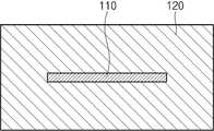
Translated fromKorean도 1은 LR-SPP 모드를 이용한 종래의 금속 광도파로의 구조를 나타낸 단면도.1 is a cross-sectional view showing the structure of a conventional metal optical waveguide using the LR-SPP mode.
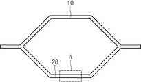
도 2는 도 1의 광도파로를 이용한 종래의 금속 광도파로 센서의 구조를 나타낸 평면도.Figure 2 is a plan view showing the structure of a conventional metal optical waveguide sensor using the optical waveguide of Figure 1;
도 3은 본 발명의 제1실시예에 따른 하이브리드형 광도파로 센서의 구조를 나타낸 사시도.Figure 3 is a perspective view showing the structure of a hybrid optical waveguide sensor according to a first embodiment of the present invention.
도 4는 도 3의 Ⅰ-Ⅰ′선을 따라 자른 단면도.4 is a cross-sectional view taken along the line II ′ of FIG. 3.
도 5의 (a) 및 (b)는 금속 광도파로 및 유전체 광도파로 부분에서의 모드 형태의 시뮬레이션 도면.5 (a) and 5 (b) are simulation diagrams of the mode form in the metal optical waveguide and the dielectric optical waveguide portions.
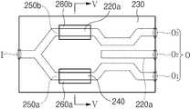
도 6은 본 발명의 제2실시예에 따른 하이브리드형 광도파로 센서의 구조를 나타낸 사시도.Figure 6 is a perspective view showing the structure of a hybrid optical waveguide sensor according to a second embodiment of the present invention.
도 7은 도 6의 Ⅱ-Ⅱ′선을 따라 자른 단면도.FIG. 7 is a cross-sectional view taken along the line II-II ′ of FIG. 6.
도 8은 금속 광도파로 센서와 하이브리드 광도파로 센서에서의 강도(intensity) 모듈레이션의 차이를 계산하여 나타낸 그래프.FIG. 8 is a graph showing calculated differences in intensity modulation in a metal optical waveguide sensor and a hybrid optical waveguide sensor. FIG.
도 9는 제2실시예의 변형예를 나타낸 평면도.9 is a plan view showing a modification of the second embodiment;
도 10은 도 9의 Ⅲ-Ⅲ′선을 따라 자른 단면도.FIG. 10 is a cross-sectional view taken along line III-III ′ of FIG. 9;
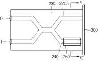
도 11은 본 발명의 제3실시예에 따른 하이브리드형 광도파로 센서의 구조를 나타낸 평면도.11 is a plan view showing the structure of a hybrid optical waveguide sensor according to a third embodiment of the present invention.
도 12는 제3실시예의 변형예를 나타낸 평면도.12 is a plan view showing a modification of the third embodiment.
도 13은 본 발명의 제4실시예에 따른 하이브리드형 광도파로 센서의 구조를 나타낸 평면도.13 is a plan view showing the structure of a hybrid optical waveguide sensor according to a fourth embodiment of the present invention.
도 14는 제4실시예의 변형예를 나타낸 평면도.14 is a plan view showing a modification of the fourth embodiment.
< 도면의 주요 부분에 대한 부호의 설명 ><Description of Symbols for Main Parts of Drawings>
200: 기판210: 금속 박막200: substrate 210: metal thin film
210a: 제1금속 박막210b: 제2금속 박막210a: first metal
220: 유전체층220a: 돌출부220:
230: 폴리머층240: 리셉터층230: polymer layer 240: receptor layer
250a: 제1암(arm)250b: 제2암(arm)250a:
260: 개구부260a: 제1개구부260: opening 260a: first opening
260b: 제2개구부I: 광신호 입력부260b: second opening I: optical signal input
O: 광신호 출력부O1: 제1광신호 출력부O: optical signal output section O1 : first optical signal output section
O2: 제2광신호 출력부O3: 제3광신호 출력부O2 : second optical signal output unit O3 : third optical signal output unit
300: 미러(mirror)면300 mirror surface
본 발명은 하이브리드형 광도파로 센서에 관한 것으로서, 보다 상세하게는, 전파 손실을 줄이고 민감도를 향상시킬 수 있는 하이브리드 광도파로 센서에 관한 것이다.The present invention relates to a hybrid optical waveguide sensor, and more particularly, to a hybrid optical waveguide sensor capable of reducing propagation loss and improving sensitivity.
환경의 변화 및 오염에 따라 환경 센서, 바이오 센서 및 가스 센서 등의 필요성이 점점 증대되고 있다. 특히, 더욱 민감하고 가능한 한 크기가 작아 휴대가 가능한 센서가 필요시되고 있다.As environmental changes and pollution occur, the necessity of environmental sensors, biosensors, and gas sensors is increasing. In particular, there is a need for a sensor that is more sensitive and as small as possible and portable.
지난 수십 년 동안 센서의 개발이 꾸준히 진행되어 왔으며, 센서의 발전에 동원된 여러 기술 중 광학을 이용한 광학 센서에 대한 연구와 기술 개발은 현저한 발전을 거쳐 왔다. 특히, 표면 플라즈몬(SP: Surface Plasmon)을 이용한 센서의 개발은 그 민감도가 다른 기술들의 센서들에 비해 매우 우수하기 때문에 이 표면 플라즈몬(SP) 기술을 응용한 센서의 제작이 많이 이루어지고 있다.In the past decades, the development of sensors has been steadily progressing, and research and technology development of optical sensors using optics have been remarkably developed among several technologies mobilized for the development of sensors. In particular, the development of the sensor using the surface plasmon (SP) (SP) has been made a lot of sensors using the surface plasmon (SP) technology because the sensitivity is very excellent compared to the sensors of other technologies.
상기 표면 플라즈몬(SP)은 유전상수의 실수항이 서로 반대의 부호를 갖는 경계면을 따라 진행하는 전하밀도의 진동파로서 일반적으로 금속(-)과 유전체(+)의 경계에서 존재하며, 전하밀도 진동은 고속으로 가속된 전자 및 광파에 의하여 여기될 수 있다. 표면 플라즈몬(SP)과 결합하여 진행하는 전자기파를 표면 플라즈몬 폴라리톤(Surface Plasmon Polariton, 이하 "SPP"라 한다)이라고 한다.The surface plasmon (SP) is a vibration wave of charge density in which the real term of the dielectric constant propagates along an interface having opposite signs, and is generally present at the boundary between the metal (-) and the dielectric (+). It can be excited by electrons and light waves accelerated at high speed. Electromagnetic waves traveling in conjunction with the surface plasmon SP are called surface plasmon polaritons (hereinafter referred to as "SPP").
표면 플라즈몬(SP)의 파수벡터는 주변물질의 파수벡터 보다 크기 때문에 SPP는 금속표면에 속박된 파동이다. 따라서, 금속과 유전체의 경계면은 경계면과 수직하게 속박조건을 가지는 2차원의 평판 광도파로로 생각할 수 있다.Since the wave vector of the surface plasmon (SP) is larger than the wave vector of the surrounding material, SPP is a wave bound to the metal surface. Therefore, the interface between the metal and the dielectric can be thought of as a two-dimensional flat waveguide having a binding condition perpendicular to the interface.
광도파로의 관점에서 보면, 금속과 유전체의 경계면에서 발생하는 SPP는 표면에 속박되는 효율은 매우 높은 반면, 전파거리가 가시광 영역에서 수십 ㎜로 짧은 단점이 있다. 하지만 금속의 두께를 수 ㎚ 내지 수십 ㎚ 범위로 제한하여 금속의 위아래 경계에서 진행하는 SPP를 상호 결합시키면 광의 장거리 전송이 가능하다. 이를 장거리 표면 플라즈몬 폴라리톤(LR-SPP: Long Range Surface Plasmon Polariton, 이하 LR-SPP라 한다) 모드라고 하는데, LR-SPP의 필드 프로파일(field profile)은 금속선 주변의 유전체에 넓게 분포하여 광의 진행손실이 작으며, 광섬유와의 결합특성도 좋은 장점을 가지고 있어, 다양한 광소자 분야에 응용되고 있다.From the perspective of the optical waveguide, the SPP generated at the interface between the metal and the dielectric has a very high efficiency of being bound to the surface, while having a short propagation distance of several tens of mm in the visible region. However, by limiting the thickness of the metal to a range of several nm to several tens of nm, the SPPs traveling at the upper and lower boundaries of the metal can be mutually coupled to allow long-distance transmission of light. This is called Long Range Surface Plasmon Polariton (LR-SPP) mode. The field profile of the LR-SPP is widely distributed in the dielectric around the metal line, resulting in the loss of light propagation. Its small size and good coupling properties with optical fibers have been applied to various optical device fields.
이하, 도 1 및 도 2를 참조하여 LR-SPP 모드를 이용한 종래의 금속 광도파로 및 이를 이용한 광도파로 센서에 대하여 설명하기로 한다.Hereinafter, a conventional metal optical waveguide using the LR-SPP mode and an optical waveguide sensor using the same will be described with reference to FIGS. 1 and 2.
도 1은 LR-SPP 모드를 이용한 종래의 금속 광도파로의 구조를 나타낸 단면도이다.1 is a cross-sectional view showing the structure of a conventional metal optical waveguide using the LR-SPP mode.
우선, 도 1을 참조하면, 종래의 광도파로는, 단면이 일정한 두께와 폭을 갖고 얇고 긴 스트립(strip) 형태의 금속(110)으로 이루어진 코어, 및 상기 금속(110)으로 이루어진 코어를 둘러싸는 유전체(120)를 포함하며, 이러한 광도파로의 전체 구조 역시 스트립 형태로 이루어질 수 있다.First, referring to FIG. 1, a conventional optical waveguide includes a core having a constant thickness and width and having a core made of a thin and long strip-
이러한 종래의 광도파로는, 단면이 일정한 두께와 폭을 가지며 스트립 형태로 이루어진 금속(110)에 빛을 커플링(coupling)시키고, 상기 금속(110)의 길이 방향으로 SPP 파(wave)가 전파되도록 하고 있다. 이 때, 파(wave)의 진행 방향의 수직인 단면에서 보면 일정한 두께와 폭을 갖기 때문에 2차원에서 구속이 가능하므로 LR-SPP 모드의 광도파로 구현이 가능한 것이다.Such a conventional optical waveguide has a constant thickness and width in cross section and couples light to a
도 2는 도 1의 광도파로를 이용한 종래의 금속 광도파로 센서의 구조를 나타낸 평면도이다.2 is a plan view illustrating a structure of a conventional metal optical waveguide sensor using the optical waveguide of FIG. 1.
도 2에 도시한 바와 같이, 도 1에 도시한 광도파로를 마흐 첸더 간섭계(MZI : Mach-Zehnder Interferometer) 타입으로 구성하여 한쪽 암(arm)(10)은 기준(reference) 신호를, 다른쪽 암(20)은 측정하고자 하는 물질을 광도파로와 상호작용(interaction)시킴으로써 변조된 신호를 받아 발생한 위상차를 검출(detection)함으로써 물질의 종류나 농도 등을 센싱할 수 있다.As shown in FIG. 2, the optical waveguide shown in FIG. 1 is configured as a Mach-Zehnder Interferometer (MZI) type so that one
그러나, 상기와 같이 광도파로의 코어 전체를 금속으로 구성하는 금속 광도파로 센서의 경우, 금속 표면과 감지 물질의 반응을 이용하여 센서로서 사용이 가능한데, 이 때 금속의 반응성 때문에 높은 민감도를 얻을 수는 있지만, 전체적인 전파 손실이 크다는 문제점이 있다.However, in the case of the metal optical waveguide sensor composed of the entire metal core of the optical waveguide as described above, it can be used as a sensor by using the reaction of the metal surface and the sensing material, and high sensitivity can be obtained due to the reactivity of the metal. However, there is a problem that the overall propagation loss is large.
한편, 도면에 도시하지는 않았지만, 일반 유전체의 구조체로 만든 유전체 광도파로 센서는 빛의 진행에 있어서 전파 손실이 거의 없기 때문에 센서로서 기본적인 구조를 유지하는데 상당한 이로움을 가질 수 있다. 그러나, 상기 유전체 광도파로 센서는, 금속 광도파로 센서에 비해 센서로서의 민감도가 떨어지는 문제점이 있었다.On the other hand, although not shown in the drawings, the dielectric optical waveguide sensor made of a structure of a general dielectric can have a considerable advantage in maintaining the basic structure as a sensor because there is little propagation loss in the progress of light. However, the dielectric optical waveguide sensor has a problem inferior in sensitivity as a metal optical waveguide sensor.
따라서, 당 기술분야에서는 전파 손실을 줄이는 동시에 민감도를 향상시킬 수 있는 새로운 방안이 요구되고 있다.Therefore, there is a need in the art for a new method of reducing the propagation loss and improving the sensitivity.
따라서, 본 발명은 상기 문제점을 해결하기 위하여 이루어진 것으로서, 본 발명의 목적은, 전파 손실을 줄이고 민감도를 향상시킬 수 있도록 한 하이브리드형 광도파로 센서를 제공하는데 있다.Accordingly, the present invention has been made to solve the above problems, and an object of the present invention is to provide a hybrid optical waveguide sensor capable of reducing propagation loss and improving sensitivity.
상기 목적을 달성하기 위한 본 발명에 의한 하이브리드형 광도파로 센서는, 일단에 한 개의 광신호 입력부를 가지고, 타단에 한 개의 광신호 출력부를 가지며, 내부의 일부분에 소정 크기의 금속 박막을 구비하는 유전체층; 상기 유전체층의 상하부에 형성되며, 상기 금속 박막과 대응하는 상기 유전체층 부분을 노출시키되, 상기 금속 박막의 폭 보다 큰 폭의 개구부를 갖는 폴리머층; 및 상기 개구부에 의해 노출된 상기 금속 박막과 대응하는 상기 유전체층 부분 상에 형성된 리셉터층;을 포함한다.The hybrid optical waveguide sensor according to the present invention for achieving the above object, has one optical signal input at one end, one optical signal output at the other end, the dielectric layer having a metal thin film of a predetermined size in a portion of the inside ; A polymer layer formed on upper and lower portions of the dielectric layer and exposing a portion of the dielectric layer corresponding to the metal thin film, the polymer layer having an opening having a width larger than that of the metal thin film; And a receptor layer formed on a portion of the dielectric layer corresponding to the metal thin film exposed by the opening.
또한, 상기 유전체층은 그 상면 일부에 돌출부를 가지며, 상기 돌출부는 상기 유전체층 일단의 광신호 입력부와 타단의 광신호 출력부의 사이를 연결하는 직선 형태를 갖는 것을 특징으로 한다.In addition, the dielectric layer may have a protrusion on a portion of an upper surface thereof, and the protrusion may have a straight line connecting an optical signal input part of one end of the dielectric layer and an optical signal output part of the other end.
또한, 상기 돌출부는 상기 금속 박막의 상부를 지나는 것을 특징으로 한다.In addition, the protrusion is characterized in that passing through the upper portion of the metal thin film.
또한, 상기 유전체층은 그 상면 일부에 돌출부를 가지며, 상기 돌출부는 상기 유전체층 일단의 광신호 입력부에서는 한 개의 라인 형태이지만, 도중에 두 개의 라인으로 분기되어 제1암(arm) 및 제2암(arm)을 이루다가 다시 합류되어 상기 광신호 출력부에서는 한 개의 라인 형태로 이루어지는 것을 특징으로 한다.In addition, the dielectric layer has a protrusion on a portion of an upper surface thereof, and the protrusion is in the form of one line in the optical signal input portion of one end of the dielectric layer, but branched into two lines along the first arm and the second arm. After joining again, the optical signal output unit has one line shape.
또한, 상기 돌출부의 제1암은 상기 금속 박막의 상부를 지나는 것을 특징으로 한다.The first arm of the protrusion may pass through an upper portion of the metal thin film.
또한, 상기 금속 박막은, 그 표면을 따라 전송되는 광이 SPP(Surface Plasmon Polariton) 방식으로 전송되는 것을 특징으로 한다.In addition, the metal thin film is characterized in that the light transmitted along its surface is transmitted by the Surface Plasmon Polariton (SPP) method.
그리고, 상기 목적을 달성하기 위한 본 발명에 의한 하이브리드형 광도파로 센서는, 일단에 한 개의 광신호 입력부를 가지고, 타단에 한 개의 광신호 출력부를 가지며, 내부의 일부분에 서로 소정간격 이격 배치된 소정 크기의 제1 및 제2금속 박막을 구비하는 유전체층; 상기 유전체층의 상하부에 형성되며, 상기 제1 및 제2금속 박막과 대응하는 각각의 유전체층 부분을 노출시키되, 상기 제1 및 제2금속 박막의 폭 보다 큰 폭의 제1 및 제2개구부를 갖는 폴리머층; 및 상기 제1개구부에 의해 노출된 상기 제1금속 박막과 대응하는 상기 유전체층 부분 상에 형성된 리셉터층;을 포함한다.In addition, the hybrid optical waveguide sensor according to the present invention for achieving the above object, has one optical signal input unit at one end, one optical signal output unit at the other end, a predetermined interval spaced from each other in a portion of the interior A dielectric layer having first and second metal thin films of size; Polymers formed on upper and lower portions of the dielectric layer and exposing respective portions of the dielectric layer corresponding to the first and second metal thin films and having first and second openings having a width larger than that of the first and second metal thin films. layer; And a receptor layer formed on a portion of the dielectric layer corresponding to the first metal thin film exposed by the first opening.
또한, 상기 유전체층은 그 상면 일부에 돌출부를 가지며, 상기 돌출부는 상기 유전체층 일단의 광신호 입력부에서는 한 개의 라인 형태이지만, 도중에 두 개 의 라인으로 분기되어 제1암(arm) 및 제2암(arm)을 이루다가 다시 합류되어 상기 광신호 출력부에서는 한 개의 라인 형태로 이루어지는 것을 특징으로 한다.In addition, the dielectric layer has a protrusion on a portion of an upper surface thereof, and the protrusion is in the form of one line in the optical signal input portion at one end of the dielectric layer, but branched into two lines along the first arm and the second arm. ) And then joined again to form the line in the optical signal output unit.
또한, 상기 돌출부의 제1암은 상기 제1금속 박막의 상부를 지나고, 상기 제2암은 상기 제2금속 박막의 상부를 지나는 것을 특징으로 한다.The first arm of the protrusion passes through the upper portion of the first metal thin film, and the second arm passes through the upper portion of the second metal thin film.
그리고, 상기 목적을 달성하기 위한 본 발명에 의한 하이브리드형 광도파로 센서는, 일단에 한 개의 광신호 입력부를 가지고, 타단에 세 개의 제1, 제2 및 제3광신호 출력부를 가지며, 내부의 일부분에 소정 크기의 금속 박막을 구비하는 유전체층; 상기 유전체층의 상하부에 형성되며, 상기 금속 박막과 대응하는 상기 유전체층 부분을 노출시키되, 상기 금속 박막의 폭 보다 큰 폭의 개구부를 갖는 폴리머층; 및 상기 개구부에 의해 노출된 상기 금속 박막과 대응하는 상기 유전체층 부분 상에 형성된 리셉터층;을 포함한다.In addition, the hybrid optical waveguide sensor according to the present invention for achieving the above object, has one optical signal input at one end, three first, second and third optical signal output at the other end, a part of the inside A dielectric layer having a metal thin film having a predetermined size; A polymer layer formed on upper and lower portions of the dielectric layer and exposing a portion of the dielectric layer corresponding to the metal thin film, the polymer layer having an opening having a width larger than that of the metal thin film; And a receptor layer formed on a portion of the dielectric layer corresponding to the metal thin film exposed by the opening.
또한, 상기 유전체층은 그 상면 일부에 돌출부를 가지며, 상기 돌출부는 상기 유전체층 일단의 광신호 입력부에서는 한 개의 라인 형태이지만, 도중에 두 개의 라인으로 분기되어 제1암(arm) 및 제2암(arm)을 이루다가, 상기 제1암은 상기 유전체층 타단의 제1광신호 출력부와 연결되고, 상기 제2암은 상기 제3광신호 출력부와 연결되는 것을 특징으로 한다.In addition, the dielectric layer has a protrusion on a portion of an upper surface thereof, and the protrusion is in the form of one line in the optical signal input portion of one end of the dielectric layer, but branched into two lines along the first arm and the second arm. The first arm may be connected to the first optical signal output part at the other end of the dielectric layer, and the second arm may be connected to the third optical signal output part.
또한, 상기 돌출부의 제1암은 상기 금속 박막의 상부를 지나는 것을 특징으로 한다.The first arm of the protrusion may pass through an upper portion of the metal thin film.
또한, 상기 유전체층은 그 상면 일부에 상기 제1 및 제3광신호 출력부 사이 의 제2광신호 출력부에서 일측으로 라인 형태로 연장 형성된 돌출부를 더 갖는 것을 특징으로 한다.The dielectric layer may further include a protrusion formed on a portion of an upper surface of the dielectric layer extending in a line shape to one side from the second optical signal output unit between the first and third optical signal output units.
그리고, 상기 목적을 달성하기 위한 본 발명에 의한 하이브리드형 광도파로 센서는, 일단에 한 개의 광신호 입력부를 가지고, 타단에 세 개의 제1, 제2 및 제3광신호 출력부를 가지며, 내부의 일부분에 서로 소정간격 이격 배치된 소정 크기의 제1 및 제2금속 박막을 구비하는 유전체층; 상기 유전체층의 상하부에 형성되며, 상기 제1 및 제2금속 박막과 대응하는 각각의 유전체층 부분을 노출시키되, 상기 제1 및 제2금속 박막의 폭 보다 큰 폭의 제1 및 제2개구부를 갖는 폴리머층; 및 상기 제1개구부에 의해 노출된 상기 제1금속 박막과 대응하는 상기 유전체층 부분 상에 형성된 리셉터층;을 포함한다.In addition, the hybrid optical waveguide sensor according to the present invention for achieving the above object, has one optical signal input at one end, three first, second and third optical signal output at the other end, a part of the inside A dielectric layer including first and second metal thin films of a predetermined size disposed at a predetermined distance from each other; Polymers formed on upper and lower portions of the dielectric layer and exposing respective portions of the dielectric layer corresponding to the first and second metal thin films and having first and second openings having a width larger than that of the first and second metal thin films. layer; And a receptor layer formed on a portion of the dielectric layer corresponding to the first metal thin film exposed by the first opening.
또한, 상기 유전체층은 그 상면 일부에 돌출부를 가지며, 상기 돌출부는 상기 유전체층 일단의 광신호 입력부에서는 한 개의 라인 형태이지만, 도중에 두 개의 라인으로 분기되어 제1암(arm) 및 제2암(arm)을 이루다가, 상기 제1암은 상기 유전체층 타단의 제1광신호 출력부와 연결되고, 상기 제2암은 상기 제3광신호 출력부와 연결되는 것을 특징으로 한다.In addition, the dielectric layer has a protrusion on a portion of an upper surface thereof, and the protrusion is in the form of one line in the optical signal input portion of one end of the dielectric layer, but branched into two lines along the first arm and the second arm. The first arm may be connected to the first optical signal output part at the other end of the dielectric layer, and the second arm may be connected to the third optical signal output part.
또한, 상기 돌출부의 제1암은 상기 제1금속 박막의 상부를 지나고, 상기 제2암은 상기 제2금속 박막의 상부를 지나는 것을 특징으로 한다.The first arm of the protrusion passes through the upper portion of the first metal thin film, and the second arm passes through the upper portion of the second metal thin film.
또한, 상기 유전체층은 그 상면 일부에 상기 제1 및 제3광신호 출력부 사이의 제2광신호 출력부에서 일측으로 라인 형태로 연장 형성된 돌출부를 더 갖는 것 을 특징으로 한다.In addition, the dielectric layer may further include a protrusion extending in a line shape to one side from the second optical signal output unit between the first and third optical signal output units.
그리고, 상기 목적을 달성하기 위한 본 발명에 의한 하이브리드형 광도파로 센서는, 일단에 한 개의 광신호 입력부 및 한 개의 광신호 출력부를 모두 가지며, 내부의 일부분에 소정 크기의 금속 박막을 구비하는 유전체층; 상기 유전체층의 상하부에 형성되며, 상기 금속 박막과 대응하는 상기 유전체층 부분을 노출시키되, 상기 금속 박막의 폭 보다 큰 폭의 개구부를 갖는 폴리머층; 및 상기 개구부에 의해 노출된 상기 금속 박막과 대응하는 상기 유전체층 부분 상에 형성된 리셉터층;을 포함한다.In addition, the hybrid optical waveguide sensor according to the present invention for achieving the above object, has one optical signal input portion and one optical signal output portion at one end, a dielectric layer having a metal thin film of a predetermined size in a portion thereof; A polymer layer formed on upper and lower portions of the dielectric layer and exposing a portion of the dielectric layer corresponding to the metal thin film, the polymer layer having an opening having a width larger than that of the metal thin film; And a receptor layer formed on a portion of the dielectric layer corresponding to the metal thin film exposed by the opening.
또한, 상기 유전체층은 그 상면 일부에 돌출부를 가지며, 상기 돌출부는 상기 유전체층 일단의 광신호 입력부 및 광신호 출력부에서는 각각 독립된 라인 형태이지만, 도중에 합류되어 한 개의 라인을 이루다가 다시 분기되어 상기 유전체층의 타단까지 각각 연장되는 것을 특징으로 한다.In addition, the dielectric layer has a protrusion on a portion of an upper surface thereof, and the protrusion is a separate line in the optical signal input unit and the optical signal output unit at one end of the dielectric layer, but joins in the middle to form a line, and then branches again to form the dielectric layer. It is characterized by extending to the other end, respectively.
또한, 상기 돌출부는 상기 금속 박막의 상부를 지나는 것을 특징으로 한다.In addition, the protrusion is characterized in that passing through the upper portion of the metal thin film.
또한, 상기 유전체층의 타단에는 미러(mirror)면이 구비되어 있는 것을 특징으로 한다.In addition, the other end of the dielectric layer is characterized in that the mirror surface (mirror) is provided.
또한, 상기 유전체층은 그 상면 일부에 돌출부를 가지며, 상기 돌출부는 상기 유전체층 일단의 광신호 입력부 및 광신호 출력부에서 각각 독립된 라인 형태이며, 상기 독립된 라인은 상기 유전체층의 타단까지 각각 연장되는 것을 특징으로 한다.In addition, the dielectric layer has a protrusion on a portion of an upper surface thereof, and the protrusion is in the form of a line separate from each of the optical signal input and the optical signal output of one end of the dielectric layer, wherein the independent line extends to the other end of the dielectric layer, respectively. do.
본 발명의 하이브리드형 광도파로 센서의 상기 목적에 대한 기술적 구성을 비롯한 작용효과에 관한 사항은 본 발명의 바람직한 실시예가 도시된 도면을 참조한 아래의 상세한 설명에 의해서 명확하게 이해될 것이다.Matters relating to the operational effects including the technical configuration for the above object of the hybrid optical waveguide sensor of the present invention will be clearly understood by the following detailed description with reference to the drawings showing preferred embodiments of the present invention.
제1실시예First embodiment
도 3 내지 도 5를 참조하여 본 발명의 제1실시예에 따른 하이브리드형 광도파로 센서에 대하여 상세히 설명한다.The hybrid optical waveguide sensor according to the first embodiment of the present invention will be described in detail with reference to FIGS. 3 to 5.
우선, 도 3은 본 발명의 제1실시예에 따른 하이브리드형 광도파로 센서의 구조를 나타낸 사시도이고, 도 4는 도 3의 Ⅰ-Ⅰ′선을 따라 자른 단면도이다.First, FIG. 3 is a perspective view illustrating a structure of a hybrid optical waveguide sensor according to a first embodiment of the present invention, and FIG. 4 is a cross-sectional view taken along the line II ′ of FIG. 3.
도 3 및 도 4에 도시한 바와 같이, 본 발명의 제1실시예에 따른 하이브리드형 광도파로 센서는, 일단에 한 개의 광신호 입력부(I)를 가지고, 타단에 한 개의 광신호 출력부(O)를 가지며, 내부의 일부분에 소정 크기의 금속 박막(210)을 구비하는 유전체층(220)을 구비하고 있다.3 and 4, the hybrid optical waveguide sensor according to the first embodiment of the present invention has one optical signal input unit I at one end and one optical signal output unit O at the other end. And a
상기 유전체층(220)의 상하부에는, 상기 금속 박막(210)과 대응하는 상기 유전체층(220) 부분을 노출시키되, 상기 금속 박막(210)의 폭 보다 큰 폭의 개구부(260)를 갖는 폴리머층(230)이 형성되어 있다. 여기서, 상기 금속 박막(210) 및 유전체층(220)을 포함한 상기 폴리머층(230)은 기판(200) 상에 형성되어 있다.Upper and lower portions of the
상기 개구부(260)에 의해 노출된, 상기 금속 박막(210)과 대응하는 상기 유전체층(220) 부분 상에는 리셉터(receptor)층(240)이 형성되어 있다.A
그리고, 상기 유전체층(220)의 상면 일부에는 돌출부(220a)가 구비되어 있는데, 상기 돌출부(220a)는 상기 유전체층(220) 일단의 상기 광신호 입력부(I)와 타단의 광신호 출력부(O)의 사이를 연결하는 직선 형태를 갖고 있다. 이 때, 상기 돌출부(220a)는 상기 금속 박막(210)의 상부를 지나는 것이 바람직하다.A portion of the upper surface of the
상기 금속 박막(210)과, 그 상부 및 하부에 형성된 유전체층(220)으로 이루어진 금속 광도파로 부분은 반응 파트를 구성하게 되고, 상기 반응 파트를 제외한 부분, 즉 상기 금속 박막(210)이 형성되지 않은 부분의 돌출부(220a) 부분과, 그 하부의 유전체층(220) 부분은 유전체 광도파로 파트를 구성하게 된다.The metal optical waveguide part including the metal
즉, 본 발명은 기존의 유전체 광도파로가 갖는 낮은 민감도를 극복하기 위해서, 상술한 바와 같이 금속 박막(210)을 이용한 금속 광도파로를 센서 파트로 사용하되, 전체의 구조를 상기 금속 광도파로로 구성할 경우 높은 전파 손실로 인해, 센서를 구성함에 있어서 전파 길이(propagation length) 등에 제한을 받을 수 있으므로, 반응 파트는 상기와 같이 금속 박막(210) 및 이를 감싸는 유전체층(220)으로 이루어진 금속 광도파로로 구성하고, 그 외의 광도파로는 유전체층(220)으로 이루어진 유전체 광도파로로 구성하는 형태의 하이브리드형 광도파로 센서를 구현하고 있다.That is, in order to overcome the low sensitivity of the existing dielectric optical waveguide, the present invention uses a metal optical waveguide using the metal
여기서, 반응 파트의 상기 금속 박막(210)은, 그 표면을 따라 전송되는 광이 SPP(Surface Plasmon Polariton) 방식으로 전송되는 것이 바람직하다. 즉, 본 발명에 의한 하이브리드형 광도파로 센서의 신호 전송방법은 상기 SPP 방식을 이용하는 것이다.Here, the metal
이러한 본 발명의 하이브리드형 광도파로 센서는, 반응 파트를 제외한 부분은 전파 손실이 적은 유전체층(220)으로 입출력빔을 안내(guiding)하고, 상기 반응 파트는 금속 박막(210)을 포함하는 금속 광도파로로 구성함으로써, 상기 금속 광도파로의 상기 SPP 특성에 의해 뛰어난 민감도(sensitivity)를 가질 수 있다.In the hybrid optical waveguide sensor of the present invention, the portion except for the reaction part guides the input / output beam to the
도 5의 (a) 및 (b)는 금속 광도파로 및 유전체 광도파로 부분에서의 모드 형태의 시뮬레이션 도면이다.5 (a) and 5 (b) are simulation diagrams of the mode form in the metal optical waveguide and the dielectric optical waveguide portions.
본 발명에서는, 도 5에 나타난 바와 같이 각각의 모드 형태를 유사하게 만들어 줌으로써, 센서 양 끝단에서의 접속 손실(coupling loss)를 줄일 수 있다.In the present invention, as shown in FIG. 5, by making the respective mode shapes similar, coupling loss at both ends of the sensor can be reduced.
이 때, 상기 금속 박막(210)의 폭과 두께, 그리고 유전체 광도파로의 형태에 따라서 모드의 크기 및 형태에 변화를 줄 수 있다.In this case, the size and shape of the mode may be changed according to the width and thickness of the metal
이러한 본 발명의 하이브리드형 광도파로 센서는, 상기 개구부(260)에 의해 노출된, 금속 박막(210) 상부의 유전체층(220) 상에 형성된 리셉터층(240)을 측정하고자 하는 물질에 노출시키고, 측정하고자 하는 물질이 상기 리셉터층(240)과 반응할 때의 변화를 상기 금속 박막(210)에 발생하는 SPP 모드와의 상호작용(interaction)에 의해 입력(input)과 출력(output) 간의 전파손실을 측정하여 확인할 수 있다.The hybrid optical waveguide sensor of the present invention exposes the
즉, 본 발명은 측정하고자 하는 물질이 반응 파트에 형성된 리셉터층(240)과 반응할 때, 상기 리셉터층(240) 주위의 외부 굴절률이 변하게 되고, 상기 금속 박막(210)을 포함한 금속 광도파로 상의 물질의 두께가 변화된다. 이 때, 금속 박막(210)에서 SPP 모드가 물질 변화와 상호작용을 하게 되고, 이는 빛의 강도(intensity)의 변화에 영향을 줌으로써, 이를 측정하여 굴절률 및 두께의 변화를 측정할 수 있다.That is, in the present invention, when the material to be measured reacts with the
이러한 하이브리드 광도파로 센서를 구성함에 따라 입사될 때의 강도를 최대한으로 보존할 수 있고, 금속 박막(210)에서의 물질 반응에 따른 강도의 큰 차이를 얻을 수 있으며, 유전체 광도파로 파트에서는 전파 손실을 최소화하여 변화된 강도의 신호를 최대로 얻을 수 있다.By constructing such a hybrid optical waveguide sensor, it is possible to preserve the intensity at the time of incidence to the maximum, and to obtain a large difference in intensity according to the material reaction in the metal
또한, 본 발명은 필요한 기능에 따라 물질들의 두께 및 유전상수를 조절할 수 있으므로, 필요한 기능을 갖는 광도파로로 최적화시킬 수 있고, 간단한 구조로 센서 어레이 구성이 용이하다.In addition, the present invention can adjust the thickness and dielectric constant of the material according to the required function, it can be optimized to the optical waveguide having the required function, it is easy to configure the sensor array with a simple structure.
제2실시예Second embodiment
도 6 및 도 7을 참조하여 본 발명의 제2실시예에 따른 하이브리드형 광도파로 센서에 대하여 상세히 설명한다. 다만, 제2실시예의 구성 중 제1실시예와 동일한 부분에 대한 설명은 생략하고, 제 2 실시예에서 달라지는 구성에 대해서만 상술하기로 한다.A hybrid optical waveguide sensor according to a second exemplary embodiment of the present invention will be described in detail with reference to FIGS. 6 and 7. However, the description of the same parts as the first embodiment of the configuration of the second embodiment will be omitted, and only the configuration that is different from the second embodiment will be described in detail.
도 6은 본 발명의 제2실시예에 따른 하이브리드형 광도파로 센서의 구조를 나타낸 사시도이고, 도 7은 도 6의 Ⅱ-Ⅱ′선을 따라 자른 단면도이다.6 is a perspective view illustrating a structure of a hybrid optical waveguide sensor according to a second exemplary embodiment of the present invention, and FIG. 7 is a cross-sectional view taken along the line II-II ′ of FIG. 6.
본 발명의 제2실시예에 따른 하이브리드형 광도파로 센서는, 제1실시예에 따른 하이브리드형 광도파로 센서와 대부분의 구성이 동일하고, 다만, 도 6 및 도 7 에 도시한 바와 같이, 상기 돌출부(220a)는 상기 유전체층(220) 일단의 광신호 입력부(I)에서는 한 개의 라인 형태이지만, 도중에 두 개의 라인으로 분기되어 제1암(arm)(250a) 및 제2암(250b)을 이루다가 다시 합류되어 상기 광신호 출력부(O)에서는 한 개의 라인 형태로 이루어진다는 점에서만 제1실시예와 다르다.The hybrid optical waveguide sensor according to the second embodiment of the present invention has the same configuration as that of the hybrid optical waveguide sensor according to the first embodiment, except that the protrusions are illustrated in FIGS. 6 and 7. 220a is in the form of one line in the optical signal input unit I of one end of the
이 때, 상기 돌출부(220a)의 제1암(250a)은 상기 금속 박막(210)의 상부를 지나는 것이 바람직하다.At this time, it is preferable that the
즉, 본 발명의 제2실시예에서는 광도파로를 마흐 첸더 간섭계(MZI : Mach-Zehnder Interferometer) 타입으로 구성하여, 상기 금속 박막(210)의 상부를 지나지 않는 상기 제2암(250b)은 기준이 되는 기준(reference) 신호를, 그리고 상기 금속 박막(210)의 상부를 지나는 제1암(250a)은 측정하고자 하는 물질을 리셉터층(240)과 상호작용시킴으로써 변조된 신호를 받아 양단의 간섭신호에 의해 발생한 위상차를 검출함으로써 물질의 굴절률 변화와 두께 변화 등을 측정할 수 있는 것이다.That is, in the second embodiment of the present invention, the optical waveguide is configured as a Mach-Zehnder Interferometer (MZI) type, so that the
이러한 본 발명에 의한 MZI 타입의 하이브리드형 광도파로 센서는, 기존의 금속 박막만을 이용한 금속 광도파로 센서에 비해서 전체적인 전파 손실의 측면에서 훨씬 더 향상된 특성을 얻을 수 있다.The hybrid optical waveguide sensor of the MZI type according to the present invention can obtain much more improved characteristics in terms of overall propagation loss than the metal optical waveguide sensor using only a metal thin film.
이를 계산하기 위해 본 발명에서는, 유전체 광도파로 파트를 유전체층(220)의 일부 상면에 돌출부(220a)가 형성된 리브/리지(rib/ridge) 형태의 광도파로로 구성하였다.In order to calculate this, in the present invention, the dielectric optical waveguide part is configured as a rib / ridge type optical waveguide in which
전체 6㎜ 길이의 MZI 타입 광도파로 센서를 구성함에 있어서, 종래기술에서와 같이 전체적으로 금속 박막을 이용하여 LR-SPP 센서를 구성할 경우, 전체 전파 손실이 10 dB 이상의 값을 갖는 반면, 본 발명에서와 같이 반응 파트만을 금속 박막으로 구성한 경우, 약 0.56 dB의 전파 손실이 발생하였으며, 상기한 리브/리지 형태의 유전체 광도파로 파트와의 접속 손실(coupling loss)은 약 0.27 dB 정도 발생한다. 이러한 경우의 전체 전파 손실은 1 dB 내지 2 dB 정도밖에 되지 않으므로, 본 발명은 센서의 길이에 크게 제약을 받지 않고 민감도가 우수한 센서를 구현할 수 있게 된다.In constructing the MZI type optical waveguide sensor having a total length of 6 mm, when the LR-SPP sensor is constructed using a metal thin film as a whole, as in the prior art, the total propagation loss has a value of 10 dB or more, As described above, when only the reaction part is formed of a metal thin film, a propagation loss of about 0.56 dB occurs, and a coupling loss with the rib / ridge type dielectric optical waveguide part occurs about 0.27 dB. In this case, since the total propagation loss is only about 1 dB to 2 dB, the present invention can realize a sensor having excellent sensitivity without being significantly limited by the length of the sensor.
도 8은 금속 광도파로 센서와 하이브리드 광도파로 센서에서의 강도(intensity) 모듈레이션의 차이를 계산하여 나타낸 그래프이다.FIG. 8 is a graph showing calculated differences in intensity modulation in a metal optical waveguide sensor and a hybrid optical waveguide sensor.
도 8을 참조하면, 본 계산에서와 같이, 금속 광도파로 센서(Metal waveguide sensor)에서의 전파 손실로 인해 그에 대한 강도의 차이가 발생되는 바, 상기 금속 광도파로 센서에서보다 하이브리드 광도파로 센서에서 고감도의 측정 분해능(resolution)을 얻을 수 있다. 또한, 유전체 광도파로 센서와 비교할 때, 상기 유전체 광도파로 센서는 2×10⁻⁶ 내지 2×10⁻⁷의 굴절률 변화를 측정할 수 있는 반면, 하이브리드 광도파로 센서는 7×10⁻⁸ 내지 7×10⁻⁹의 굴절률 변화 측정이 가능하다.Referring to FIG. 8, as in the present calculation, a difference in intensity occurs due to a propagation loss in a metal waveguide sensor, and thus a high sensitivity is detected in a hybrid waveguide sensor than in the metal waveguide sensor. The measurement resolution of can be obtained. In addition, when compared with dielectric optical waveguide sensors, the dielectric optical waveguide sensor can measure a change in refractive index of 2 × 10⁻⁶ to 2 × 10⁻⁷ , while a hybrid optical waveguide sensor is 7 × 10⁻⁸ to 7 ×. A refractive index change of 10−9 can be measured.
이러한 본 발명의 제2실시예에 따른 하이브리드형 광도파로 센서는, 앞서 상술한 제1실시예에서와 동일한 작용 및 효과를 얻을 수 있다.The hybrid optical waveguide sensor according to the second embodiment of the present invention can obtain the same effects and effects as in the above-described first embodiment.
제2실시예의 변형예Modification of the second embodiment
도 9 및 도 10을 참조하여 제2실시예의 변형예에 대해 설명하기로 한다.A modification of the second embodiment will be described with reference to FIGS. 9 and 10.
도 9는 제2실시예의 변형예를 나타낸 평면도이고, 도 10은 도 9의 Ⅲ-Ⅲ′선을 따라 자른 단면도이다.9 is a plan view illustrating a modification of the second embodiment, and FIG. 10 is a cross-sectional view taken along line III-III ′ of FIG. 9.
제2실시예의 변형예에 따른 하이브리드형 광도파로 센서는, 상술한 바와 같은 제2실시예에 따른 하이브리드형 광도파로 센서와 대부분의 구성이 동일하고, 다만, 도 9 및 도 10에 도시한 바와 같이, 상기 제2암(250b) 하부의 유전체층(220) 내에 제2금속 박막(210b)이 더 구비되어 있다는 점에서 제2실시예와 다르다.The hybrid optical waveguide sensor according to the modification of the second embodiment has the same configuration as most of the hybrid optical waveguide sensor according to the second embodiment as described above, except that as shown in FIGS. 9 and 10. The second metal
즉, 본 발명의 제2실시예의 변형예에 따른 하이브리드형 광도파로 센서는, 일단에 한 개의 광신호 입력부(I)를 가지고, 타단에 한 개의 광신호 출력부(O)를 가지며, 내부의 일부분에 서로 소정간격 이격 배치된 소정 크기의 제1금속 박막(210b) 및 제2금속 박막(210b)을 구비하는 유전체층(220)과, 상기 유전체층(220)의 상하부에 형성되며, 상기 제1 및 제2금속 박막(210a,210b)과 대응하는 각각의 유전체층(220) 부분을 노출시키되, 상기 제1 및 제2금속 박막(210a,210b)의 폭 보다 큰 폭의 제1 및 제2개구부(260a,260b)를 갖는 폴리머층(230)을 포함한다.That is, the hybrid optical waveguide sensor according to the modification of the second embodiment of the present invention has one optical signal input unit I at one end, and one optical signal output unit O at the other end, and a part of the inside. A
상기 유전체층(220)은 그 상면 일부에 돌출부(220a)를 가지며, 상기 돌출부(220a)는 상기 유전체층(220) 일단의 광신호 입력부(I)에서는 한 개의 라인 형태이지만, 도중에 두 개의 라인으로 분기되어 제1암(250a) 및 제2암(250b)을 이루다가 다시 합류되어 상기 광신호 출력부(O)에서는 한 개의 라인 형태로 이루어진다.The
여기서, 상기 돌출부(220a)의 제1암(250a)은 상기 제1금속 박막(210a)의 상부를 지나고, 상기 제2암(250b)은 상기 제2금속 박막(210b)의 상부를 지나는 것이 바람직하다.Here, the
특히, 제2실시예의 변형예에서는, 상기 제1개구부(260a)에 의해 노출된, 상기 제1금속 박막(210a)과 대응하는 상기 유전체층(220) 부분 상에만 리셉터층(240)이 형성되어 있고, 상기 제2개구부(260b)에 의해 노출된 유전체층(220) 부분에는 리셉터층이 형성되어 있지 않다.In particular, in the modification of the second embodiment, the
이는, 기준 파트인 제2암(250b)의 일부와 반응 파트인 제1암(250a)의 일부를 동일한 조건으로 만들어 주어, 반응에 대한 실제적인 민감도를 더욱 향상시키도록 구성한 것이다. 즉, 제2실시예의 경우 리셉터층(240)이 형성된 반응 파트에만 측정하고자 하는 반응 물질을 투입하는 형태이지만, 변형예에서는 기준 파트와 반응 파트에 측정하고자 하는 물질을 함께 투입함으로써, 특이 반응 물질에 대한 신호에 대해서 상기한 파트간의 차이를 줄여줌으로써, 실제적인 조건을 맞추어 주는 것이다.This is configured to make a part of the
이러한 제2실시예의 변형예에는, 제2실시예에서와 동일한 작용 및 효과를 얻을 수 있을 뿐만 아니라, 상기한 바와 같이 상기 제2암(250b) 부분에 리셉터층을 제외한 금속 박막(210)을 포함한 반응 파트를 추가로 구성함으로써, 측정하고자 하는 물질이 존재하는 주변 환경 상태를 함께 측정하여 더욱 정확한 센싱을 할 수 있는 장점이 있다.In the modified example of the second embodiment, the same operation and effect as in the second embodiment can be obtained, and as described above, the
제3실시예Third embodiment
도 11 및 앞서의 도 7을 참조하여 본 발명의 제3실시예에 따른 하이브리드형 광도파로 센서에 대하여 상세히 설명한다.A hybrid optical waveguide sensor according to a third embodiment of the present invention will be described in detail with reference to FIGS. 11 and 7.
도 11은 본 발명의 제3실시예에 따른 하이브리드형 광도파로 센서의 구조를 나타낸 평면도이다. 또한, 도 7은 도 11의 Ⅳ-Ⅳ′선을 따라 자른 단면도이기도 하다.11 is a plan view showing the structure of a hybrid optical waveguide sensor according to a third embodiment of the present invention. 7 is a cross-sectional view taken along the line IV-IV 'of FIG. 11.
본 발명의 제3실시예에 따른 하이브리드형 광도파로 센서는, 도 11 및 앞서의 도 4에 도시한 바와 같이, 일단에 한 개의 광신호 입력부(I)를 가지고, 타단에 세 개의 제1, 제2 및 제3광신호 출력부(O1,O2,O3)를 가지며, 내부의 일부분에 소정 크기의 금속 박막(210)을 구비하는 유전체층(220)과, 상기 유전체층(220)의 상하부에 형성되며, 상기 금속 박막(210)과 대응하는 상기 유전체층(220) 부분을 노출시키되, 상기 금속 박막(210)의 폭 보다 큰 폭의 개구부(260)를 갖는 폴리머층(230), 및 상기 개구부(260)에 의해 노출된 상기 금속 박막(210)과 대응하는 상기 유전체층(220) 부분 상에 형성된 리셉터층(240)을 포함한다.The hybrid optical waveguide sensor according to the third exemplary embodiment of the present invention has one optical signal input unit I at one end and three first and third ends at the other end, as shown in FIGS. 11 and 4. A
상기 유전체층(220)은 그 상면 일부에 돌출부(220a)를 가지며, 상기 돌출부(220a)는 상기 유전체층(220) 일단의 광신호 입력부(I)에서는 한 개의 라인 형태이지만, 도중에 두 개의 라인으로 분기되어 제1암(250a) 및 제2암(250b)을 이루다가, 상기 제1암(250a)은 상기 유전체층(220) 타단의 제1광신호 출력부(O1)와 연결되고, 상기 제2암(250b)은 상기 제3광신호 출력부(O3)와 연결되어 있다.The
여기서, 상기 돌출부(220a)의 제1암(250a)은 상기 금속 박막(210)의 상부를 지나는 것이 바람직하다.Here, the
그리고, 상기 유전체층(220)은, 그 상면 일부에 상기 제1 및 제3광신호 출력부(O1,O3) 사이의 제2광신호 출력부(O2)에서 일측으로 라인 형태로 연장 형성된 돌출부(220a)를 더 갖고 있다.The
이러한 본 발명의 제3실시예에 의한 하이브리드형 광도파로 센서는, 앞서의 다른 실시예들과 마찬가지로 유전체 광도파로와 금속 광도파로를 같이 혼합하여 커플러(coupler) 타입의 간섭계에 적용하고, 출력부를 세 개의 커플러로 구성한 것이다.In the hybrid optical waveguide sensor according to the third embodiment of the present invention, the dielectric optical waveguide and the metal optical waveguide are mixed together and applied to a coupler type interferometer, and the output unit It consists of two couplers.
상술한 바와 같은 제2실시예에 따른 MZI 타입에서는 두 개의 빛을 재합성하여 신호를 구성하는 반면, 본 실시예의 경우는 세 개의 커플러를 이용하여 두 개의 광도파로로 모드 커플링이 파워를 교환하는데 이용되는 것이다. 세 개의 라인에서 각각 2π/3의 위상 변이(phase shift)를 갖게 되고, 이 기술을 사용하여 최적의 출력값을 선택하여 작은 위상 변이를 측정할 수 있고, 유효 인덱스(effective index) 변화 측정을 세 개의 출력부(O1,O2,O3)를 비교하여 측정하는 것이 가능하다.In the MZI type according to the second embodiment as described above, a signal is formed by resynthesizing two lights, whereas in the present embodiment, mode coupling exchanges power with two optical waveguides using three couplers. It is used. Each of the three lines will have a phase shift of 2π / 3, and this technique can be used to select the optimum output value to measure small phase shifts, and to measure the effective index change. It is possible to compare and measure the outputs (O1 , O2 , O3 ).
즉, 제3실시예에서는 세 개의 신호를 비교하여 같은 강도 변화에 대해서도 어느 정도의 유효 인덱스 변화를 나타내는지 각각의 위상 변이를 통해서 구별하는 것이 가능한 장점이 있다.That is, in the third embodiment, there is an advantage that it is possible to distinguish three signals by comparing the three signals to show how much the effective index change even for the same intensity change.
제3실시예의 변형예Modification of the third embodiment
도 12 및 앞서의 도 10을 참조하여 제3실시예의 변형예에 대해 설명하기로 한다.A modification of the third embodiment will be described with reference to FIG. 12 and FIG. 10 above.
도 12는 제3실시예의 변형예를 나타낸 평면도이다. 또한, 도 10은 도 12의 Ⅴ-Ⅴ′선을 따라 자른 단면도이기도 하다.12 is a plan view showing a modification of the third embodiment. 10 is a cross-sectional view taken along the line VV ′ of FIG. 12.
제3실시예의 변형예에 따른 하이브리드형 광도파로 센서는, 상술한 바와 같은 제3실시예에 따른 하이브리드형 광도파로 센서와 대부분의 구성이 동일하고, 다만, 도 12 및 도 10에 도시한 바와 같이, 상기 제2암(250b) 하부의 유전체층(220) 내에 제2금속 박막(210b)이 더 구비되어 있다는 점에서 제2실시예와 다르다.The hybrid optical waveguide sensor according to the modification of the third embodiment has the same configuration as that of the hybrid optical waveguide sensor according to the third embodiment as described above. However, as shown in FIGS. 12 and 10. The second metal
자세하게, 제3실시예의 변형예에 따른 하이브리드형 광도파로 센서는, 일단에 한 개의 광신호 입력부(I)를 가지고, 타단에 세 개의 제1, 제2 및 제3광신호 출력부(O1,O2,O3)를 가지며, 내부의 일부분에 서로 소정간격 이격 배치된 소정 크기의 제1 및 제2금속 박막(210a,210b)을 구비하는 유전체층(220)과, 상기 유전체층(220)의 상하부에 형성되며, 상기 제1 및 제2금속 박막(210a,210b)과 대응하는 각각의 유전체층(220) 부분을 노출시키되, 상기 제1 및 제2금속 박막(210a,210b)의 폭 보다 큰 폭의 제1 및 제2개구부(260a,260b)를 갖는 폴리머층(230), 및 상기 제1개구부(260a)에 의해 노출된 상기 제1금속 박막(210a)과 대응하는 상기 유전체층(220) 부분 상에 형성된 리셉터층(240)을 포함한다.In detail, the hybrid optical waveguide sensor according to the modification of the third embodiment has one optical signal input unit I at one end and three first, second and third optical signal output units O1 , at the other end. O2, O3), the having, upper and lower portions of the
여기서, 상기 유전체층(220)은 그 상면 일부에 돌출부(220a)를 가지며, 상기 돌출부(220a)는 상기 유전체층(220) 일단의 광신호 입력부(I)에서는 한 개의 라인 형태이지만, 도중에 두 개의 라인으로 분기되어 제1암(250a) 및 제2암(250b)을 이 루다가, 상기 제1암(250a)은 상기 유전체층(220) 타단의 제1광신호 출력부(O1)와 연결되고, 상기 제2암(250b)은 상기 제3광신호 출력부(O3)와 연결되어 있다.Here, the
이 때, 상기 돌출부(220a)의 제1암(250a)은 상기 제1금속 박막(210a)의 상부를 지나고, 상기 제2암(250b)은 상기 제2금속 박막(210b)의 상부를 지나는 것이 바람직하다.At this time, the
또한, 상기 유전체층(220)은, 그 상면 일부에 상기 제1 및 제3광신호 출력부(O1,O3) 사이의 제2광신호 출력부(O2)에서 일측으로 라인 형태로 연장 형성된 돌출부(220a)를 더 갖고 있다.In addition, the
이와 같은 제3실시예의 변형예에서는, 상기 제1개구부(260a)에 의해 노출된 유전체층(220) 부분 상에만 리셉터층(240)이 형성되어 있고, 상기 제2개구부(260b)에 의해 노출된 유전체층(220) 부분에는 리셉터층이 형성되어 있지 않다.In this modification of the third embodiment, the
이는, 기준 파트인 제2암(250b)의 일부와 반응 파트인 제1암(250a)의 일부를 동일한 조건으로 만들어 주어, 반응에 대한 실제적인 민감도를 더욱 향상시키도록 구성한 것이다. 즉, 제3실시예의 경우 리셉터층(240)이 형성된 반응 파트에만 측정하고자 하는 반응 물질을 투입하는 형태이지만, 변형예에서는 기준 파트와 반응 파트에 측정하고자 하는 물질을 함께 투입함으로써, 특이 반응 물질에 대한 신호에 대해서 상기한 파트간의 차이를 줄여줌으로써, 실제적인 조건을 맞추어 주는 것이다.This is configured to make a part of the
이러한 제3실시예의 변형예에는, 제3실시예에서와 동일한 작용 및 효과를 얻을 수 있을 뿐만 아니라, 상기한 바와 같이 상기 제2암(250b) 부분에 리셉터층을 제외한 금속 박막(210)을 포함한 반응 파트를 추가로 구성함으로써, 측정하고자 하는 물질이 존재하는 주변 환경 상태를 함께 측정하여 더욱 정확한 센싱을 할 수 있는 장점이 있다.In the modified example of the third embodiment, the same operation and effect as in the third embodiment can be obtained, and as described above, the
제4실시예Fourth embodiment
도 13 및 앞서의 도 7을 참조하여 본 발명의 제4실시예에 따른 하이브리드형 광도파로 센서에 대하여 상세히 설명한다.A hybrid optical waveguide sensor according to a fourth embodiment of the present invention will be described in detail with reference to FIG. 13 and FIG. 7.
도 13은 본 발명의 제4실시예에 따른 하이브리드형 광도파로 센서의 구조를 나타낸 평면도이다. 또한, 도 7은 도 13의 Ⅵ-Ⅵ′선을 따라 자른 단면도이기도 하다.13 is a plan view showing the structure of a hybrid optical waveguide sensor according to a fourth embodiment of the present invention. 7 is a cross-sectional view taken along the line VI-VI ′ of FIG. 13.
본 발명의 제4실시예에 따른 하이브리드형 광도파로 센서는, 도 13 및 앞서의 도 7에 도시한 바와 같이, 일단에 한 개의 광신호 입력부(I) 및 한 개의 광신호 출력부(O)를 모두 가지며, 내부의 일부분에 소정 크기의 금속 박막(210)을 구비하는 유전체층(220)과, 상기 유전체층(220)의 상하부에 형성되며, 상기 금속 박막(210)과 대응하는 상기 유전체층(220) 부분을 노출시키되, 상기 금속 박막(210)의 폭 보다 큰 폭의 개구부(260)를 갖는 폴리머층(230), 및 상기 개구부(260)에 의해 노출된 상기 금속 박막(210)과 대응하는 상기 유전체층(220) 부분 상에 형성된 리셉터층(240)을 포함한다.In the hybrid optical waveguide sensor according to the fourth embodiment of the present invention, one optical signal input unit I and one optical signal output unit O are provided at one end as shown in FIGS. 13 and 7. A
상기 유전체층(220)은 그 상면 일부에 돌출부(220a)를 가지며, 상기 돌출 부(220a)는 상기 유전체층(220) 일단의 광신호 입력부(I) 및 광신호 출력부(O)에서는 각각 독립된 라인 형태이지만, 도중에 합류되어 한 개의 라인을 이루다가 다시 분기되어 상기 유전체층(220)의 타단까지 각각 연장되어 있다.The
이 때, 상기 돌출부(220a)는 상기 금속 박막(210)의 상부를 지나는 것이 바람직하다.At this time, the
특히, 본 발명의 제4실시예에 의한 하이브리드 광도파로 센서는, 상기 유전체층(220)의 타단에는 미러(mirror)면(300)을 구비하고 있다.In particular, the hybrid optical waveguide sensor according to the fourth embodiment of the present invention includes a
이와 같이, 본 발명의 제4실시예는, 광신호 입력부(I) 및 광신호 출력부(O)가 같은 쪽에 구성되고, 그 반대 쪽에는 미러면(300)이 배치됨으로써, 광신호 입력부(I)를 통해 진행된 신호가 상기 미러면(300)에서 반사되고, 이 반사된 신호를 광신호 출력부(O)에서 측정하는 구조를 갖는다.As described above, in the fourth embodiment of the present invention, the optical signal input unit I and the optical signal output unit O are configured on the same side, and the
이러한 본 발명의 제4실시예에 의한 하이브리드 광도파로 센서는, 앞서 설명한 MZI 타입의 제2실시예에서와 동일한 작용 및 효과를 얻을 수 있다.The hybrid optical waveguide sensor according to the fourth embodiment of the present invention can obtain the same effects and effects as in the second embodiment of the MZI type described above.
제4실시예의 변형예Modification of the fourth embodiment
도 14 및 앞서의 도 7을 참조하여 제4실시예의 변형예에 대해 설명하기로 한다.A modification of the fourth embodiment will be described with reference to FIG. 14 and FIG. 7 described above.
도 14는 제4실시예의 변형예를 나타낸 평면도이다. 또한, 도 7은 도 14의 Ⅶ-Ⅶ′선을 따라 자른 단면도이기도 하다.14 is a plan view showing a modification of the fourth embodiment. 7 is a cross-sectional view taken along the line XX 'of FIG. 14.
본 발명의 제4실시예의 변형예에 따른 하이브리드형 광도파로 센서는, 상술 한 바와 같은 제4실시예에 따른 하이브리드형 광도파로 센서와 대부분의 구성이 동일하고, 다만, 도 14에 도시한 바와 같이, 상기 광신호 입력부(I) 및 광신호 출력부(O)에서 각각 독립된 라인 형태를 갖는 상기 돌출부(220a)가, 도중에 합류되어 한 개의 라인을 이루지 않고, 상기 유전체층(220)의 타단까지 각각 독립된 형태로 연장된다는 점에서만 제4실시예와 다르다.The hybrid optical waveguide sensor according to the modification of the fourth embodiment of the present invention has the same configuration as that of the hybrid optical waveguide sensor according to the fourth embodiment as described above. However, as shown in FIG. The
자세하게, 본 발명의 제4실시예의 변형예에 따른 하이브리드형 광도파로 센서는, 도 14 및 앞서의 도 7에 도시한 바와 같이, 일단에 한 개의 광신호 입력부(I) 및 한 개의 광신호 출력부(O)를 모두 가지며, 내부의 일부분에 소정 크기의 금속 박막(210)을 구비하는 유전체층(220)과, 상기 유전체층(220)의 상하부에 형성되며, 상기 금속 박막(210)과 대응하는 상기 유전체층(220) 부분을 노출시키되, 상기 금속 박막(210)의 폭 보다 큰 폭의 개구부(260)를 갖는 폴리머층(230), 및 상기 개구부(260)에 의해 노출된 상기 금속 박막(210)과 대응하는 상기 유전체층(220) 부분 상에 형성된 리셉터층(240)을 포함한다.In detail, the hybrid optical waveguide sensor according to the modification of the fourth embodiment of the present invention has one optical signal input unit I and one optical signal output unit at one end, as shown in FIGS. 14 and 7. A
상기 유전체층(220)은 그 상면 일부에 돌출부(220a)를 가지며, 상기 돌출부(220a)는 상기 유전체층(220) 일단의 광신호 입력부(I) 및 광신호 출력부(O)에서 각각 독립된 라인 형태이며, 상기 독립된 라인은 상기 유전체층(220)의 타단까지 각각 연장되어 있다. 여기서, 상기 돌출부(220a)는 상기 금속 박막(210)의 상부를 지나는 것이 바람직하다.The
그리고, 상기 유전체층의 타단에는 미러(mirror)면이 구비되어 있다.The other end of the dielectric layer is provided with a mirror surface.
이러한 제4실시예의 변형예는, 일종의 커플러 형태로 구성된 것이다. 이는, 제4실시예와 마찬가지로 광신호 입력부(I) 및 광신호 출력부(O)가 같은 쪽에 구성되고, 그 반대 쪽에는 미러면(300)이 배치됨으로써, 광신호 입력부(I)를 통해 진행된 신호가 상기 미러면(300)에서 반사되고, 이 반사된 신호를 광신호 출력부(O)에서 측정하게 된다.The modification of this fourth embodiment is configured in the form of a coupler. As in the fourth embodiment, the optical signal input unit I and the optical signal output unit O are configured on the same side, and the
이러한 본 발명의 제4실시예의 변형예에 의한 하이브리드 광도파로 센서는, 제4실시예에서와 동일한 작용 및 효과를 얻을 수 있다.The hybrid optical waveguide sensor according to the modification of the fourth embodiment of the present invention can obtain the same effects and effects as in the fourth embodiment.
이상에서 본 발명의 바람직한 실시예에 대하여 상세하게 설명하였지만, 당해 기술 분야에서 통상의 지식을 가진 자라면 이로부터 다양한 변형 및 균등한 타 실시예가 가능하다는 점을 이해할 수 있을 것이다. 따라서, 본 발명의 권리 범위는 개시된 실시예에 한정되는 것은 아니고 다음의 청구범위에서 정의하고 있는 본 발명의 기본 개념을 이용한 당업자의 여러 변형 및 개량 형태 또한 본 발명의 권리범위에 속하는 것이다.Although the preferred embodiments of the present invention have been described in detail above, those skilled in the art will understand that various modifications and equivalent other embodiments are possible therefrom. Accordingly, the scope of the present invention is not limited to the disclosed embodiments, but various modifications and improvements of those skilled in the art using the basic concept of the present invention as defined in the following claims also belong to the scope of the present invention.
앞에서 설명한 바와 같이, 본 발명에 따른 하이브리드형 광도파로 센서에 의하면, 반응 파트는 금속 박막 및 이를 감싸는 유전체층으로 이루어진 금속 광도파로로 구성하고, 그 외의 광도파로 부분은 유전체 광도파로로 구성한 하이브리드형 광도파로 센서를 구현함으로써, 상기 반응 파트에서는 금속 광도파로의 SPP 특성에 의해 매우 우수한 민감도를 얻을 수 있다.As described above, according to the hybrid optical waveguide sensor according to the present invention, the reaction part is composed of a metal optical waveguide composed of a metal thin film and a dielectric layer surrounding it, and the other optical waveguide portion is a hybrid optical waveguide composed of a dielectric optical waveguide. By implementing the sensor, the reaction part can obtain a very good sensitivity by the SPP characteristics of the metal optical waveguide.
이와 동시에, 본 발명은 상기한 바와 같이 광도파로 센서 전체를 금속 광도파로로 구성하지 않고, 반응 파트를 제외한 나머지 부분은 유전체 광도파로로 구성함으로써, 기존에 센서 전체를 금속 광도파로로 구성하는 경우에 비해, 전파 손실을 크게 줄일 수 있는 효과가 있다.At the same time, the present invention does not constitute the entire optical waveguide sensor as a metal optical waveguide as described above, and the remaining portion except the reaction part is composed of a dielectric optical waveguide, whereby the entire sensor is composed of a metal optical waveguide. In comparison, there is an effect that can significantly reduce propagation loss.
Claims (24)
Translated fromKoreanPriority Applications (2)
| Application Number | Priority Date | Filing Date | Title |
|---|---|---|---|
| KR1020060082325AKR100801278B1 (en) | 2006-08-29 | 2006-08-29 | Hybrid optical waveguide sensor |
| US11/896,102US7433553B2 (en) | 2006-08-29 | 2007-08-29 | Hybrid waveguide sensor |
Applications Claiming Priority (1)
| Application Number | Priority Date | Filing Date | Title |
|---|---|---|---|
| KR1020060082325AKR100801278B1 (en) | 2006-08-29 | 2006-08-29 | Hybrid optical waveguide sensor |
Publications (1)
| Publication Number | Publication Date |
|---|---|
| KR100801278B1true KR100801278B1 (en) | 2008-02-04 |
Family
ID=39151641
Family Applications (1)
| Application Number | Title | Priority Date | Filing Date |
|---|---|---|---|
| KR1020060082325AExpired - Fee RelatedKR100801278B1 (en) | 2006-08-29 | 2006-08-29 | Hybrid optical waveguide sensor |
Country Status (2)
| Country | Link |
|---|---|
| US (1) | US7433553B2 (en) |
| KR (1) | KR100801278B1 (en) |
Families Citing this family (7)
| Publication number | Priority date | Publication date | Assignee | Title |
|---|---|---|---|---|
| US20070237527A1 (en)* | 2006-03-31 | 2007-10-11 | Sanjay Dabral | Optical debug mechanism |
| KR100801279B1 (en)* | 2006-08-30 | 2008-02-04 | 삼성전기주식회사 | Header Replaceable Hybrid Optical Waveguide Sensor |
| KR100860701B1 (en)* | 2007-03-14 | 2008-09-26 | 한양대학교 산학협력단 | Long Range Surface Plasmon Double Metal Optical Waveguide Sensor |
| TWI557408B (en)* | 2015-06-04 | 2016-11-11 | 國立屏東科技大學 | Glass capillary structure and glass capillary processing method thereof |
| CN105388563B (en)* | 2015-12-11 | 2019-01-25 | 江南大学 | Surface Plasmon Mach-Zehnder Interferometer Based on Monolayer Graphene Sheet and Ring Resonator |
| GR1009480B (en)* | 2017-02-17 | 2019-03-19 | Amo Gmbh | Method for manufacturing an integrated plasmo-photonic biosensor and device therefor |
| GR1010873B (en) | 2023-12-28 | 2025-02-06 | Αριστοτελειο Πανεπιστημιο Θεσσαλονικης-Ειδικος Λογαριαμος Κονδυλιων Ερευνας, | Optical interferometric sensing device in photonic integrated circuits |
Citations (1)
| Publication number | Priority date | Publication date | Assignee | Title |
|---|---|---|---|---|
| KR20060012026A (en)* | 2003-06-12 | 2006-02-06 | 유로-셀띠끄 소시에떼 아노님 | Useful remedies for the treatment of pain |
Family Cites Families (3)
| Publication number | Priority date | Publication date | Assignee | Title |
|---|---|---|---|---|
| US6432364B1 (en)* | 1998-07-06 | 2002-08-13 | Suzuki Motor Corporation | SPR sensor cell and immunoassay apparatus using the same |
| JP3858995B2 (en) | 2002-07-02 | 2006-12-20 | オムロン株式会社 | Manufacturing method of optical waveguide device |
| KR100563489B1 (en) | 2003-10-16 | 2006-03-27 | 한국전자통신연구원 | Optical device using silica / polymer hybrid optical waveguide |
- 2006
- 2006-08-29KRKR1020060082325Apatent/KR100801278B1/ennot_activeExpired - Fee Related
- 2007
- 2007-08-29USUS11/896,102patent/US7433553B2/ennot_activeExpired - Fee Related
Patent Citations (1)
| Publication number | Priority date | Publication date | Assignee | Title |
|---|---|---|---|---|
| KR20060012026A (en)* | 2003-06-12 | 2006-02-06 | 유로-셀띠끄 소시에떼 아노님 | Useful remedies for the treatment of pain |
Also Published As
| Publication number | Publication date |
|---|---|
| US20080056640A1 (en) | 2008-03-06 |
| US7433553B2 (en) | 2008-10-07 |
Similar Documents
| Publication | Publication Date | Title |
|---|---|---|
| KR100801278B1 (en) | Hybrid optical waveguide sensor | |
| CA2233305C (en) | Integrated optic interferometric sensor | |
| JP3562651B2 (en) | Integrated optical waveguide system | |
| US6545759B1 (en) | Transverse integrated optic interferometer | |
| JP5684398B2 (en) | Electromagnetic wave detection device | |
| US6728438B2 (en) | Externally controllable waveguide type higher order mode generator | |
| KR101828061B1 (en) | Optical interferometer structure and optical sensors incorporating multimode interference waveguide devices using of the same and signal processing method for the same | |
| Sanchez-Ramirez et al. | Comparing dielectric and plasmonic waveguides in a Mach–Zehnder architecture with coherent readout for sensing applications | |
| JP7585940B2 (en) | Optical waveguide element, optical modulation device using the same, and optical transmission device | |
| KR100839967B1 (en) | Micro-Resonator Sensor Using Surface Plasmon Resonance of Total Reflection Mirror | |
| WO2010005188A2 (en) | Micro-resonator sensor using evanescent wave of total reflection mirror | |
| JP7658623B2 (en) | Optical sensor chip and optical sensing system | |
| JPS61239132A (en) | Optical waveguide type pressure sensor | |
| KR100801279B1 (en) | Header Replaceable Hybrid Optical Waveguide Sensor | |
| US4772083A (en) | Optical fiber interferometer | |
| JPS61198120A (en) | Waveguide type photosensor | |
| KR102765621B1 (en) | Integrated optics biochemical sensor of Mach-Zehnder interference type based on slot optical waveguide | |
| Schweikert et al. | Improved Phase Detection in On-Chip Refractometers | |
| JPS5923305A (en) | Optical measuring device | |
| JPH0376693B2 (en) | ||
| JPS61196119A (en) | Waveguide type photosensor | |
| Jung | Computational analysis of the effect of SOI vertical slot optical waveguide specifications on integrated-optic biochemical waveguide wensitivity | |
| JPS61198019A (en) | Waveguide type optical sensor | |
| Yu et al. | A novel 2× 3 optical switch utilizing total internal reflection based on thermo-optical effect of polymer | |
| KR100507134B1 (en) | Optical modulator and method for measuring phase velocity of RF signal thereof |
Legal Events
| Date | Code | Title | Description |
|---|---|---|---|
| A201 | Request for examination | ||
| PA0109 | Patent application | St.27 status event code:A-0-1-A10-A12-nap-PA0109 | |
| PA0201 | Request for examination | St.27 status event code:A-1-2-D10-D11-exm-PA0201 | |
| R18-X000 | Changes to party contact information recorded | St.27 status event code:A-3-3-R10-R18-oth-X000 | |
| E902 | Notification of reason for refusal | ||
| PE0902 | Notice of grounds for rejection | St.27 status event code:A-1-2-D10-D21-exm-PE0902 | |
| P11-X000 | Amendment of application requested | St.27 status event code:A-2-2-P10-P11-nap-X000 | |
| P13-X000 | Application amended | St.27 status event code:A-2-2-P10-P13-nap-X000 | |
| E701 | Decision to grant or registration of patent right | ||
| PE0701 | Decision of registration | St.27 status event code:A-1-2-D10-D22-exm-PE0701 | |
| GRNT | Written decision to grant | ||
| PR0701 | Registration of establishment | St.27 status event code:A-2-4-F10-F11-exm-PR0701 | |
| PR1002 | Payment of registration fee | St.27 status event code:A-2-2-U10-U11-oth-PR1002 Fee payment year number:1 | |
| PG1601 | Publication of registration | St.27 status event code:A-4-4-Q10-Q13-nap-PG1601 | |
| LAPS | Lapse due to unpaid annual fee | ||
| PC1903 | Unpaid annual fee | St.27 status event code:A-4-4-U10-U13-oth-PC1903 Not in force date:20110130 Payment event data comment text:Termination Category : DEFAULT_OF_REGISTRATION_FEE | |
| PC1903 | Unpaid annual fee | St.27 status event code:N-4-6-H10-H13-oth-PC1903 Ip right cessation event data comment text:Termination Category : DEFAULT_OF_REGISTRATION_FEE Not in force date:20110130 | |
| R18-X000 | Changes to party contact information recorded | St.27 status event code:A-5-5-R10-R18-oth-X000 | |
| R18-X000 | Changes to party contact information recorded | St.27 status event code:A-5-5-R10-R18-oth-X000 |