KR100801153B1 - Array board for transverse electric field type liquid crystal display device and manufacturing method thereof - Google Patents
Array board for transverse electric field type liquid crystal display device and manufacturing method thereofDownload PDFInfo
- Publication number
- KR100801153B1 KR100801153B1KR1020010088750AKR20010088750AKR100801153B1KR 100801153 B1KR100801153 B1KR 100801153B1KR 1020010088750 AKR1020010088750 AKR 1020010088750AKR 20010088750 AKR20010088750 AKR 20010088750AKR 100801153 B1KR100801153 B1KR 100801153B1
- Authority
- KR
- South Korea
- Prior art keywords
- electrode
- pixel
- storage
- wiring
- gate
- Prior art date
- Legal status (The legal status is an assumption and is not a legal conclusion. Google has not performed a legal analysis and makes no representation as to the accuracy of the status listed.)
- Expired - Lifetime
Links
Images


Classifications
- G—PHYSICS
- G02—OPTICS
- G02F—OPTICAL DEVICES OR ARRANGEMENTS FOR THE CONTROL OF LIGHT BY MODIFICATION OF THE OPTICAL PROPERTIES OF THE MEDIA OF THE ELEMENTS INVOLVED THEREIN; NON-LINEAR OPTICS; FREQUENCY-CHANGING OF LIGHT; OPTICAL LOGIC ELEMENTS; OPTICAL ANALOGUE/DIGITAL CONVERTERS
- G02F1/00—Devices or arrangements for the control of the intensity, colour, phase, polarisation or direction of light arriving from an independent light source, e.g. switching, gating or modulating; Non-linear optics
- G02F1/01—Devices or arrangements for the control of the intensity, colour, phase, polarisation or direction of light arriving from an independent light source, e.g. switching, gating or modulating; Non-linear optics for the control of the intensity, phase, polarisation or colour
- G02F1/13—Devices or arrangements for the control of the intensity, colour, phase, polarisation or direction of light arriving from an independent light source, e.g. switching, gating or modulating; Non-linear optics for the control of the intensity, phase, polarisation or colour based on liquid crystals, e.g. single liquid crystal display cells
- G02F1/133—Constructional arrangements; Operation of liquid crystal cells; Circuit arrangements
- G02F1/1333—Constructional arrangements; Manufacturing methods
- G02F1/1343—Electrodes
- G02F1/134309—Electrodes characterised by their geometrical arrangement
- G02F1/134363—Electrodes characterised by their geometrical arrangement for applying an electric field parallel to the substrate, i.e. in-plane switching [IPS]
- G—PHYSICS
- G02—OPTICS
- G02F—OPTICAL DEVICES OR ARRANGEMENTS FOR THE CONTROL OF LIGHT BY MODIFICATION OF THE OPTICAL PROPERTIES OF THE MEDIA OF THE ELEMENTS INVOLVED THEREIN; NON-LINEAR OPTICS; FREQUENCY-CHANGING OF LIGHT; OPTICAL LOGIC ELEMENTS; OPTICAL ANALOGUE/DIGITAL CONVERTERS
- G02F1/00—Devices or arrangements for the control of the intensity, colour, phase, polarisation or direction of light arriving from an independent light source, e.g. switching, gating or modulating; Non-linear optics
- G02F1/01—Devices or arrangements for the control of the intensity, colour, phase, polarisation or direction of light arriving from an independent light source, e.g. switching, gating or modulating; Non-linear optics for the control of the intensity, phase, polarisation or colour
- G02F1/13—Devices or arrangements for the control of the intensity, colour, phase, polarisation or direction of light arriving from an independent light source, e.g. switching, gating or modulating; Non-linear optics for the control of the intensity, phase, polarisation or colour based on liquid crystals, e.g. single liquid crystal display cells
- G02F1/133—Constructional arrangements; Operation of liquid crystal cells; Circuit arrangements
- G02F1/136—Liquid crystal cells structurally associated with a semi-conducting layer or substrate, e.g. cells forming part of an integrated circuit
- G02F1/1362—Active matrix addressed cells
- G02F1/136213—Storage capacitors associated with the pixel electrode
Landscapes
- Physics & Mathematics (AREA)
- Nonlinear Science (AREA)
- Mathematical Physics (AREA)
- Chemical & Material Sciences (AREA)
- Crystallography & Structural Chemistry (AREA)
- General Physics & Mathematics (AREA)
- Optics & Photonics (AREA)
- Engineering & Computer Science (AREA)
- Power Engineering (AREA)
- Microelectronics & Electronic Packaging (AREA)
- Geometry (AREA)
- Liquid Crystal (AREA)
Abstract
Translated fromKoreanDescription
Translated fromKorean도 1은 종래에 따른 횡전계방식 액정표시장치용 어레이기판의 한 화소를 개략적으로 도시한 평면도이고,1 is a plan view schematically showing one pixel of a conventional array substrate for a transverse electric field type liquid crystal display device;
도 2는 본 발명의 제 1 실시예에 따른 횡전계방식 액정표시장치용 어레이기판의 일부 화소를 개략적으로 도시한 평면도이고,2 is a plan view schematically illustrating some pixels of an array substrate for a transverse electric field type liquid crystal display device according to a first embodiment of the present invention;
도 3은 본발명의 제 2 실시예에 따른 횡전계 방식 액정표시장치용 어레이기판의 일부 화소를 개략적으로 도시한 평면도이고,3 is a plan view schematically illustrating some pixels of an array substrate for a transverse electric field type liquid crystal display device according to a second embodiment of the present invention;
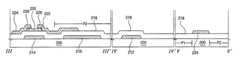
도 4a 내지 도 4d는 도 3의 Ⅲ-Ⅲ`와 Ⅳ-Ⅳ `와 Ⅴ-Ⅴ`를 따라 절단하여, 본 발명의 공정 순서에 따라 도시한 공정 단면도이다.
4A through 4D are cross-sectional views taken along the lines III-III ′, IV-IV ′, and V-V ′ of FIG. 3, and according to the process sequence of the present invention.
<도면의 주요 부분에 대한 부호의 설명><Explanation of symbols for the main parts of the drawings>
200 : 투명 절연기판 212 : 게이트 배선200: transparent insulating substrate 212: gate wiring
214 : 게이트 전극 216 : 스토리지 배선214: gate electrode 216: storage wiring
220 : 액티브층 224 : 데이터 배선220: active layer 224: data wiring
226 : 소스 전극 228 : 드레인 전극226: source electrode 228: drain electrode
238 : 화소 전극 240 : 공통 전극
238: pixel electrode 240: common electrode
본 발명은 액정 표시장치에 관한 것으로 특히, 미세 화소를 구현하기 위한 횡전계방식(In-Plane Switching mode) 액정표시장치용 어레이기판과 그 제조방법에 관한 것이다.BACKGROUND OF THE
일반적으로 액정표시장치의 구동원리는 액정의 광학적 이방성과 분극성질을 이용한다.In general, the driving principle of the liquid crystal display device uses the optical anisotropy and polarization of the liquid crystal.
상기 액정은 구조가 가늘고 길기 때문에 분자의 배열에 방향성을 가지고 있으며, 인위적으로 액정에 전기장을 인가하여 분자배열의 방향을 제어할 수 있다.Since the liquid crystal is thin and long in structure, the liquid crystal has directivity in the arrangement of molecules, and the direction of the molecular arrangement can be controlled by artificially applying an electric field to the liquid crystal.
따라서, 상기 액정의 분자배열 방향을 임의로 조절하면, 액정의 분자배열이 변하게 되고, 광학적 이방성에 의하여 편광된 빛이 임의로 변조되어 화상정보를 표현할 수 있다.Accordingly, when the molecular arrangement direction of the liquid crystal is arbitrarily adjusted, the molecular arrangement of the liquid crystal is changed, and light polarized by optical anisotropy may be arbitrarily modulated to express image information.
현재에는 박막 트랜지스터와 상기 박막 트랜지스터에 연결된 화소전극이 행렬 방식으로 배열된 능동행렬 액정표시장치(Active Matrix LCD : AM-LCD)가 해상도 및 동영상 구현능력이 우수하여 가장 주목받고 있다.Currently, active matrix LCDs (AM-LCDs) in which thin film transistors and pixel electrodes connected to the thin film transistors are arranged in a matrix manner have attracted the most attention due to their excellent resolution and video performance.
이하, 도면을 참조하여 종래의 횡전계 방식 액정표시장치용 어레이기판과 그 제조방법에 대해 설명한다.Hereinafter, a conventional array substrate for a transverse electric field type liquid crystal display device and a manufacturing method thereof will be described with reference to the drawings.
도 1은 종래의 횡전계 방식 액정표시장치용 어레이기판의 한 화소를 개략적으로 도시한 평면도이다.1 is a plan view schematically showing one pixel of a conventional array substrate for a transverse electric field type liquid crystal display device.
도시한 바와 같이, 종래의 횡전계방식 액정표시장치용 어레이기판(10)은 소정간격 이격되어 평행하게 일 방향으로 구성된 다수의 게이트배선(12)과, 상기 게이트 배선(12)에 근접하여 평행하게 일 방향으로 구성된 스토리지 배선(16)과, 상기 두 배선과 교차하며 특히 게이트배선(12)과는 화소영역(P)을 정의하는 데이터배선(24)이 구성된다.As shown in the drawing, a
상기 게이트배선(12)과 데이터배선(24)의 교차지점에는 게이트 전극(14)과 액티브층(20)과 소스 전극(26)및 드레인 전극(28)을 포함하는 박막트랜지스터(T)가 구성되며, 상기 소스 전극(26)은 상기 데이터 배선(24)과 연결되고, 상기 게이트 전극(14)은 상기 게이트배선(12)과 연결된다.The thin film transistor T including the
상기 화소영역(P)의 상부에는 상기 드레인 전극(28)과 연결되는 화소 전극(30)과, 상기 화소 전극(30)과 평행하게 구성되고 상기 스토리지 배선(16)과 연결되는 공통전극(17)이 구성된다.The
상기 화소전극(30)은 상기 드레인 전극(28)에서 연장된 연장부(30a)와 상기 연장부(30a)에서 수직하게 연장되고 서로 소정간격 이격된 다수의 수직부(30b)와, 상기 스토리지배선(16)의 상부에서 수직부(30b)를 하나로 연결하는 수평부(30c)로 구성된다.The
상기 공통전극(17)은 상기 스토리지배선(16)에서 아래로 수직하게 연장되고, 상기 화소전극의 수직부(30b)와 엇갈려 구성되는 다수의 수직부(17b)와, 상기 각 수직부(17b)를 하나로 연결하는 수평부(17a)로 구성된다.The
전술한 바와 같은 구성은 상기 게이트 배선(12)과 근접하게 공통전극(17)과 화소전극(30)이 구성되어 있다.As described above, the
상기 게이트 배선(12)과 화소 및 공통전극(30, 17)의 사이영역(D)은 상기 공통전극(17)과 화소전극(30) 사이에 발생하는 전계와는 다른 분포를 가지는 전계가 형성되기 때문에 액정의 이상 배향이 발생하는 영역이다.The region D between the
따라서, 이 영역은 표시영역으로 사용할 수 없다.
Therefore, this area cannot be used as the display area.
따라서, 본 발명은 미소화소의 개구율과 휘도를 개선하기 위한 목적으로 안출된 것으로, 전술한 비표시 영역에 스토리지 배선을 설계하고, 상기 스토리지 배선 상부에 보조 용량부를 구성하는 동시에 상기 각 화소영역 마다 구성되는 투명한 공통전극이 콘택홀을 통해 스토리지 배선과 연결되도록 하는 구조를 제안한다.
Accordingly, the present invention is conceived for the purpose of improving the aperture ratio and luminance of a micropixel, and designing a storage wiring in the non-display area described above, and forming a storage capacitor on the storage wiring, and configuring the respective pixel areas. The present invention proposes a structure in which a transparent common electrode is connected to a storage line through a contact hole.
전술한 목적을 달성하기 위한 본 발명에 따른 횡전계 방식 액정표시장치용 어레이기판은, 다수의 화소영역이 정의된 투명 절연기판과; 상기 화소영역의 일 측에 일 방향으로 구성된 다수의 게이트 배선과 스토리지 배선과; 상기 게이트 배선 및 스토리지 배선과 제 1 절연막을 사이에 두고 교차하는 데이터 배선과; 상기 게이트 배선과 데이터배선의 교차지점에 위치하고, 게이트 전극과 액티브층과 소스 전극 및 드레인 전극을 포함하는 박막트랜지스터와; 상기 게이트 배선과 데이터 배선과 스토리지 배선과 박막트랜지스터의 상부에 구성된 제 2 절연막과; 상기 드레인 전극의 일부를 노출하도록 제 2 절연막을 식각한 제 1 콘택홀과, 상기 스토리지 배선의 일부를 노출하도록 제 1 절연막과 제 2 절연막을 식각한 제 2 콘택홀과; 상기 제 1 콘택홀을 통해 드레인 전극과 접촉하면서 상기 화소영역 내에 구성된 화소전극과; 상기 제 2 콘택홀을 통해 스토리지 배선과 접촉하면서 상기 화소전극과 이격되어 구성된 공통전극을 포함하며, 상기 스토리지 배선의 일부를 제 1 전극으로 하고 상기 드레인 전극의 일부를 제 2 전극으로 하는 제 1 보조 용량부와, 상기 게이트 배선의 일부를 제 1 전극으로 하고 상기 화소전극의 일부를 제 2 전극으로 하는 제 2 보조 용량부가 구성된다.An array substrate for a transverse electric field type liquid crystal display device according to the present invention for achieving the above object includes a transparent insulating substrate having a plurality of pixel areas defined; A plurality of gate lines and storage lines formed in one direction on one side of the pixel area; A data line crossing the gate line and the storage line and having a first insulating layer therebetween; A thin film transistor positioned at an intersection point of the gate line and the data line, the thin film transistor including a gate electrode, an active layer, a source electrode, and a drain electrode; A second insulating film formed over the gate wiring, the data wiring, the storage wiring, and the thin film transistor; A first contact hole etched from the second insulating film to expose a portion of the drain electrode, and a second contact hole etched from the first insulating film and the second insulating film to expose a portion of the storage wiring; A pixel electrode formed in the pixel region while in contact with the drain electrode through the first contact hole; A first auxiliary electrode including a common electrode configured to be spaced apart from the pixel electrode while being in contact with the storage wiring through the second contact hole, wherein a part of the storage wiring is a first electrode and a part of the drain electrode is a second electrode; A capacitor portion and a second auxiliary capacitor portion including a portion of the gate wiring as a first electrode and a portion of the pixel electrode as a second electrode are provided.
삭제delete
상기 공통전극과 화소전극은 인듐-틴-옥사이드(ITO)와 인듐-징크-옥사이드(IZO)를 포함한 투명 도전성 금속그룹 중 선택된 하나로 형성한다.The common electrode and the pixel electrode are formed of one selected from a group of transparent conductive metals including indium tin oxide (ITO) and indium zinc oxide (IZO).
상기 공통전극은 하나의 동일한 화소영역 내에서는 상기 화소전극을 사이에 두고 이격하여 형성되며, 서로 이웃한 화소영역 간의 경계에 위치한 상기 데이터 배선과 교차하는 수평부가 더욱 구성되어 상기 서로 이웃한 화소영역 간에 인접한 공통전극은 상기 수평부를 통해 서로 연결된 것이 특징이다.The common electrode is formed to be spaced apart from each other within the same pixel region, and a horizontal portion intersecting the data line positioned at a boundary between neighboring pixel regions is further configured to intersect the neighboring pixel regions. Adjacent common electrodes are connected to each other through the horizontal part.
본 발명의 특징에 따른 횡전계 방식 액정표시장치용 어레이기판 제조방법은, 투명 절연 기판 상에 다수의 화소영역을 정의하는 단계와; 상기 화소영역의 일 측에 일 방향으로 구성된 다수의 게이트 배선과, 스토리지 배선을 형성하는 단계와; 상기 게이트 배선 및 스토리지 배선과 제 1 절연막을 사이에 두고 교차하는 데이터 배선을 형성하는 단계와; 상기 게이트 배선과 데이터배선의 교차지점에 위치하고, 게이트 전극과 액티브층과 소스 전극 및 드레인 전극을 포함하는 박막트랜지스터를 형성하는 단계와; 상기 게이트배선과 데이터 배선과 스토리지 배선과 박막트랜지스터의 상부에 제 2 절연막을 형성하고, 상기 드레인 전극 일부를 노출하는 제 1 콘택홀과, 상기 스토리지 배선의 일부를 노출하는 제 2 콘택홀을 형성하는 단계와; 상기 제 1 콘택홀을 통해 상기 드레인 전극과 접촉하면서 상기 화소영역 내에 화소전극을 형성하며, 동시에 상기 스토리지 배선의 일부를 제 1 전극으로 하고 상기 드레인 전극의 일부를 제 2 전극으로 하는 제 1 보조 용량부와, 상기 게이트 배선의 일부를 제 1 전극으로 하고 상기 화소전극의 일부를 제 2 전극으로 하는 제 2 보조 용량부를 형성하는 단계와; 상기 제 2 콘택홀을 통해 상기 스토리지배선과 접촉하면서 상기 화소전극과 이격된 공통전극을 형성하는 단계를 포함한다.According to an aspect of the present invention, there is provided a method of fabricating an array substrate for a transverse electric field type liquid crystal display device, comprising: defining a plurality of pixel regions on a transparent insulating substrate; Forming a plurality of gate lines and storage lines formed in one direction on one side of the pixel area; Forming a data line intersecting the gate line and the storage line with a first insulating layer interposed therebetween; Forming a thin film transistor positioned at an intersection point of the gate line and the data line, the thin film transistor including a gate electrode, an active layer, a source electrode, and a drain electrode; Forming a second insulating layer on the gate wiring, the data wiring, the storage wiring, and the thin film transistor, forming a first contact hole exposing a portion of the drain electrode, and a second contact hole exposing a portion of the storage wiring; Steps; A first storage capacitor is formed in the pixel region while contacting the drain electrode through the first contact hole, and at the same time, a part of the storage wiring as a first electrode and a part of the drain electrode as a second electrode. And a second storage capacitor portion including a portion of the gate wiring as a first electrode and a portion of the pixel electrode as a second electrode; And forming a common electrode spaced apart from the pixel electrode while contacting the storage wiring through the second contact hole.
상기 공통전극과 화소전극은 인듐-틴-옥사이드(ITO)와 인듐-징크-옥사이드(IZO)를 포함한 투명 도전성 금속그룹 중 선택된 하나로 형성하며, 상기 공통전극은 하나의 동일한 화소영역 내에서는 상기 화소전극을 사이에 두고 이격하여 형성되며, 서로 이웃한 화소영역 간의 경계에 위치한 상기 데이터 배선과 교차하는 수평부가 더욱 구성되어 상기 수평부에 의해 상기 서로 이웃한 화소영역 간에 인접한 공통전극은 서로 연결되도록 형성되는 것이 특징이다.The common electrode and the pixel electrode are formed of one selected from a group of transparent conductive metals including indium tin oxide (ITO) and indium zinc oxide (IZO), and the common electrode is the pixel electrode in one same pixel area. A horizontal portion intersecting the data line positioned at a boundary between neighboring pixel regions is further formed so that the common electrodes adjacent to each other adjacent pixel regions are connected to each other by the horizontal portion. Is characteristic.
이하, 첨부된 도면을 참조하여 본 발명에 따른 바람직한 실시예를 설명한다.Hereinafter, exemplary embodiments of the present invention will be described with reference to the accompanying drawings.
-- 제 1 실시예 --First Embodiment
도 2는 본 발명의 제 1 실시예에 따른 횡전계 방식 액정표시장치용 어레이기판의 일부를 개략적으로 도시한 평면도이다.2 is a plan view schematically illustrating a part of an array substrate for a transverse electric field type liquid crystal display device according to a first embodiment of the present invention.
도시한 바와 같이, 본 발명의 횡전계 방식 액정표시장치용 어레이기판(100)은 소정간격 이격되어 평행하게 일 방향으로 구성된 다수의 게이트배선(112)과 스토리지 배선(116)과, 상기 두 배선과 교차하며 특히 게이트배선(112)과는 화소영역(P)을 정의하는 데이터배선(124)이 구성된다.As illustrated, the
상기 게이트배선(112)과 데이터배선(124)의 교차지점에는, 상기 게이트 배선(112)과 연결된 게이트 전극(114)과, 상기 게이트 전극(114)의 상부에 구성된 액티브층(120)과 소스 전극(126)및 드레인 전극(128)을 포함하는 박막트랜지스터(T)가 구성되며, 상기 소스 전극(126)은 상기 데이터배선(124)과 연결되고, 상기 게이트 전극(114)은 상기 게이트배선(112)과 연결된다.At the intersection of the
상기 화소영역(P)에는 상기 드레인 전극(128)과 연결되는 화소전극(130)과, 상기 화소전극(130)과 평행하게 구성되고 상기 스토리지 배선(116)과 연결되는 공통전극(117)이 구성된다.The pixel region P includes a
상기 화소전극(130)은 스토리지 배선(116)의 상부에서 상기 드레인 전극(128)과 연결되면서 화소영역(P)으로 수직한 형상으로 구성된다.The
상기 공통전극(117)은 상기 게이트 배선(112)과 소정간격 평행하게 이격되어 화소영역(P)에 형성된 수평부(117a)와, 상기 수평부(117a)의 양측에서 화소영역(P)으로 상기 화소전극(130)을 사이에 두고 수직하게 연장된 수직부(117b)로 구성된다.The
상기 공통전극의 수평부(117a)는 이웃한 화소영역으로 연장 형성된다.The
상기 공통전극(117)과 화소전극(130)은 개구율을 높이기 위해 별도의 투명전극으로 형성한다.The
상기 공통전극(117)은 하부의 스토리지 배선(116)에서 공통신호를 인가 받아야 하기 때문에, 제 1 콘택홀(137)을 통해 스토리지배선(116)과 접촉하도록 구성하고, 상기 화소전극(130)은 드레인 전극(128)을 통해 신호를 인가 받아야 하기 때문에 제 2 콘택홀(139)을 통해 드레인 전극(128)과 접촉하도록 구성된다.Since the
상기 스토리지 배선(116)의 상부에는 보조 용량부(C)가 구성되며, 스토리지 배선(116)의 일부를 제 1 전극으로 이와는 평면적으로 겹쳐지는 드레인 전극(128) 의 일부를 제 2 전극으로 한다.A storage capacitor portion C is formed above the
전술한 바와 같은 구성으로 종래에 따른 횡전계 방식 액정표시장치용 어레이기판을 구성할 수 있다.With the configuration as described above, a conventional array substrate for a transverse electric field type liquid crystal display device can be constructed.
이하, 제 2 실시예는 상기 제 1 실시예를 변형한 것으로, 게이트 배선의 상부에 별도의 보조 용량부를 더욱 구성하고, 상기 화소영역에 구성되는 공통전극의 면적을 줄여 개구율을 개선하고자 한다.Hereinafter, the second embodiment is modified from the first embodiment, and an additional storage capacitor is further formed on the upper portion of the gate wiring, and the area ratio of the common electrode formed in the pixel area is reduced to improve the aperture ratio.
-- 제 2 실시예 --Second Embodiment
본 발명은 스토리지 배선과 게이트 배선의 상부에 제 1 보조 용량부와 제 2 보조 용량부를 구성하고, 화소영역을 차지하는 공통전극의 면적을 줄이기 위한 공통전극 구조를 새롭게 설계하는 것을 특징으로 한다.The present invention is characterized in that the first storage capacitor and the second storage capacitor are formed on the storage wiring and the gate wiring, and the common electrode structure is newly designed to reduce the area of the common electrode occupying the pixel area.
도 3은 본 발명의 제 2 실시예에 따른 횡전계 방식 액정표시장치용 어레이기판의 일부를 개략적으로 도시한 평면도이다.3 is a plan view schematically illustrating a part of an array substrate for a transverse electric field type liquid crystal display device according to a second exemplary embodiment of the present invention.
도시한 바와 같이, 본 발명에 따른 횡전계방식 액정표시장치용 어레이기판(200)은 소정간격 이격되어 평행하게 일 방향으로 구성된 다수의 게이트배선(212)과 스토리지 배선(216)과, 상기 두 배선과 교차하며 게이트배선(212)과는 화소영역(P1,P2)을 정의하는 데이터배선(224)을 구성한다.As illustrated, the
상기 게이트배선(212)과 데이터배선(224)의 교차지점에는 게이트 전극(214)과 액티브층(220)과 소스 전극(226) 및 드레인 전극(228)을 포함하는 박막트랜지스터(T)를 구성하며, 상기 소스 전극(226)은 상기 데이터배선(224)과 연결하고, 상기 게이트 전극(214)은 상기 게이트배선(212)과 연결한다.A thin film transistor T including a
상기 드레인 전극(228)은 상기 스토리지 배선(216)의 상부로 연장 형성한다.The
상기 화소영역(P1,P2)의 상부에는 상기 드레인 전극(228)과 연결되는 화소전극(238)과, 상기 화소전극(238)과 평행하게 구성되고 상기 스토리지 배선(216)과 연결되는 공통전극(240)을 구성한다.The pixel electrode 238 connected to the
상기 화소전극(238)은 상기 스토리지 배선(216)의 상부로 연장된 드레인 전극(228)의 일부와 접촉하면서 화소영역(P2)으로 수직하게 연장된 수직부(238a)와, 상기 수직부(238a)에서 게이트 배선(212)을 따라 연장된 수평부(238b)로 구성한다.The pixel electrode 238 vertically extends into the pixel region P2 while contacting a portion of the
상기 공통전극(240)은 상기 스토리지 배선(216)과 연결되면서 상기 데이터배선과 근접하여 화소영역(P2)으로 수직하게 구성된 수직부(240a)와, 상기 수직부(240a)에서 상기 데이터 배선(224)의 상부로 연장된 수평부(240b)와, 상기 수평부(240b)에서 이웃한 화소영역(P1)으로 수직하게 연장된 제 2 수직부(240c)로 구성한다.The
전술한 본 발명의 어레이기판 구성은 종래의 구성과는 달리 화소영역에 구성되는 공통전극의 수평부(도 2의 117a)를 생략한 구조이므로 그만큼의 개구율을 확보할 수 있다. Unlike the conventional structure, the array substrate of the present invention has a structure in which the horizontal portion (117a of FIG. 2) of the common electrode of the pixel region is omitted, thereby ensuring the same aperture ratio.
또한, 스토리지 배선(216)의 일부를 제 1 전극으로 하고, 상기 스토리지 배선(216)의 상부에 연장된 드레인 전극(228)의 일부를 제 2 전극으로 하는 제 1 보조 용량부(C1)와, 상기 게이트 배선(212)의 일부를 제 1 전극으로 하고 상기 화소전극의 수평부(238b)를 제 2 전극으로 하는 제 2 보조 용량부(C2)가 구성되어, 보조 용량을 충분히 확보할 수 있는 구조이다.In addition, a first storage capacitor C1 having a portion of the
이하, 도 4a 내지 도 4d를 참조하여, 본 발명에 따른 횡전계 방식 액정표시장치용 어레이기판의 제조방법을 설명한다.Hereinafter, a method of manufacturing an array substrate for a transverse electric field type liquid crystal display device according to the present invention will be described with reference to FIGS. 4A to 4D.
도 4a 내지 도 4d는 도 3의 Ⅲ-Ⅲ`와 Ⅳ-Ⅳ`와 Ⅴ-Ⅴ`를 따라 절단하여, 본 발명의 공정순서에 따라 도시한 공정 단면도이다.4A through 4D are cross-sectional views taken along the line III-III ′, IV-IV ′, and V-V ′ of FIG. 3, according to a process sequence of the present invention.
도 4a에 도시한 바와 같이, 기판(200)상에 알루미늄(Al), 알루미늄 네오디뮴(AlNd)과 같은 알루미늄 합금, 크롬(Cr), 몰리브덴(Mo), 텅스텐(W)을 포함하는 도전성 금속그룹 중 선택된 하나를 증착하여, 게이트 전극(214)을 포함하는 게이트배선(212)과, 상기 게이트배선(212)과 소정간격 평행하게 이격된 스토리지배선(216)을 형성한다.As shown in FIG. 4A, a conductive metal group including an aluminum alloy such as aluminum (Al), aluminum neodymium (AlNd), chromium (Cr), molybdenum (Mo), and tungsten (W) on the
다음으로, 상기 게이트배선(212)과 스토리지배선(216) 등이 포함된 기판(200)의 전면에 질화 실리콘(SiNX)과 산화 실리콘(SiO2)을 포함하는 무기절연물질 그룹 중 선택된 하나를 증착하여 게이트 절연막(218)을 형성한다.Next, one selected from the group of inorganic insulating materials including silicon nitride (SiNX ) and silicon oxide (SiO2 ) on the front surface of the
다음으로, 상기 게이트 절연막(218) 상부에 비정질 실리콘(a-Si:H)과 불순물이 포함된 비정질 실리콘(n+a-Si:H)을 증착하고 패턴하여, 액티브층(220)과 오믹 콘택층(222)을 형성한다.Next, amorphous silicon (a-Si: H) and amorphous silicon (n + a-Si: H) containing impurities are deposited on the
도 4b에 도시한 바와 같이, 상기 액티브층(220)과 오믹 콘택층(222)이 형성된 기판(200)의 전면에 전술한 바와 같은 도전성 금속그룹 중 선택된 하나를 증착하고 패턴하여, 상기 게이트배선(212)과 스토리지배선(216)과 교차하여 화소영역(P1,P2)을 정의하는 데이터배선(224)과, 상기 데이터배선(224)에서 돌출 형성되고 상기 액티브층(220)의 일측 상부에 겹쳐 구성되는 소스 전극(226)과 이와는 소정간격 이격된 드레인 전극(228)을 형성한다.As shown in FIG. 4B, one of the conductive metal groups as described above is deposited and patterned on the entire surface of the
전술한 공정에서, 상기 소스 전극(226)과 드레인 전극(228)을 마스크로 하여 상기 두 전극 사이에 노출된 오믹 콘택층(222)을 식각하여 액티브층(220)을 노출한다.In the above-described process, the
도 4c에 도시한 바와 같이, 상기 소스 및 드레인 전극(226,228)과 데이터 배선(224)이 형성된 기판(200)의 전면에 질화 실리콘(SiNx)과 산화 실리콘(SiO2)을 포함한 무기절연 물질 그룹 중 선택된 하나 또는 벤조사이클로부텐(BCB)과 아크릴(Acryl)계 수지를 포함한 유기절연물질 그룹 중 선택된 하나를 증착 또는 도포하여 보호막(232)을 형성한다.As shown in FIG. 4C, an inorganic insulating material group including silicon nitride (SiNx ) and silicon oxide (SiO2 ) on the entire surface of the
연속하여, 상기 보호막(232)을 패턴하여, 상기 스토리지 배선(216)의 상부로 연장된 드레인 전극(228)의 일부를 노출하는 제 1 콘택홀(234)과, 상기 스토리지 배선(216)의 일부를 노출하는 제 2 콘택홀(236)을 형성한다.Subsequently, the
도 4d에 도시한 바와 같이, 상기 보호막(232)이 형성된 기판(200)의 전면에 인듐-틴-옥사이드(ITO)와 인듐-징크-옥사이드(IZO)를 포함한 투명 도전성 금속 물질 그룹 중 선택된 하나를 증착하고 패턴하여, 상기 제 1 콘택홀(234)과 접촉하면서 상기 화소영역(P2)으로 연장된 수직부(238a)와, 상기 수직부(238a)에서 연장되고 상기 게이트 배선(212)의 상부에서 일 방향으로 연장된 수평부(238b)를 형성한다.As shown in FIG. 4D, one selected from the group of transparent conductive metal materials including indium tin oxide (ITO) and indium zinc oxide (IZO) on the front surface of the
동시에, 상기 화소전극(238)과 소정간격 평행하게 이격되고, 상기 제 2 콘택홀(236)을 통해 스토리지 배선(216)과 연결되며, 상기 데이터 배선(224)에 근접하게 화소영역(P)으로 연장된 제 1 수직부(240a)와, 상기 게이트 배선(212)과 근접한 영역에서 상기 제 1 수직부(240a)에서 데이터 배선(224)의 상부로 수평하게 연장된 수평부(240b)와, 상기 수평부(240b)에서 이웃한 화소영역(P1)으로 수직하게 연장된 제 2 수직부(240c)로 구성된 공통전극을 형성한다.At the same time, the pixel electrode 238 is spaced apart in parallel with a predetermined interval, and is connected to the
전술한 바와 같은 공정을 통해 본 발명에 따른 액정표시장치용 어레이기판을 제작할 수 있다.Through the process as described above it can be produced an array substrate for a liquid crystal display device according to the present invention.
본 발명은 게이트 배선의 상부에 제 1 보조용량부가 구성되고, 상기 스토리지 배선의 상부에 제 2 보조용량부가 구성되어 보조 용량을 충분히 확보할 수 있는 것을 제 1 특징으로 한다.The present invention is characterized in that the first storage capacitor portion is formed on the upper portion of the gate wiring, and the second storage capacitor portion is formed on the storage wiring.
또한, 제 1 실시예와 비교하여 화소영역을 차지하는 공통전극의 전체 면적이 작아지는 구조이므로 개구율을 확보할 수 있는 것을 제 2 특징으로 한다.
In addition, the second aspect of the present invention is that the aperture ratio can be ensured because the total area of the common electrode occupying the pixel region is smaller than that of the first embodiment.
따라서, 본 발명에 따른 횡전계 방식 액정표시장치용 어레이기판은 화소의 면적이 작아지더라도 충분한 스토리지 용량확보가 가능하고 개구율이 개선되는 구조이므로 미세 화소에 적용가능하여, 고 화질, 고 해상도를 가지는 대면적 액정패널을 제작할 수 있는 효과가 있다.
Therefore, the array substrate for a transverse electric field type liquid crystal display device according to the present invention is capable of securing sufficient storage capacity even when the area of the pixel is small, and thus can be applied to fine pixels because it has an improved aperture ratio. There is an effect that can produce a large area liquid crystal panel.
Claims (6)
Translated fromKoreanPriority Applications (2)
| Application Number | Priority Date | Filing Date | Title |
|---|---|---|---|
| KR1020010088750AKR100801153B1 (en) | 2001-12-31 | 2001-12-31 | Array board for transverse electric field type liquid crystal display device and manufacturing method thereof |
| US10/330,124US6924864B2 (en) | 2001-12-31 | 2002-12-30 | Array substrate for in-plane switching mode liquid crystal display device and method of fabricating the same |
Applications Claiming Priority (1)
| Application Number | Priority Date | Filing Date | Title |
|---|---|---|---|
| KR1020010088750AKR100801153B1 (en) | 2001-12-31 | 2001-12-31 | Array board for transverse electric field type liquid crystal display device and manufacturing method thereof |
Publications (2)
| Publication Number | Publication Date |
|---|---|
| KR20030058334A KR20030058334A (en) | 2003-07-07 |
| KR100801153B1true KR100801153B1 (en) | 2008-02-05 |
Family
ID=19717986
Family Applications (1)
| Application Number | Title | Priority Date | Filing Date |
|---|---|---|---|
| KR1020010088750AExpired - LifetimeKR100801153B1 (en) | 2001-12-31 | 2001-12-31 | Array board for transverse electric field type liquid crystal display device and manufacturing method thereof |
Country Status (2)
| Country | Link |
|---|---|
| US (1) | US6924864B2 (en) |
| KR (1) | KR100801153B1 (en) |
Families Citing this family (20)
| Publication number | Priority date | Publication date | Assignee | Title |
|---|---|---|---|---|
| KR100560401B1 (en) | 2003-11-04 | 2006-03-14 | 엘지.필립스 엘시디 주식회사 | Horizontal field applied thin film transistor substrate and manufacturing method thereof |
| JP4424925B2 (en)* | 2003-06-05 | 2010-03-03 | 株式会社 日立ディスプレイズ | Display device |
| KR100556702B1 (en)* | 2003-10-14 | 2006-03-07 | 엘지.필립스 엘시디 주식회사 | Thin film transistor substrate for display element and manufacturing method thereof |
| KR100560400B1 (en)* | 2003-11-04 | 2006-03-14 | 엘지.필립스 엘시디 주식회사 | Horizontal field applied thin film transistor substrate and manufacturing method thereof |
| KR100560402B1 (en)* | 2003-11-04 | 2006-03-14 | 엘지.필립스 엘시디 주식회사 | Horizontal field applied thin film transistor substrate and manufacturing method thereof |
| KR100560403B1 (en)* | 2003-11-04 | 2006-03-14 | 엘지.필립스 엘시디 주식회사 | Horizontal field applied thin film transistor substrate and manufacturing method thereof |
| KR101039022B1 (en)* | 2004-02-11 | 2011-06-03 | 삼성전자주식회사 | Contact portion and manufacturing method thereof, thin film transistor array panel and manufacturing method thereof |
| KR101157386B1 (en)* | 2005-02-02 | 2012-06-20 | 엘지디스플레이 주식회사 | Liquid crystal display device and method for manufacturing lcd |
| TW200706955A (en)* | 2005-08-08 | 2007-02-16 | Innolux Display Corp | In-plane switching liquid crystal display device |
| TW200730978A (en)* | 2006-02-08 | 2007-08-16 | Wintek Corp | Active matrix liquid crystal display and pixel structure thereof |
| KR20070109521A (en)* | 2006-05-11 | 2007-11-15 | 삼성전자주식회사 | A thin film transistor substrate, a liquid crystal display panel including the same, and a manufacturing method of the liquid crystal display panel |
| US8106865B2 (en) | 2006-06-02 | 2012-01-31 | Semiconductor Energy Laboratory Co., Ltd. | Display device and driving method thereof |
| KR101350669B1 (en)* | 2007-01-31 | 2014-01-10 | 엘지디스플레이 주식회사 | Liquid crystal display device and method of fabricating the same |
| KR101329284B1 (en)* | 2007-02-08 | 2013-11-14 | 삼성디스플레이 주식회사 | Display substrate and method for manufacturing the same |
| TWI435153B (en) | 2010-12-28 | 2014-04-21 | Au Optronics Corp | Pixel structure |
| TWI412858B (en) | 2010-12-29 | 2013-10-21 | Au Optronics Corp | Pixel structure |
| TWI492389B (en)* | 2012-07-13 | 2015-07-11 | Au Optronics Corp | Pixel structure and pixel structure manufacturing method |
| CN104813386B (en)* | 2012-11-30 | 2017-05-31 | 夏普株式会社 | TFT substrate |
| CN103325794A (en)* | 2013-05-30 | 2013-09-25 | 合肥京东方光电科技有限公司 | Array substrate, display device and method for manufacturing array substrate |
| CN109061971A (en)* | 2018-09-07 | 2018-12-21 | 京东方科技集团股份有限公司 | Array substrate and display panel |
Citations (7)
| Publication number | Priority date | Publication date | Assignee | Title |
|---|---|---|---|---|
| KR960008377A (en)* | 1994-08-24 | 1996-03-22 | 가나이 쯔도무 | Active Matrix Liquid Crystal Display |
| KR960036533A (en)* | 1995-03-03 | 1996-10-28 | 기따오까 다까시 | Display device |
| JPH08327978A (en)* | 1995-05-30 | 1996-12-13 | Hitachi Ltd | Active matrix liquid crystal display device |
| KR19990009891A (en)* | 1997-07-12 | 1999-02-05 | 구자홍 | Transverse electric field liquid crystal display device |
| JPH11271807A (en)* | 1998-03-25 | 1999-10-08 | Hitachi Ltd | Active matrix substrate and liquid crystal display |
| JP2001330846A (en)* | 2001-04-02 | 2001-11-30 | Advanced Display Inc | Liquid crystal display device |
| KR20010106862A (en)* | 2000-05-23 | 2001-12-07 | 구본준, 론 위라하디락사 | IPS mode Liquid crystal display device and method for fabricating the same |
Family Cites Families (13)
| Publication number | Priority date | Publication date | Assignee | Title |
|---|---|---|---|---|
| EP0588568B1 (en) | 1992-09-18 | 2002-12-18 | Hitachi, Ltd. | A liquid crystal display device |
| JPH095764A (en) | 1995-06-20 | 1997-01-10 | Hitachi Ltd | LCD display substrate |
| JP3474975B2 (en) | 1995-09-06 | 2003-12-08 | 株式会社 日立ディスプレイズ | Liquid crystal display device and method of manufacturing the same |
| JPH09105908A (en) | 1995-10-09 | 1997-04-22 | Hitachi Ltd | Active matrix type liquid crystal display |
| JP3632934B2 (en) | 1995-10-04 | 2005-03-30 | 株式会社 日立ディスプレイズ | Active matrix liquid crystal display device |
| US5745207A (en) | 1995-11-30 | 1998-04-28 | Matsushita Electric Industrial Co., Ltd. | Active matrix liquid crystal display having electric fields parallel to substrates |
| JP3396130B2 (en) | 1996-06-03 | 2003-04-14 | シャープ株式会社 | Liquid crystal display |
| JP2776376B2 (en) | 1996-06-21 | 1998-07-16 | 日本電気株式会社 | Active matrix liquid crystal display panel |
| US6005648A (en) | 1996-06-25 | 1999-12-21 | Semiconductor Energy Laboratory Co., Ltd. | Display device |
| JPH10142633A (en) | 1996-11-15 | 1998-05-29 | Mitsubishi Electric Corp | Thin film transistor integrated device, method of manufacturing the same, and liquid crystal display device |
| WO1998047044A1 (en)* | 1997-04-11 | 1998-10-22 | Hitachi, Ltd. | Liquid crystal display device |
| JP4130490B2 (en)* | 1997-10-16 | 2008-08-06 | 三菱電機株式会社 | Liquid crystal display |
| JP3228202B2 (en) | 1997-11-18 | 2001-11-12 | 日本電気株式会社 | Lateral electric field type active matrix liquid crystal display device and method of manufacturing the same |
- 2001
- 2001-12-31KRKR1020010088750Apatent/KR100801153B1/ennot_activeExpired - Lifetime
- 2002
- 2002-12-30USUS10/330,124patent/US6924864B2/ennot_activeExpired - Fee Related
Patent Citations (7)
| Publication number | Priority date | Publication date | Assignee | Title |
|---|---|---|---|---|
| KR960008377A (en)* | 1994-08-24 | 1996-03-22 | 가나이 쯔도무 | Active Matrix Liquid Crystal Display |
| KR960036533A (en)* | 1995-03-03 | 1996-10-28 | 기따오까 다까시 | Display device |
| JPH08327978A (en)* | 1995-05-30 | 1996-12-13 | Hitachi Ltd | Active matrix liquid crystal display device |
| KR19990009891A (en)* | 1997-07-12 | 1999-02-05 | 구자홍 | Transverse electric field liquid crystal display device |
| JPH11271807A (en)* | 1998-03-25 | 1999-10-08 | Hitachi Ltd | Active matrix substrate and liquid crystal display |
| KR20010106862A (en)* | 2000-05-23 | 2001-12-07 | 구본준, 론 위라하디락사 | IPS mode Liquid crystal display device and method for fabricating the same |
| JP2001330846A (en)* | 2001-04-02 | 2001-11-30 | Advanced Display Inc | Liquid crystal display device |
Also Published As
| Publication number | Publication date |
|---|---|
| US6924864B2 (en) | 2005-08-02 |
| US20030122990A1 (en) | 2003-07-03 |
| KR20030058334A (en) | 2003-07-07 |
Similar Documents
| Publication | Publication Date | Title |
|---|---|---|
| KR100801153B1 (en) | Array board for transverse electric field type liquid crystal display device and manufacturing method thereof | |
| KR100730495B1 (en) | Transverse electric field type liquid crystal display device and manufacturing method thereof | |
| KR101269002B1 (en) | An array substrate for In-Plane switching mode LCD and method of fabricating of the same | |
| KR100620322B1 (en) | Transverse electric field type liquid crystal display device and manufacturing method thereof | |
| KR100835974B1 (en) | Array board for transverse electric field type liquid crystal display device and manufacturing method thereof | |
| KR100744955B1 (en) | Array board for transverse electric field type liquid crystal display device and manufacturing method thereof | |
| KR100829786B1 (en) | Array board for transverse electric field type liquid crystal display device and manufacturing method thereof | |
| KR101255782B1 (en) | An array substrate for In-Plane switching mode LCD and method of fabricating of the same | |
| KR100835971B1 (en) | Array board for transverse electric field type liquid crystal display device and manufacturing method thereof | |
| KR100835975B1 (en) | Array board for transverse electric field type liquid crystal display device and manufacturing method thereof | |
| KR100844003B1 (en) | Array board for transverse electric field type liquid crystal display device and manufacturing method thereof | |
| KR101609826B1 (en) | Array substrate for fringe field switching mode liquid crystal display device | |
| KR100672215B1 (en) | Transverse electric field type liquid crystal display device and manufacturing method thereof | |
| KR100863727B1 (en) | Array board for transverse electric field type liquid crystal display device and manufacturing method thereof | |
| KR100475837B1 (en) | The substrate for LCD with a repair line and method for fabricating the same | |
| KR101179057B1 (en) | In-Plane Switching Mode Liquid Crystal Display Device and the method of fabricating thereof | |
| KR100835973B1 (en) | Array board for transverse electric field type liquid crystal display device and manufacturing method thereof | |
| KR101086647B1 (en) | Array board for transverse electric field type liquid crystal display device and manufacturing method thereof | |
| KR100918279B1 (en) | Array substrate for liquid crystal display device and manufacturing method | |
| KR100773876B1 (en) | Array board for transverse electric field type liquid crystal display device and manufacturing method thereof | |
| KR101267532B1 (en) | The Liquid Crystal Display Device of a storage on common type and the method for fabricating thereof | |
| KR100816365B1 (en) | Array board for transverse electric field type liquid crystal display device and manufacturing method thereof | |
| KR20060095692A (en) | Array board for transverse electric field type liquid crystal display device and manufacturing method thereof | |
| KR20020037554A (en) | IPS mode Liquid crystal display device and method for fabricating the same | |
| KR100819866B1 (en) | Array board for transverse electric field type liquid crystal display device and manufacturing method thereof |
Legal Events
| Date | Code | Title | Description |
|---|---|---|---|
| PA0109 | Patent application | Patent event code:PA01091R01D Comment text:Patent Application Patent event date:20011231 | |
| PG1501 | Laying open of application | ||
| A201 | Request for examination | ||
| PA0201 | Request for examination | Patent event code:PA02012R01D Patent event date:20061115 Comment text:Request for Examination of Application Patent event code:PA02011R01I Patent event date:20011231 Comment text:Patent Application | |
| E902 | Notification of reason for refusal | ||
| PE0902 | Notice of grounds for rejection | Comment text:Notification of reason for refusal Patent event date:20070920 Patent event code:PE09021S01D | |
| E701 | Decision to grant or registration of patent right | ||
| PE0701 | Decision of registration | Patent event code:PE07011S01D Comment text:Decision to Grant Registration Patent event date:20080128 | |
| GRNT | Written decision to grant | ||
| PR0701 | Registration of establishment | Comment text:Registration of Establishment Patent event date:20080129 Patent event code:PR07011E01D | |
| PR1002 | Payment of registration fee | Payment date:20080130 End annual number:3 Start annual number:1 | |
| PG1601 | Publication of registration | ||
| G170 | Re-publication after modification of scope of protection [patent] | ||
| PG1701 | Publication of correction | ||
| PR1001 | Payment of annual fee | Payment date:20101228 Start annual number:4 End annual number:4 | |
| PR1001 | Payment of annual fee | Payment date:20111221 Start annual number:5 End annual number:5 | |
| FPAY | Annual fee payment | Payment date:20121228 Year of fee payment:6 | |
| PR1001 | Payment of annual fee | Payment date:20121228 Start annual number:6 End annual number:6 | |
| FPAY | Annual fee payment | Payment date:20131227 Year of fee payment:7 | |
| PR1001 | Payment of annual fee | Payment date:20131227 Start annual number:7 End annual number:7 | |
| FPAY | Annual fee payment | Payment date:20141230 Year of fee payment:8 | |
| PR1001 | Payment of annual fee | Payment date:20141230 Start annual number:8 End annual number:8 | |
| FPAY | Annual fee payment | Payment date:20151228 Year of fee payment:9 | |
| PR1001 | Payment of annual fee | Payment date:20151228 Start annual number:9 End annual number:9 | |
| FPAY | Annual fee payment | Payment date:20161214 Year of fee payment:10 | |
| PR1001 | Payment of annual fee | Payment date:20161214 Start annual number:10 End annual number:10 | |
| FPAY | Annual fee payment | Payment date:20171218 Year of fee payment:11 | |
| PR1001 | Payment of annual fee | Payment date:20171218 Start annual number:11 End annual number:11 | |
| FPAY | Annual fee payment | Payment date:20181226 Year of fee payment:12 | |
| PR1001 | Payment of annual fee | Payment date:20181226 Start annual number:12 End annual number:12 | |
| FPAY | Annual fee payment | Payment date:20191212 Year of fee payment:13 | |
| PR1001 | Payment of annual fee | Payment date:20191212 Start annual number:13 End annual number:13 | |
| PR1001 | Payment of annual fee | Payment date:20201222 Start annual number:14 End annual number:14 | |
| PC1801 | Expiration of term | Termination date:20220630 Termination category:Expiration of duration |